Analog Devices AD8303AR, AD8303AN Datasheet
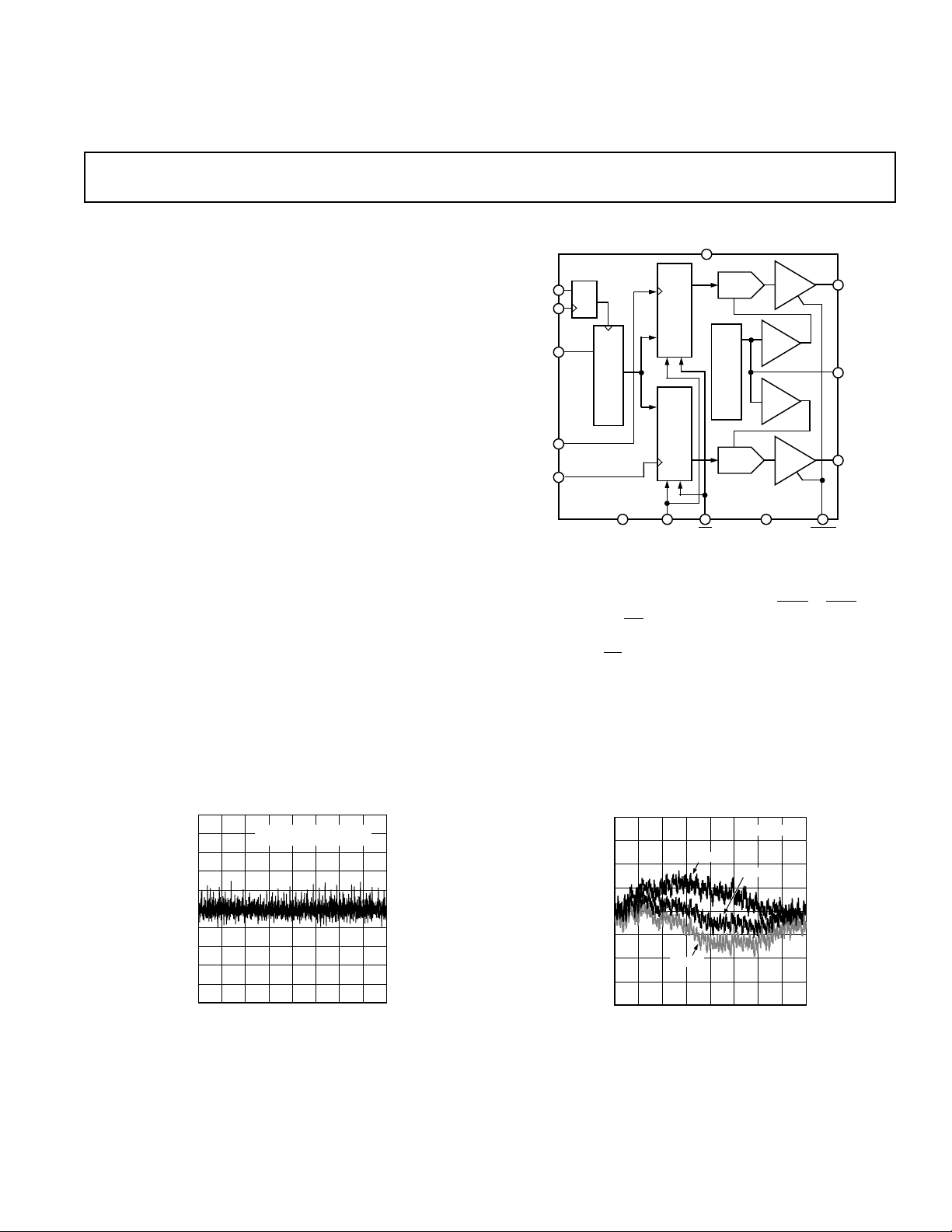
D
A
C
A
R
E
G
I
S
T
E
R
D
PR
En
S
H
I
F
T
R
E
G
I
S
T
E
R
D
A
C
B
R
E
G
I
S
T
E
R
D
PR
R
E
F
E
R
E
N
C
E
B
A
N
D
G
A
P
DAC A
DAC B
V
DD
REF
BUF
REF
BUF
AD8303
V
OUTA
V
REF
V
OUTB
CS
CLK
SDI
(DATA)
LDA
LDB
DGND MSB
RS
AGND
SHDN
OP
AMP
A
OP
AMP
B
+3 V, Dual, Serial Input
a
FEATURES
Complete Dual 12-Bit DAC
Pretrimmed Internal Voltage Reference
Single +3 V Operation
0.5 mV/Bit with 2.0475 V Full Scale
Low Power: 9.6 mW
3-Wire Serial SPI Compatible Interface
Power Shutdown I
Compact SO-14, 1.75 mm Height Package
APPLICATIONS
Portable Communications
Digitally Controlled Calibration
Servo Controls
PC Peripherals
DD
< 1 mA
Complete 12-Bit DAC
AD8303
FUNCTIONAL BLOCK DIAGRAM
GENERAL DESCRIPTION
The AD8303 is a complete (includes internal reference) dual,
12-bit, voltage output digital-to-analog converter designed to
operate from a single +3 volt supply. Built using a CBCMOS
process, this monolithic DAC offers the user low cost and easeof-use in single-supply +3 volt systems. Operation is guaranteed
over the supply voltage range of +2.7 V to +5.5 V making this
device ideal for battery operated applications.
The 2.0475 V full-scale voltage output is laser-trimmed to
maintain accuracy over the operating temperature range of the
device. The binary input data format provides an easy-to-use
one-half millivolt-per-bit software programmability. The voltage
outputs are capable of sourcing 3 mA.
1.0
0.8
0.6
0.4
0.2
0
–0.2
DNL – LSB
–0.4
–0.6
REV. 0
Information furnished by Analog Devices is believed to be accurate and
reliable. However, no responsibility is assumed by Analog Devices for its
use, nor for any infringements of patents or other rights of third parties
which may result from its use. No license is granted by implication or
–0.8
–1.0
Figure 1. Differential Nonlinearity Error vs. Code
0 4096
otherwise under any patent or patent rights of Analog Devices.
VDD = +5V
= –40°C, +25°C, +85°C
T
A
1024 2048 3072
DIGITAL INPUT CODE – Decimal
A double buffered serial data interface offers high speed, threewire, DSP and SPI microcontroller compatible inputs using
data in (SDI), clock (CLK) and load strobe (
pins. A chip-select (
CS) pin simplifies connection of multiple
LDA + LDB)
DAC packages by enabling the clock input when active low.
Additionally, an
RS input sets the output to zero scale or to 1/2
scale based on the level applied to the MSB pin. A power
shutdown feature reduces power dissipation to less than 3 µW.
The AD8303 is specified over the extended industrial (–40°C to
+85°C) temperature range. AD8303s are available in plastic
DIP and low profile 1.75 mm height SO-14 surface mount
packages. For single-channel DAC applications, see the
AD8300 which is offered in the 8-lead DIP and SO-8 packages.
2
1.5
1
0.5
0
–0.5
–1
INL LINEARITY ERROR – LSB
–1.5
–2
0 1024 2048 3072 4096
DIGITAL INPUT CODE – Decimal
–40°C
+85°C
VDD = +5V
+25°C
Figure 2. Linearity Error vs. Digital Code and Temperature
© Analog Devices, Inc., 1996
One Technology Way, P.O. Box 9106, Norwood, MA 02062-9106, U.S.A.
Tel: 617/329-4700 Fax: 617/326-8703

AD8303–SPECIFICATIONS
+3 V OPERATION
(@ VDD = +2.7 V to +3.6 V, –408C ≤ TA ≤ +858C, unless otherwise noted)
Parameter Symbol Condition Min Typ1Max Units
STATIC PERFORMANCE
Resolution
Relative Accuracy
Differential Nonlinearity
Differential Nonlinearity
Zero-Scale Error V
Full-Scale Voltage
Full-Scale Tempco
2
2
2
2
3
3, 4
N 12 Bits
INL –2 ± 1/2 +2 LSB
DNL Monotonic, TA = +25°C –3/4 ±1/4 +3/4 LSB
DNL Monotonic –1 ±1/2 +1 LSB
ZSE
V
FS
TCV
FS
Data = 000
Data = FFF
H
2
H
1.25 +4.5 mV
2.039 2.0475 2.056 Volts
16 ppm/°C
ANALOG OUTPUTS
Output Current I
Output Resistance to GND R
Capacitive Load
4
OUT
C
OUT
L
Data = 800H, ∆V
Data = 000
H
No Oscillation
< 3 mV ±3mA
OUT
3
30 Ω
500 pF
REFERENCE OUTPUT
Output Voltage V
REF
Load > 1 MΩ 1V
LOGIC INPUTS
Logic Input Low Voltage V
Logic Input High Voltage V
Input Leakage Current I
Input Capacitance
4
INTERFACE TIMING SPECIFICATIONS
Clock Width High t
Clock Width Low t
Load Pulse Width t
Data Setup t
Data Hold t
Reset Pulse Width t
Load Setup t
Load Hold t
Select t
Deselect t
AC CHARACTERISTICS
Voltage Output Settling Time
Voltage Output Settling Time
4
6
6
Shutdown Recovery Time t
4, 5
IL
C
CH
CL
LDW
DS
DH
RS
LD1
LD2
CSS
CSH
t
S
t
S
DSR
IL
IH
IL
To ±0.1% of Full Scale 4 µs
To ±1 LSB of Final Value 14 µs
To ±0.1% of Full Scale 10 µs
Output Slew Rate SR Data = 000
to FFFH to 000
H
2.1 V
40 ns
40 ns
40 ns
15 ns
15 ns
40 ns
15 ns
40 ns
40 ns
40 ns
H
0.6 V
10 µA
10 pF
2.0 V/µs
DAC Glitch Q 15 nV/s
Digital Feedthrough Q 15 nV/s
SUPPLY CHARACTERISTICS
Power Supply Range V
Shutdown Current I
Supply Current
7
Power Dissipation P
DD RANGE
DD_SD
I
DD
DISS
DNL < ±1 LSB 2.7 5.5 V
SHDN = 0, No Load, VIL = 0 V, TA = +25°C 0.02 1 µA
V
= 3 V, VIL = 0 V, No Load 2 3.2 mA
DD
V
= 3 V, VIL = 0 V, No Load 6 9.6 mW
DD
Power Supply Sensitivity PSS ∆VDD = ±5% 0.001 0.004 %/%
NOTES
1
Typical readings represent the average value of room temperature operation.
2
1 LSB = 0.5 mV for 0 V to +2.0475 V output range. The first two codes (000H, 001H) are excluded from the linearity error measurement.
3
Includes internal voltage reference error.
4
These parameters are guaranteed by design and not subject to production testing.
5
All input control signals are specified with tR = tF = 2 ns (10% to 90% of +3 V) and timed from a voltage level of 1.6 V.
6
The settling time specification does not apply for negative going transitions within the last 6 LSBs of ground.
7
See Figure 6 for a plot of incremental supply current consumption as a function of the digital input voltage levels.
Specifications subject to change without notice.
REV. 0–2–

SPECIFICATIONS
AD8303
+5 V OPERATION
(@ VDD = +5 V 6 10%, –408C ≤ TA ≤ +858C, unless otherwise noted)
Parameter Symbol Condition Min Typ1Max Units
STATIC PERFORMANCE
Resolution
Relative Accuracy
Differential Nonlinearity
Differential Nonlinearity
Zero-Scale Error V
Full-Scale Voltage
Full-Scale Tempco
2
2
2
2
3
3, 4
N 12 Bits
INL –2 ±1/2 +2 LSB
DNL Monotonic, TA = +25°C –3/4 ±1/4 +3/4 LSB
DNL Monotonic –1 ±1/2 +1 LSB
ZSE
V
FS
TCV
FS
Data = 000
Data = FFF
H
H
1.25 +4.5 mV
2.039 2.0475 2.056 Volts
16 ppm/°C
ANALOG OUTPUTS
Output Current I
Output Resistance to GND R
Capacitive Load
4
OUT
C
OUT
L
Data = 800H, ∆V
Data = 000
H
No Oscillation 500 pF
< 3 mV ±3mA
OUT
30 Ω
REFERENCE OUTPUT
Output Voltage V
REF
Load > 1 MΩ 1V
LOGIC INPUTS
Logic Input Low Voltage V
Logic Input High Voltage V
Input Leakage Current I
Input Capacitance
4
INTERFACE TIMING SPECIFICATIONS
Clock Width High t
Clock Width Low t
Load Pulse Width t
Data Setup t
Data Hold t
Reset Pulse Width t
Load Setup t
Load Hold t
Select t
Deselect t
AC CHARACTERISTICS
Voltage Output Settling Time
Voltage Output Settling Time
4
6
6
Shutdown Recovery Time t
4, 5
IL
C
CH
CL
LDW
DS
DH
RS
LD1
LD2
CSS
CSH
t
S
t
S
SDR
IL
IH
IL
To ±0.1% of Full Scale 4 µs
To ±1 LSB of Final Value
To ±0.1% of Full Scale 10 µs
Output Slew Rate SR Data = 000
to FFFH to 000
H
2.4 V
30 ns
30 ns
30 ns
15 ns
15 ns
30 ns
15 ns
30 ns
30 ns
30 ns
5
H
0.8 V
10 µA
10 pF
12 µs
2V/µs
DAC Glitch Q 15 nV s
Digital Feedthrough Q 15 nV s
SUPPLY CHARACTERISTICS
Power Supply Range V
Shutdown Supply Current I
Positive Supply Current
7
Power Dissipation P
DD RANGE
DD_SD
I
DD
DISS
DNL < ±1 LSB 2.7 3.0 5.5 V
SHDN = 0, No Load, VIL = 0 V, TA = +25°C 0.02 1 µA
V
= 5 V, VIL = 0 V, No Load 2.1 3.4 mA
DD
V
= 5 V, VIL = 0 V, No Load 10.5 17 mW
DD
Power Supply Sensitivity PSS ∆VDD = ±10% 0.001 0.004 %/%
NOTES
1
Typical readings represent the average value of room temperature operation.
2
1 LSB = 0.5 mV for 0 V to +2.0475 V output range. The first two codes (000H, 001H) are excluded from the linearity error measurement.
3
Includes internal voltage reference error.
4
These parameters are guaranteed by design and not subject to production testing.
5
All input control signals are specified with tR = tF = 2 ns (10% to 90% of +5 V) and timed from a voltage level of 1.6 V.
6
The settling time specification does not apply for negative going transitions within the last 6 LSBs of ground.
7
See Figure 6 for a plot of incremental supply current consumption as a function of the digital input voltage levels.
Specifications subject to change without notice.
REV. 0
–3–
AD8303
WARNING!
ESD SENSITIVE DEVICE
ABSOLUTE MAXIMUM RATINGS*
VDD to GND . . . . . . . . . . . . . . . . . . . . . . . . . . . . . –0.3 V, +8 V
Logic Inputs to GND . . . . . . . . . . . . . . . . . . . . . .–0.3 V, +8 V
to GND . . . . . . . . . . . . . . . . . . . . . . –0.3 V, VDD + 0.3 V
V
OUT
Short Circuit to GND . . . . . . . . . . . . . . . . . . . . . . 50 mA
I
OUT
Package Power Dissipation . . . . . . . . . . . . . . . (T
Thermal Resistance θ
JA
J MAX–TA
)/θ
JA
14-Pin Plastic DIP Package (N-14) . . . . . . . . . . . . 103°C/W
14-Lead SOIC Package (R-14) . . . . . . . . . . . . . . . . 158°C/W
Maximum Junction Temperature (T
) . . . . . . . . . . . 150°C
J MAX
Operating Temperature Range . . . . . . . . . . . . –40°C to +85°C
Storage Temperature Range . . . . . . . . . . . . . –65°C to +150°C
Lead Temperature (Soldering, 10 secs) . . . . . . . . . . . . .+300°C
*Stress above those listed under “Absolute Maximum Ratings” may cause perma-
nent damage to the device. This is a stress rating only and functional operation of
the device at these or any other conditions above those indicated in the operational
sections of this specification is not implied. Exposure to absolute maximum rating
conditions for extended periods may affect device reliability.
SDI
CLK
CS
LDA, B
D11 D10 D9 D8 D7 D6 D5 D4 D3 D2 D1 D0
t
CSS
t
LD1
ORDERING GUIDE
Temperature Package Package
Model DNL Range Description Option
AD8303AN ±0.75 –40°C to +85°C 14-Pin P-DIP N-14
AD8303AR ±0.75 –40°C to +85°C 14-Lead SOIC R-14
The AD8303 contains 700 transistors. The die size measures 70 mil × 99 mil.
t
CSH
t
LD2
SDI
tDSt
DH
t
CLK
LDA, B
V
OUT
RS
FS
ZS
CL
t
CH
t
LDW
t
S
±1 LSB
ERROR BAND
a.
SHDN
I
DD
t
SDR
b.
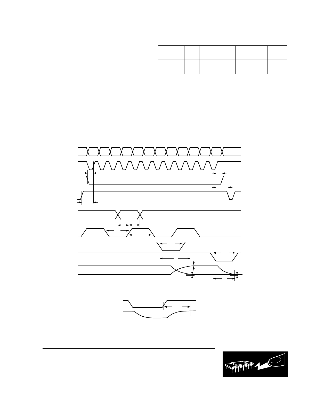
Figure 3. Timing Diagrams
CAUTION
ESD (electrostatic discharge) sensitive device. Electrostatic charges as high as 4000 V readily
accumulate on the human body and test equipment and can discharge without detection.
Although the AD8303 features proprietary ESD protection circuitry, permanent damage may
occur on devices subjected to high energy electrostatic discharges. Therefore, proper ESD
precautions are recommended to avoid performance degradation or loss of functionality.
t
RS
t
S
REV. 0–4–
AD8303
Table I. Control-Logic Truth Table
CS CLK RS MSB SHDN LDA/B Serial Shift Register Function DAC Register Function
H X H X H H No Effect Latched
L L H X H H No Effect Latched
L H H X H H No Effect Latched
L ↑+ H X H H Shift-Register-Data Advanced One Bit Latched
↑+ L H X H H No Effect Latched
HX H X H ↓– No Effect Updated with Current Shift Register Contents
H X H X H L No Effect Transparent
X X L H H X No Effect Loaded with 800
XX ↑+ H H H No Effect Latched with 800
X X L L H X No Effect Loaded with All Zeros
XX ↑+ X H H No Effect Latched All Zeros
X X X X L X No Effect No Effect
NOTES
1
↑+ positive logic transition; ↓– negative logic transition; X Don’t Care.
2
Do not clock in serial data while LDA or LDB is LOW.
PIN DESCRIPTIONS
Pin No. Name Function
1 AGND Analog Ground.
2V
OUTA
DAC voltage output, 2.0475 V full scale with 0.5 mV per bit. An internal temperature stabilized reference
maintains a fixed full-scale voltage independent of time, temperature and power supply variations.
3V
REF
Reference Voltage Output Terminal. Very high output resistance must be buffered if used as a virtual
ground.
4 DGND Digital Ground
5
CS Chip Select, Active Low Input. Disables shift register loading when high. Does not effect LDA or LDB
operation.
6 CLK Clock Input, positive edge clocks data into shift register.
7 SDI Serial Data Input, input data loads directly into the shift register.
8
LDA Load DAC register strobes, active low. Transfers shift register data to DAC A register. Asynchronous active
low input. See Control Logic Truth Table for operation.
9
10
RS Resets DAC register to zero condition or half-scale depending on MSB pin. Asynchronous active low input.
LDB Load DAC register strobes, active low. Transfers shift register data to DAC B register. Asynchronous active
low input. See Control Logic Truth Table for operation.
11 MSB Digital Input: Logic High presets DAC registers to half-scale 800
12
13 V
14 V
is strobed; Logic Low clears all DAC registers to zero (000
SHDN Active low shutdown control input. Does not affect register contents as long as power is present on VDD.
DD
OUTB
Positive power supply input. Specified range of operation +2.7 V to +5.5 V
DAC voltage output, 2.0475 V full scale with 0.5 mV per bit. An internal temperature stabilized reference
H
(sets MSB bit to one) when the RS pin
H
) when the RS pin is strobed.
maintains a fixed full-scale voltage independent of time, temperature and power supply variations.
H
H
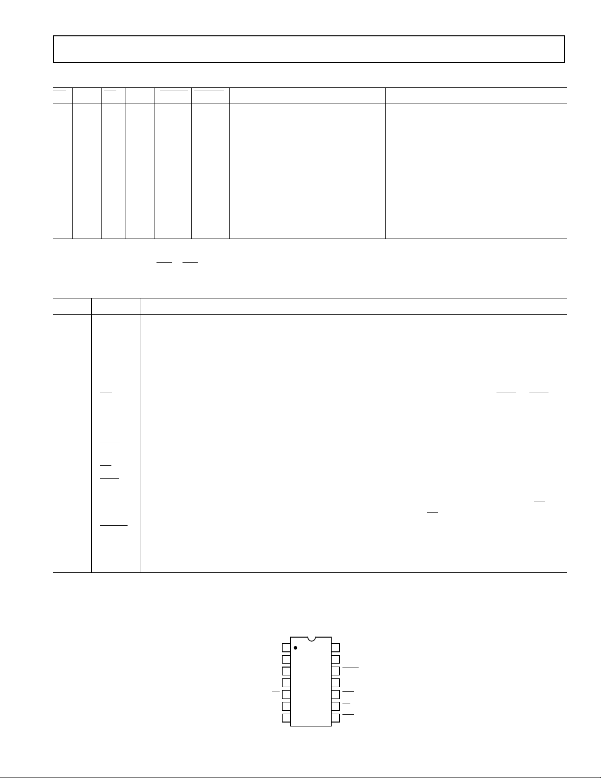
PIN CONFIGURATION
14-Pin P-DIP (N-14)
14-Lead SOIC (R-14)
1
AGND
V
2
OUTA
V
3
REF
AD8303
TOP VIEW
4
DGND
CLK
SDI
CS
(Not to Scale)
5
6
7
REV. 0 –5–
14
V
OUTB
13
V
DD
SHDN
12
11
MSB
10
LDB
9
RS
LDA
8
 Loading...