Analog Devices AD8302 a Datasheet
LF–2.7 GHz
MFLT
VMAG
MSET
PSET
VPHS
PFLT
VREF
VIDEO OUTPUT – A
INPA
OFSA
COMM
OFSB
INPB
VPOS
+
–+–
60dB LOG AMPS
(7 DETECTORS)
60dB LOG AMPS
(7 DETECTORS)
VIDEO OUTPUT – B
PHASE
DETECTOR
+
–
BIAS
x3
1.8V
AD8302
a
FEATURES
Measures Gain/Loss and Phase up to 2.7 GHz
Dual Demodulating Log Amps and Phase Detector
Input Range –60 dBm to 0 dBm in a 50 ⍀ System
Accurate Gain Measurement Scaling (30 mV/dB)
Typical Nonlinearity < 0.5 dB
Accurate Phase Measurement Scaling (10 mV/Degree)
Typical Nonlinearity < 1 Degree
Measurement/Controller/Level Comparator Modes
Operates from Supply Voltages of 2.7 V–5.5 V
Stable 1.8 V Reference Voltage Output
Small Signal Envelope Bandwidth from DC to 30 MHz
APPLICATIONS
RF/IF PA Linearization
Precise RF Power Control
Remote System Monitoring and Diagnostics
Return Loss/VSWR Measurements
Log Ratio Function for AC Signals
RF/IF Gain and Phase Detector
AD8302
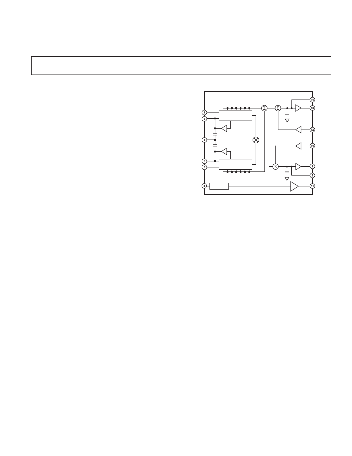
FUNCTIONAL BLOCK DIAGRAM
PRODUCT DESCRIPTION
The AD8302 is a fully integrated system for measuring gain/loss
and phase in numerous receive, transmit, and instrumentation
applications. It requires few external components and a single
supply of 2.7 V–5.5 V. The ac-coupled input signals can range
from –60 dBm to 0 dBm in a 50 Ω system, from low frequencies
up to 2.7 GHz. The outputs provide an accurate measurement
of either gain or loss over a ±30 dB range scaled to 30 mV/dB,
and of phase over a 0°–180° range scaled to 10 mV/degree.
Both subsystems have an output bandwidth of 30 MHz, which
may optionally be reduced by the addition of external filter
capacitors. The AD8302 can be used in controller mode to
force
the gain and phase of a signal chain toward predetermined
setpoints.
The AD8302 comprises a closely matched pair of demodulating
logarithmic amplifiers, each having a 60 dB measurement range.
By taking the difference of their outputs, a measurement of
the magnitude ratio or gain between the two input signals is
available. These signals may even be at different frequencies,
allowing the measurement of conversion gain or loss. The AD8302
may be used to determine absolute signal level by applying the
unknown signal to one input and a calibrated ac reference signal
to the other. With the output stage feedback connection disabled, a comparator may be realized, using the setpoint pins
MSET and PSET to program the thresholds.
The signal inputs are single-ended, allowing them to be matched
and connected directly to a directional coupler. Their input
impedance is nominally 3 kΩ at low frequencies.
The AD8302 includes a phase detector of the multiplier type,
but with precise phase balance driven by the fully limited signals
appearing at the outputs of the two logarithmic amplifiers.
Thus, the phase accuracy measurement is independent of signal
level over a wide range.
The phase and gain output voltages are simultaneously available
at loadable ground referenced outputs over the standard output
range of 0 V to 1.8 V. The output drivers can source or sink up
to 8 mA. A loadable, stable reference voltage of 1.8 V is available for precise repositioning of the output range by the user.
In controller applications, the connection between the gain
output pin VMAG and the setpoint control pin MSET is broken.
The desired setpoint is presented to MSET and the VMAG
control signal drives an appropriate external variable gain device.
Likewise, the feedback path between the phase output pin VPHS
and its setpoint control pin PSET may be broken to allow
operation as a phase controller.
The AD8302 is fabricated on Analog Devices’ proprietary, high
performance 25 GHz SOI complementary bipolar IC process. It is
available in a 14-lead TSSOP package and operates over a –40°C
to +85°C temperature range. An evaluation board is available.
REV. A
Information furnished by Analog Devices is believed to be accurate and
reliable. However, no responsibility is assumed by Analog Devices for its
use, nor for any infringements of patents or other rights of third parties that
may result from its use. No license is granted by implication or otherwise
under any patent or patent rights of Analog Devices.
One Technology Way, P.O. Box 9106, Norwood, MA 02062-9106, U.S.A.
Tel: 781/329–4700 www.analog.com
Fax: 781/326-8703 © Analog Devices, Inc., 2002

AD8302–SPECIFICATIONS
resistors connected to INPA and INPB, for Phase measurement P
(TA = 25ⴗC, VS = 5 V, VMAG shorted to MSET, VPHS shorted to PSET, 52.3 ⍀ shunt
= P
INPA
, unless otherwise noted.)
INPB
Parameter Conditions Min Typ Max Unit
OVERALL FUNCTION
Input Frequency Range >0 2700 MHz
Gain Measurement Range P
Phase Measurement Range φ
at INPA, PIN at INPB = –30 dBm ± 30 dB
IN
at INPA > φIN at INPB ± 90 Degree
IN
Reference Voltage Output Pin VREF, –40°C ≤ TA ≤ +85°C 1.72 1.8 1.88 V
INPUT INTERFACE Pins INPA and INPB
Input Simplified Equivalent Circuit To AC Ground, f ≤ 500 MHz 3储2kΩ储pF
Input Voltage Range AC-Coupled (0 dBV = 1 V rms) –73 –13 dBV
re: 50 Ω –60 0 dBm
Center of Input Dynamic Range –43 dBV
–30 dBm
MAGNITUDE OUTPUT Pin VMAG
Output Voltage Minimum 20 × Log (V
Output Voltage Maximum 20 × Log (V
Center Point of Output (MCP) V
INPA
= V
INPB
INPA/VINPB
INPA/VINPB
) = –30 dB 30 mV
) = +30 dB 1.8 V
900 mV
Output Current Source/Sink 8 mA
Small Signal Envelope Bandwidth Pin MFLT Open 30 MHz
Slew Rate 40 dB Change, Load 20 pF储10 kΩ 25 V/µs
Response Time
Rise Time Any 20 dB Change, 10%–90% 50 ns
Fall Time Any 20 dB Change, 90%–10% 60 ns
Settling Time Full-Scale 60 dB Change, to 1% Settling 300 ns
PHASE OUTPUT Pin VPHS
Output Voltage Minimum Phase Difference 180 Degrees 30 mV
Output Voltage Maximum Phase Difference 0 Degrees 1.8 V
= φ
Phase Center Point When φ
INPA
± 90° 900 mV
INPB
Output Current Drive Source/Sink 8 mA
Slew Rate 25 V/µs
Small Signal Envelope Bandwidth 30 MHz
Response Time Any 15 Degree Change, 10%–90% 40 ns
120 Degree Change C
= 1 pF, to 1% Settling 500 ns
FILT
100 MHz MAGNITUDE OUTPUT
Dynamic Range ± 1 dB Linearity P
± 0.5 dB Linearity P
± 0.2 dB Linearity P
= –30 dBm (V
REF
= –30 dBm (V
REF
= –30 dBm (V
REF
= –43 dBV) 58 dB
REF
= –43 dBV) 55 dB
REF
= –43 dBV) 42 dB
REF
Slope From Linear Regression 29 mV/dB
Deviation vs. Temperature Deviation from Output at 25°C
–40°C ≤ T
≤ +85°C, P
A
INPA
= P
= –30 dBm 0.25 dB
INPB
Deviation from Best Fit Curve at 25°C
Gain Measurement Balance P
–40°C ≤ T
= P
INPA
≤ +85°C, P
A
= –5 dBm to –50 dBm 0.2 dB
INPB
= ± 25 dB, P
INPA
= –30 dBm 0.25 dB
INPB
PHASE OUTPUT
Dynamic Range Less than ± 1 Degree Deviation from Best Fit Line 145 Degree
Less than 10% Deviation in Instantaneous Slope 143 Degree
Slope (Absolute Value) From Linear Regression about –90° or +90° 10 mV/Degree
Deviation vs. Temperature Deviation from Output at 25°C
–40°C ≤ T
≤ +85°C, Delta Phase = 90 Degrees 0.7 Degree
A
Deviation from Best Fit Curve at 25°C
–40°C ≤ TA ≤ +85°C, Delta Phase = ± 30 Degrees 0.7 Degree
–2–
REV. A

AD8302
Parameter Conditions Min Typ Max Unit
900 MHz MAGNITUDE OUTPUT
Dynamic Range ± 1 dB Linearity P
± 0.5 dB Linearity P
± 0.2 dB Linearity P
Slope From Linear Regression 28.7 mV/dB
Deviation vs. Temperature Deviation from Output at 25°C
–40°C ≤ T
≤ +85°C, P
A
Deviation from Best Fit Curve at 25°C
Gain Measurement Balance P
–40°C ≤ T
INPA
= P
≤ +85°C, P
A
INPB
PHASE OUTPUT
Dynamic Range Less than ± 1 Degree Deviation from Best Fit Line 143 Degree
Less than 10% Deviation in Instantaneous Slope 143 Degree
Slope (Absolute Value) From Linear Regression about –90° or +90° 10.1 mV/Degree
Deviation Linear Deviation from Best Fit Curve at 25°C
–40°C ≤ T
–40°C ≤ T
≤ +85°C, Delta Phase = 90 Degrees 0.75 Degree
A
≤ +85°C, Delta Phase = ± 30 Degrees 0.75 Degree
A
Phase Measurement Balance Phase @ INPA = Phase @ INPB, PIN = –5 dBm to –50 dBm 0.8
1900 MHz MAGNITUDE OUTPUT
Dynamic Range ± 1 dB Linearity P
± 0.5 dB Linearity P
± 0.2 dB Linearity P
Slope From Linear Regression 27.5 mV/dB
Deviation vs. Temperature Deviation from Output at 25°C
–40°C ≤ T
≤ +85°C, P
A
Deviation from Best Fit Curve at 25°C
Gain Measurement Balance P
–40°C ≤ T
INPA
= P
≤ +85°C, P
A
INPB
PHASE OUTPUT
Dynamic Range Less than ± 1 Degree Deviation from Best Fit Line 128 Degree
Less than 10% Deviation in Instantaneous Slope 120 Degree
Slope (Absolute Value) From Linear Regression about –90° or +90° 10.2 mV/Degree
Deviation Linear Deviation from Best Fit Curve at 25°C
–40°C ≤ T
–40°C ≤ T
≤ +85°C, Delta Phase = 90 Degrees 0.8 Degree
A
≤ +85°C, Delta Phase = ± 30 Degrees 0.8 Degree
A
Phase Measurement Balance Phase @ INPA = Phase @ INPB, PIN = –5 dBm to –50 dBm 1 Degree
2200 MHz MAGNITUDE OUTPUT
Dynamic Range ± 1 dB Linearity P
± 0.5 dB Linearity P
± 0.2 dB Linearity P
Slope From Linear Regression 27.5 mV/dB
Deviation vs. Temperature Deviation from Output at 25°C
–40°C ≤ T
≤ +85°C, P
A
Deviation from Best Fit Curve at 25°C
Gain Measurement Balance P
–40°C ≤ T
INPA
= P
≤ +85°C, P
A
INPB
PHASE OUTPUT
Dynamic Range Less than ± 1 Degree Deviation from Best Fit Line 115 Degree
Less than 10% Deviation in Instantaneous Slope 110 Degree
Slope (Absolute Value) From Linear Regression about –90° or +90° 10 mV/Degree
Deviation Linear Deviation from Best Fit Curve at 25°C
–40°C ≤ T
≤ +85°C, Delta Phase = 90 Degrees 0.85 Degree
A
–40°C ≤ TA ≤ +85°C, Delta Phase = ± 30 Degrees 0.9 Degree
REFERENCE VOLTAGE Pin VREF
Output Voltage Load = 2 kΩ 1.7 1.8 1.9 V
PSRR V
= 2.7 V to 5.5 V 0.25 mV/V
S
Output Current Source/Sink (Less than 1% Change) 5 mA
POWER SUPPLY Pin VPOS
Supply 2.7 5.0 5.5 V
Operating Current (Quiescent) V
= 5 V 19 25 mA
S
–40°C ≤ TA ≤ +85°C2127mA
Specifications subject to change without notice.
= –30 dBm (V
REF
= –30 dBm (V
REF
= –30 dBm (V
REF
= P
INPA
= ± 25 dB, P
INPA
= –43 dBV) 58 dB
REF
= –43 dBV) 54 dB
REF
= –43 dBV) 42 dB
REF
= –30 dBm 0.25 dB
INPB
= –30 dBm 0.25 dB
INPB
= –5 dBm to –50 dBm 0.2 dB
Degree
= –30 dBm (V
REF
= –30 dBm (V
REF
= –30 dBm (V
REF
= P
INPA
= ±25 dB, P
INPA
= –5 dBm to –50 dBm 0.2 dB
= –30 dBm (V
REF
= –30 dBm (V
REF
= –30 dBm (V
REF
= P
INPA
= ± 25 dB, P
INPA
= –5 dBm to –50 dBm 0.2 dB
= –43 dBV) 57 dB
REF
= –43 dBV) 54 dB
REF
= –43 dBV) 42 dB
REF
= –30 dBm 0.27 dB
INPB
= –30 dBm 0.33 dB
INPB
= –43 dBV) 53 dB
REF
= –43 dBV) 51 dB
REF
= –43 dBV) 38 dB
REF
= –30 dBm 0.28 dB
INPB
= –30 dBm 0.4 dB
INPB
REV. A
–3–
AD8302
TOP VIEW
(Not to Scale)
1
COMM
AD8302
INPA
OFSA
VPOS
OFSB
INPB
COMM
MFLT
VMAG
MSET
VREF
PSET
VPHS
PFLT
2
3
4
5
6
7
14
13
12
11
10
9
8
WARNING!
ESD SENSITIVE DEVICE
ABSOLUTE MAXIMUM RATINGS
1
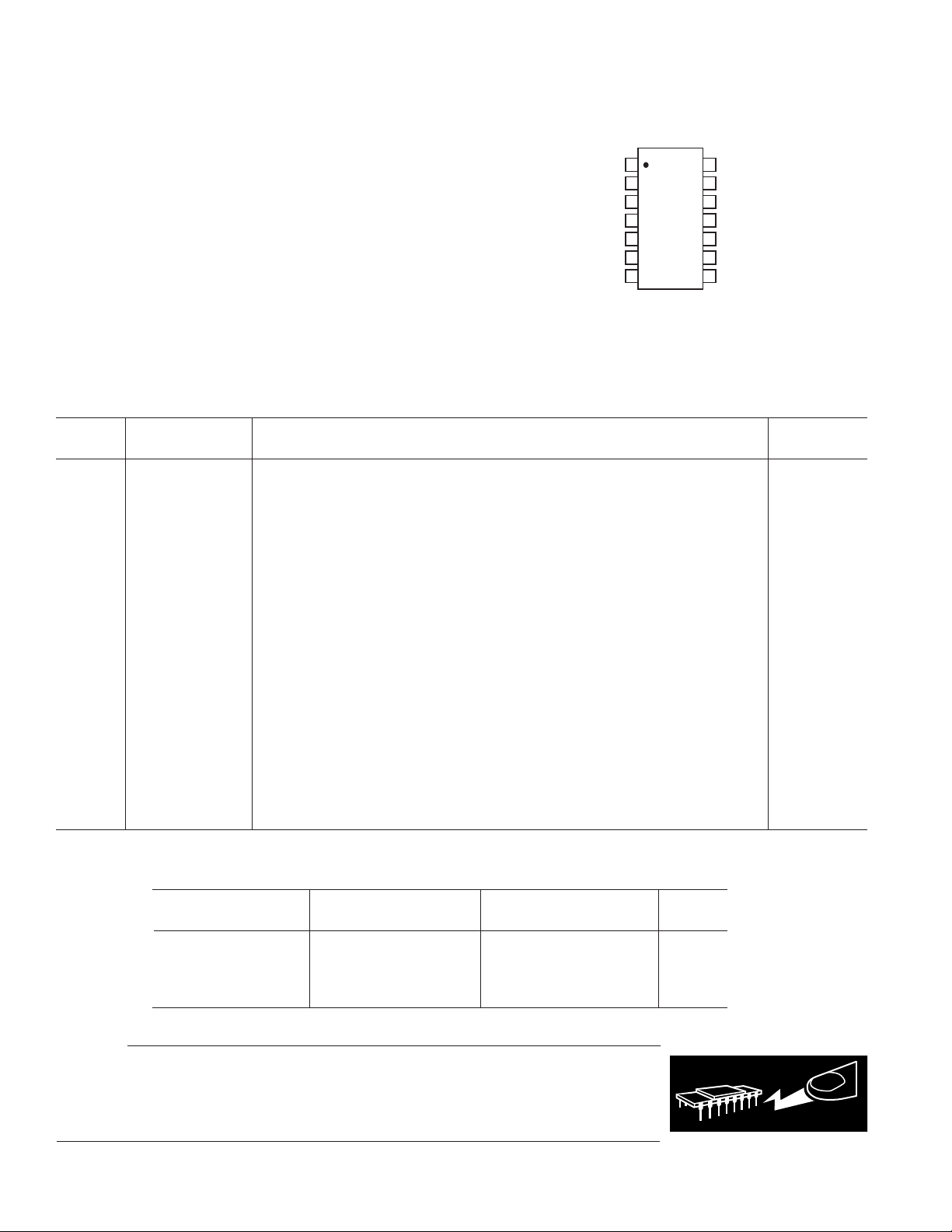
PIN CONFIGURATION
Supply Voltage VS . . . . . . . . . . . . . . . . . . . . . . . . . . . . . 5.5 V
PSET, MSET Voltage . . . . . . . . . . . . . . . . . . . . . . V
+ 0.3 V
S
INPA, INPB Maximum Input . . . . . . . . . . . . . . . . . . –3 dBV
Equivalent Power Re. 50 Ω . . . . . . . . . . . . . . . . . . 10 dBm
2
. . . . . . . . . . . . . . . . . . . . . . . . . . . . . . . . . . . . . 150°C/W
θ
JA
Maximum Junction Temperature . . . . . . . . . . . . . . . . 125°C
Operating Temperature Range . . . . . . . . . . . –40°C to +85°C
Storage Temperature Range . . . . . . . . . . . . –65°C to +150°C
Lead Temperature Range (Soldering 60 sec) . . . . . . . . 300°C
NOTES
1
Stresses above those listed under Absolute Maximum Ratings may cause permanent damage to the device. This is a stress rating only; functional operation of the
device at these or any other conditions above those indicated in the operational
section of this specification is not implied. Exposure to absolute maximum rating
conditions for extended periods may affect device reliability.
2
JEDEC 1S Standard (2-layer) board data.
PIN FUNCTION DESCRIPTIONS
Equivalent
Pin No. Mnemonic Function Circuit
1, 7 COMM Device Common. Connect to low impedance ground.
2 INPA High Input Impedance to Channel A. Must be ac-coupled. Circuit A
3 OFSA A capacitor to ground at this pin sets the offset compensation filter corner Circuit A
and provides input decoupling.
4 VPOS Voltage Supply (V
), 2.7 V to 5.5 V
S
5 OFSB A capacitor to ground at this pin sets the offset compensation filter corner Circuit A
and provides input decoupling.
6 INPB Input to Channel B. Same structure as INPA. Circuit A
8 PFLT Low Pass Filter Terminal for the Phase Output Circuit E
9 VPHS Single-Ended Output Proportional to the Phase Difference between INPA Circuit B
and INPB.
10 PSET Feedback Pin for Scaling of VPHS Output Voltage in Measurement Mode. Circuit D
Apply a setpoint voltage for controller mode.
11 VREF Internally Generated Reference Voltage (1.8 V Nominal) Circuit C
12 MSET Feedback Pin for Scaling of VMAG Output Voltage Measurement Mode. Circuit D
Accepts a set point voltage in controller mode.
13 VMAG Single-Ended Output. Output voltage proportional to the decibel ratio
of signals applied to INPA and INPB. Circuit B
14 MFLT Low Pass Filter Terminal for the Magnitude Output Circuit E
CAUTION
ESD (electrostatic discharge) sensitive device. Electrostatic charges as high as 4000 V readily
accumulate on the human body and test equipment and can discharge without detection. Although
the AD8302 features proprietary ESD protection circuitry, permanent damage may occur on
devices subjected to high energy electrostatic discharges. Therefore, proper ESD precautions are
recommended to avoid performance degradation or loss of functionality.
ORDERING GUIDE
Package
Model Temperature Range Package Description Option
AD8302ARU –40°C to +85°C Tube, 14-Lead TSSOP RU-14
AD8302ARU-REEL 13" Tape and Reel
AD8302ARU-REEL7 7" Tape and Reel
AD8302-EVAL Evaluation Board
–4–
REV. A
AD8302
INPA(INPB)
OFSA(OFSB)
VPOS
COMM
10k⍀
5k⍀
Circuit C
100mV
4k⍀
4k⍀
10pF
COMM
Circuit A
VREF
VPOS
+
ON TO
LOG-AMP
–
MSET
(PSET)
VPOS
10k⍀
10k⍀
COMM
Circuit D
ACTIVE LOADS
750⍀
2k⍀
VPOS
CLASS A-B
CONTROL
COMM
Circuit B
25⍀
VPOS
COMM
Circuit E
VMAG
(VPHS)
MFLT
(PFLT)
1.5pF
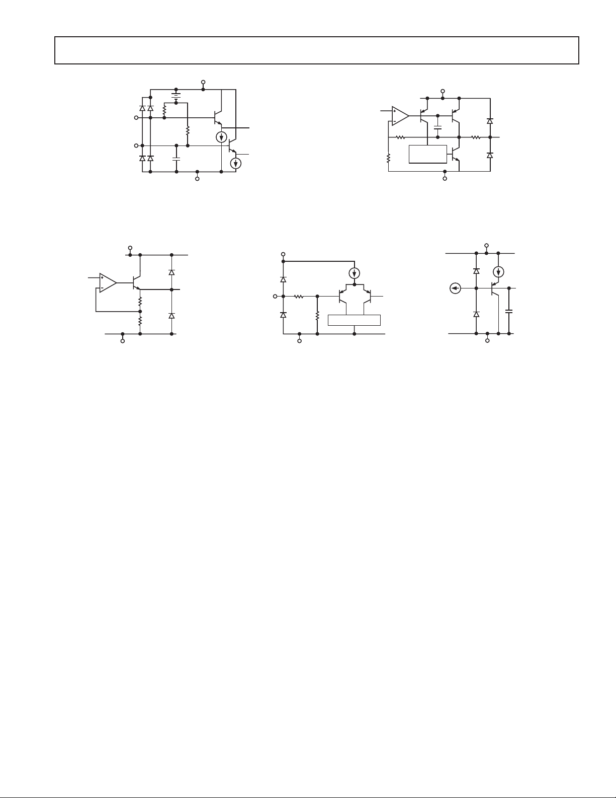
Figure 1. Equivalent Circuits
REV. A
–5–
AD8302
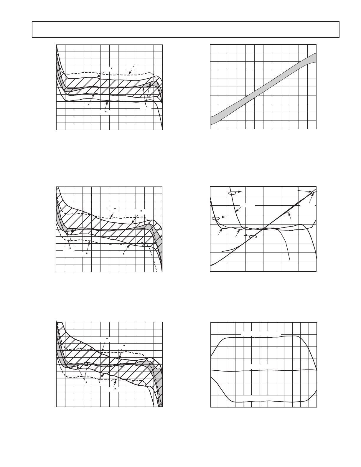
MAGNITUDE RATIO – dB
–30
VMAG – V
–20 –10 0 10 20 30
3.0
ERROR IN VMAG – dB
2.5
2.0
1.5
1.0
0.5
0.0
–0.5
–1.0
–1.5
–3.0
–2.0
–2.5
1.80
1.65
0
1.50
1.35
1.20
1.05
0.90
0.75
0.60
0.45
0.30
0.15
+25ⴗC
+85ⴗC
–40ⴗC
(VS = 5 V, V
–Typical Performance Characteristics
is the reference input and V
INPB
is swept, unless otherwise noted. All references to dBm are referred to 50 ⍀. For the phase output
INPA
curves, the input signal levels are equal, unless otherwise noted.)
2.0
1.8
1.6
1.4
1.2
1.0
VMAG – V
0.8
0.6
0.4
0.2
0
–30
–25 –20 –15 –10 –5 0 5 1015202530
MAGNITUDE RATIO – dB
100
2700
900
2200
1900
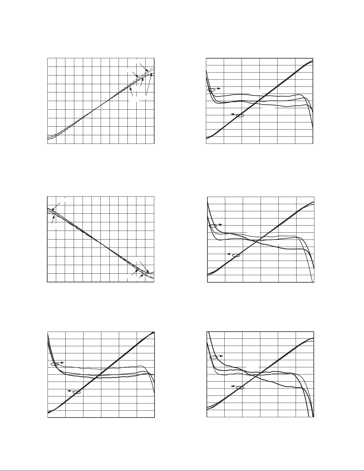
TPC 1. Magnitude Output (VMAG) vs. Input Level Ratio
(Gain) V
INPA/VINPB
1900 MHz, 2200 MHz, 2700 MHz, 25
Ω
(Re: 50
)
2.0
1.8
1.6
1.4
1.2
1.0
VMAG – V
0.8
0.6
0.4
0.2
0
–30
TPC 2. VMAG vs. Input Level Ratio (Gain) V
, Frequencies 100 MHz, 900 MHz,
ⴗ
C, P
1900
2700
–25 –20 –15 –10 –5 0 5 1015202530
MAGNITUDE RATIO – dB
= –30 dBm,
INPB
2200
900
100
INPA/VINPB
,
Frequencies 100 MHz, 900 MHz, 1900 MHz, 2200 MHz,
2700 MHz, P
= –30 dBm
INPA
1.80
1.65
1.50
1.35
1.20
1.05
0.90
0.75
VMAG – V
0.60
0.45
0.30
0.15
0
–30
–20 –10 0 10 20 30
–40ⴗC
+25ⴗC
+85ⴗC
MAGNITUDE RATIO – dB
3.0
2.5
2.0
1.5
1.0
0.5
0.0
–0.5
–1.0
–1.5
–2.0
–2.5
–3.0
ERROR IN VMAG – dB
TPC 4. VMAG and Log Conformance vs. Input Level Ratio
ⴗ
(Gain), Frequency 900 MHz, –40
C, +25ⴗC, and +85ⴗC,
Reference Level = –30 dBm
1.80
1.65
1.50
1.35
1.20
1.05
0.90
0.75
VMAG – V
0.60
0.45
0.30
0.15
0
–30
–20 –10 0 10 20 30
–40ⴗC
+25ⴗC
+85ⴗC
MAGNITUDE RATIO – dB
3.0
2.5
2.0
1.5
1.0
0.5
0.0
–0.5
–1.0
–1.5
–2.0
–2.5
–3.0
ERROR IN VMAG – dB
TPC 5. VMAG and Log Conformance vs. Input Level Ratio
ⴗ
(Gain), Frequency 1900 MHz, –40
C, +25ⴗC, and +85ⴗC,
Reference Level = –30 dBm
1.80
1.65
1.50
1.35
1.20
1.05
0.90
VMAG – V
0.75
0.60
0.45
0.30
0.15
0
–30
–20 –100 102030
TPC 3. VMAG Output and Log Conformance vs. Input
Level Ratio (Gain), Frequency 100 MHz, –40
ⴗ
and +85
C, Reference Level = –30 dBm
–40ⴗC
MAGNITUDE RATIO – dB
+85ⴗC
+25ⴗC
ⴗ
C, +25ⴗC,
3.0
2.5
2.0
1.5
1.0
0.5
0.0
–0.5
–1.0
–1.5
–2.0
–2.5
–3.0
ERROR IN VMAG – dB
TPC 6. VMAG Output and Log Conformance vs. Input
Level Ratio (Gain), Frequency 2200 MHz, –40
ⴗ
and +85
C, Reference Level = –30 dBm
–6–
ⴗ
C, +25ⴗC,
REV. A
AD8302
3.0
2.5
2.0
1.5
1.0
0.5
0.0
–0.5
–1.0
ERROR IN VMAG – dB
–1.5
–2.0
–2.5
–3.0
–25 –20 –15 –10 –5 0 5 1015202530
–30
+85 C
+85 C
–40 C
MAGNITUDE RATIO – dB
–40 C
+25 C
TPC 7. Distribution of Magnitude Error vs. Input Level
Ratio (Gain), Three Sigma to Either Side of Mean,
ⴗ
Frequency 900 MHz, –40
C, +25ⴗC, and +85ⴗC, Refer-
ence Level = –30 dBm
3.0
2.5
2.0
1.5
1.0
0.5
0.0
–0.5
–1.0
ERROR IN VMAG – dB
+25 C
–1.5
–2.0
–2.5
–3.0
–25 –20 –15 –10 –5 0 5 1015202530
–30
–40 C
MAGNITUDE RATIO – dB
–40 C
+85 C
+85 C
TPC 8. Distribution of Error vs. Input Level Ratio (Gain),
Three Sigma to Either Side of Mean, Frequency 1900 MHz,
ⴗ
C, +25ⴗC, and +85ⴗC, Reference Level = –30 dBm
–40
2.0
1.8
1.6
1.4
1.2
1.0
VMAG – V
0.8
0.6
0.4
0.2
0.0
–30
–25 –20 –15 –10 –5 0 5 1015202530
MAGNITUDE RATIO – dB
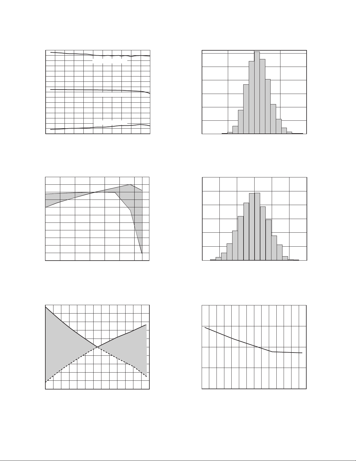
TPC 10. Distribution of VMAG vs. Input Level Ratio (Gain),
Three Sigma to Either Side of Mean, Frequency 1900 MHz,
ⴗ
Temperatures Between –40
C and +85ⴗC, Reference Level
= –30 dBm
–30dBm
3.0
2.5
2.0
1.5
1.0
0.5
0.0
–0.5
–1.0
–1.5
–2.0
–2.5
–3.0
ERROR IN VMAG – dB
1.8
1.6
1.4
1.2
1.0
0.8
VMAG – V
–30dBm
0.6
0.4
0.2
0.0
–30
–45dBm
–15dBm
–20 –100 102030
MAGNITUDE RATIO – dB
–45dBm
–15dBm
TPC 11. VMAG Output and Log Conformance vs. Input
Level Ratio (Gain), Reference Level = –15 dBm, –30 dBm,
and –45 dBm, Frequency 1900 MHz
3.0
2.5
2.0
1.5
1.0
0.5
0.0
–0.5
–1.0
ERROR IN VMAG – dB
–1.5
–2.0
–2.5
–3.0
–30
+25 C
–25 –20 –15 –10 –5 0 5 1015202530
–40 C
+85 C
+85 C
–40 C
MAGNITUDE RATIO – dB
TPC 9. Distribution of Magnitude Error vs. Input Level
Ratio (Gain), Three Sigma to Either Side of Mean,
Frequency 2200 MHz, Temperatures –40ⴗC, +25ⴗC, and
ⴗ
C, Reference Level = –30 dBm
+85
REV. A
1.10
P
= P
+ 5dB
INPB
1.05
1.00
0.95
0.90
VMAG – V
0.85
0.80
0.75
–65
–60 –55 –50 –45 –40 –35 –30
INPA
P
= P
INPA
INPB
P
= P
INPB
– 5dB
INPA
INPUT LEVEL – dBm
–25 –20 –15 –10 –50
TPC 12. VMAG Output vs. Input Level for P
= P
P
INPA
+ 5 dB, P
INPB
INPA
= P
– 5 dB, Frequency 1900 MHz
INPB
–7–
INPA
= P
INPB
,
AD8302
1.06
1.04
1.02
1.00
0.98
0.96
0.94
0.92
0.90
0.88
VMAG – V
0.86
0.84
0.82
0.80
0.78
0.76
0.74
200 400 600 800 1000 1200 1400
TPC 13. VMAG Output vs. Frequency, for P
= P
+ 5 dB, and P
INPB
0.4
0.2
0
–0.2
–0.4
–0.6
–0.8
–1.0
–1.2
CHANGE IN SLOPE – mV
–1.4
–1.6
–1.8
–40 –200 20406080
INPA
P
= P
INPA
P
INPA
P
= P
INPA
FREQUENCY – MHz
= P
– 5 dB, P
INPB
TEMPERATURE – ⴗC
INPB
= P
INPB
+ 5dB
INPB
– 5dB
1600 1800 2000 22000
INPB
= P
INPA
INPB
= –30 dBm
85
, P
INPA
TPC 14. Change in VMAG Slope vs. Temperature, Three
Sigma to Either Side of Mean, Frequencies 1900 MHz
18
15
12
9
PERCENT
6
3
0
0.80 0.85 0.90
MCP – V
0.95
1.00
TPC 16. Center Point of Magnitude Output (MCP)
Distribution Frequencies 900 MHz, 17,000 Units
18
15
12
9
PERCENT
6
3
0
27.0 27.5 28.0 28.5
VMAG SLOPE – mV/dB
29.0
29.5 30.0
TPC 17. VMAG Slope, Frequency 900 MHz, 17,000 Units
25
20
15
10
5
0
–5
VMAG – mV
–10
–15
–20
–25
–40 –30 –20 –10 0 10 20
TEMPERATURE – ⴗC
30 40 50 60
70 80 90
TPC 15. Change in Center Point of Magnitude Output
(MCP) vs. Temperature, Three Sigma to Either Side of
Mean, Frequencies 1900 MHz
–8–
0.032
0.030
0.028
SLOPE OF VMAG – V
0.026
0.024
0
200
400
600
800
1000
1200
1400
FREQUENCY – MHz
TPC 18. VMAG Slope vs. Frequency
1600
1800
2000
2200
2400
2600
2800
REV. A
 Loading...