Analog Devices AD8300 a Datasheet

+3 Volt, Serial Input
a
FEATURES
Complete 12-Bit DAC
No External Components
Single +3 Volt Operation
0.5 mV/Bit with 2.0475 V Full Scale
6 s Output Voltage Settling Time
Low Power: 3.6 mW
Compact SO-8 1.5 mm Height Package
APPLICATIONS
Portable Communications
Digitally Controlled Calibration
Servo Controls
PC Peripherals
GENERAL DESCRIPTION
The AD8300 is a complete 12-bit, voltage-output digital-toanalog converter designed to operate from a single +3 volt supply. Built using a CBCMOS process, this monolithic DAC
offers the user low cost, and ease-of-use in single-supply +3 volt
systems. Operation is guaranteed over the supply voltage range
of +2.7 V to +5.5 V making this device ideal for battery operated applications.
The 2.0475 V full-scale voltage output is laser trimmed to
maintain accuracy over the operating temperature range of the
device. The binary input data format provides an easy-to-use
one-half-millivolt-per-bit software programmability. The voltage
outputs are capable of sourcing 5 mA.
Complete 12-Bit DAC
AD8300
FUNCTIONAL BLOCK DIAGRAM
12-BIT
CLR
LD
CS
CLK
SDI
REF
EN
DAC
12
DAC
REGISTER
12
SERIAL
REGISTER
AD8300
A double buffered serial data interface offers high speed, threewire, DSP and microcontroller compatible inputs using data in
(SDI), clock (CLK) and load strobe (LD) pins. A chip select
(CS) pin simplifies connection of multiple DAC packages by
enabling the clock input when active low. Additionally, a CLR
input sets the output to zero scale at power on or upon user
demand.
The AD8300 is specified over the extended industrial (–40°C to
+85°C) temperature range. AD8300s are available in plastic
DIP, and low profile 1.5 mm height SO-8 surface mount packages.
V
OUT
V
DD
GND
3.0
DVFS 1 LSB
2.8
DATA = FFF
TA = +258C
2.6
PROPER OPERATION
2.4
WHEN VDD SUPPLY
VOLTAGE ABOVE
2.2
MINIMUM SUPPLY VOLTAGE – Volts
2.0
0.01 100.1 1.0
OUTPUT LOAD CURRENT – mA
H
CURVE
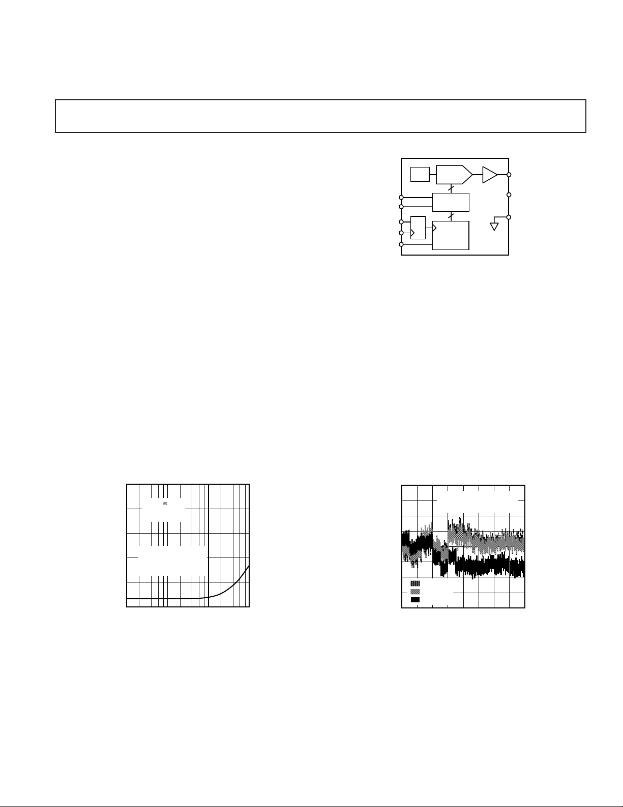
Figure 1. Minimum Supply Voltage vs. Load
REV. A
Information furnished by Analog Devices is believed to be accurate and
reliable. However, no responsibility is assumed by Analog Devices for its
use, nor for any infringements of patents or other rights of third parties
which may result from its use. No license is granted by implication or
otherwise under any patent or patent rights of Analog Devices.
1.00
V
= +2.7V
0.75
0.50
0.25
0.00
–0.25
–0.50
INL LINEARITY ERROR – LSB
–0.75
–1.00
0 40961024 2048
DD
T
= –408C, +258C, +1258C
A
= –408C
= +258C
= +1258C
DIGITAL INPUT CODE – Decimal
3072
Figure 2. Linearity Error vs. Digital Code and Temperature
One Technology Way, P.O. Box 9106, Norwood, MA 02062-9106, U.S.A.
Tel: 781/329-4700 World Wide Web Site: http://www.analog.com
Fax: 781/326-8703 © Analog Devices, Inc., 1999

AD8300–SPECIFICATIONS
+3 V OPERATION
(@ V
= +5 V ⴞ 10%, –40ⴗC ≤ TA ≤ +85ⴗC, unless otherwise noted)
DD
Parameter Symbol Condition Min Typ Max Units
STATIC PERFORMANCE
Resolution N [Note 1] 12 Bits
Relative Accuracy INL –2 ±1/2 +2 LSB
Differential Nonlinearity
Zero-Scale Error V
Full-Scale Voltage
Full-Scale Tempco TCV
2
3
DNL Monotonic –1 ±1/2 +1 LSB
ZSE
V
FS
FS
Data = 000
Data = FFF
H
H
[Notes 3, 4] 16 ppm/°C
+1/2 +3 mV
2.039 2.0475 2.056 Volts
ANALOG OUTPUT
Output Current (Source) I
Output Current (Sink) I
Load Regulation L
Output Resistance to GND R
Capacitive Load C
OUT
OUT
REG
OUT
L
Data = 800
Data = 800
R
= 200 Ω to ∞, Data = 800
L
Data = 000
No Oscillation
H
H
H
, ∆V
, ∆V
4
= 5 LSB 5 mA
OUT
= 5 LSB 2 mA
OUT
H
1.5 5 LSB
30 Ω
500 pF
LOGIC INPUTS
Logic Input Low Voltage V
Logic Input High Voltage V
Input Leakage Current I
Input Capacitance C
INTERFACE TIMING
SPECIFICATIONS
4, 5
Clock Width High t
Clock Width Low t
Load Pulsewidth t
Data Setup t
Data Hold t
Clear Pulsewidth t
Load Setup t
Load Hold t
Select t
Deselect t
AC CHARACTERISTICS
4
Voltage Output Settling Time t
IL
IH
IL
IL
CH
CL
LDW
DS
DH
CLRW
LD1
LD2
CSS
CSH
S
To ±0.2% of Full Scale 7 µs
To ±1 LSB of Final Value
Output Slew Rate SR Data = 000
to FFFH to 000
H
2.1 V
40 ns
40 ns
50 ns
15 ns
15 ns
40 ns
15 ns
40 ns
40 ns
40 ns
6
H
14 µs
2.0 V/µs
0.6 V
10 µA
10 pF
DAC Glitch 15 nV/s
Digital Feedthrough 15 nV/s
SUPPLY CHARACTERISTICS
Power Supply Range VDD
Positive Supply Current I
Power Dissipation P
DD
DISS
RANGE
DNL < ±1 LSB 2.7 5.5 V
VDD = 3 V, VIL = 0 V, Data = 000
V
= 3.6 V, VIH = 2.3 V, Data = FFF
DD
VDD = 3 V, VIL = 0 V, Data = 000
H
H
H
1.2 1.7 mA
1.9 3.0 mA
3.6 5.1 mW
Power Supply Sensitivity PSS ∆VDD = ±5% 0.001 0.005 %/%
NOTES
1
LSB = 0.5 mV for 0 V to +2.0475 V output range.
2
The first two codes (000H, 001H) are excluded from the linearity error measurement.
3
Includes internal voltage reference error.
4
These parameters are guaranteed by design and not subject to production testing.
5
All input control signals are specified with tR = tF = 2 ns (10% to 90% of +3 V) and timed from a voltage level of 1.6 V.
6
The settling time specification does not apply for negative going transitions within the last 6 LSBs of ground. Some devices exhibit double the typical settling time in
this 6 LSB region.
Specifications subject to change without notice.
–2–
REV. A

AD8300
+5 V OPERATION
(@ V
= +5 V ⴞ 10%, –40ⴗC ≤ TA ≤ +85ⴗC, unless otherwise noted)
DD
Parameter Symbol Condition Min Typ Max Units
STATIC PERFORMANCE
Resolution N [Note 1] 12 Bits
Relative Accuracy INL –2 ±1/2 +2 LSB
Differential Nonlinearity
Zero-Scale Error V
Full-Scale Voltage
Full-Scale Tempco TCV
2
3
DNL Monotonic –1 ±1/2 +1 LSB
ZSE
V
FS
FS
Data = 000
Data = FFF
H
H
[Notes 3, 4] 16 ppm/°C
+1/2 +3 mV
2.039 2.0475 2.056 Volts
ANALOG OUTPUT
Output Current (Source) I
Output Current (Sink) I
Load Regulation L
Output Resistance to GND R
Capacitive Load C
OUT
OUT
REG
OUT
L
Data = 800
Data = 800
R
= 200 Ω to ∞, Data = 800
L
Data = 000
No Oscillation
H
H
H
, ∆V
, ∆V
4
= 5 LSB 5 mA
OUT
= 5 LSB 2 mA
OUT
H
1.5 5 LSB
30 Ω
500 pF
LOGIC INPUTS
Logic Input Low Voltage V
Logic Input High Voltage V
Input Leakage Current I
Input Capacitance C
INTERFACE TIMING
SPECIFICATIONS
4, 5
Clock Width High t
Clock Width Low t
Load Pulsewidth t
Data Setup t
Data Hold t
Clear Pulsewidth t
Load Setup t
Load Hold t
Select t
Deselect t
AC CHARACTERISTICS
4
Voltage Output Settling Time t
IL
IH
IL
IL
CH
CL
LDW
DS
DH
CLWR
LD1
LD2
CSS
CSH
S
To ±0.2% of Full Scale 6 µs
To ±1 LSB of Final Value
Output Slew Rate SR Data = 000
to FFFH to 000
H
2.4 V
30 ns
30 ns
30 ns
15 ns
15 ns
30 ns
15 ns
30 ns
30 ns
30 ns
6
H
13 µs
2.2 V/µs
0.8 V
10 µA
10 pF
DAC Glitch 15 nV/s
Digital Feedthrough 15 nV/s
SUPPLY CHARACTERISTICS
Power Supply Range VDD
Positive Supply Current I
Power Dissipation P
DD
DISS
RANGE
DNL < ±1 LSB 2.7 5.5 V
VDD = 5 V, VIL = 0 V, Data = 000
V
= 5.5 V, VIH = 2.3 V, Data = FFF
DD
VDD = 5 V, VIL = 0 V, Data = 000
H
H
H
1.2 1.7 mA
2.8 4.0 mA
6 5.1 mW
Power Supply Sensitivity PSS ∆VDD = ±10% 0.001 0.006 %/%
NOTES
1
1 LSB = 0.5 mV for 0 V to +2.0475 V output range.
2
The first two codes (000H, 001H) are excluded from the linearity error measurement.
3
Includes internal voltage reference error.
4
These parameters are guaranteed by design and not subject to production testing.
5
All input control signals are specified with tR = tF = 2 ns (10% to 90% of +5 V) and timed from a voltage level of 1.6 V.
6
The settling time specification does not apply for negative going transitions within the last 6 LSBs of ground. Some devices exhibit double the typical settling time in
this 6 LSB region.
Specifications subject to change without notice.
REV. A –3–
 Loading...