

Single Supply, Low Power
a
FEATURES
Low Cost
Three Video Amplifiers in One Package
Optimized for Driving Cables in Video Systems
Excellent Video Specifications (RL = 150 V)
Gain Flatness 0.1 dB to 50 MHz
0.03% Differential Gain Error
0.068 Differential Phase Error
Low Power
Operates on Single +3 V to 615 V Power Supplies
5.5 mA/Amplifier Max Power Supply Current
High Speed
125 MHz Unity Gain Bandwidth (–3 dB)
500 V/ms Slew Rate
High Speed Disable Function per Channel
Turn-Off Time 80 ns
Easy to Use
50 mA Output Current
Output Swing to 1 V of Rails
APPLICATIONS
Video Line Driver
LCD Drivers
Computer Video Plug-In Boards
Ultrasound
RGB Amplifier
CCD Based Systems
PRODUCT DESCRIPTION
The AD813 is a low power, single supply triple video amplifier.
Each of the three current feedback amplifiers has 50 mA of output
current, and is optimized for driving one back-terminated video
load (150 Ω). The AD813 features gain flatness of 0.1 dB to
G = +2
RL = 150V
0.2
0.1
0
–0.1
–0.2
–0.3
NORMALIZED GAIN – dB
–0.4
–0.5
100k
1M 100M10M
FREQUENCY – Hz
Figure 1. Fine Scale Gain Flatness vs. Frequency,
= 150
G = +2, R
Ω
L
REV. B
Information furnished by Analog Devices is believed to be accurate and
reliable. However, no responsibility is assumed by Analog Devices for its
use, nor for any infringements of patents or other rights of third parties
which may result from its use. No license is granted by implication or
otherwise under any patent or patent rights of Analog Devices.
615V
65V
3V
5V
Triple Video Amplifier
AD813
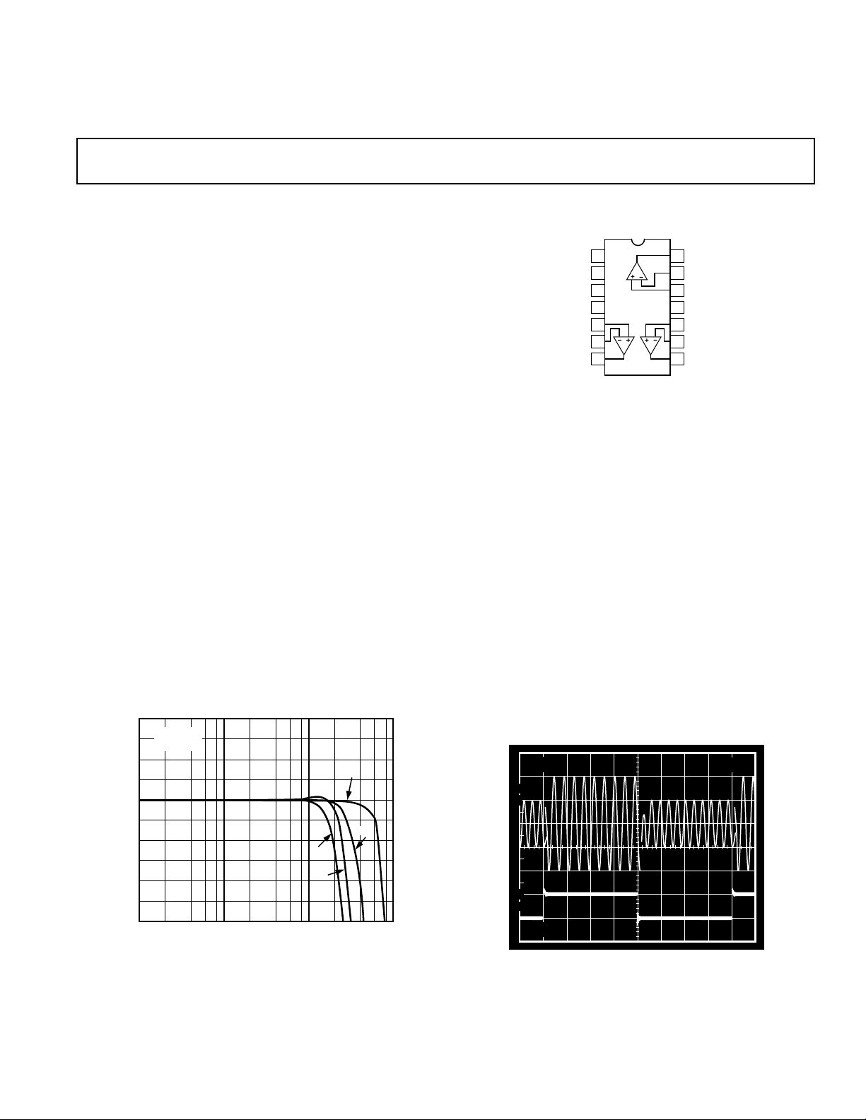
PIN CONFIGURATION
14-Lead DIP and SOIC
OUT2
DISABLE1
DISABLE2
DISABLE3
V
+IN1
–IN1
OUT1
1
2
3
+
4
S
AD813
5
6
7
50 MHz while offering differential gain and phase error of
0.03% and 0.06°. This makes the AD813 ideal for broadcast
and consumer video electronics.
The AD813 offers low power of 5.5 mA per amplifier max and
runs on a single +3 V power supply. The outputs of each amplifier swing to within one volt of either supply rail to easily accommodate video signals. While operating on a single +5 V supply
the AD813 still achieves 0.1 dB flatness to 20 MHz and 0.05%
& 0.05° of differential gain and phase performance. All this is
offered in a small 14-lead plastic DIP or SOIC package. These
features make this triple amplifier ideal for portable and battery
powered applications where size and power are critical.
The outstanding bandwidth of 125 MHz along with 500 V/µs of
slew rate make the AD813 useful in many general purpose, high
speed applications where a single +3 V or dual power supplies
up to ±15 V are needed. Furthermore the AD813 contains a
high speed disable function for each amplifier in order to power
down the amplifier or high impedance the output. This can then
be used in video multiplexing applications. The AD813 is available in the industrial temperature range of –40°C to +85°C in
plastic DIP and SOIC packages as well as chips.
500mV
100
90
10
0%
5V
Figure 2. Channel Switching Characteristics for a 3:1 Mux
One Technology Way, P.O. Box 9106, Norwood, MA 02062-9106, U.S.A.
Tel: 781/329-4700 World Wide Web Site: http://www.analog.com
Fax: 781/326-8703 © Analog Devices, Inc., 1998
14
–IN2
13
+IN2
12
VS–
11
+IN3
10
9
–IN3
8
OUT3
500ns

AD813–SPECIFICATIONS
Dual Supply
(@ TA = +258C, RL = 150 V, unless otherwise noted)
Model AD813A
Conditions V
S
Min Typ Max Units
DYNAMIC PERFORMANCE
–3 dB Bandwidth G = +2, No Peaking ±5 V 45 65 MHz
±15 V 75 100 MHz
Bandwidth for 0.1 dB
Flatness G = +2 ±5 V 15 25 MHz
±15 V 25 50 MHz
Slew Rate
1
G = +2, RL = 1 kΩ±5 V 150 V/µs
±15 V 150 250 V/µs
G = –1, RL = 1 kΩ±5 V 225 V/µs
±15 V 450 V/µs
Settling Time to 0.1% G = –1, R
V
= 3 V Step ±5 V 50 ns
O
= 1 kΩ
L
VO = 10 V Step ±15 V 40 ns
NOISE/HARMONIC PERFORMANCE
Total Harmonic Distortion fC = 1 MHz, RL = 1 kΩ±15 V –90 dBc
Input Voltage Noise f = 10 kHz ±5 V, ±15 V 3.5 nV√Hz
Input Current Noise f = 10 kHz, +In ±5 V, ±15 V 1.5 pA√Hz
–In ±5 V, ±15 V 18 pA√Hz
Differential Gain Error NTSC, G = ±2, R
= 150 Ω±5 V 0.08 %
L
±15 V 0.03 0.09 %
Differential Phase Error ±5 V 0.13 Degrees
±15 V 0.06 0.12 Degrees
DC PERFORMANCE
Input Offset Voltage ±5 V, ±15 V 2 5 mV
T
MIN–TMAX
12 mV
Offset Drift ±5 V, ±15 V 15 µV/°C
–Input Bias Current ±5 V, ±15 V 5 30 µA
T
MIN–TMAX
35 µA
+Input Bias Current ± 5 V, ±15 V 0.5 1.7 µA
Open-Loop Voltage Gain V
Open-Loop Transresistance V
T
MIN–TMAX
= ±2.5 V, RL = 150 Ω±5 V 69 76 dB
O
T
MIN–TMAX
V
= ±10 V, RL = 1 kΩ±15 V 73 82 dB
O
T
MIN–TMAX
= ±2.5 V, RL = 150 Ω±5 V 300 500 kΩ
O
T
MIN–TMAX
= ±10 V, RL = 1 kΩ±15 V 400 900 kΩ
V
O
T
MIN–TMAX
66 dB
72 dB
200 kΩ
300 kΩ
2.5 µA
INPUT CHARACTERISTICS
Input Resistance +Input ±15 V 15 MΩ
–Input ±15 V 65 Ω
Input Capacitance +Input ±15 V 1.7 pF
Input Common Mode ±5 V ±4.0 V
Voltage Range ±15 V ±13.5 V
Common-Mode Rejection Ratio
Input Offset Voltage V
= ±2.5 V ±5 V 54 58 dB
CM
–Input Current 23µA/V
±Input Current 0.07 0.15 µA/V
Input Offset Voltage V
= ±10 V ±15 V 57 62 dB
CM
–Input Current 1.5 3.0 µA/V
+Input Current 0.05 0.1 µA/V
–2–
REV. B

Model AD813A
Conditions V
S
Min Typ Max Units
OUTPUT CHARACTERISTICS
Output Voltage Swing R
= 150 Ω, T
L
= 1 kΩ, T
R
L
MIN–TMAX
MIN–TMAX
±5 V 3.5 3.8 ±V
±15 V 13.6 14.0 ±V
Output Current ±5 V 25 40 mA
±15 V 30 50 mA
Short Circuit Current G = +2, R
= 715 Ω±15 V 100 mA
F
VIN = 2 V
MATCHING CHARACTERISTICS
Dynamic
Crosstalk G = +2, f = 5 MHz ±5 V, ±15 V –65 dB
Gain Flatness Match G = +2, f = 40 MHz ±15 V 0.1 dB
DC
Input Offset Voltage T
–Input Bias Current T
MIN–TMAX
MIN–TMAX
±5 V, ±15 V 0.5 3.5 mV
±5 V, ±15 V 2 25 µA
POWER SUPPLY
Operating Range ±1.2 ±18 V
Quiescent Current Per Amplifier ±5 V 3.5 4.0 mA
±15 V 4.5 5.5 mA
T
MIN–TMAX
±15 V 6.7 mA
Quiescent Current, Powered Down Per Amplifier ±5 V 0.5 0.65 mA
±15 V 0.75 1.0 mA
Power Supply Rejection Ratio
Input Offset Voltage VS = ±1.5 V to ±15 V 72 80 dB
–Input Current 0.3 0.8 µA/V
+Input Current 0.005 0.05 µA/V
AD813
DISABLE CHARACTERISTICS
Off Isolation f = 5 MHz ±5 V, ±15 V –57 dB
Off Output Impedance G = +1 ±5 V, ±15 V 12.5 pF
Channel-to-Channel 2 or 3 Channels ±5 V, ±15 V –65 dB
Isolation Mux, f = 5 MHz
Turn-On Time ±5 V, ±15 V 100 ns
Turn-Off Time 80 ns
NOTES
1
Slew rate measurement is based on 10% to 90% rise time in the specified closed-loop gain.
Specifications subject to change without notice.
REV. B
–3–

AD813–SPECIFICATIONS
Single Supply
(@ TA = +258C, RL = 150 V, unless otherwise noted)
Model AD813A
Conditions V
S
Min Typ Max Units
DYNAMIC PERFORMANCE
–3 dB Bandwidth G = +2, No Peaking +5 V 35 50 MHz
+3 V 25 40 MHz
Bandwidth for 0.1 dB
Flatness G = +2 +5 V 12 20 MHz
+3 V 8 15 MHz
Slew Rate
1
G = +2, RL = 1 kΩ +5 V 100 V/µs
+3 V 50 V/µs
NOISE/HARMONIC PERFORMANCE
Input Voltage Noise f = 10 kHz +5 V, +3 V 3.5 nV√Hz
Input Current Noise f = 10 kHz, +In +5 V, +3 V 1.5 pA√
–In +5 V, +3 V 18 pA√
Differential Gain Error
2
Differential Phase Error
2
NTSC, G = +2, RL = 150 Ω +5 V 0.05 %
G = +1 +3 V 0.2 %
G = +2 +5 V 0.05 Degrees
G = +1 +3 V 0.2 Degrees
DC PERFORMANCE
Input Offset Voltage +5 V, +3 V 1.5 5 mV
T
MIN–TMAX
10 mV
Offset Drift +5 V, +3 V 7 µV/°C
–Input Bias Current +5 V, +3 V 7 30 µA
T
MIN–TMAX
40 µA
+Input Bias Current +5 V, +3 V 0.5 1.7 µA
2.5 µA
Open-Loop Voltage Gain V
Open-Loop Transresistance V
T
MIN–TMAX
= +2.5 V p-p +5 V 65 70 dB
O
= +0.7 V p-p +3 V 69 dB
V
O
= +3 V p-p +5 V 180 300 kΩ
O
VO = +1 V p-p +3 V 225 kΩ
Hz
Hz
INPUT CHARACTERISTICS
Input Resistance +Input +5 V, +3 V 15 MΩ
–Input +5 V 90 Ω
Input Capacitance +Input 2 pF
Input Common Mode +5 V 1.0 4.0 V
Voltage Range +3 V 1.0 2.0 V
Common-Mode Rejection Ratio
Input Offset Voltage V
= 1.25 V to 3.75 V +5 V 54 58 dB
CM
–Input Current 3 6.5 µA/V
+Input Current 0.1 0.2 µA/V
Input Offset Voltage V
= 1 V to 2 V +3 V 56 dB
CM
–Input Current 3.5 µA/V
+Input Current 0.1 µA/V
OUTPUT CHARACTERISTICS
Output Voltage Swing p-p RL = 150 Ω, T
MIN–TMAX
+5 V 3.0 3.2 ± V p-p
+3 V 1.0 1.3 ± V p-p
Output Current +5 V 20 30 mA
+3 V 15 25 mA
Short Circuit Current G = +2, RF = 715 Ω +5 V 40 mA
VIN = 1 V
–4– REV. B
Model AD813A
Conditions V
S
Min Typ Max Units
MATCHING CHARACTERISTICS
Dynamic
Crosstalk G = +2, f = 5 MHz +5 V, +3 V –65 dB
Gain Flatness Match G = +2, f = 20 MHz +5 V, +3 V 0.1 dB
DC
Input Offset Voltage T
–Input Bias Current T
MIN–TMAX
MIN–TMAX
+5 V, +3 V 0.5 3.5 mV
+5 V, +3 V 2 25 µA
POWER SUPPLY
Operating Range 2.4 36 V
Quiescent Current Per Amplifier +5 V 3.2 4.0 mA
+3 V 3.0 4.0 mA
T
MIN–TMAX
+5 V 5.0 mA
Quiescent Current, Powered Down Per Amplifier +5 V 0.4 0.6 mA
+3 V 0.4 0.5 mA
Power Supply Rejection Ratio
Input Offset Voltage V
= +3.0 V to +30 V 76 dB
S
–Input Current 0.3 µA/V
+Input Current 0.005 µA/V
DISABLE CHARACTERISTICS
Off Isolation f = 5 MHz +5 V, +3 V –55 dB
Off Output Impedance G = +1 +5 V, +3 V 13 pF
Channel-to-Channel 2 or 3 Channel +5 V, +3 V –65 dB
Isolation Mux, f = 5 MHz
Turn-On Time +5 V, +3 V 100 ns
Turn-Off Time 80 ns
AD813
TRANSISTOR COUNT 111
NOTES
1
Slew rate measurement is based on 10% to 90% rise time in the specified closed-loop gain.
2
Single supply differential gain and phase are measured with the ac coupled circuit of Figure 52.
Specifications subject to change without notice.
ABSOLUTE MAXIMUM RATINGS
Supply Voltage . . . . . . . . . . . . . . . . . . . . . . . . . . . . . . . . ±18 V
Internal Power Dissipation
2
Plastic (N) . . . . . . . . . . . . . . . . . . . . . . . . . . . . . . 1.6 Watts
Small Outline (R) . . . . . . . . . . . . . . . . . . . . . . . . . 1.0 Watts
Input Voltage (Common Mode) . . . . . . . . . . . . . . . . . . . ±V
Differential Input Voltage . . . . . . . . . . . . . . . . . . . . . . . . ±6V
Output Short Circuit Duration
. . . . . . . . . . . . . . . . . . . . . . . Observe Power Derating Curves
Storage Temperature Range N, R . . . . . . . . –65°C to +125°C
Operating Temperature Range
AD813A . . . . . . . . . . . . . . . . . . . . . . . . . . . –40°C to +85°C
1
Model Range Description Options
AD813AN –40°C to +85°C 14-Lead Plastic DIP N-14
S
AD813AR-14 –40°C to +85°C 14-Lead Plastic SOIC R-14
AD813ACHIPS –40°C to +85°C Die Form
AD813AR-REEL 13" REEL
AD813AR-REEL7 7" REEL
5962-9559601M2A* –55°C to +125°C 20-Lead LCC
*Refer to official DSCC drawing for tested specifications and pin configuration.
ORDERING GUIDE
Temperature Package Package
Lead Temperature Range (Soldering 10 sec) . . . . . . . +300°C
NOTES
1
Stresses above those listed under Absolute Maximum Ratings may cause perma-
nent damage to the device. This is a stress rating only; functional operation of the
device at these or any other conditions above those indicated in the operational
section of this specification is not implied. Exposure to absolute maximum rating
conditions for extended periods may affect device reliability.
2
Specification is for device in free air:
14-Lead Plastic DIP Package: θJA = 75°C/W
14-Lead SOIC Package: θJA = 120°C/W
REV. B
–5–
AD813
WARNING!
ESD SENSITIVE DEVICE
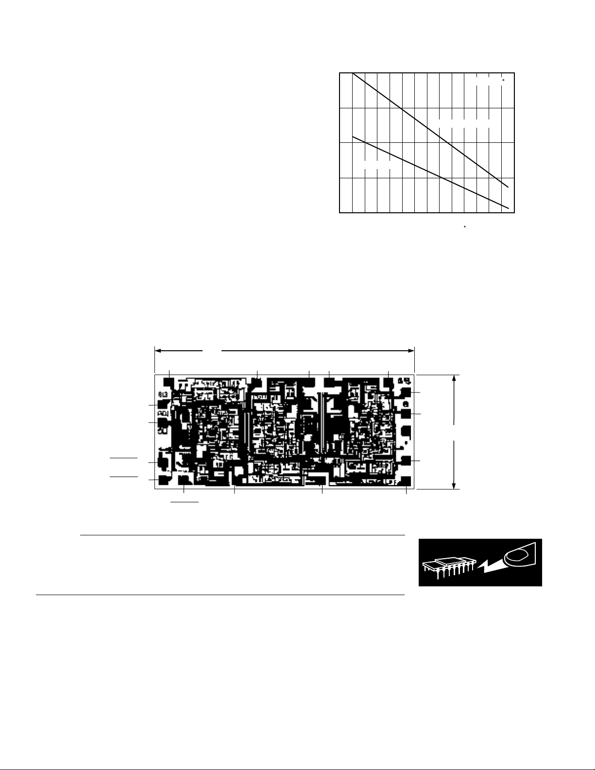
Maximum Power Dissipation
The maximum power that can be safely dissipated by the
AD813 is limited by the associated rise in junction temperature.
The maximum safe junction temperature for the plastic encapsulated parts is determined by the glass transition temperature
of the plastic, about 150°C. Exceeding this limit temporarily
may cause a shift in parametric performance due to a change in
the stresses exerted on the die by the package. Exceeding a
junction temperature of 175°C for an extended period can result
in device failure.
While the AD813 is internally short circuit protected, this may
not be enough to guarantee that the maximum junction temperature (150°C) is not exceeded under all conditions. To
ensure proper operation, it is important to observe the derating
curves.
It must also be noted that in (noninverting) gain configurations
(with low values of gain resistor), a high level of input overdrive
can result in a large input error current, which may result in a
significant power dissipation in the input stage. This power
must be included when computing the junction temperature rise
due to total internal power.
METALIZATION PHOTO
Dimensions shown in inches and (mm).
0.124
+IN2
12
(3.15)
VS–
11
2.5
2.0
14-LEAD DIP PACKAGE
1.5
14-LEAD SOIC
1.0
MAXIMUM POWER DISSIPATION – Watts
0.5
–50 80
–40
AMBIENT TEMPERATURE –
20 30 40 50 60 70 90
010–10–20–30
C
T
= +150 C
J
Figure 3. Maximum Power Dissipation vs. Ambient
Temperature
VS–
11
VS–
11
+IN3
10
–IN2 13
OUT2 14
DISABLE1 1
DISABLE2 2
3
DISABLE3
VS+
4
+IN1
5
–IN1
6
CAUTION
ESD (electrostatic discharge) sensitive device. Electrostatic charges as high as 4000 V readily
accumulate on the human body and test equipment and can discharge without detection.
Although the AD813 features proprietary ESD protection circuitry, permanent damage may
occur on devices subjected to high energy electrostatic discharges. Therefore, proper ESD
precautions are recommended to avoid performance degradation or loss of functionality.
9 –IN3
8 OUT3
7 OUT1
0.057
(1.45)
–6–
REV. B

AD813
13
8
11
9
10
12
16
20
141210
864
SUPPLY VOLTAGE – ±Volts
SUPPLY CURRENT – mA
TA = +25 C
20
15
10
5
COMMON-MODE VOLTAGE RANGE – 6Volts
0
020
5
SUPPLY VOLTAGE – 6Volts
10 15
Figure 4. Input Common-Mode Voltage Range vs.
20
18
16
14
12
SUPPLY CURRENT – mA
10
8
Figure 7. Supply Current vs. Junction Temperature
Supply Voltage
20
15
NO LOAD
VS = 615V
JUNCTION TEMPERATURE –
V
= 65V
S
C
140–40–60 120806040 100200–20
10
RL = 150V
5
OUTPUT VOLTAGE – V p-p
0
020
Figure 5. Output Voltage Swing vs. Supply Voltage
5
SUPPLY VOLTAGE – 6Volts
10 15
Figure 8 Supply Current vs. Supply Voltage at Low
Voltages
30
615V SUPPLY
25
20
15
10
OUTPUT VOLTAGE – V p-p
5
0
10 100 10k1k
LOAD RESISTANCE – V
65V SUPPLY
25
20
15
10
5
0
–5
–10
INPUT BIAS CURRENT – mA
–15
–20
–25
–60 140–40 120100806040200–20
, VS = 65V
–I
B
+IB, VS = 65V, 615V
–IB, VS = 615V
JUNCTION TEMPERATURE – C
REV. B –7–
Figure 9. Input Bias Current vs. Junction TemperatureFigure 6. Output Voltage Swing vs. Load Resistance

AD813
4
2
0
–2
–4
–6
–8
–10
–12
INPUT OFFSET VOLTAGE – mV
–14
–16
JUNCTION TEMPERATURE – C
VS = 615V
VS = 65V
140–40–60 120100806040200–20
Figure 10. Input Offset Voltage vs. Junction
Temperature
160
VS = 615V
140
SINK
120
100
SOURCE
80
SHORT CIRCUIT CURRENT – mA
60
40
JUNCTION TEMPERATURE –
C
140–40–60 120806040 100200–20
Figure 11. Short Circuit Current vs. Junction
Temperature
70
60
50
40
OUTPUT CURRENT – mA
30
20
SUPPLY VOLTAGE – 6Volts
20501510
Figure 13. Linear Output Current vs. Supply Voltage
1k
G = +2
100
10
1
5V
100k 100M10M1M10k
S
15V
S
FREQUENCY – Hz
0.1
CLOSED-LOOP OUTPUT RESISTANCE – V
0.01
Figure 14. Closed-Loop Output Resistance vs.
Frequency
80
70
60
50
V
= 65V
40
OUTPUT CURRENT – mA
30
20
JUNCTION TEMPERATURE –
VS = 615V
S
140–40–60 120806040 100200–20
C
Figure 12. Linear Output Current vs. Junction
Temperature
1M
100k
10k
1k
ΩOUTPUT RESISTANCE – V
100
100k
1M
FREQUENCY – Hz
10M
Figure 15. Output Resistance vs. Frequency, Disabled
State
–8–
100M
REV. B

AD813
100
INVERTING INPUT CURRENT NOISE
10
VOLTAGE NOISE
VOLTAGE NOISE – nV/ Hz
1
10
100 100k10k1k
FREQUENCY – Hz
NONINVERTING INPUT
CURRENT NOISE
Figure 16. Input Current and Voltage Noise vs.
Frequency
90
80
70
60
50
40
30
COMMON-MODE REJECTION – dB
20
10
10k
100k 100M10M1M
V
FREQUENCY – Hz
S
= 3V
681V
V
IN
681V
681V
681V
V
OUT
VS = 615V
100
10
CURRENT NOISE – pA/ Hz
1
Figure 19. Open-Loop Transimpedance vs. Frequency
(Relative to 1
120
100
80
TRANSIMPEDANCE – dB
60
40
10k 100k 100M10M1M
–30
G = +2
VO = 2V p-p
VS = 615V: RL = 1kV
–50
VS = 65V: RL = 150V
–70
–90
3RD HARMONIC
VS = 65V
–110
HARMONIC DISTORTION – dBc
2ND
3RD
–130
1k
GAIN
Ω
)
2ND HARMONIC
VS = 65V
10k 100k 1M 10M 100M
PHASE
VS = 3V
FREQUENCY – Hz
FREQUENCY – Hz
= 615V
V
S
VS = 3V
VS = 615V
VS = 615V
0
–45
–90
–135
PHASE – Degrees
–180
Figure 17. Common-Mode Rejection vs. Frequency
80
70
60
50
40
30
20
POWER SUPPLY REJECTION – dB
10
0
10k
615V
61.5V
100k 100M10M1M
FREQUENCY – Hz
Figure 18. Power Supply Rejection vs. Frequency
REV. B –9–
Figure 20. Harmonic Distortion vs. Frequency
10
8
6
4
2
0
–2
–4
–6
OUTPUT SWING FROM 6V TO 0
–8
–10
1% 0.1% 0.025%
20
SETTLING TIME – ns
GAIN = –1
V
= 615V
S
8040 60
Figure 21. Output Swing and Error vs. Settling Time

AD813
p
1000
VS = 615V
900
R
= 500V
L
800
700
600
500
400
SLEW RATE – V/ms
300
200
100
0
OUTPUT STEP SIZE – V p-
G = +10
G = +2
G = +1
Figure 22. Slew Rate vs. Output Step Size
2V
100
90
50ns
G = –1
700
600
500
400
300
SLEW RATE – V/ms
200
100
101096745 832
0
SUPPLY VOLTAGE – 6Volts
G = +10
G = –1
G = +2
G = +1
15.01.50 13.512.010.59.07.56.04.53.0
Figure 25. Maximum Slew Rate vs. Supply Voltage
500mV 20ns
100
V
IN
V
IN
90
10
0%
V
OUT
2V
Figure 23. Large Signal Pulse Response, Gain = +1,
(R
= 750 Ω, RL = 150 Ω, VS = ±5 V)
F
PHASE
3V
+1
GAIN
0
–1
–2
–3
–4
–5
CLOSED-LOOP GAIN – dB
–6
1 10 1000100
5V
3V
5V
FREQUENCY – MHz
VS = 615V
65V
VS = 615V
65V
+90
0
–90
–180
–270
V
OUT
Figure 26. Small Signal Pulse Response, Gain = +1,
(R
= 750 Ω, RL = 150 Ω, VS = ±5 V)
F
140
120
100
PHASE SHIFT – Degrees
–3dB BANDWIDTH – MHz
10
0%
500mV
= 150V
R
L
= 866V
80
60
40
RF = 750V
RF = 1kV
216141210864
SUPPLY VOLTAGE – 6Volts
R
F
Figure 24. Closed-Loop Gain and Phase vs. Frequency,
G = +1
Figure 27. –3 dB Bandwidth vs. Supply Voltage, G = +1
–10–
REV. B

AD813
g
10
90
100
0%
50mV
20ns
500mV
V
IN
V
OUT
500mV
100
90
10
0%
500mV
50ns
V
IN
V
OUT
Figure 28. Large Signal Pulse Response, Gain = +10,
(R
= 357 Ω, RL = 500 Ω, VS = ±15 V)
F
65V
65V
G = +10
= 150V
R
L
0
–90
–180
–270
PHASE SHIFT – Degrees
PHASE
+1
GAIN
0
–1
–2
–3
–4
–5
–6
CLOSED-LOOP GAIN (NORMALIZED) – dB
1 10 1000100
5V
3V
5V
3V
FREQUENCY – MHz
= 615V
V
S
VS = 615V
Figure 29. Closed-Loop Gain and Phase vs. Frequency,
G = +10, R
= 150
L
Ω
Figure 31. Small Signal Pulse Response, Gain = +10,
= 357 Ω, RL = 150 Ω, VS = ±5 V)
(R
F
PHASE
+1
GAIN
0
–1
–2
–3
–4
–5
–6
CLOSED-LOOP GAIN (NORMALIZED) – dB
1 10 1000100
3V
5V
5V
3V
FREQUENCY – MHz
V
S
= 615V
65V
VS = 615V
65V
G = +10
= 1kV
R
L
0
–90
–180
–270
–360
Figure 32. Closed-Loop Gain and Phase vs. Frequency,
G = +10, R
= 1 k
L
Ω
rees
PHASE SHIFT – De
G = +10
R
= 150V
L
80
70
60
50
40
30
–3dB BANDWIDTH – MHz
20
PEAKING 1dB
RF = 154V
216141210864
SUPPLY VOLTAGE – 6Volts
R
F
R
F
= 357V
= 649V
Figure 30. –3 dB Bandwidth vs. Supply Voltage,
= 150
G = +10, R
REV. B –11–
L
Ω
90
80
70
60
RF = 154V
50
40
–3dB BANDWIDTH – MHz
30
20
216141210864
SUPPLY VOLTAGE – 6Volts
Figure 33. –3 dB Bandwidth vs. Supply Voltage,
G = +10, R
= 1 k
L
Ω
G = +10
= 1kV
R
L
RF = 357V
RF = 649V

AD813
g
g
2V
100
90
10
0%
2V
50ns
Figure 34. Large Signal Pulse Response, Gain = –1,
(RF = 750 Ω, RL = 150 Ω, VS = ±5 V)
PHASE
3V
+1
GAIN
0
–1
–2
–3
–4
CLOSED-LOOP GAIN – dB
–5
–6
1 10 1000100
5V
3V
5V
FREQUENCY – MHz
V
S
65V
VS = 615V
65V
G = –1
R
= 150V
L
0
–90
–180
–270
rees
PHASE SHIFT – De
= 615V
Figure 35. Closed-Loop Gain and Phase vs. Frequency,
G = –1, RL = 150
Ω
500mV
100
90
10
0%
500mV
20ns
Figure 37. Small Signal Pulse Response, Gain = –1,
(RF = 750 Ω, RL = 150 Ω, VS = ±5 V)
65V
VS = 615V
65V
G = –10
= 1kV
R
L
0
–90
–180
–270
PHASE
+1
GAIN
0
–1
–2
–3
–4
–5
CLOSED-LOOP GAIN (NORMALIZED) – dB
–6
1 10 1000100
3V
5V
3V
5V
FREQUENCY – MHz
V
= 615V
S
Figure 38. Closed-Loop Gain and Phase vs. Frequency,
G = –10, RL = 1 k
Ω
rees
PHASE SHIFT – De
G = –1
RL = 150V
110
100
90
80
70
60
–3dB BANDWIDTH – MHz
50
40
PEAKING 1.0dB
RF = 681V
216141210864
PEAKING 0.2dB
RF = 715V
SUPPLY VOLTAGE – 6Volts
Figure 36. –3 dB Bandwidth vs. Supply Voltage, G = –1,
= 150
R
L
Ω
80
70
60
RF = 154V
50
40
30
–3dB BANDWIDTH – MHz
20
216141210864
SUPPLY VOLTAGE – 6Volts
R
R
F
= 357V
F
= 649V
Figure 39. –3 dB Bandwidth vs. Supply Voltage,
= 1 k
G = –10, R
Ω
L
–12–
G = –10
R
= 1kV
L
REV. B

AD813
General Consideration
The AD813 is a wide bandwidth, triple video amplifier that
offers a high level of performance on less than 5.5 mA per amplifier of quiescent supply current. With its fast acting power
down switch, it is designed to offer outstanding functionality
and performance at closed-loop inverting or noninverting gains
of one or greater.
Built on a low cost, complementary bipolar process, and achieving bandwidth in excess of 100 MHz, differential gain and phase
errors of better than 0.1% and 0.1° (into 150 Ω), and output
current greater than 40 mA, the AD813 is an exceptionally
efficient video amplifier. Using a conventional current feedback
architecture, its high performance is achieved through careful
attention to design details.
Choice of Feedback & Gain Resistors
Because it is a current feedback amplifier, the closed-loop bandwidth of the AD813 depends on the value of the feedback resistor. The bandwidth also depends on the supply voltage. In
addition, attenuation of the open-loop response when driving
load resistors less than about 250 Ω will also affect the bandwidth. Table I contains data showing typical bandwidths at
different supply voltages for some useful closed-loop gains when
driving a load of 150 Ω. (Bandwidths will be about 20% greater
for load resistances above a few hundred ohms.)
Table I. –3 dB Bandwidth vs. Closed-Loop Gain and
Feedback Resistor , (R
= 150 V)
L
VS (V) Gain RF (V) BW (MHz)
±15 +1 866 125
+2 681 100
+10 357 60
–1 681 100
–10 357 55
±5 +1 750 75
+2 649 65
+10 154 40
–1 649 70
–10 154 40
+5 +1 715 60
+2 619 50
+10 154 30
–1 619 50
–10 154 30
+3 +1 681 50
+2 619 40
+10 154 25
–1 619 40
–10 154 20
To estimate the –3 dB bandwidth for closed-loop gains or feedback resistors not listed in the above table, the following two
pole model for the AD813 may be used:
A
=
CL
RGrC
+
()
FINT
2
S
2
π
G
S R Gr C
++ +
()
FINT
f
2
1
where: ACL= closed-loop gain from “transcapacitance”
G = 1 + R
F/RG
rIN= input resistance of the inverting input
C
= “transcapacitance,” which forms the
T
open-loop dominant pole with the
transresistance
R
= feedback resistor
F
R
= gain resistor
G
f
= frequency of second (nondominant) pole
2
s =2 πj f
Appropriate values for the model parameters at different supply
voltages are listed in Table II. Reasonable approximations for
these values at supply voltages not found in the table can be
obtained by a simple linear interpolation between those tabulated values which ‘bracket’ the desired condition.
Table II. Two Pole Model Parameters at Various Supplies
VS (V) rIN (V)C
(pF) f2 (MHz)
T
±15 85 2.5 150
±5 90 3.8 125
+5 105 4.8 105
+3 115 5.5 95
As discussed in many amplifier and electronics textbooks (such
as Roberge’s Operational Amplifiers: Theory and Practice), the
–3 dB bandwidth for the 2-pole model can be obtained as:
1/2
f
2
+GrIN) C
F
1/2
1/2
T
1/2
T
f
= fn1 − 2d2+(2 − 4d2+ 4d4)
3
where:
and:
[]
f
=
n
d =
(RF+GrIN) C
1
f2(R
[]
2
This model will predict –3 dB bandwidth within about 10% to
15% of the correct value when the load is 150 Ω. However, it is
not accurate enough to predict either the phase behavior or the
frequency response peaking of the AD813.
The choice of feedback resistor is not critical unless it is important to maintain the widest, flattest frequency response. The
resistors recommended in the table are those (metal film values)
that will result in the widest 0.1 dB bandwidth. In those applications where the best control of the bandwidth is desired, 1%
metal film resistors are adequate. Wider bandwidths can be
attained by reducing the magnitude of the feedback resistor (at
the expense of increased peaking), while peaking can be reduced
by increasing the magnitude of the feedback resistor.
REV. B –13–
AD813
Printed Circuit Board Layout Guidelines
As with all wideband amplifiers, printed circuit board parasitics
can affect the overall closed-loop performance. Most important
for controlling the 0.1 dB bandwidth are stray capacitances at
the output and inverting input nodes. Increasing the space between signal lines and ground plane will minimize the coupling.
Also, signal lines connecting the feedback and gain resistors
should be kept short enough that their associated inductance
does not cause high frequency gain errors.
Power Supply Bypassing
Adequate power supply bypassing can be very important when
optimizing the performance of high speed circuits. Inductance
in the supply leads can (for example) contribute to resonant
circuits that produce peaking in the amplifier’s response. In
addition, if large current transients must be delivered to a load,
then large (greater than 1 µF) bypass capacitors are required to
produce the best settling time and lowest distortion. Although
0.1 µF capacitors may be adequate in some applications, more
elaborate bypassing is required in other cases.
When multiple bypass capacitors are connected in parallel, it is
important to be sure that the capacitors themselves do not form
resonant circuits. A small (say 5 Ω) resistor may be required in
series with one of the capacitors to minimize this possibility.
As discussed below, power supply bypassing can have a significant impact on crosstalk performance.
Achieving Low Crosstalk
Measured crosstalk from the output of Amplifier 2 to the input
of Amplifier 1 of the AD813 is shown in Figure 40. All other
crosstalk combinations, (from the output of one amplifier to the
input of another), are a few dB better than this due to the additional distance between critical signal nodes.
–10
–20
–30
–40
–50
–60
–70
CROSSTALK – dB
–80
–90
–100
–110
100k
1M 100M10M
FREQUENCY – Hz
RL = 150V
Figure 40. Worst Case Crosstalk vs. Frequency
A carefully laid-out PC board should be able to achieve the level
of crosstalk shown in the figure. The most significant contributors to difficulty in achieving low crosstalk are inadequate power
supply bypassing, overlapped input and/or output signal paths,
and capacitive coupling between critical nodes.
The bypass capacitors must be connected to the ground plane at
a point close to and between the ground reference points for the
loads. (The bypass of the negative power supply is particularly
important in this regard.) This requires careful planning as
there are three amplifiers in the package, and low impedance
signal return paths must be provided for each load. (Using a
parallel combination of 1 µF, 0.1 µF, and 0.01 µF bypass ca-
pacitors will help to achieve optimal crosstalk.)
The input and output signal return paths (to the bypass caps)
must also be kept from overlapping. Since ground connections
are not of perfectly zero impedance, current in one ground
return path can produce a voltage drop in another ground return path if they are allowed to overlap.
Electric field coupling external to (and across) the package can
be reduced by arranging for a narrow strip of ground plane to be
run between the pins (parallel to the pin rows). Doing this on
both sides of the board can reduce the high frequency crosstalk
by about 5 dB or 6 dB.
Driving Capacitive Loads
When used with the appropriate output series resistor, any load
capacitance can be driven without peaking or oscillation. In
most cases, less than 50 Ω is all that is needed to achieve an
extremely flat frequency response. As illustrated in Figure 44,
the AD813 can be very attractive for driving large capacitive
loads. In this case, the AD813’s high output short circuit current allows for a 150 V/µs slew rate when driving a 510 pF
capacitor.
R
F
0.1mF
+V
S
1.0mF
R
G
V
IN
R
T
4
AD813
11
–V
R
S
C
1.0mF
0.1mF
S
L
V
O
R
L
Figure 41. Circuit for Driving a Capacitive Load
–14–
REV. B

AD813
VS = 65V
G = +2
RF = 750V
RL = 1kV
CL = 10pF
9
6
3
0
–3
CLOSED-LOOP GAIN – dB
1
RS = 30V
10 1000100
FREQUENCY – MHz
RS = 0
RS = 50V
Figure 42. Response to a Small Load Capacitor at
= ±5 V
V
S
VS = 615V
G = +2
RF = 750V
RL = 1kV
9
6
3
0
–3
CLOSED-LOOP GAIN – dB
1
= 510pF, RS = 15V
C
L
10 1000100
FREQUENCY – MHz
CL = 150pF, RS = 30V
Figure 43. Response to a Large Load Capacitor at
V
= ±15 V
S
Overload Recovery
There are three important overload conditions to consider.
They are due to: input common-mode voltage overdrive, output voltage overdrive, and input current overdrive. When the
amplifier is configured for low closed-loop gains, and the input
common-mode voltage range is exceeded, the recovery time will
be very fast, typically under 30 ns. When configured for a
higher gain, and overloaded at the output, the recovery time will
also be short. For example, in a gain of +10, with 6 dB of
input overdrive, the recovery time of the AD813 is about 25 ns
(see Figure 45).
1V
100
90
10
0%
2V
50ns
Figure 45. 6 dB Overload Recovery, G = +10,
= 500 Ω, RF = 357 Ω, VS = ±5 V)
(R
L
In the case of high gains with very high levels of input overdrive,
a longer recovery time will occur. For example, if the input
common-mode voltage range is exceeded in the gain of +10, the
recovery time will be on the order of 100 ns. This is primarily
due to current overloading of the input stage.
As noted in the warning under Maximum Power Dissipation, a
high level of input overdrive in a high noninverting gain circuit
can result in a large current flow in the input stage. Though this
current is internally limited to about 40 mA, its effect on the
total power dissipation may be significant.
100
5V
100
90
10
0%
5V
100ns
Figure 44. Circuit of Figure 38 Driving a 510 pF Load
Capacitor, V
=15 Ω)
R
S
= ±15 V (RL = 1 kΩ, RF = RG = 750 Ω,
S
REV. B –15–

AD813
High Performance Video Line Driver
At a gain of +2, the AD813 makes an excellent driver for a back
terminated 75 Ω video line. Low differential gain and phase
errors and wide 0.1 dB bandwidth can be realized over a wide
range of power supply voltage. Excellent gain and group delay
matching are also attainable over the full operating supply voltage range.
R
G
75V
CABLE
V
IN
75V
+V
4
AD813
11
–V
R
F
S
0.1mF
75V
CABLE
75V
0.1mF
S
75V
V
OUT
Figure 46. A Video Line Driver Operating at a Gain of
= RG from Table I)
+2 (R
F
PHASE
3V
+1
GAIN
0
–1
–2
–3
–4
–5
CLOSED-LOOP GAIN (NORMALIZED) – dB
–6
1
5V
5V
3V
10 1000100
FREQUENCY – MHz
G = +2
R
VS = 615V
VS = 615V
65V
= 150V
L
65V
+90
0
–90
–180
–270
PHASE SHIFT – Degrees
Figure 47. Closed-Loop Gain & Phase vs. Frequency for
the Line Driver
Figures 50 and 51 show the worst case matching; the match
between amplifiers 2 and 3 is typically much better than this.
G = +2
= 150V
R
L
0.2
0.1
0
–0.1
–0.2
–0.3
NORMALIZED GAIN – dB
–0.4
–0.5
100k
1M 100M10M
FREQUENCY – Hz
615V
65V
3V
5V
Figure 49. Fine-Scale Gain (Normalized) vs. Frequency
2.5
2.0
1.5
1.0
0.5
0
–0.5
–1.0
GAIN MATCHING – dB
–1.5
–2.0
–2.5
1 10 1000100
VS = 3V
FREQUENCY – MHz
VS = 615V
G = +2
R
= 150V
L
Figure 50. Closed-Loop Gain Matching vs. Frequency
120
110
100
90
80
70
60
50
–3dB BANDWIDTH – MHz
40
30
20
216141210864
NO PEAKING
SUPPLY VOLTAGE – Volts
RF = 590V
RF = 681V
RF = 750V
20180
Figure 48. –3 dB Bandwidth vs. Supply Voltage for
Gain = +2, R
= 150
L
Ω
10
8
6
4
2
1.0
GROUP DELAY – ns
0.5
0
–0.5
–1.0
100k 1M 100M10M
VS = 3V
DELAY
DELAY MATCHING
FREQUENCY – Hz
5V
65V
615V
VS = 615V
Figure 51. Group Delay and Group Delay Matching vs.
Frequency, G = +2, RL = 150
Ω
–16–
3V
REV. B

AD813
75V
75V
75V
75V
V
OUT
75V
CABLE
1
VIN1
84V
+5V
464V 590V
7
4
5
6
SELECT1
2
VIN2
84V
464V 590V
14
12
13
SELECT2
VIN3
84V
3
464V 590V
8
10
9
SELECT3
11
–5V
Operation Using a Single Supply
The AD813 will operate with total supply voltages from 36 V
down to 2.4 V. With proper biasing (see Figure 52) it can
make an outstanding single supply video amplifier. Since the
input and output voltage ranges extend to within 1 V of the
supply rails, it will handle a 1.3 V peak-to-peak signal on a
single 3.3 V supply, or a 3 V peak-to-peak signal on a single
5 V supply. The small signal 0.1 dB bandwidths will exceed
10 MHz in either case, and the large signal bandwidths will
exceed 6 MHz.
The capacitively coupled cable driver in Figure 52 will achieve
outstanding differential gain and phase errors of 0.05% and 0.05
degrees respectively on a single 5 V supply. Resistor R2, in this
circuit, is selected to optimize the differential gain and phase by
biasing the amplifier in its most linear region.
619V 619V
C3
30mF
C2
1mF
9kV
C1
2mF
V
IN
12.4kV
R3
1kV
R1
R2
AD813
11
+5V
C
4
OUT
47mF
75V
75V
CABLE
75V
V
OUT
Figure 52. Biasing for Single Supply Operation
VS = 5V
G = +2
= 619V
0.5
0
–0.5
–1.0
–1.5
–2.0
CLOSED-LOOP GAIN – dB
–2.5
–3.0
–3.5
1
10 1000100
Figure 53. Closed-Loop Gain and Phase vs. Frequency,
PHASE
GAIN
FREQUENCY – MHz
R
F
R
L
= 150V
0
–90
–180
–270
Circuit of Figure 52
1V
50ns
Disable Mode Operation
Pulling the voltage on any one of the Disable pins about 2.5 V
down from the positive supply will put the corresponding amplifier into a disabled, powered down, state. In this condition, the
amplifier’s quiescent supply current drops to about 0.5 mA, its
output becomes a high impedance, and there is a high level of
isolation from input to output. In the case of the gain of two
line driver for example, the impedance at the output node will
be about the same as for a 1.4 kΩ resistor (the feedback plus
gain resistors) in parallel with a 12.5 pF capacitor and the input
to output isolation will be about 65 dB at 1 MHz.
Leaving the Disable pin disconnected (floating) will leave the
corresponding amplifier operational, in the enabled state. The
input impedance of the disable pins is about 35 kΩ in parallel
with a few pF. When grounded, about 50 µA flows out of a
disable pin on ±5 V supplies.
Input voltages greater than about 1.5 V peak-to-peak will defeat
the isolation. In addition, large signals (greater than 3 V peakto-peak) applied to the output node will cause the output impedance to drop significantly.
When the Disable pins are driven by complementary output
CMOS logic (such as the 74HC04), the disable time is about
80 ns (until the output goes high impedance) and the enable
time is about 100 ns (to low impedance output) on ± 15 V supplies. When operated on ±15 V supplies, the disable pins
should be driven by open drain logic. In this case, pull-up resistors from the disable pins to the plus supply will ensure minimum switching time.
PHASE SHIFT – Degrees
100
90
10
Figure 54. Pulse Response for the Circuit of Figure 52
with +V
REV. B –17–
0%
= 5 V
S
500mV
500mV
V
IN
V
OUT
Figure 55. A Fast Switching 3:1 Video Mux
(Supply Bypassing Not Shown)

AD813
10
90
100
0%
1V
1V
50ns
V
IN
V
OUT
+
– V
OUT
–
3:1 Video Multiplexer
Wiring the amplifier outputs together will form a 3:1 mux with
outstanding gain flatness. Figure 55 shows a recommended
configuration which results in –0.1 dB bandwidth of 20 MHz
and OFF channel isolation of 60 dB at 10 MHz on ± 5 V supplies. The time to switch between channels is about 180 ns.
Switching time is only slightly affected by signal level.
500mV
100
90
10
0%
5V
500ns
Figure 56. Channel Switching Characteristic for the
3:1 Mux
–10
–20
–30
–40
–50
–60
–70
FEEDTHROUGH – dB
–80
–90
–100
–110
100k
1M 100M10M
FREQUENCY – Hz
Figure 57. 3:1 Mux OFF Channel Feedthrough vs.
Frequency
Single Supply Differential Line Driver
Due to its outstanding overall performance on low supply voltages, the AD813 makes possible exceptional differential transmission on very low power. The circuit of Figure 59 will convert
a single-ended, ground referenced signal to a differential signal
whose common-mode reference is set to one half the supply
voltage. This allows for a greater than 2 V peak-to-peak signal
swing on a single 3 V power supply. A bandwidth over 30 MHz
is achieved with 20 mA of output drive on only 30 mW of quiescent power (excluding load current).
715V 715V
1mF
+3V
4
2
1mF
V
IN
715V 715V
715V 715V
1mF
3
11
715V 715V
V
+
OUT
R
L1
+3V
715V
1kV
1mF
1
V
–
OUT
R
L2
9kV
10kV
Figure 59. Single 3 V Supply Differential Line Driver
with 2 V Swing
PHASE
0.5
0
–0.5
–1.0
–1.5
–2.0
–2.5
CLOSED-LOOP GAIN – dB
–3.0
GAIN
1 10 100
FREQUENCY – MHz
0
–45
–90
–135
–180
PHASE SHIFT – Degrees
Figure 60. Differential Driver Pulse Response (VS = 3 V,
R
= RL2 = 200 Ω)
L1
Figure 58. 3:1 Mux ON Channel Gain and Phase vs.
Frequency
–18–
REV. B

OUTLINE DIMENSIONS
14
17
8
0.795 (20.19)
0.725 (18.42)
0.280 (7.11)
0.240 (6.10)
PIN 1
0.325 (8.25)
0.300 (7.62)
0.015 (0.381)
0.008 (0.204)
0.195 (4.95)
0.115 (2.93)
SEATING
PLANE
0.022 (0.558)
0.014 (0.356)
0.060 (1.52)
0.015 (0.38)
0.210 (5.33)
MAX
0.130
(3.30)
MIN
0.070 (1.77)
0.045 (1.15)
0.100
(2.54)
BSC
0.160 (4.06)
0.115 (2.93)
Dimensions shown in inches and (mm).
14-Lead Plastic DIP
(N-14)
14-Lead SOIC
(R-14)
0.3444 (8.75)
0.3367 (8.55)
AD813
C1860b–0–5/98
0.1574 (4.00)
0.1497 (3.80)
0.0098 (0.25)
0.0040 (0.10)
SEATING
PLANE
14 8
PIN 1
0.0500
0.0192 (0.49)
(1.27)
0.0138 (0.35)
BSC
0.2440 (6.20)
71
0.2284 (5.80)
0.0688 (1.75)
0.0532 (1.35)
0.0099 (0.25)
0.0075 (0.19)
0.0196 (0.50)
0.0099 (0.25)
8
0
0.0500 (1.27)
0.0160 (0.41)
x 45
REV. B –19–
PRINTED IN U.S.A.
 Loading...