

Low Distortion
1
2
3
4
8
7
6
5
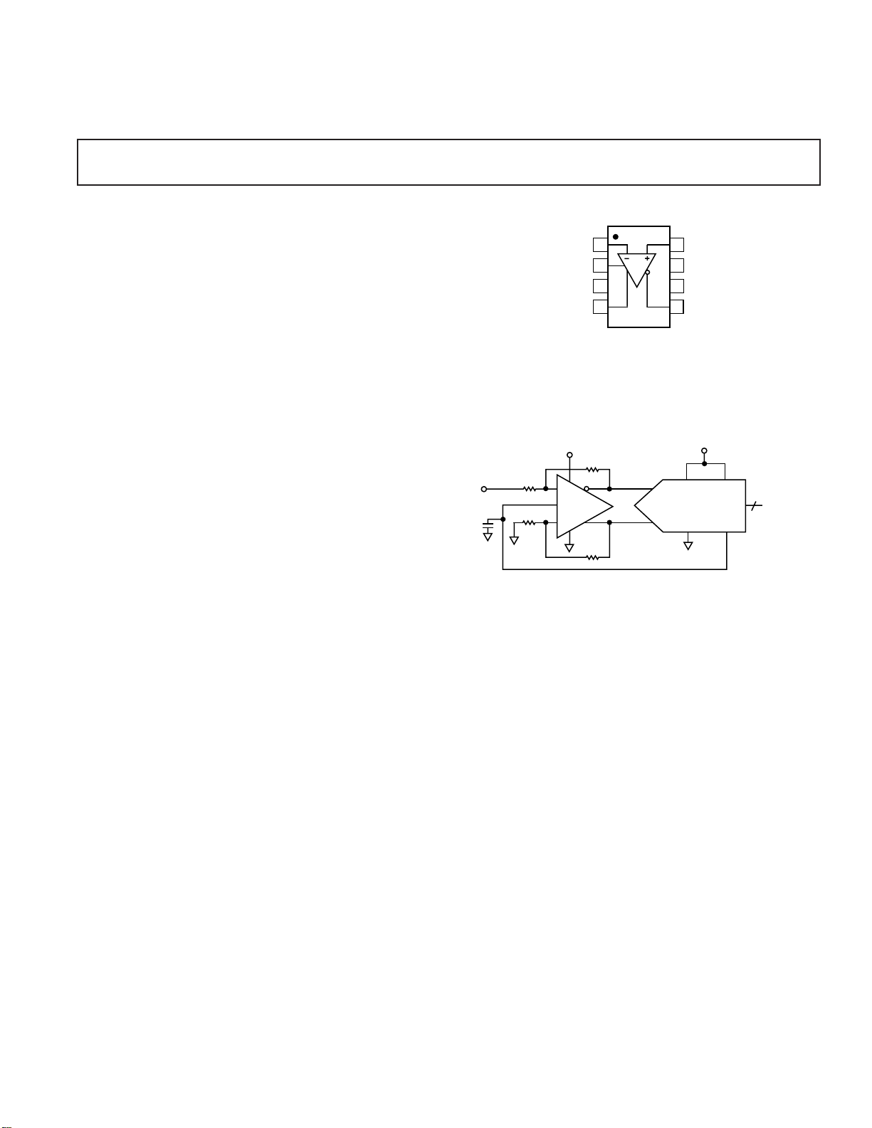
AD8138
NC
V
OCM
–OUT
V+
NC = NO CONNECT
+IN
V–
–IN
+OUT
a
FEATURES
Easy to Use Single-Ended-to-Differential Conversion
Adjustable Output Common-Mode Voltage
Externally Adjustable Gain
Low Harmonic Distortion
–94 dBc—Second, <–114 dBc—Third @ 5 MHz into
800 ⍀ Load
–87 dBc—Second, –85 dBc—Third @ 20 MHz into
800 ⍀ Load
–3 dB Bandwidth of 320 MHz, G = +1
Fast Settling to 0.01% of 16 ns
Slew Rate 1150 V/s
Fast Overdrive Recovery of 4 ns
Low Input Voltage Noise of 5 nV/√Hz
1 mV Typical Offset Voltage
Wide Supply Range +3 V to ⴞ5 V
Low Power 90 mW on +5 V
0.1 dB Gain Flatness to 40 MHz
Available in 8-Lead SOIC
APPLICATIONS
ADC Driver
Single-Ended-to-Differential Converter
IF and Baseband Gain Block
Differential Buffer
Line Driver
Differential ADC Driver
AD8138
FUNCTIONAL BLOCK DIAGRAM
TYPICAL APPLICATION CIRCUIT
AVDD DVDD
AIN
AIN
AVSS
+5V
ADC
DIGITAL
V
REF
OUTPUTS
+5V
499V
V
IN
499V
V
499V
OCM
+
AD8138
–
499V
PRODUCT DESCRIPTION
AD8138 is a major advancement over op amps for differential
signal processing. The AD8138 can be used as a single-endedto-differential amplifier or as a differential-to-differential amplifier. The AD8138 is as easy to use as an op amp, and greatly
simplifies differential signal amplification and driving.
Manufactured on ADI’s proprietary XFCB bipolar process, the
AD8138 has a –3 dB bandwidth of 320 MHz and delivers a
differential signal with the lowest harmonic distortion available
in a differential amplifier. The AD8138 has a unique internal
feedback feature that provides output gain and phase matching
that are balanced, suppressing even order harmonics. The internal feedback circuit also minimizes any gain error that would be
associated with the mismatches in the external gain setting
resistors.
The AD8138’s differential output helps balance the input-todifferential ADCs, maximizing the performance of the ADC.
The AD8138 eliminates the need for a transformer with high
REV. A
Information furnished by Analog Devices is believed to be accurate and
reliable. However, no responsibility is assumed by Analog Devices for its
use, nor for any infringements of patents or other rights of third parties
which may result from its use. No license is granted by implication or
otherwise under any patent or patent rights of Analog Devices.
performance ADCs, preserving the low frequency and dc information. The common-mode level of the differential output is
adjustable by a voltage on the V
pin, easily level-shifting
OCM
the input signals for driving single supply ADCs. Fast overload
recovery preserves sampling accuracy.
The AD8138 distortion performance makes it an ideal ADC
driver for communication systems, with distortion performance
good enough to drive state-of-the-art 10- to 16-bit converters
at high frequencies. The AD8138’s high bandwidth and IP3
also make it appropriate for use as a gain block in IF and
baseband signal chains. The AD8138 offset and dynamic performance make it well suited for a wide variety of signal processing and data acquisition applications.
The AD8138 is offered in an 8-lead SOIC that operates over
the industrial temperature range of –40°C to +85°C.
One Technology Way, P.O. Box 9106, Norwood, MA 02062-9106, U.S.A.
Tel: 781/329-4700 World Wide Web Site: http://www.analog.com
Fax: 781/326-8703 © Analog Devices, Inc., 1999

AD8138–SPECIFICATIONS
(@ +25ⴗC, VS = ⴞ5 V, V
= 0, G = +1, R
OCM
= 500 ⍀, unless otherwise noted.
L,dm
Refer to Figure 1 for test setup and label descriptions. All specifications refer to single-ended input and differential outputs unless noted.)
AD8138
Parameter Conditions Min Typ Max Units
ⴞDIN to ⴞOUT Specifications
DYNAMIC PERFORMANCE
–3 dB Small Signal Bandwidth V
Bandwidth for 0.1 dB Flatness V
Large Signal Bandwidth V
Slew Rate V
Settling Time 0.01%, V
Overdrive Recovery Time VIN = 5 V to 0 V Step, G = +2 4 ns
NOISE/HARMONIC PERFORMANCE
Second Harmonic V
Third Harmonic V
IMD 20 MHz –77 dBc
IP3 20 MHz 37 dBm
Voltage Noise (RTI) f = 100 kHz to 40 MHz 5 nV/√Hz
Input Current Noise f = 100 kHz to 40 MHz 2 pA/√Hz
INPUT CHARACTERISTICS
Offset Voltage V
Input Bias Current 3.5 7 µA
Input Resistance Differential 6 MΩ
Input Capacitance 1pF
Input Common-Mode Voltage –4.7 – +3.4 V
CMRR ∆V
OUTPUT CHARACTERISTICS
Output Voltage Swing Maximum ∆V
Output Current 95 mA
Output Balance Error ∆V
V
to ⴞOUT Specifications
OCM
DYNAMIC PERFORMANCE
–3 dB Bandwidth 250 MHz
Slew Rate 330 V/µs
DC PERFORMANCE
Input Voltage Range ±3.8 V
Input Resistance 200 kΩ
Input Offset Voltage V
Input Bias Current 0.5 µA
V
CMRR [∆V
OCM
Gain ∆V
POWER SUPPLY
Operating Range ±1.4 ±5.5 V
Quiescent Current 18 20 23 mA
Power Supply Rejection Ratio ∆V
OPERATING TEMPERATURE RANGE –40 +85 °C
NOTES
Harmonic Distortion Performance is equal or slightly worse with higher values of R
Specifications subject to change without notice.
= 0.5 V p-p, CF = 0 pF 290 320 MHz
OUT
V
= 0.5 V p-p, CF = 1 pF 225 MHz
OUT
= 0.5 V p-p, CF = 0 pF 30 MHz
OUT
= 2 V p-p, CF = 0 pF 265 MHz
OUT
= 2 V p-p, C
OUT
OUT
= 2 V p-p, 5 MHz, R
OUT
V
= 2 V p-p, 20 MHz, R
OUT
V
= 2 V p-p, 70 MHz, R
OUT
= 2 V p-p, 5 MHz, R
OUT
V
= 2 V p-p, 20 MHz, R
OUT
V
= 2 V p-p, 70 MHz, R
OUT
= V
OS,dm
T
MIN–TMAX
T
MIN–TMAX
OUT,dm
= 0 pF 1150 V/µs
F
= 2 V p-p, CF = 1 pF 16 ns
= 800 Ω –94 dBc
L,dm
= 800 Ω –87 dBc
L,dm
= 800 Ω –62 dBc
L,dm
= 800 Ω –114 dBc
L,dm
= 800 Ω –85 dBc
L,dm
= 800 Ω –57 dBc
L,dm
/2; V
DIN+
= V
DIN–
= V
= 0 V –2.5 ±1 2.5 mV
OCM
Variation ±4 µV/°C
Variation –0.01 µA/°C
Common Mode 3 MΩ
/∆V
T
OUT,dm
/∆V
OUT,cm
= V
OS,cm
OUT,dm
/∆V
OUT,cm
to T
MIN
/∆VS; ∆VS = ±1 V –90 –70 dB
OUT,dm
; ∆V
IN,cm
; Single-Ended Output 7.75 V p-p
OUT
OUT,dm
; V
OUT,cm
/∆V
]; ∆V
OCM
OCM; ∆VOCM
Variation 40 µA/°C
MAX
= ±1 V –75 –70 dB
IN,cm
; ∆V
DIN+
= 1 V –66 dB
OUT,dm
= V
OCM
DIN–
= V
= 0 V –3.5 ±1 3.5 mV
OCM
= ±1 V –75 dB
= ±1 V 0.9955 1 1.0045 V/V
. See Figures 14 and 15 for more information.
L,dm
–2–
REV. A

AD8138
SPECIFICATIONS
(@ +25ⴗC, VS = +5 V, V
for test setup and label descriptions. All specifications refer to single-ended input and differential outputs unless noted.)
Parameter Conditions Min Typ Max Units
ⴞDIN to ⴞOUT Specifications
DYNAMIC PERFORMANCE
–3 dB Small Signal Bandwidth V
Bandwidth for 0.1 dB Flatness V
Large Signal Bandwidth V
Slew Rate V
Settling Time 0.01%, V
Overdrive Recovery Time VIN = 2.5 V to 0 V Step, G = +2 4 ns
NOISE/HARMONIC PERFORMANCE
Second Harmonic V
Third Harmonic V
IMD 20 MHz –74 dBc
IP3 20 MHz 35 dBm
Voltage Noise (RTI) f = 100 kHz to 40 MHz 5 nV/√Hz
Input Current Noise f = 100 kHz to 40 MHz 2 pA/√Hz
INPUT CHARACTERISTICS
Offset Voltage V
Input Bias Current 3.5 7 µA
Input Resistance Differential 6 MΩ
Input Capacitance 1pF
Input Common-Mode Voltage –0.3 – +3.2 V
CMRR ∆V
OUTPUT CHARACTERISTICS
Output Voltage Swing Maximum ∆V
Output Current 95 mA
Output Balance Error ∆V
V
to ⴞOUT Specifications
OCM
DYNAMIC PERFORMANCE
–3 dB Bandwidth 220 MHz
Slew Rate 250 V/µs
DC PERFORMANCE
Input Voltage Range +1.0 – +3.8 V
Input Resistance 100 kΩ
Input Offset Voltage V
Input Bias Current 0.5 µA
V
CMRR [∆V
OCM
Gain ∆V
POWER SUPPLY
Operating Range 2.7 11 V
Quiescent Current 15 20 21 mA
Power Supply Rejection Ratio ∆V
OPERATING TEMPERATURE RANGE –40 +85 °C
NOTES
Harmonic Distortion Performance is equal or slightly worse with higher values of R
Specifications subject to change without notice.
= 0.5 V p-p, CF = 0 pF 280 310 MHz
OUT
V
= 0.5 V p-p, CF = 1 pF 225 MHz
OUT
= 0.5 V p-p, CF = 0 pF 29 MHz
OUT
= 2 V p-p, CF = 0 pF 265 MHz
OUT
= 2 V p-p, C
OUT
= 2 V p-p, 5 MHz, R
OUT
V
= 2 V p-p, 20 MHz, R
OUT
V
= 2 V p-p, 70 MHz, R
OUT
= 2 V p-p, 5 MHz, R
OUT
V
= 2 V p-p, 20 MHz, R
OUT
V
= 2 V p-p, 70 MHz, R
OUT
= V
OS,dm
T
MIN–TMAX
T
MIN–TMAX
Common Mode 3 MΩ
OUT,dm
OUT,cm
= V
OS,cm
OUT,dm
OUT,cm
T
to T
MIN
OUT,dm
= +2.5 V, G = +1, R
OCM
= 500 ⍀, unless otherwise noted. Refer to Figure 1
L,dm
AD8138
= 0 pF 950 V/µs
F
= 2 V p-p, CF = 1 pF 16 ns
OUT
= 800 Ω –90 dBc
L,dm
= 800 Ω –79 dBc
L,dm
= 800 Ω –60 dBc
L,dm
= 800 Ω –100 dBc
L,dm
= 800 Ω –82 dBc
L,dm
= 800 Ω –53 dBc
L,dm
OUT,dm
/2; V
DIN+
= V
DIN–
= V
= 2.5 V –2.5 ±12.5mV
OCM
Variation ±4 µV/°C
Variation –0.01 µA/°C
/∆V
; ∆V
IN,cm
OUT
/∆V
OUT,dm
; V
OUT,cm
/∆V
OCM
/∆V
OCM; ∆VOCM
Variation 40 µA/°C
MAX
= 1 V –75 –70 dB
IN,cm
; Single-Ended Output 2.9 V p-p
; ∆V
DIN+
]; ∆V
= 1 V –65 dB
OUT,dm
= V
OCM
DIN–
= V
= 2.5 V –5 ±15mV
OCM
= 2.5 ± 1 V –70 dB
= 2.5 ± 1 V 0.9968 1 1.0032 V/V
/∆VS; ∆VS = ±1 V –90 –70 dB
. See Figures 14 and 15 for more information.
L,dm
–3–REV. A
AD8138
1
2
3
4
8
7
6
5
AD8138
NC
V
OCM
–OUT
V+
NC = NO CONNECT
+IN
V–
–IN
+OUT
ABSOLUTE MAXIMUM RATINGS
1
Supply Voltage . . . . . . . . . . . . . . . . . . . . . . . . . . . . . . . ±5.5 V
V
. . . . . . . . . . . . . . . . . . . . . . . . . . . . . . . . . . . . . . . . ±V
OCM
Internal Power Dissipation . . . . . . . . . . . . . . . . . . . . 550 mW
2
θ
. . . . . . . . . . . . . . . . . . . . . . . . . . . . . . . . . . . . . 155°C/W
JA
S
Operating Temperature Range . . . . . . . . . . . –40°C to +85°C
Storage Temperature Range . . . . . . . . . . . . –65°C to +150°C
Lead Temperature (Soldering 10 sec) . . . . . . . . . . . . +300°C
NOTES
1
Stresses above those listed under Absolute Maximum Ratings may cause permanent damage to the device. This is a stress rating only, functional operation of the
device at these or any other conditions above listed in the operational section of this
specification is not implied. Exposure to Absolute Maximum Ratings for any
extended periods may affect device reliability.
2
Thermal resistance measured on SEMI standard 4-layer board.
R
= 499V
F
RG = 499V
49.9V
R
G
24.9V
= 499V
AD8138
RF = 499V
R
= 499V
L,dm
Figure 1. Basic Test Circuit
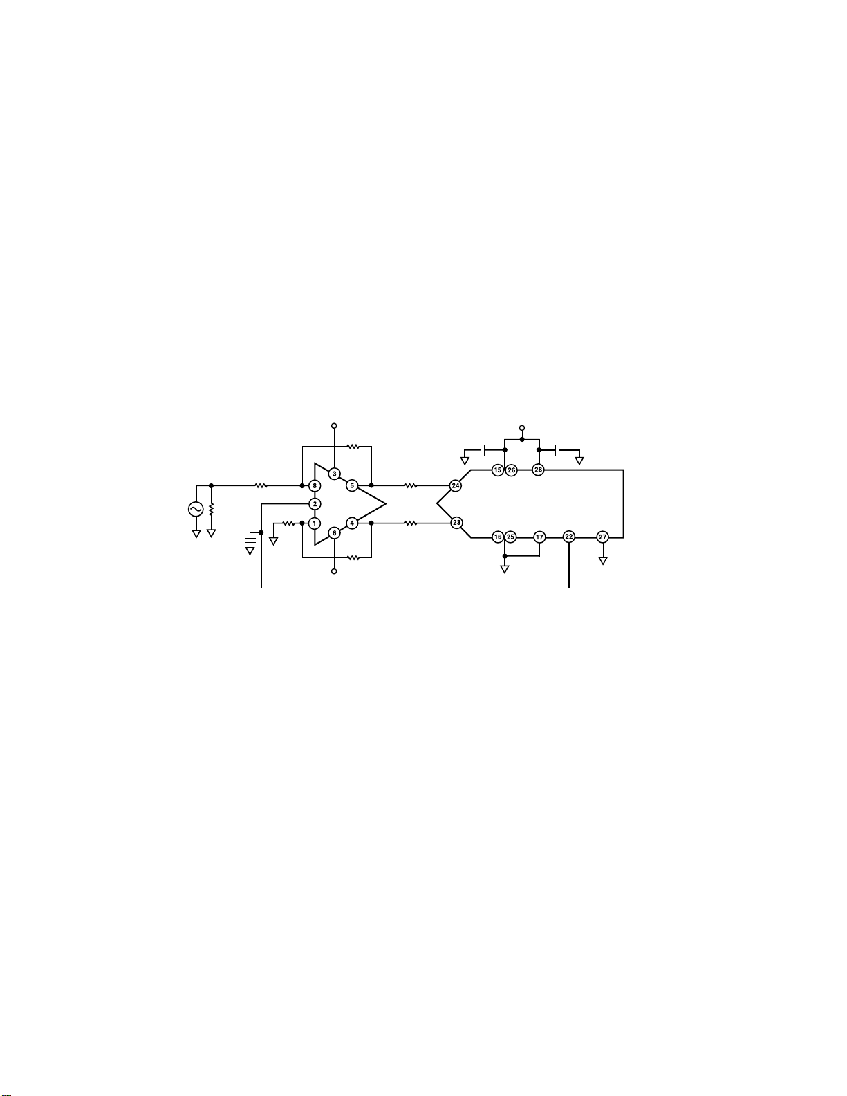
PIN FUNCTION DESCRIPTIONS
Pin No. Name Function
1 –IN Negative Input Summing Node.
2V
Voltage applied to this pin sets the common-
OCM
mode output voltage with a ratio of 1:1. For
example, +1 V dc on V
will set the dc
OCM
bias level on +OUT and –OUT to +1 V.
3 V+ Positive Supply Voltage.
4 +OUT Positive Output. Note: the voltage at –D
is
IN
inverted at +OUT.
5 –OUT Negative Output. Note: the voltage at +D
IN
is inverted at –OUT.
6 V– Negative Supply Voltage.
7 NC No Connect.
8 +IN Positive Input Summing Node
PIN CONFIGURATION
ORDERING GUIDE
Model Temperature Range Package Descriptions Package Options
AD8138AR –40°C to +85°C 8-Lead SOIC SO-8
AD8138AR-REEL
AD8138AR-REEL7
1
2
–40°C to +85°C 13" Tape and Reel SO-8
–40°C to +85°C 7" Tape and Reel SO-8
AD8138-EVAL Evaluation Board
NOTES
1
13" Reels of 2500 each.
2
7" Reels of 750 each.
CAUTION
ESD (electrostatic discharge) sensitive device. Electrostatic charges as high as 4000 V readily
accumulate on the human body and test equipment and can discharge without detection.
WARNING!
Although the AD8138 features proprietary ESD protection circuitry, permanent damage may
occur on devices subjected to high energy electrostatic discharges. Therefore, proper ESD
precautions are recommended to avoid performance degradation or loss of functionality.
ESD SENSITIVE DEVICE
–4–
REV. A
Typical Performance Characteristics–
AD8138
Unless otherwise noted, GAIN = 1, RG = RF = R
6
3
0
GAIN – dB
–3
–6
–9
1
10 100
FREQUENCY – MHz
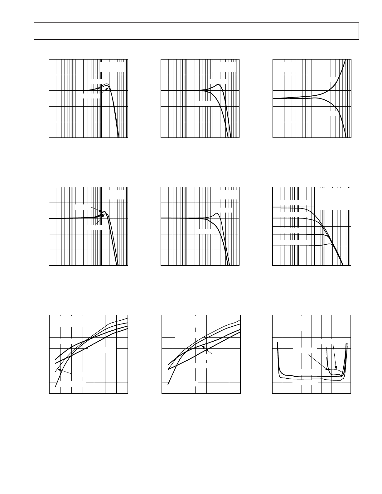
Figure 2. Small Signal Frequency
Response
6
GAIN – dB
–3
–6
3
0
VS = +5V
VS = +5V
VS = 65V
VS = 65V
VIN = 0.2V p-p
= 0pF
C
F
VIN = 2V p-p
= 0pF
C
F
1000
= 499 ⍀, TA = +25ⴗC; Refer to Figure 1 for test setup.
L,dm
GAIN – dB
6
3
0
–3
–6
–9
1
10 100
FREQUENCY – MHz
CF = 0pF
CF = 1pF
VS = 65V
= 0.2V p-p
V
IN
1000
Figure 3. Small Signal Frequency
Response
GAIN – dB
6
3
0
–3
–6
CF = 1pF
VIN = 2V p-p
= 65V
V
S
CF = 0pF
0.5
VS = 65V
= 0.2V p-p
V
IN
0.3
0.1
GAIN – dB
–0.1
–0.3
–0.5
1
10 100
FREQUENCY – MHz
Figure 4. 0.1 dB Flatness vs.
Frequency
30
20
10
GAIN – dB
G = 10, RF = 4.99kV
G = 5, RF = 2.49kV
G = 2, RF = 1kV
G = 1, RF = 499V
0
VS = 65V
C
F
V
OUT
R
G
CF = 0pF
CF = 1pF
= 0pF
= 0.2V p-p
,dm
= 499V
–9
1
10 100
FREQUENCY – MHz
Figure 5. Large Signal Frequency
Response
–50
V
= 2V p-p
,dm
OUT
R
= 800V
L
–60
–70
HD2(VS = +5V)
–80
–90
DISTORTION – dBc
–100
–110
–120
HD3(VS = 65V)
010 70
20 30 40 50 60
FUNDAMENTAL FREQUENCY – MHz
HD2(VS = 65V)
HD3(VS = +5V)
Figure 8. Harmonic Distortion vs.
Frequency
1000
–9
1
10 100
FREQUENCY – MHz
1000
Figure 6. Large Signal Frequency
Response
–40
V
= 4V p-p
,dm
OUT
R
= 800V
L
–50
–60
–70
–80
DISTORTION – dBc
–90
–100
–110
HD3(VS = +5V)
HD2(VS = +5V)
HD2(VS = 65V)
HD3(VS = 65V)
010 70
20 30 40 50 60
FUNDAMENTAL FREQUENCY – MHz
Figure 9. Harmonic Distortion vs.
Frequency
–10
1
10 100
FREQUENCY – MHz
1000
Figure 7. Small Signal Frequency
Response for Various Gains
–30
V
= 2V p-p
,dm
OUT
= 800V
R
L
–40
F
= 20MHz
O
–50
–60
–70
DISTORTION – dBc
–80
–90
–100
–4 –3 3
HD3(VS = +5)
HD3(VS = 65)
HD2(VS = 65)
–2 –1 0 1 2
V
DC OUTPUT – Volts
OCM
HD2(VS = +5)
Figure 10. Harmonic Distortion vs.
V
OCM
4
–5–REV. A
AD8138
p
p
p
–60
VS = 65V
R
–70
–80
–90
–100
DISTORTION – dBc
–110
–120
HD2(F = 20MHz)
0 6
DIFFERENTIAL OUTPUT VOLTAGE – V p-
= 800V
L
HD3(F = 20MHz)
HD2(F = 5MHz)
HD3(F = 5MHz)
54321
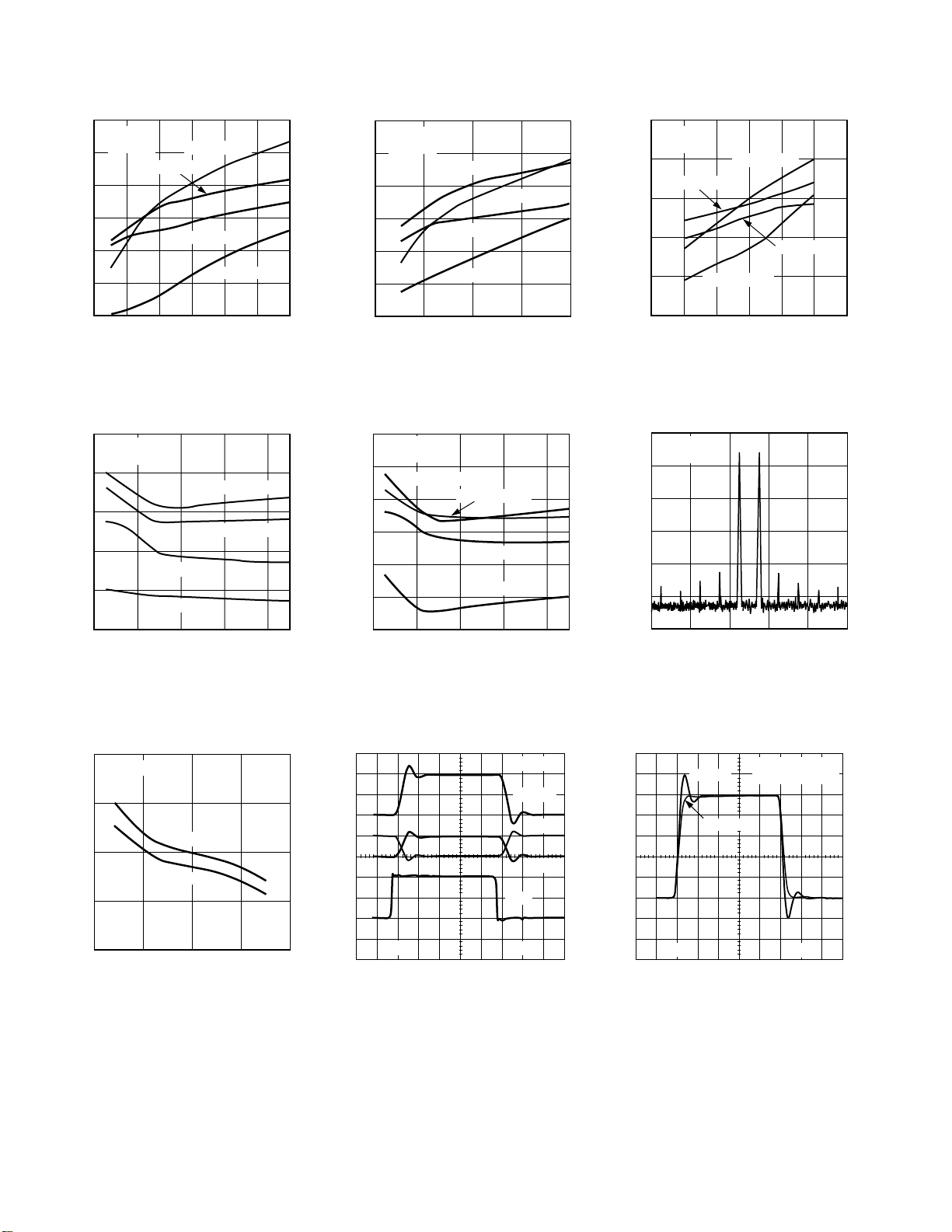
Figure 11. Harmonic Distortion vs.
Differential Output Voltage
–60
VS = +5V
V
= 2V p-p
,dm
OUT
–70
–80
–90
DISTORTION – dBc
–100
–110
200
HD2(F = 5MHz)
HD3(F = 5MHz)
600 1000 1400 1800
R
LOAD
HD2(F = 20MHz)
HD3(F = 20MHz)
– V
Figure 14. Harmonic Distortion vs.
R
LOAD
–60
VS = +5V
R
= 800V
L
–70
–80
–90
–100
DISTORTION – dBc
–110
–120
0
DIFFERENTIAL OUTPUT VOLTAGE – V p-
HD2(F = 20MHz)
HD2(F = 5MHz)
HD3(F = 5MHz)
1
HD3(F = 20MHz)
234
Figure 12. Harmonic Distortion vs.
Differential Output Voltage
–60
VS = 65V
= 2V p-p
V
,dm
OUT
–70
HD2(F = 20MHz)
–80
–90
–100
DISTORTION – dBc
–110
–120
200
600 1000 1400 1800
HD3(F = 20MHz)
HD2(F = 5MHz)
HD3(F = 5MHz)
R
– V
LOAD
Figure 15. Harmonic Distortion vs.
R
LOAD
–60
VS = +3V
= 800V
R
L
–70
HD2(F = 20MHz)
–80
–90
DISTORTION – dBc
–100
–110
0.25
0.50 0.75 1.00 1.25 1.50 1.75
DIFFERENTIAL OUTPUT VOLTAGE – V p-
HD3(F = 20MHz)
HD2(F = 5MHz)
HD3(F = 5MHz)
Figure 13. Harmonic Distortion vs.
Differential Output Voltage
10
FC = 50MHz
= 65V
V
S
–10
–30
–50
– dBm
OUT
P
–70
–90
–110
49.5
49.7 49.9 50.1 50.3 50.5
FREQUENCY – MHz
Figure 16. Intermodulation
Distortion
45
RL = 800V
40
VS = +5V
35
INTERCEPT – dBm
30
25
0
VS = 65V
20
40 60 80
FREQUENCY – MHz
Figure 17. Third Order Intercept vs.
Frequency
VS = 65V
V
OUT,dm
V
V
1V
V
+DIN
5ns
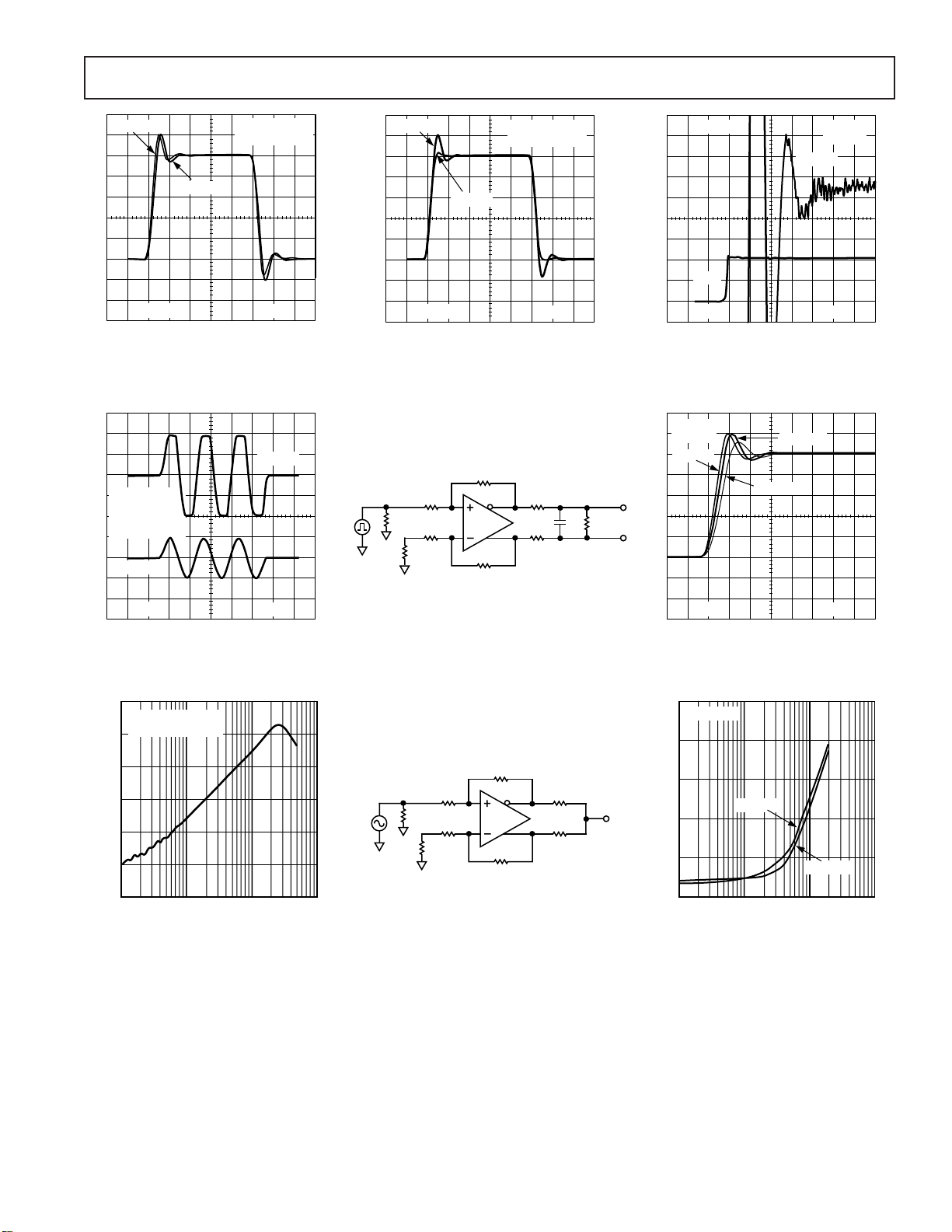
Figure 18. Large Signal Transient
Response
–6–
OUT–
OUT+
V
= 0.2V p-p
CF = 0pF
CF = 1pF
40mV
OUT,dm
V
= 65V
S
5ns
Figure 19. Small Signal Transient
Response
REV. A
VS = 65V
VS = +5V
V
OUT,dm
= 0pF
C
F
= 2V p-p
CF = 0pF
CF = 1pF
V
OUT,dm
V
S
= 65V
= 2V p-p
V
200mV
+DIN
AD8138
VS = 65V
= 1pF
C
F
V
OUT,dm
400mV
5ns
Figure 20. Large Signal Transient
Response
V
OUT,dm
VS = 65V
F = 20MHz
V
= 8V p-p
+DIN
G = 3(R
= 1500)
F
V
+DIN
4V
30ns
Figure 23. Output Overdrive
–20
VS = 65V
DV
/DV
OUT,dm
–30
–40
–50
CMRR – dB
–60
–70
IN,cm
400mV
5ns
Figure 21. Large Signal Transient
Response
499V
49.9V
499V
499V
24.9V
AD8138
499V
24.9V
24.9V
C
453V
L
Figure 24. Test Circuit for Cap Load
Drive
499V
49.9V
499V
499V
24.9V
AD8138
499V
249V
249V
1V
4ns
Figure 22. Settling Time
VS = 65V
C
= 0pF
F
CL = 5pF
400mV
CL = 10pF
CL = 20pF
2.5ns
Figure 25. Large Signal Transient
Response for Various Cap Loads
–20
VIN = 2V p-p
–30
–40
–50
BALANCE ERROR – dB
–60
VS = 65V
VS = +5V
–80
11k10 100
FREQUENCY – MHz
Figure 26. CMRR vs. Frequency
Figure 27. Test Circuit for Output
Balance
–7–REV. A
–70
11k10 100
FREQUENCY – MHz
Figure 28. Output Balance Error vs.
Frequency

AD8138
–10
DV
/DV
OUT,dm
–20
–30
–40
–50
PSRR – dB
–60
–70
–80
–90
11k10 100
S
–PSRR
(V
= 65V)
S
FREQUENCY – MHz
+PSRR
(V
= +5V, 0V AND 65V)
S
Figure 29. PSRR vs. Frequency
5
4
VS = 65V, +5V
3
BIAS CURRENT – mA
2
VS = +3V
100
SINGLE-ENDED OUTPUT
10
VS = +5
IMPEDANCE – V
1
VS = 65V
0.1
1 10 100
FREQUENCY – MHz
Figure 30. Output Impedance vs.
Frequency
30
25
20
15
SUPPLY CURRENT – mA
10
VS = 65V
VS = +5V
VS = +3V
5.0
2.5
VS = 65V
0
–2.5
DIFFERENTIAL OUTPUT OFFSET – mV
–5.0
–40 –20 100
VS = +5V
VS = +3V
0204060 80
TEMPERATURE – 8C
Figure 31. Output Referred Differential Offset Voltage vs. Temperature
GAIN – dB
6
3
0
–3
–6
VS = +5V
VS = 65V
1
–40 –20 100
0204060 80
TEMPERATURE – 8C
Figure 32. Input Bias Current vs.
Temperature
5
–40 –20 100
0204060 80
TEMPERATURE – 8C
Figure 33. Supply Current vs.
Temperature
VS = 65V
V
= –1V TO +1V
OCM
V
400mV
Figure 35. V
Transient Response
OCM
OUT,cm
5ns
–9
11k
Figure 34. V
10 100
FREQUENCY – MHz
Frequency Response
OCM
–8–
REV. A

AD8138
OPERATIONAL DESCRIPTION
Definition of Terms
C
F
R
F
R
+IN
+D
V
OCM
–D
G
IN
IN
–IN
R
G
AD8138
R
F
C
F
–OUT
+OUT
R
L,dm
V
,dm
OUT
Figure 36. Circuit Definitions
Differential voltage refers to the difference between two node
voltages. For example, the output differential voltage (or
equivalently output differential-mode voltage) is defined as:
V
V
+OUT
and V
= (V
OUT,dm
refer to the voltages at the +OUT and –OUT
–OUT
+OUT
– V
–OUT
)
terminals with respect to a common reference.
Common-mode voltage refers to the average of two node voltages. The output common-mode voltage is defined as:
V
OUT,cm
= (V
+OUT
+ V
–OUT
)/2
Balance is a measure of how well differential signals are matched
in amplitude and exactly 180 degrees apart in phase. Balance is
most easily determined by placing a well-matched resistor divider between the differential voltage nodes and comparing the
magnitude of the signal at the divider’s midpoint with the magnitude of the differential signal. (See Figure 27.) By this definition,
output balance is the magnitude of the output common-mode
voltage divided by the magnitude of the output differentialmode voltage:
V
OUT cm
Output Balance Error
=
V
OUT dm
,
,
THEORY OF OPERATION
The AD8138 differs from conventional op amps in that it has
two outputs whose voltages move in opposite directions. Like an
op amp, it relies on high open loop gain and negative feedback
to force these outputs to the desired voltages. The AD8138 behaves much like a standard voltage feedback op amp and makes
it easy to perform single-ended-to-differential conversion,
common-mode level-shifting, and amplification of differential
signals. Also like an op amp, the AD8138 has high input impedance and low output impedance.
Previous differential drivers, both discrete and integrated designs, have been based on using two independent amplifiers,
and two independent feedback loops, one to control each of the
outputs. When these circuits are driven from a single-ended
source, the resulting outputs are typically not well balanced.
Achieving a balanced output has typically required exceptional
matching of the amplifiers and feedback networks.
DC common-mode level-shifting has also been difficult with
previous differential drivers. Level-shifting has required the use
of a third amplifier and feedback loop to control the output
common-mode level. Sometimes the third amplifier has also
been used to attempt to correct an inherently unbalanced
circuit. Excellent performance over a wide frequency range has
proven difficult with this approach.
The AD8138 uses two feedback loops to separately control the
differential and common-mode output voltages. The differential
feedback, set with external resistors, controls only the differential output voltage. The common-mode feedback controls only
the common-mode output voltage. This architecture makes it
easy to arbitrarily set the output common-mode level. It is forced,
by internal common-mode feedback, to be equal to the voltage
applied to the V
input, without affecting the differential
OCM
output voltage.
The AD8138 architecture results in outputs that are very highly
balanced over a wide frequency range without requiring tightly
matched external components. The common-mode feedback
loop forces the signal component of the output common-mode
voltage to be zeroed. The result is nearly perfectly balanced
differential outputs, of identical amplitude and exactly 180
degrees apart in phase.
Analyzing an Application Circuit
The AD8138 uses high open-loop gain and negative feedback to
force its differential and common-mode output voltages in such
a way as to minimize the differential and common-mode error
voltages. The differential error voltage is defined as the voltage
between the differential inputs labeled +IN and –IN in Figure
36. For most purposes, this voltage can be assumed to be zero.
Similarly, the difference between the actual output commonmode voltage and the voltage applied to V
can also be as-
OCM
sumed to be zero. Starting from these two assumptions, any
application circuit can be analyzed.
Setting the Closed Loop Gain
Neglecting the capacitors CF, the differential mode gain of the
circuit in Figure 36 can be determined to be described by the
following equation:
V
,
OUT dm
V
,
IN dm
This assumes the input resistors, R
S
on each side are equal.
R
F
S
R
F
=
S
R
G
S
and feedback resistors,
G
Estimating the Output Noise Voltage
Similar to the case of a conventional op amp, the differential
output errors (noise and offset voltages) can be estimated by
multiplying the input referred terms, at +IN and –IN, by the
circuit noise gain. The noise gain is defined as:
R
G
=+
N
F
1
R
G
To compute the total output referred noise for the circuit of
Figure 36, consideration must also be given to the contribution
of the resistors R
and RG. Refer to Table I for estimated output
F
noise voltage densities at various closed-loop gains.
Table I
RGR
Gain (⍀)(⍀) –3 dB 8138 Only 8138 + RG, R
Bandwidth Output Noise Output Noise
F
F
1 499 499 320 MHz 10 nV/√Hz 11.5 nV/√Hz
2 499 1.0 k 180 MHz 15 nV/√Hz 16.6 nV/√Hz
5 499 2.49 k 70 MHz 30 nV/√Hz 31.6 nV/√Hz
10 499 4.99 k 30 MHz 55 nV/√Hz 56.6 nV/√Hz
–9–REV. A

AD8138
The Impact of Mismatches in the Feedback Networks
As mentioned previously, even if the external feedback networks
(R
) are mismatched, the internal common-mode feedback
F/RG
loop will still force the outputs to remain balanced. The amplitudes of the signals at each output will remain equal and 180
degrees out of phase. The input-to-output differential-mode
gain will vary proportionately to the feedback mismatch, but the
output balance will be unaffected.
Ratio matching errors in the external resistors will result in a
degradation of the circuit’s ability to reject input common-mode
signals, much the same as for a four-resistor difference amplifier
made from a conventional op amp.
Also, if the dc levels of the input and output common-mode
voltages are different, matching errors will result in a small
differential-mode output offset voltage. For G = 1 case, with a
ground referenced input signal and the output common-mode
level set for 2.5 V, an output offset of as much as 25 mV (1% of
the difference in common-mode levels) can result if 1% tolerance resistors are used. Resistors of 1% tolerance will result in a
worst case input CMRR of about 40 dB, worst case differential
mode output offset of 25 mV due to 2.5 V level-shift, and no
significant degradation in output balance error.
Calculating an Application Circuit’s Input Impedance
The effective input impedance of a circuit such as that in Figure
36, at +D
and –DIN, will depend on whether the amplifier is
IN
being driven by a single-ended or differential signal source. For
balanced differential input signals, the input impedance (R
between the inputs (+D
and –DIN) is simply:
IN
R
= 2 × R
IN,dm
G
IN
,dm)
In the case of a single-ended input signal, (for example if –DIN is
grounded and the input signal is applied to +D
), the input
IN
impedance becomes:
R
IN dm
,
=
1
R
G
R
−
2
F
RR
×+
()
GF
The circuit’s input impedance is effectively higher than it would
be for a conventional op amp connected as an inverter because a
fraction of the differential output voltage appears at the inputs
as a common-mode signal, partially bootstrapping the voltage
across the input resistor R
Input Common-Mode Voltage Range in Single Supply
Applications
.
G
The AD8138 is optimized for level-shifting “ground” referenced
input signals. For a single-ended input this would imply, for
example, that the voltage at –D
in Figure 1 would be zero
IN
volts when the amplifier’s negative power supply voltage (at V–)
was also set to zero volts.
Setting the Output Common-Mode Voltage
The AD8138’s V
pin is internally biased at a voltage ap-
OCM
proximately equal to the midsupply point (average value of the
voltages on V+ and V–). Relying on this internal bias will result
in an output common-mode voltage that is within about 100 mV
of the expected value.
In cases where more accurate control of the output commonmode level is required, it is recommended that an external
source, or resistor divider (made up of 10 kΩ resistors), be used.
The output common-mode offset specified on pages 2 and 3
assume the V
input is driven by a low impedance voltage
OCM
source.
Driving a Capacitive Load
A purely capacitive load can react with the pin and bondwire
inductance of the AD8138 resulting in high frequency ringing in
the pulse response. One way to minimize this effect is to place a
small capacitor across each of the feedback resistors. The added
capacitance should be small to avoid destabilizing the amplifier.
An alternative technique is to place a small resistor in series with
the amplifier’s outputs as shown in Figure 24.
LAYOUT, GROUNDING AND BYPASSING
As a high speed part, the AD8138 is sensitive to the PCB environment in which it has to operate. Realizing its superior specifications requires attention to various details of good high speed
PCB design.
The first requirement is for a good solid ground plane that covers as much of the board area around the AD8138 as possible.
The only exception to this is that the two input pins (Pins 1 and
8) should be kept a few mm from the ground plane, and ground
should be removed from inner layers and the opposite side of
the board under the input pins. This will minimize the stray
capacitance on these nodes and help preserve the gain flatness
vs. frequency.
The power supply pins should be bypassed as close as possible
to the device to the nearby ground plane. Good high frequency
ceramic chip capacitors should be used. This bypassing should
be done with a capacitance value of 0.01 µF to 0.1 µF for each
supply. Further away, low frequency bypassing should be pro-
vided with 10 µF tantalum capacitors from each supply to
ground.
The signal routing should be short and direct in order to avoid
parasitic effects. Wherever there are complementary signals, a
symmetrical layout should be provided to the extent possible to
maximize the balance performance. When running differential
signals over a long distance, the traces on PCB should be close
together or any differential wiring should be twisted together to
minimize the area of the loop that is formed. This will reduce
the radiated energy and make the circuit less susceptible to
interference.
–10–
REV. A

BALANCED TRANSFORMER DRIVER
PRIMARY
C
STRAY
C
STRAY
NO SIGNAL IS COUPLED
ON THIS SIDE
SIGNAL WILL BE COUPLED
ON THIS SIDE VIA C
STRAY
52.3V
SECONDARY V
DIFF
500V
0.005%
500V
0.005%
V
UNBAL
Transformers are among the oldest devices that have been used
to perform a single-ended-to-differential conversion (and vice
versa). Transformers also can perform the additional functions
of galvanic isolation, step-up or step-down of voltages and impedance transformation. For these reasons, transformers will
always find uses in certain applications.
However, when driving a transformer single-endedly and then
looking at its output, there is a fundamental imbalance due to
the parasitics inherent in the transformer. The primary (or
driven) side of the transformer has one side at dc potential (usually ground), while the other side is driven. This can cause problems in systems that require good balance of the transformer’s
differential output signals.
If the interwinding capacitance (C
) is assumed to be uni-
STRAY
formly distributed, a signal from the driving source will couple
to the secondary output terminal that is closest to the primary’s
driven side. On the other hand, no signal will be coupled to the
opposite terminal of the secondary, because its nearest primary
terminal is not driven. (See Figure 37.) The exact amount of
this imbalance will depend on the particular parasitics of the
transformer, but will mostly be a problem at higher frequencies.
The balance of a differential circuit can be measured by connecting an equal-valued resistive voltage divider across the differential outputs and then measuring the center point of the
circuit with respect ground. Since the two differential outputs
are supposed to be of equal amplitude, but 180 degrees opposite
phase, there should be no signal present for perfectly balanced
outputs.
The circuit in Figure 37 shows a Minicircuits T1-6T transformer connected with its primary driven single-endedly and the
secondary connected with a precision voltage divider across its
terminals. The voltage divider is made up of two 500 Ω, 0.005%
precision resistors. The voltage V
, which is also equal to
UNBAL
the ac common-mode voltage, is a measure of how closely the
outputs are balanced.
The plots in Figure 39 show a comparison between the case
where the transformer is driven single-endedly by a signal generator and driven differentially using an AD8138. The top signal
trace of Figure 39 shows the balance of the single-ended configuration, while the bottom shows the differentially driven
balance response. The 100 MHz balance is 35 dB better when
using the AD8138.
The well-balanced outputs of the AD8138 will provide a drive
signal to each of the transformer’s primary inputs that are of
equal amplitude and 180 degrees out of phase. Thus, depending
on how the polarity of the secondary is connected, the signals
that conduct across the interwinding capacitance will either both
assist the transformer’s secondary signal equally, or both buck
the secondary signals. In either case, the parasitic effect will be
symmetrical and provide a well-balanced transformer output.
(See Figure 39.)
AD8138
Figure 37. Transformer Single-Ended-to-Differential Converter Is Inherently Imbalanced
499V
C
49.9V
499V
499V
+IN
–IN
499V
OUT–
AD8138
OUT+
49.9V
Figure 38. AD8138 Forms a Balanced Transformer Driver
0
–20
V
, FOR TRANSFORMER
–40
–60
–80
OUTPUT BALANCE ERROR – dB
–100
0.3 500
UNBAL
WITH SINGLE-ENDED DRIVE
1 10 100
FREQUENCY – MHz
Figure 39. Output Balance Error for Circuits of Figures 37
and 38
STRAY
C
STRAY
V
, DIFFERENTIAL DRIVE
UNBAL
V
UNBAL
500V
0.005%
500V
0.005%
V
DIFF
–11–REV. A
AD8138
HIGH PERFORMANCE ADC DRIVING
The circuit in Figure 40 shows a simplified front-end connection for an AD8138 driving an AD9224, a 12-bit, 40 MSPS
A/D converter. The A/D works best when driven differentially,
which minimizes its distortion as described in its data sheet.
The AD8138 eliminates the need for a transformer to drive the
ADC and performs single-ended-to-differential conversion,
common-mode level-shifting and buffering of the driving signal.
The positive and negative outputs of the AD8138 are connected
to the respective differential inputs of the AD9224 via a pair of
49.9 Ω resistors to minimize the effects of the switched-capaci-
tor front-end of the AD9224. For best distortion performance it
is run from supplies of ±5 V.
The AD8138 is configured with unity gain for a single-ended
input-to-differential output. The additional 23 Ω, 523 Ω total,
at the input to –IN is to balance the parallel impedance of the
50 source and its 50 Ω termination that drives the noninverting
input.
+5V
499V
49.9V
49.9V
500V
SOURCE
49.9V
0.1pF
499V
523V
+
V
OCM
AD8138
499V
The signal generator has a ground-referenced, bipolar output,
i.e., it drives symmetrically above and below ground. Connecting V
to the CML pin of the AD9224 sets the output com-
OCM
mon- mode of the AD8138 at 2.5 V, which is the midsupply
level for the AD9224. This voltage is bypassed by a 0.1 µF
capacitor.
The full-scale analog input range of the AD9224 is set to 4 V p-p,
by shorting the SENSE terminal to AVSS. This has been determined to be the scaling to provide minimum harmonic distortion.
For the AD8138 to swing a 4 V p-p, each output swings 2 V p-p,
while providing signals that are 180 degrees out of phase. With a
common-mode voltage at the output of 2.5 V, this means that
each AD8138 output will swing between 1.5 V and 3.5 V
A ground-referenced 4 V p-p, 5 MHz signal at D
+ was used
IN
to test the circuit in Figure 40. When the combined-device
circuit was run with a sampling rate of 20 MHz MSPS, the
SFDR (spurious free dynamic range) was measured at –85 dBc.
+5V
0.1pF 0.1pF
VINB
VINA
DRVDDAVDD
AD9224
AVSS DRVSS
SENSE CML
DIGITAL
OUTPUTS
–5V
Figure 40. AD8138 Driving an AD9224, a 12-Bit, 40 MSPS A/D Converter
–12–
REV. A

AD8138
FREQUENCY – MHz
–40
0
THD – dBc
5 10152025
–45
–50
–55
–60
–65
–70
–75
–80
AD8138-2V
AD8138-1V
FREQUENCY – MHz
65
0
SINAD – dBc
5 10152025
63
61
59
57
55
53
51
45
49
47
AD8138-1V
AD8138-2V
3 V OPERATION
The circuit in Figure 41 shows a simplified front end connection
for an AD8138 driving an AD9203, a 10-bit, 40 MSPS A/D
converter that is specified to work on a single +3 V supply. The
A/D works best when driven differentially to make the best use
of the signal swing available within the 3 V supply. The appropriate outputs of the AD8138 are connected to the appropriate
differential inputs of the AD9203 via a low-pass filter.
The AD8138 is configured for unity gain for a single-ended
input-to-differential output. The additional 23 Ω at the input to
–IN is to balance the impedance of the 50 Ω source and its 50 Ω
termination that drives the noninverting input.
The signal generator has ground-referenced, bipolar output, i.e.,
it can drive symmetrically above and below ground. Even
though the AD8138 has ground as its negative supply, it can
still function as a level-shifter with such an input signal.
The output common-mode is raised up to midsupply by the
voltage divider that biases V
. In this way, the AD8138 pro-
OCM
vides dc-coupling and level-shifting of a bipolar signal, without
inverting the input signal.
The low-pass filter between the AD8138 and the AD9203 provides filtering that helps to improve the signal-to-noise ratio.
Lower noise can be realized by lowering the pole frequency, but
the bandwidth of the circuit will be lowered.
The circuit was tested with a –0.5 dBFS signal at various frequencies. Figure 42 shows a plot of the total harmonic distortion (THD) vs. frequency at signal amplitudes of 1 V and 2 V
differential drive levels.
Figure 43 shows the signal to noise plus distortion (SINAD)
under the same conditions as above. For the smaller signal
swing, the AD8138 performance is quite good, but its performance degrades when trying to swing too close to the supply
rails.
0.1mF
10kV
49.9V
10kV
0.1mF
499V
523V
+3V
499V
+
AD8138
499V
0.1mF 0.1mF
49.9V
20pF
49.9V
20pF
+3V
AINN
AD9203
AINP
AVSS DRVSS
DRVDDAVDD
DIGITAL
OUTPUTS
Figure 41. AD8138 Driving an AD9203, a 10-Bit, 40 MSPS
A/D Converter
Figure 42. AD9203 THD @ –0.5 dBFS AD8138
Figure 43. AD9203 SINAD @ –0.5 dBFS AD8138
–13–REV. A

AD8138
0.1574 (4.00)
0.1497 (3.80)
PIN 1
0.0098 (0.25)
0.0040 (0.10)
OUTLINE DIMENSIONS
Dimensions shown in inches and (mm).
8-Lead SOIC
(SO-8)
0.1968 (5.00)
0.1890 (4.80)
8
5
0.2440 (6.20)
41
0.2284 (5.80)
0.0688 (1.75)
0.0532 (1.35)
0.0196 (0.50)
0.0099 (0.25)
C3581a–0–9/99
x 45°
SEATING
PLANE
0.0500
(1.27)
BSC
0.0192 (0.49)
0.0138 (0.35)
0.0098 (0.25)
0.0075 (0.19)
8°
0°
0.0500 (1.27)
0.0160 (0.41)
–14–
PRINTED IN U.S.A.
REV. A
 Loading...