Analog Devices AD7997 8 Datasheet
8-Channel, 10- and 12-Bit ADCs with I2C-
Compatible Interface in 20-Lead TSSOP
FEATURES
10- and 12-bit ADC with fast conversion time: 2 µs typ
8 single-ended analog input channels
Specified for V
Low power consumption
Fast throughput rate: up to 188 kSPS
Sequencer operation
Automatic cycle mode
2
C®-compatible serial interface supports standard, fast,
I
and high speed modes
Out-of-range indicator/alert function
Pin-selectable addressing via AS
Shutdown mode: 1 µA max
Temperature range: −40°C to +85°C
20-lead TSSOP package
See the AD7992 and AD7994 for 2-channel and 4-channel
equivalent devices, respectively
GENERAL DESCRIPTION
The AD7997/AD7998 are 8-channel, 10- and 12-bit, low power,
successive approximation ADCs with an I
interface. The parts operate from a single 2.7 V to 5.5 V power
supply and feature a 2 µs conversion time. The parts contain an
8-channel multiplexer and track-and-hold amplifier that can
handle input frequencies up to 11 MHz.
The AD7997/AD7998 provide a 2-wire serial interface that is
compatible with I
AD7997-0/AD7998-0 and AD7997-1/AD7998-1, and each
version allows at least two different I
interface on the AD7997-0/AD7998-0 supports standard and
2
C interface modes. The I2C interface on the AD7997-1/
fast I
AD7998-1 supports standard, fast, and high speed I
modes.
The AD7997/AD7998 normally remain in a shutdown state
while not converting, and power up only for conversions. The
conversion process can be controlled using the
by a command mode where conversions occur across I
operations or an automatic conversion interval mode selected
through software control.
The AD7997/AD7998 require an external reference that should
be applied to the REF
. This allows the widest dynamic input range to the ADC.
V
DD
of 2.7 V to 5.5 V
DD
2
C-compatible
2
C interfaces. Each part comes in two versions,
2
C addresses. The I2C
2
C interface
CONVST
2
C write
pin and can be in the range of 1.2 V to
IN
pin,
AD7997/AD7998
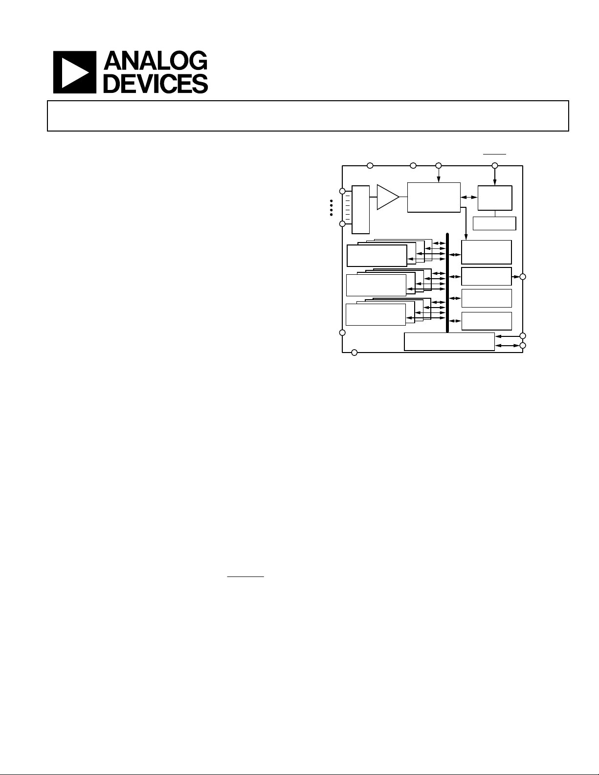
FUNCTIONAL BLOCK DIAGRAM
V
DD
AD7997/AD7998
VIN1
VIN8
REGISTER CH1–CH4
REGISTER CH1–CH4
REGISTER CH1–CH4
AS
AGND
8:1
I/P
MUX
DATA
LOW
DATA
HIGH
HYSTERESIS
T/H
LIMIT
LIMIT
On-chip limit registers can be programmed with high and
low limits for the conversion result, and an open-drain, out-ofrange indicator output (ALERT) becomes active when the
programmed high or low limits are violated by the conversion
result. This output can be used as an interrupt.
PRODUCT HIGHLIGHTS
1. 2 µs conversion time with low power consumption.
2
2. I
C-compatible serial interface with pin-selectable
addresses. Two AD7997/AD7998 versions allow five
AD7997/AD7998 devices to be connected to the same
serial bus.
3. The parts feature automatic shutdown while not converting
to maximize power efficiency. Current consumption is 1 µA
max when in shutdown mode at 3V.
4. Reference can be driven up to the power supply.
5. Out-of-range indicator that can be software disabled or
enabled.
6. One-shot and automatic conversion rates.
7. Registers store minimum and maximum conversion
results.
REF
AGND
10-/12-BIT
SUCCESSIVE
APPROXIMATION
ADC
I2C INTERFACE
Figure 1.
IN
CONFIGURATION
CONVST
CONTROL
LOGIC
OSCILLATOR
CONVERSION
RESULT
REGISTER
REGISTER
ALERT STATUS
REGISTER
CYCLE TIMER
REGISTER
ALERT/BUSY
SCL
SDA
03473-0-001
Rev. 0
Information furnished by Analog Devices is believed to be accurate and reliable.
However, no responsibility is assumed by Analog Devices for its use, nor for any
infringements of patents or other rights of third parties that may result from its use.
Specifications subject to change without notice. No license is granted by implication
or otherwise under any patent or patent rights of Analog Devices. Trademarks and
registered trademarks are the property of their respective owners.
One Technology Way, P.O. Box 9106, Norwood, MA 02062-9106, U.S.A.
Tel: 781.329.4700
Fax: 781.326.8703 © 2004 Analog Devices, Inc. All rights reserved.
www.analog.com

AD7997/AD7998
TABLE OF CONTENTS
AD7997 Specifications..................................................................... 3
AD7998 Specifications..................................................................... 5
2
I
C Timing Specifications................................................................ 7
Absolute Maximum Ratings............................................................ 9
ESD Caution.................................................................................. 9
Pin Configuration and Pin Function Descriptions.................... 10
Te r m in o l o g y .................................................................................... 11
Typical Performance Characteristics........................................... 12
Circuit Information........................................................................ 15
Converter Operation.................................................................. 15
Typical C o n nec t i o n D iagr a m ................................................... 16
Analog Input ............................................................................... 16
Internal Register Structure ............................................................ 18
Address Pointer Register ...........................................................18
Configuration Register .............................................................. 19
Serial Bus Address...................................................................... 23
Writing to the AD7997/AD7998 .................................................. 24
Writing to the Address Pointer Register for a Subsequent
.............................................................................................. 24
Read
Writing a Single Byte of Data to the Alert Status Register or
Cycle Register
Writing Two Bytes of Data to a Limit, Hysteresis, or
Configuration Register
Reading Data from the AD7997/AD7998................................... 26
ALERT/BUSY Pin .......................................................................... 27
SMBus ALERT ............................................................................ 27
BUSY ............................................................................................ 27
Placing the AD7997-1/AD7998-1 into High Speed Mode ... 27
The Address Select (AS) Pin ..................................................... 27
Modes of Operation ....................................................................... 28
Mode 1—Using the
.............................................................................. 24
.............................................................. 24
CONVST
Pin ........................................... 28
Conversion Result Register....................................................... 20
Limit Registers ............................................................................ 20
Alert Status Register (CH1 to CH4) ........................................ 21
Cycle Timer Register.................................................................. 22
Sample Delay and Bit Trial Delay............................................. 22
Serial Interface ................................................................................ 23
REVISION HISTORY
9/04—Revision 0: Initial Version
Mode 2 – COMMAND MODE ............................................... 29
Mode 3—Automatic Cycle Interval Mode.............................. 30
Outline Dimensions....................................................................... 31
Ordering Guide .......................................................................... 31
Related Parts in I
2
C-Compatible ADC Product Family........ 31
Rev. 0 | Page 2 of 32
AD7997/AD7998
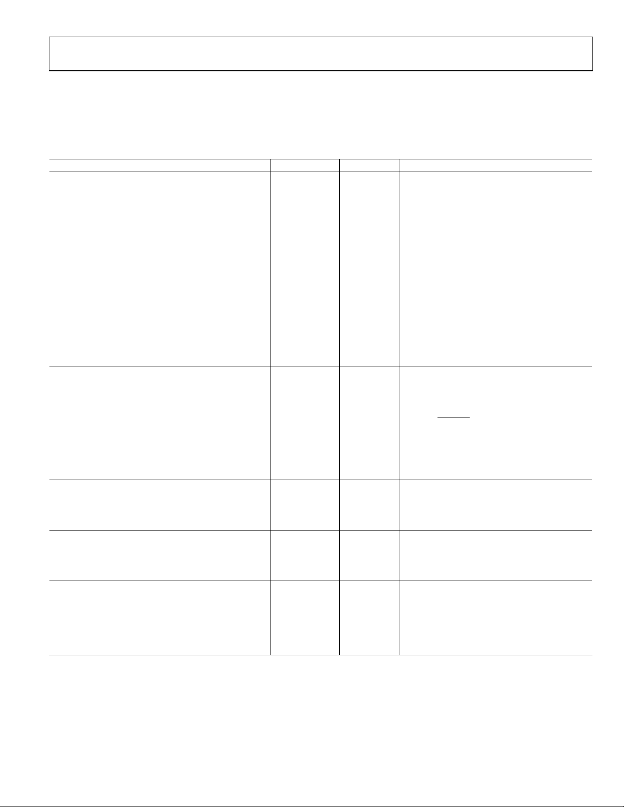
AD7997 SPECIFICATIONS
Temperature range for B version is −40°C to +85°C. Unless otherwise noted, VDD = 2.7 V to 5.5 V; REFIN = 2.5 V; For the AD7997-0, all
specifications apply for f
T
= T
to T
A
MIN
MAX
.
up to 400 kHz; for the AD7997-1, all specifications apply for f
SCL
Table 1.
Parameter B Version Unit Test Conditions/Comments
DYNAMIC PERFORMANCE1
Signal to Noise + Distortion (SINAD)2 61 dB min
Total Harmonic Distortion (THD) 2 –75 dB max
Peak Harmonic or Spurious Noise (SFDR) 2 –76 dB max
Intermodulation Distortion (IMD)
2
Second-Order Terms –86 dB typ
Third-Order Terms –86 dB typ
Aperture Delay2 10 ns max
Aperture Jitter2 50 ps typ
Channel-to-Channel Isolation2 –90 dB typ FIN = 108 Hz, see the Terminology section
Full-Power Bandwidth2 11 MHz typ @ 3 dB
2 MHz typ @ 0.1 dB
DC ACCURACY
Resolution 10 Bits
Integral Nonlinearity
Differential Nonlinearity
1, 2
±0.5 LSB max
1, 2
±0.5 LSB max Guaranteed no missed codes to 10 bits
Offset Error2 ±1.5 LSB max
±2.5 LSB max Mode 2 (Command Mode)
Offset Error Match2 ±0.5 LSB max
Gain Error
2
±1.5 LSB max
Gain Error Match2 ±0.5 LSB max
ANALOG INPUT
Input Voltage Range 0 to REF
IN
V
DC Leakage Current ±1 µA max
Input Capacitance 30 pF typ
REFERENCE INPUT
REFIN Input Voltage Range 1.2 to VDD V min/V max
DC Leakage Current ±1 µA max
Input Impedance 69 kΩ typ During a conversion
LOGIC INPUTS (SDA, SCL)
Input High Voltage, V
Input Low Voltage, V
0.7 (VDD) V min
INH
0.3 (VDD) V max
INL
Input Leakage Current, IIN ±1 µA max VIN = 0 V or VDD
Input Capacitance, C
Input Hysteresis, V
3
IN
0.1 (VDD) V min
HYST
10 pF max
up to 3.4 MHz, unless otherwise noted;
SCL
= 10 kHz sine wave for f
F
IN
from 1.7 MHz to
SCL
3.4 MHz
= 1 kHz sine wave for f
F
IN
fa = 10.1 kHz, fb = 9.9 kHz for f
up to 400 kHz
SCL
from 1.7 MHz
SCL
to 3.4 MHz
fa = 1.1 kHz, fb = 0.9 kHz for f
Mode 1 (
CONVST Mode)
up to 400 kHz
SCL
Rev. 0 | Page 3 of 32

AD7997/AD7998
Parameter B Version Unit Test Conditions/Comments
LOGIC INPUTS (CONVST)
Input High Voltage, V
2.4 V min VDD = 5 V
INH
2.0 V min VDD = 3 V
Input Low Voltage, V
0.8 V max VDD = 5 V
INL
0.4 V max VDD = 3 V
Input Leakage Current, IIN ±1 µA max VIN = 0 V or V
Input Capacitance, C
3
10 pF max
IN
LOGIC OUTPUTS (OPEN-DRAIN)
Output Low Voltage, VOL 0.4 V max I
0.6 V max I
Floating-State Leakage Current ± 1 µA max
Floating-State Output Capacitance
3
Output Coding Straight (Natural) Binary
CONVERSION RATE See the Modes of Operation section
Conversion Time 2 µs typ
Throughput Rate
Mode 1 (Reading after the Conversion) 5 kSPS typ f
21 kSPS typ f
121 kSPS typ f
Mode 2 5.5 kSPS typ f
22 kSPS typ f
147 kSPS typ f
POWER REQUIREMENTS
V
DD
I
DD
Power-Down Mode, Interface Inactive 1/2 µA max VDD = 3.3 V/5.5 V
Power-Down Mode, Interface Active 0.07/0.3 mA max VDD = 3.3 V/5.5 V, 400 kHz f
0.3/0.6 mA max VDD = 3.3 V/5.5 V, 3.4 MHz f
Operating, Interface Inactive 0.06/0.1 mA max VDD = 3.3 V/5.5 V, 400 kHz f
0.3/0.6 mA max VDD = 3.3 V/5.5 V, 3.4 MHz f
Operating, Interface Active 0.15/0.4 mA max VDD = 3.3 V/5.5 V, 400 kHz f
0.6/1.1 mA max VDD = 3.3 V/5.5 V, 3.4 MHz f
0.7/1.4 mA typ VDD = 3.3 V/5.5 V, 3.4 MHz f
Mode 3 (I2C Inactive, T
x 32) 0.7/1.5 mA max VDD = 3.3 V/5.5 V
CONVERT
Power Dissipation
Fully Operational
Operating, Interface Active 0.495/2.2 mW max VDD = 3.3 V/5.5 V, 400 kHz f
1.98/6.05 mW max VDD = 3.3 V/5.5 V, 3.4 MHz f
2.31/7.7 mW typ VDD = 3.3 V/5.5 V, 3.4 MHz f
Power Down, Interface Inactive 3.3/11 µW max VDD = 3.3 V/5.5 V
1
Max/min ac dynamic performance, INL and DNL specifications are typical specifications when operating in Mode 2 with I2C Hs-Mode SCL frequencies. Specifications
outlined for Mode 2 apply to Mode 3 also. Sample delay and bit trial delay enabled.
2
See the Terminology section.
3
Guaranteed by initial characterization.
DD
= 3 mA
SINK
= 6 mA
SINK
10 pF max
= 100 kHz
SCL
= 400 kHz
SCL
= 3.4 MHz
SCL
= 100 kHz
SCL
= 400 kHz
SCL
= 3.4 MHz, 188 kSPS typ @ 5 V
SCL
2.7/5.5 V min/max
Digital inputs = 0 V or V
DD
SCL
SCL
SCL
SCL
SCL
Mode 1
SCL
Mode 2
SCL
SCL
Mode 1
SCL
Mode 2
SCL
Rev. 0 | Page 4 of 32
AD7997/AD7998
AD7998 SPECIFICATIONS
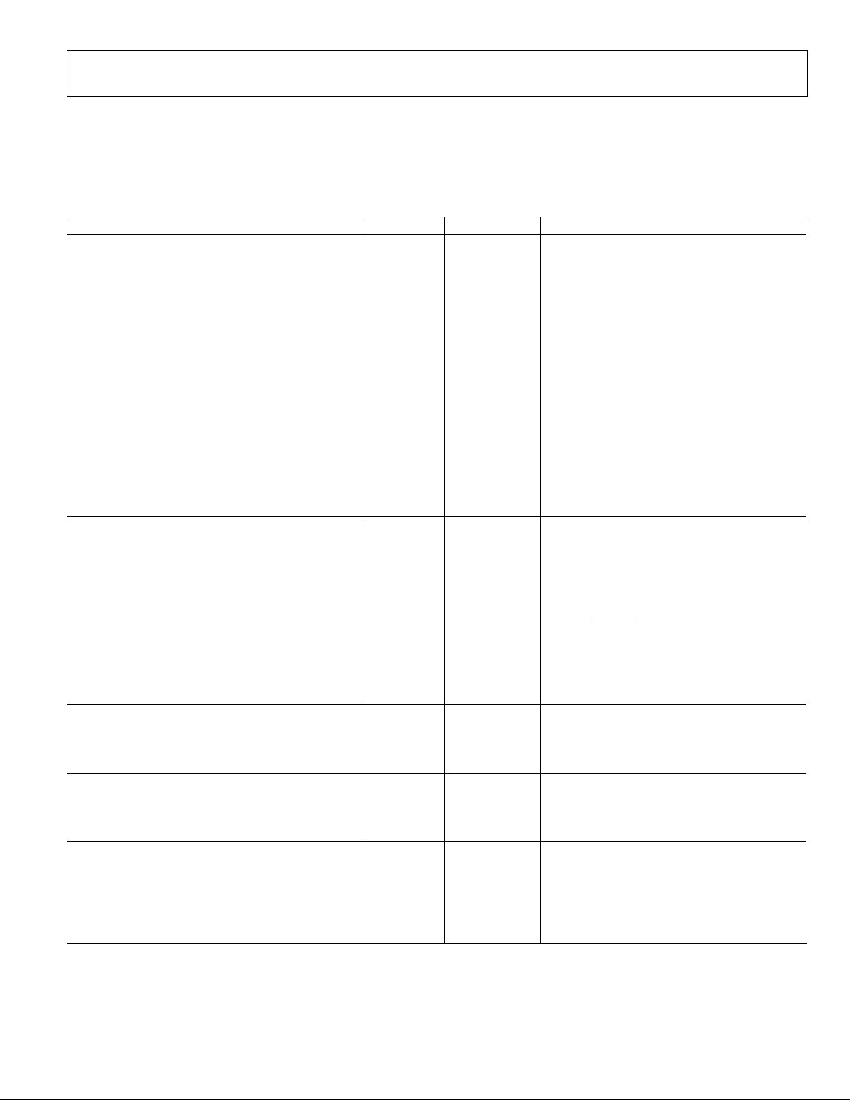
Temperature range for B version is −40°C to +85°C. Unless otherwise noted, VDD = 2.7 V to 5.5 V; REFIN = 2.5 V; For the AD7998-0, all
specifications apply for f
T
= T
to T
A
MIN
MAX
.
up to 400 kHz; for the AD7998-1, all specifications apply for f
SCL
Table 2.
Parameter B Version Unit Test Conditions/Comments
DYNAMIC PERFORMANCE1
Signal-to-Noise + Distortion (SINAD)2 70.5 dB min
Signal to Noise Ratio (SNR)
2
71 dB min
Total Harmonic Distortion (THD)2 –78 dB max
Peak Harmonic or Spurious Noise (SFDR)2 –79 dB max
Intermodulation Distortion (IMD)2
Second-Order Terms –90 dB typ
Third-Order Terms –90 dB typ
Aperture Delay2 10 ns max
Aperture Jitter2 50 ps typ
Channel-to-Channel Isolation2 –90 dB typ FIN = 108 Hz, see the Terminology section
Full-Power Bandwidth2 11 MHz typ @ 3 dB
2 MHz typ @ 0.1 dB
DC ACCURACY
Resolution 12 Bits
Integral Nonlinearity
1,2
±1 LSB max
±0.2 LSB typ
Differential Nonlinearity
1,2
+1/–0.9 LSB max Guaranteed no missed codes to 12 bits
±0.2 LSB typ
Offset Error2 ±4 LSB max
±6 LSB max Mode 2 (Command Mode)
Offset Error Match2 ±1 LSB max
Gain Error2 ±2 LSB max
Gain Error Match2 ±1 LSB max
ANALOG INPUT
Input Voltage Range 0 to REF
V
IN
DC Leakage Current ± 1 µA max
Input Capacitance 30 pF typ
REFERENCE INPUT
REFIN Input Voltage Range 1.2 to V
DD
V min/V max
DC Leakage Current ± 1 µA max
Input Impedance 69 kΩ typ
LOGIC INPUTS (SDA, SCL)
Input High Voltage, V
Input Low Voltage, V
0.7 (VDD) V min
INH
0.3 (VDD) V max
INL
Input Leakage Current, IIN ± 1 µA max VIN = 0 V or V
Input Capacitance, C
Input Hysteresis, V
3
IN
0.1 (VDD) V min
HYST
10 pF max
up to 3.4 MHz, unless otherwise noted;
SCL
= 10 kHz sine wave for f
F
IN
from 1.7 MHz to
SCL
3.4 MHz
= 1 kHz sine wave for f
F
IN
fa = 10.1 kHz, fb = 9.9 kHz f
up to 400 kHz
SCL
from 1.7 MHz to
SCL
3.4 MHz
fa = 1.1 kHz, fb = 0.9 kHz for f
Mode 1 (
CONVST Mode)
DD
up to 400 kHz
SCL
Rev. 0 | Page 5 of 32
AD7997/AD7998
Parameter B Version Unit Test Conditions/Comments
LOGIC INPUTS (CONVST)
Input High Voltage, V
2.4 V min VDD = 5 V
INH
2.0 V min VDD = 3 V
Input Low Voltage, V
0.8 V max VDD = 5 V
INL
0.4 V max VDD = 3 V
Input Leakage Current, IIN ±1 µA max VIN = 0 V or V
Input Capacitance, C
3
10 pF max
IN
LOGIC OUTPUTS (OPEN-DRAIN)
Output Low Voltage, VOL 0.4 V max I
0.6 V max I
Floating-State Leakage Current ±1 µA max
Floating-State Output Capacitance3 10 pF max
Output Coding Straight (Natural) Binary
CONVERSION RATE See the Modes of Operation section
Conversion Time 2 µs typ
Throughput Rate
Mode 1 (Reading after the Conversion) 5 kSPS typ f
21 kSPS typ f
121 kSPS typ f
Mode 2 5.5 kSPS typ f
22 kSPS typ f
147 kSPS typ f
POWER REQUIREMENTS
V
DD
I
DD
Power-Down Mode, Interface Inactive 1/2 µA max VDD = 3.3 V/5.5 V
Power-Down Mode, Interface Active 0.07/0.3 mA max VDD = 3.3 V/5.5 V, 400 kHz f
0.3/0.6 mA max VDD = 3.3 V/5.5 V, 3.4 MHz f
Operating, Interface Inactive 0.06/0.1 mA max VDD = 3.3 V/5.5 V, 400 kHz f
0.3/0.6 mA max VDD = 3.3 V/5.5 V, 3.4 MHz f
Operating, Interface Active 0.15/0.4 mA max VDD = 3.3 V/5.5 V, 400 kHz f
0.6/1.1 mA max VDD = 3.3 V/5.5 V, 3.4 MHz f
0.7/1.4 mA typ VDD = 3.3 V/5.5 V, 3.4 MHz f
Mode 3 (I2C Inactive, T
x 32) 0.7/1.5 mA max VDD = 3.3 V/5.5 V
CONVERT
Power Dissipation
Fully Operational
Operating, Interface Active 0.495/2.2 mW max VDD = 3.3 V/5.5 V, 400 kHz f
1.98/6.05 mW max VDD = 3.3 V/5.5 V, 3.4 MHz f
2.31/7.7 mW typ VDD = 3.3 V/5.5 V, 3.4 MHz f
Power Down, Interface Inactive 3.3/11 µW max VDD = 3.3 V/5.5 V
1
Max/min ac dynamic performance, INL and DNL specifications are typical specifications when operating in Mode 2 with I2C Hs-Mode SCL frequencies. Specifications
outlined for Mode 2 apply to Mode 3 also. Sample delay and bit trial delay enabled.
2
See the section. Terminology
3
Guaranteed by initial characterization.
DD
= 3 mA
SINK
= 6 mA
SINK
= 100 kHz
SCL
= 400 kHz
SCL
= 3.4 MHz
SCL
= 100 kHz
SCL
= 400 kHz
SCL
= 3.4 MHz , 188 kSPS typ @ 5 V
SCL
2.7/5.5 V min/max
Digital inputs = 0 V or V
DD
SCL
SCL
SCL
SCL
SCL
Mode 1
SCL
Mode 2
SCL
SCL
Mode 1
SCL
Mode 2
SCL
Rev. 0 | Page 6 of 32
AD7997/AD7998
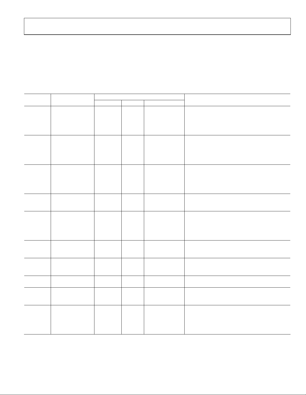
I2C TIMING SPECIFICATIONS
Guaranteed by initial characterization. All values measured with input filtering enabled. CB refers to capacitive load on the bus line. tr and
measured between 0.3 VDD and 0.7 VDD.
t
f
High speed mode timing specifications apply to the AD7997-1/AD7998-1 only. Standard and fast mode timing specifications apply to
both the AD7997-0/AD7998-0 and the AD7997-1/AD7998-1. See Figure 2. Unless otherwise noted, V
=T
to T
T
A
MIN
MAX
.
Table 3.
AD7997/AD7998 Limit at T
Parameter Conditions Min Max Unit Description
f
Standard mode 100 kHz Serial clock frequency
SCL
Fast mode 400 kHz
High speed mode
C
C
= 100 pF max 3.4 MHz
B
= 400 pF max 1.7 MHz
B
t1 Standard mode 4 µs t
Fast mode 0.6 µs
High speed mode
C
C
= 100 pF max 60 ns
B
= 400 pF max 120 ns
B
t2 Standard mode 4.7 µs t
Fast mode 1.3 µs
High speed mode
C
C
= 100 pF max 160 ns
B
= 400 pF max 320 ns
B
t3 Standard mode 250 ns t
Fast mode 100 ns
High speed mode 10 ns
1
t
4
Standard mode 0 3.45 µs t
Fast mode 0 0.9 µs
High speed mode
C
C
= 100 pF max 0 70
B
= 400 pF max 0 150 ns
B
2
ns
t5 Standard mode 4.7 µs t
Fast mode 0.6 µs
High speed mode 160 ns
t6 Standard mode 4 µs t
Fast mode 0.6 µs
High speed mode 160 ns
t7 Standard mode 4.7 µs t
Fast mode 1.3 µs
t8 Standard mode 4 µs t
Fast mode 0.6 µs
High speed mode 160 ns
t9 Standard mode 1000 ns t
Fast mode 20 + 0.1 CB 300 ns
High speed mode
C
C
= 100 pF max 10 80 ns
B
= 400 pF max 20 160 ns
B
MIN
, T
MAX
, SCL high time
HIGH
, SCL low time
LOW
, data setup time
SU;DAT
, data hold time
HD;DAT
, setup time for a repeated start condition
SU;STA
, hold time (repeated) start condition
HD;STA
, bus free time between a stop and a start condition
BUF
, setup time for stop condition
SU;STO
, rise time of SDA signal
RDA
= 2.7 V to 5.5 V; REFIN = 2.5 V;
DD
Rev. 0 | Page 7 of 32
AD7997/AD7998
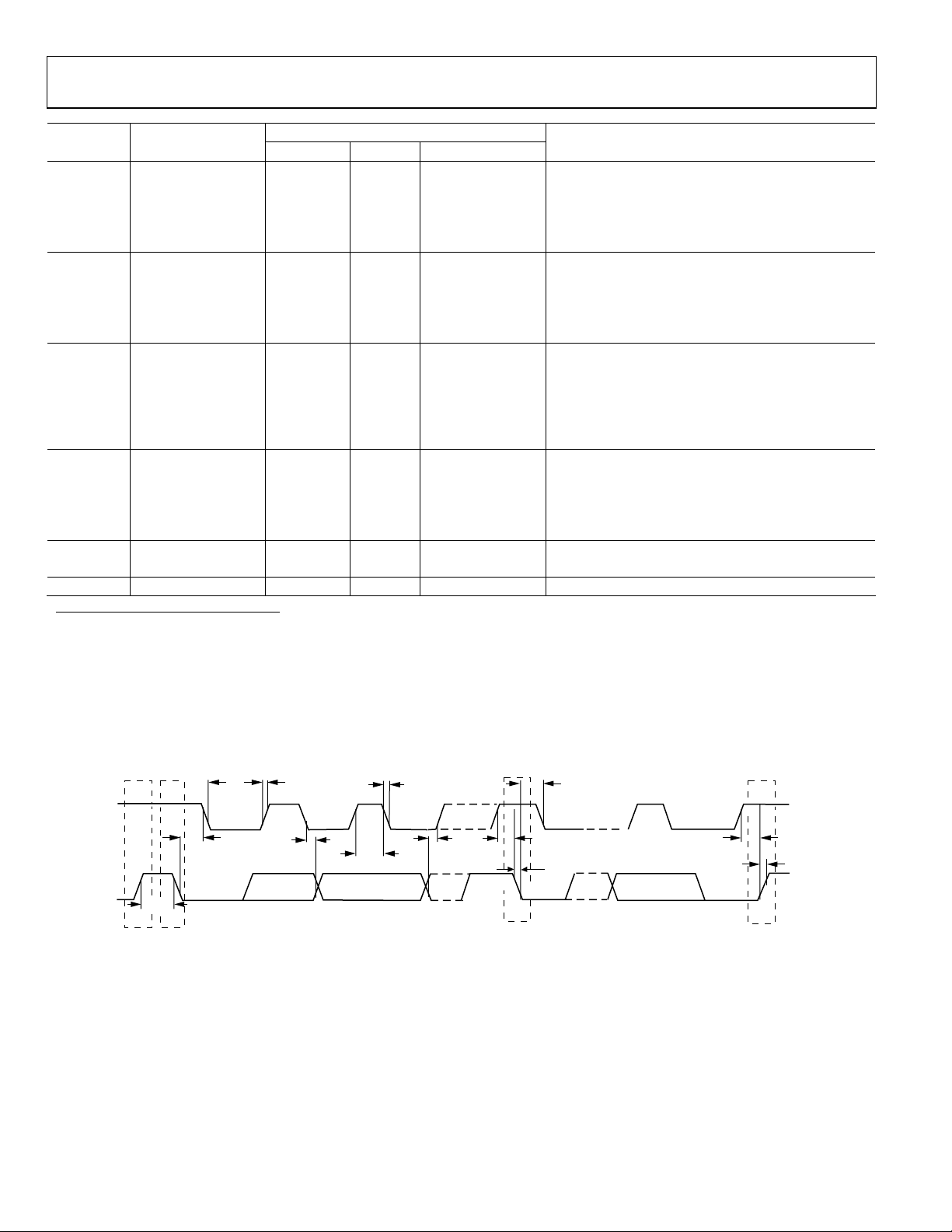
AD7997/AD7998 Limit at T
Parameter Conditions Min Max Unit Description
t
10
Standard mode 300 ns t
Fast mode 20 + 0.1 CB300 ns
High speed mode
C
C
= 100 pF max 10 80 ns
B
= 400 pF max 20 160 ns
B
t11 Standard mode 1000 ns t
Fast mode 20 + 0.1 CB300 ns
High speed mode
C
C
t
11A
= 100 pF max 10 40 ns
B
= 400 pF max 20 80 ns
B
Standard mode 1000 ns t
Fast mode 20 + 0.1 CB300 ns
High speed mode
C
C
t
12
= 100 pF max 10 80 ns
B
= 400 pF max 20 160 ns
B
Standard mode 300 ns t
Fast mode 20 + 0.1 CB 300 ns
High speed mode
C
C
t
SP
= 100 pF max 10 40 ns
B
= 400 pF max 20 80 ns
B
Fast mode 0 50 ns Pulse width of suppressed spike
High speed mode 0 10 ns
t
POWER-UP
1 typ µs Power-up time
1
A device must provide a data hold time for SDA in order to bridge the undefined region of the SCL falling edge.
2
For 3 V supplies, the maximum hold time with CB = 100 pF max is 100 ns max.
MIN
, T
MAX
, fall time of SDA signal
FDA
, rise time of SCL signal
RCL
, rise time of SCL signal after a repeated start
RCL1
condition and after an Acknowledge bit
, fall time of SCL signal
FCL
t
6
t
5
t
10
S
t
8
t
9
P
03473-0-002
SCL
SDA
t
7
P
S = START CONDITION
P = STOP CONDITION
t
11
t
2
t
6
S
t
4
t
12
t
3
t
1
Figure 2. Timing Diagram for 2-Wire Serial Interface
Rev. 0 | Page 8 of 32
AD7997/AD7998
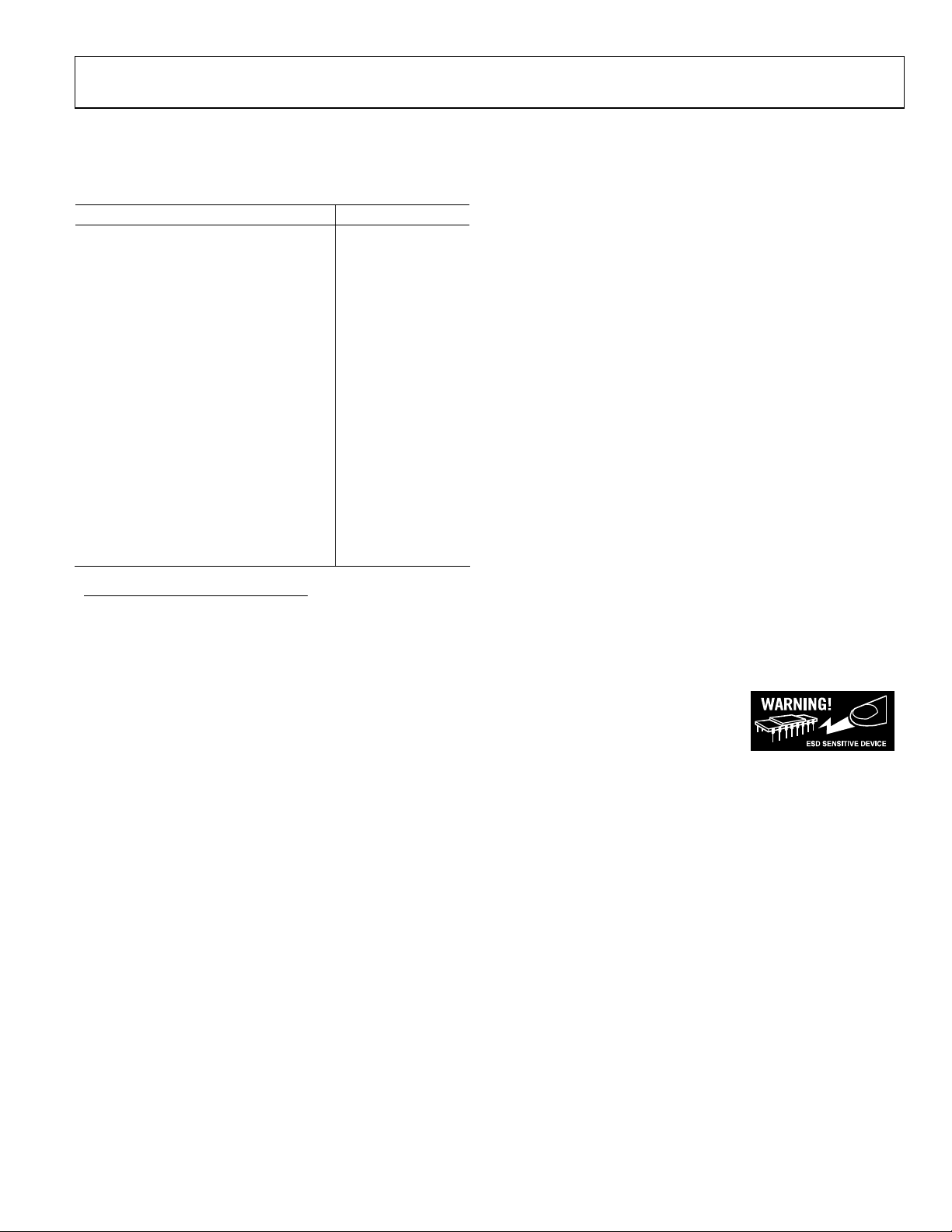
ABSOLUTE MAXIMUM RATINGS
TA = 25°C, unless otherwise noted.
Table 4.
Parameter Rating
VDD to GND −0.3 V to 7 V
Analog Input Voltage to GND −0.3 V to VDD + 0.3 V
Reference Input Voltage to GND −0.3 V to VDD + 0.3 V
Digital Input Voltage to GND −0.3 V to +7 V
Digital Output Voltage to GND −0.3 V to VDD + 0.3 V
Input Current to Any Pin Except Supplies1±10 mA
Operating Temperature Range
Commercial (B Version) −40°C to +85°C
Storage Temperature Range −65°C to +150°
Junction Temperature 150°C
20-Lead TSSOP
θJA Thermal Impedance 143°C/W
θJC Thermal Impedance 45°C/W
Pb/SN Temperature, Soldering
Reflow (10 s to 30 s) 240 (+0/-5)°C
Pb-free Temperature, Soldering
Reflow 260 (+0)°C
ESD 1.5 kV
1
Transient currents of up to 100 mA do not cause SCR latch-up.
Stresses above those listed under Absolute Maximum Ratings
may cause permanent damage to the device. This is a stress
rating only; functional operation of the device at these or any
other conditions above those listed in the operational sections
of this specification is not implied. Exposure to absolute
maximum rating conditions for extended periods may affect
device reliability.
ESD CAUTION
ESD (electrostatic discharge) sensitive device. Electrostatic charges as high as 4000 V readily accumulate on
the human body and test equipment and can discharge without detection. Although this product features
proprietary ESD protection circuitry, permanent damage may occur on devices subjected to high energy
electrostatic discharges. Therefore, proper ESD precautions are recommended to avoid performance
degradation or loss of functionality.
Rev. 0 | Page 9 of 32
AD7997/AD7998
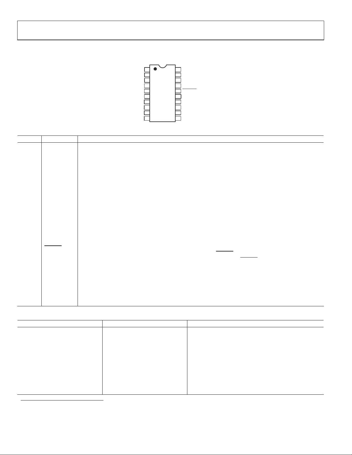
PIN CONFIGURATION AND PIN FUNCTION DESCRIPTIONS
1
AGND
V
2
DD
DD
IN
5
IN
AD7997/
3
AD7998
4
TOP VIEW
(Not to Scale)
5
6
7
8
9
10
AGND
AGND
V
REF
VIN1
VIN3
V
VIN7
Figure 3. AD7998/AD7997 Pin Configuration
20
AGND
SCL
19
SDA
18
ALERT/BUSY
17
CONVST
16
AS
15
VIN2
14
V
4
13
IN
VIN6
12
VIN8
11
03473-0-003
Table 5. Pin Function Descriptions
Pin No. Mnemonic Function
1, 3,
4, 20
AGND Analog Ground. Ground reference point for all circuitry on the AD7997/AD7998. All analog input signals should be
referred to this AGND voltage.
2, 5 VDD Power Supply Input. The VDD range for the AD7997/AD7998 is from 2.7 V to 5.5 V.
6 REFIN Voltage Reference Input. The external reference for the AD7997/AD7998 should be applied to this input pin. The
voltage range for the external reference is 1.2 V to V
. A 0.1 µF and 1 µF capacitors should be placed between REFIN
DD
and AGND. See Typical Connection Diagram.
7 VIN1 Analog Input 1. Single-ended analog input channel. The input range is 0 V to REFIN.
8 VIN3 Analog Input 3. Single-ended analog input channel. The input range is 0 V to REFIN.
9 VIN5 Analog Input 5. Single-ended analog input channel. The input range is 0 V to REFIN.
10 VIN7 Analog Input 7. Single-ended analog input channel. The input range is 0 V to REFIN.
11 VIN8 Analog Input 8. Single-ended analog input channel. The input range is 0 V to REFIN.
12 VIN6 Analog Input 6. Single-ended analog input channel. The input range is 0 V to REFIN.
13 VIN4 Analog Input 4. Single-ended analog input channel. The input range is 0 V to REFIN.
14 VIN2 Analog Input 2. Single-ended analog input channel. The input range is 0 V to REFIN.
15 AS
Logic Input. Address select input that selects one of three I
2
C addresses for the AD7997/AD7998, as shown in Table 6.
The device address depends on the voltage applied to this pin.
16
CONVST
Logic Input Signal. Convert start signal. This is an edge-triggered logic input. The rising edge of this signal powers up
the part. The power-up time for the part is 1 µs. The falling edge of
initiates a conversion. A power-up time of at least 1 µs must be allowed for the
CONVST
places the track/hold into hold mode and
CONVST
high pulse; otherwise, the
conversion result is invalid (see the Modes of Operation section).
17 ALERT/BUSY Digital Output. Selectable as an ALERT or BUSY output function. When configured as an ALERT, this pin acts as an out-
of-range indicator and, if enabled, becomes active when the conversion result violates the DATAHIGH or DATALOW
register values. See the Limit Registers section. When configured as a BUSY output, this pin becomes active when a
conversion is in progress. Open-drain output.
18 SDA Digital I/O. Serial bus bidirectional data. Open-drain output. External pull-up resistor required.
19 SCL Digital Input. Serial bus clock. Open-drain input. External pull-up resistor required.
Table 6. I2C Address Selection
Part Number AS Pin I2C Address
AD7997-0 AGND 010 0001
AD7997-0 VDD 010 0010
AD7997-1 AGND 010 0011
AD7997-1 VDD 010 0100
AD7997-x
1
Float 010 0000
AD7998-0 AGND 010 0001
AD7998-0 VDD 010 0010
AD7998-1 AGND 010 0011
AD7998-1 VDD 010 0100
AD7998-x1
Float 010 0000
1
If the AS pin is left floating on any of the AD7997/AD7998 parts, the device address is 010 0000.
Rev. 0 | Page 10 of 32
 Loading...