ANALOG DEVICES AD7984 Service Manual

18-Bit, 1.33 MSPS PulSAR 10.5 mW
V
V
±
FEATURES
18-bit resolution with no missing codes
Throughput: 1.33 MSPS
Low power dissipation: 10.5 mW at 1.33 MSPS
INL: ±2.25 LSB maximum
Dynamic range: 99.7 dB typical
True differential analog input range: ±V
0 V to V
with V
REF
between 2.9 V to 5.0 V
REF
Allows use of any input range
Easy to drive with the ADA4941
No pipeline delay
Single-supply 2.5 V operation with 1.8 V/2.5 V/3 V/5 V logic
interface
Serial interface SPI-/QSPI™-/MICROWIRE™-/DSP-compatible
Ability to daisy-chain multiple ADCs and busy indicator
10-lead MSOP (MSOP-8 size) and 10-lead 3 mm × 3 mm QFN
(LFCSP), SOT-23 size
APPLICATIONS
Battery-powered equipment
Data acquisition systems
Medical instruments
Seismic data acquisition systems
REF
ADC in MSOP/QFN
AD7984
APPLICATION DIAGRAM
REF
IN+
AD7984
IN–
GND
Figure 1.
2.5
VDD
VIO
SDI
SCK
SDO
CNV
REF
1.8V TO 5V
. The reference voltage,
3- OR 4-WI RE
INTERFACE
(SPI, CS
DAISY CHAIN)
2.9V TO 5
10V, ±5V, ..
ADA4941
GENERAL DESCRIPTION
The AD7984 is an 18-bit, successive approximation, analog-todigital converter (ADC) that operates from a single power
supply, VDD. It contains a low power, high speed, 18-bit
sampling ADC and a versatile serial interface port. On the CNV
rising edge, the AD7984 samples the voltage difference between
the IN+ and IN− pins. The voltages on these pins usually swing
in opposite phases between 0 V and V
REF, is applied externally and can be set independent of the
supply voltage, VDD.
The SPI-compatible serial interface also features the ability,
using the SDI input, to daisy-chain several ADCs on a single
3-wire bus and provides an optional busy indicator. It is compatible
with 1.8 V, 2.5 V, 3 V, and 5 V logic, using the separate VIO supply.
06973-001
The AD7984 is available in a 10-lead MSOP or a 10-lead QFN
(LFCSP) with operation specified from −40°C to +85°C.
Table 1. MSOP, QFN (LFCSP) 14-/16-/18-Bit PulSAR® ADC
Type 100 kSPS 250 kSPS 400 kSPS to 500 kSPS ≥1000 kSPS ADC Dri ver
14-Bit AD7940 AD79421 AD79461
16-Bit AD7680 AD7685
1
AD7686
1
AD79801 ADA4941-x
AD7683 AD76871 AD76881 AD79831 ADA4841-x
AD7684 AD7694 AD76931
18-Bit AD76911 AD76901 AD79821 ADA4941-x
AD79841 ADA4841-x
1
Pin-for-pin compatible.
Rev. A
Information furnished by Analog Devices is believed to be accurate and reliable. However, no
responsibility is assumed by Analog Devices for its use, nor for any infringements of patents or other
rights of third parties that may result from its use. Specifications subject to change without notice. No
license is granted by implication or otherwise under any patent or patent rights of Analog Devices.
Trademarks and registered trademarks are the property of their respective owners.
One Technology Way, P.O. Box 9106, Norwood, MA 02062-9106, U.S.A.
Tel: 781.329.4700 www.analog.com
Fax: 781.461.3113 ©2007–2010 Analog Devices, Inc. All rights reserved.

AD7984
TABLE OF CONTENTS
Features .............................................................................................. 1
Driver Amplifier Choice ........................................................... 14
Applications ....................................................................................... 1
Application Diagram ........................................................................ 1
General Description ......................................................................... 1
Revision History ............................................................................... 2
Specifications ..................................................................................... 3
Timing Specifications .................................................................. 5
Absolute Maximum Ratings ............................................................ 6
ESD Caution .................................................................................. 6
Pin Configurations and Function Descriptions ........................... 7
Typical Performance Characteristics ............................................. 8
Terminolog y .................................................................................... 11
Theory of Operation ...................................................................... 12
Circuit Information .................................................................... 12
Converter Operation .................................................................. 12
Typical Connection Diagram ................................................... 13
Analog Inputs .............................................................................. 14
Single-to-Differential Driver .................................................... 15
Voltage Reference Input ............................................................ 15
Power Supply ............................................................................... 15
Digital Interface .......................................................................... 16
CS
Mode, 3-Wire Without Busy Indicator ............................. 17
CS
Mode, 3-Wire with Busy Indicator .................................... 18
CS
Mode, 4-Wire Without Busy Indicator ............................. 19
CS
Mode, 4-Wire with Busy Indicator .................................... 20
Chain Mode Without Busy Indicator ...................................... 21
Chain Mode with Busy Indicator ............................................. 22
Application Hints ........................................................................... 23
Layout .......................................................................................... 23
Evaluating the AD7984 Performance ...................................... 23
Outline Dimensions ....................................................................... 24
Ordering Guide .......................................................................... 24
REVISION HISTORY
8/10—Rev. 0 to Rev. A
Updated Outline Dimensions ....................................................... 24
Changes to Ordering Guide .......................................................... 24
11/07—Revision 0: Initial Version
Rev. A | Page 2 of 24
AD7984
SPECIFICATIONS
VDD = 2.5 V, VIO = 2.3 V to 5.5 V, REF = 5 V, TA = −40°C to +85°C, unless otherwise noted.
Table 2.
Parameter Conditions Min Typ Max Unit
RESOLUTION 18 Bits
ANALOG INPUT
Voltage Range IN+ − IN− −V
Absolute Input Voltage IN+, IN− −0.1 V
Common-Mode Input Range IN+, IN− V
Analog Input CMRR fIN = 450 kHz 67 dB1
Leakage Current at 25°C Acquisition phase 200 nA
Input Impedance See the Analog Inputs section
ACCURACY
No Missing Codes 18 Bits
Differential Linearity Error −1 +1.5 LSB2
Integral Linearity Error −2.25 +2.25 LSB2
Transition Noise 0.95 LSB2
Gain Error, T
MIN
3
to T
−0.075 ±0.022 +0.075 % of FS
MAX
Gain Error Temperature Drift −0.6 ppm/°C
Zero Error, T
MIN
3
to T
−700 ±100 +700 μV
MAX
Zero Temperature Drift 0.3 ppm/°C
Power Supply Sensitivity
VDD = 2.5 V ± 5%
THROUGHPUT
Conversion Rate 0 1.33 MSPS
Transient Response Full-scale step 290 ns
AC ACCURACY
Dynamic Range V
Signal-to-Noise, SNR fIN = 1 kHz, V
= 5 V 99.7 dB1
REF
= 5 V, TA = 25°C 96.5 98.5 dB1
REF
Spurious-Free Dynamic Range, SFDR fIN = 10 kHz 112.5 dB1
Total Harmonic Distortion4, THD fIN = 10 kHz −110.5 dB1
Signal-to-(Noise + Distortion), SINAD fIN = 10 kHz, V
1
All specifications expressed in decibels are referred to a full-scale input FSR and tested with an input signal at 0.5 dB below full scale, unless otherwise specified.
2
LSB means least significant bit. With the ±5 V input range, one LSB is 38.15 μV.
3
See Terminology section. These specifications include full temperature range variation but not the error contribution from the external reference.
4
Tested fully in production at fIN = 1 kHz.
= 5 V, TA = 25°C 98 dB1
REF
+V
REF
× 0.475 V
REF
× 0.5 V
REF
V
REF
+ 0.1 V
REF
× 0.525 V
REF
90 dB1
Rev. A | Page 3 of 24

AD7984
VDD = 2.5 V, VIO = 2.3 V to 5.5 V, REF = 5 V, TA = −40°C to +85°C, unless otherwise noted.
Table 3.
Parameter Conditions Min Typ Max Unit
REFERENCE
Voltage Range 2.9 5.1 V
Load Current 1.33 MSPS 520 μA
SAMPLING DYNAMICS
−3 dB Input Bandwidth 10 MHz
Aperture Delay 2 ns
DIGITAL INPUTS
Logic Levels
VIL VIO > 3 V –0.3 +0.3 × VIO V
VIH VIO > 3 V 0.7 × VIO VIO + 0.3 V
VIL VIO ≤ 3 V –0.3 +0.1 × VIO V
VIH VIO ≤ 3 V 0.9 × VIO VIO + 0.3 V
IIL −1 +1 μA
IIH −1 +1 μA
DIGITAL OUTPUTS
Data Format Serial 18 bits, twos complement
Pipeline Delay
Conversion results available immediately
after completed conversion
VOL I
VOH I
= +500 μA 0.4 V
SINK
= −500 μA VIO − 0.3 V
SOURCE
POWER SUPPLIES
VDD 2.375 2.5 2.625 V
VIO Specified performance 2.3 5.5 V
VIO Range 1.8 5.5 V
Standby Current
1, 2
VDD and VIO = 2.5 V 1.1 mA
Power Dissipation 1.33 MSPS throughput 10.5 14 mW
Energy per Conversion 7.9 nJ/sample
TEMPERATURE RANGE3
Specified Performance T
1
With all digital inputs forced to VIO or GND as required.
2
During acquisition phase.
3
Contact an Analog Devices, Inc., sales representative for the extended temperature range.
MIN
to T
−40 +85 °C
MAX
Rev. A | Page 4 of 24
AD7984
TIMING SPECIFICATIONS
TA = −40°C to +85°C, VDD = 2.37 V to 2.63 V, VIO = 2.3 V to 5.5 V, unless otherwise noted.1
Table 4.
Parameter Symbol Min Typ Max Unit
Conversion Time: CNV Rising Edge to Data Available t
Acquisition Time t
Time Between Conversions t
CNV Pulse Width (CS Mode)
SCK Period (CS Mode)
VIO Above 4.5 V 10.5 ns
VIO Above 3 V 12 ns
VIO Above 2.7 V 13 ns
VIO Above 2.3 V 15 ns
SCK Period (Chain Mode) t
VIO Above 4.5 V 11.5 ns
VIO Above 3 V 13 ns
VIO Above 2.7 V 14 ns
VIO Above 2.3 V 16 ns
SCK Low Time t
SCK High Time t
SCK Falling Edge to Data Remains Valid t
SCK Falling Edge to Data Valid Delay t
VIO Above 4.5 V 9.5 ns
VIO Above 3 V 11 ns
VIO Above 2.7 V 12 ns
VIO Above 2.3 V 14 ns
CNV or SDI Low to SDO D15 MSB Valid (CS Mode)
VIO Above 3 V 10 ns
VIO Above 2.3 V 15 ns
CNV or SDI High or Last SCK Falling Edge to SDO High Impedance (CS Mode)
SDI Valid Setup Time from CNV Rising Edge t
SDI Valid Hold Time from CNV Rising Edge (CS Mode)
SDI Valid Hold Time from CNV Rising Edge (Chain Mode) t
SCK Valid Setup Time from CNV Rising Edge (Chain Mode) t
SCK Valid Hold Time from CNV Rising Edge (Chain Mode) t
SDI Valid Setup Time from SCK Falling Edge (Chain Mode) t
SDI Valid Hold Time from SCK Falling Edge (Chain Mode) t
SDI High to SDO High (Chain Mode with Busy Indicator) t
1
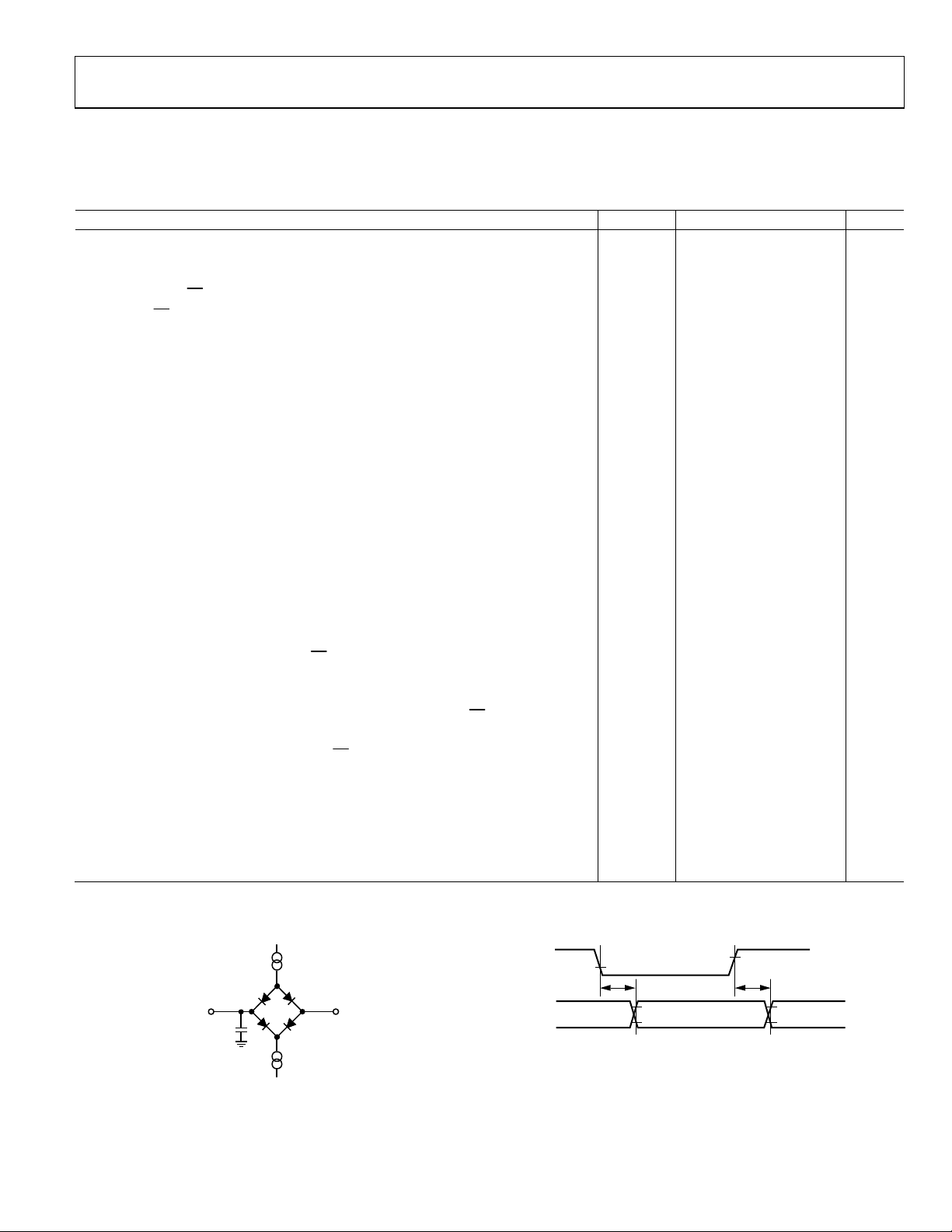
See Figure 2 and Figure 3 for load conditions.
300 500 ns
CONV
250 ns
ACQ
750 ns
CYC
t
10 ns
CNVH
t
SCK
SCK
4.5 ns
SCKL
4.5 ns
SCKH
3 ns
HSDO
DSDO
t
EN
t
20 ns
DIS
5 ns
SSDICNV
t
2 ns
HSDICNV
0 ns
HSDICNV
5 ns
SSCKCNV
5 ns
HSCKCNV
2 ns
SSDISCK
3 ns
HSDISCK
15 ns
DSDOSDI
1
Y% VIO
t
DELAY
V
V
2
IH
2
IL
6973-003
TO SDO
20pF
C
L
500µA I
500µA I
OL
1.4V
OH
6973-002
Figure 2. Load Circuit for Digital Interface Timing
1
X% VIO
t
DELAY
2
V
IH
2
V
IL
1
FOR VIO ≤ 3.0V, X = 90, AND Y = 1 0; FOR VIO > 3.0V, X = 70, AND Y = 30.
2
MINIMUM VIH AND MAXIMUM VIL USED. SEE DIGITAL INPUTS
SPECIFICATIONS IN TABLE 3.
Figure 3. Voltage Levels for Timing
Rev. A | Page 5 of 24
AD7984
ABSOLUTE MAXIMUM RATINGS
Table 5.
Parameter Rating
Analog Inputs
IN+, IN− to GND1
Supply Voltage
REF, VIO to GND −0.3 V to +6.0 V
VDD to GND −0.3 V to +3.0 V
VDD to VIO +3 V to −6 V
Digital Inputs to GND −0.3 V to VIO + 0.3 V
Digital Outputs to GND −0.3 V to VIO + 0.3 V
Storage Temperature Range −65°C to +150°C
Junction Temperature 150°C
θJA Thermal Impedance
10-Lead MSOP 200°C/W
10-Lead QFN (LFCSP) 48.7°C/W
θJC Thermal Impedance
10-Lead MSOP 44°C/W
10-Lead QFN (LFCSP) 2.96°C/W
Lead Temperatures
Vapor Phase (60 sec) 215°C
Infrared (15 sec) 220°C
1
See the Analog Inputs section for an explanation of IN+ and IN−.
−0.3 V to V
or ±130 mA
+ 0.3 V
REF
Stresses above those listed under Absolute Maximum Ratings
may cause permanent damage to the device. This is a stress
rating only; functional operation of the device at these or any
other conditions above those indicated in the operational
section of this specification is not implied. Exposure to absolute
maximum rating conditions for extended periods may affect
device reliability.
ESD CAUTION
Rev. A | Page 6 of 24
AD7984
PIN CONFIGURATIONS AND FUNCTION DESCRIPTIONS
VIO
1
REF
VDD
2
AD7984
3
REF
VDD
IN+
IN–
GND
1
2
AD7984
3
TOP VIEW
(Not to Scale)
4
5
10
VIO
9
SDI
8
SCK
7
SDO
CNV
6
06973-004
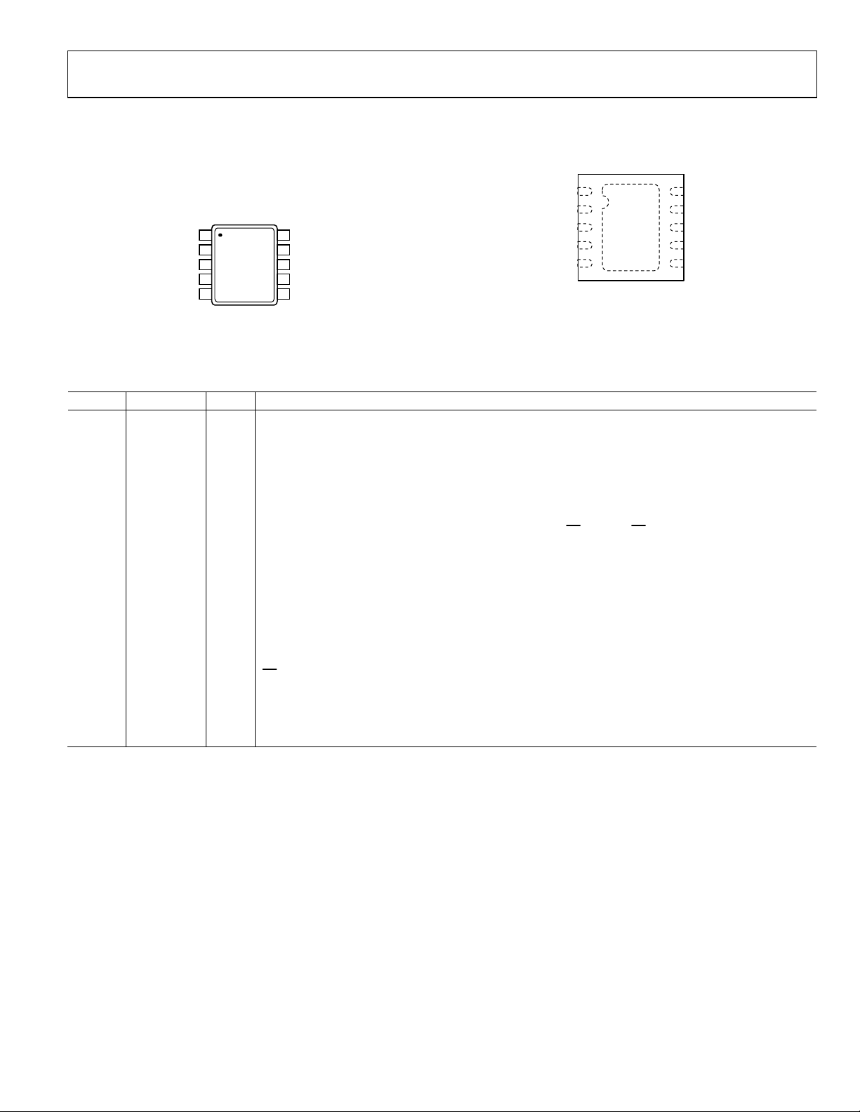
Figure 4. 10-Lead MSOP Pin Configuration
IN+
IN–
GND
*EXPOSED PADDLE CAN BE CONNECTED
TO GROUND.
Figure 5. 10-Lead QFN (LFCSP) Pin Configuration
(EXPOSED
4
5
PAD)*
Table 6. Pin Function Descriptions
Pin No. Mnemonic Type1 Description
1 REF AI
Reference Input Voltage. The REF range is 2.9 V to 5.1 V. This pin is referred to the GND pin and
should be decoupled closely to the GND pin with a 10 μF capacitor.
2 VDD P Power Supply.
3 IN+ AI Differential Positive Analog Input.
4 IN− AI Differential Negative Analog Input.
5 GND P Power Supply Ground.
6 CNV DI
Convert Input. This input has multiple functions. On its rising edge, it initiates the conversions
and selects the interface mode of the part: chain mode or CS mode. In CS mode, the SDO pin is
enabled when CNV is low. In chain mode, the data should be read when CNV is high.
7 SDO DO Serial Data Output. The conversion result is output on this pin. It is synchronized to SCK.
8 SCK DI Serial Data Clock Input. When the part is selected, the conversion result is shifted out by this clock.
9 SDI DI
Serial Data Input. This input provides multiple features. It selects the interface mode of the ADC as
follows:
Chain mode is selected if SDI is low during the CNV rising edge. In this mode, SDI is used as a
data input to daisy-chain the conversion results of two or more ADCs onto a single SDO line. The
digital data level on SDI is output on SDO with a delay of 18 SCK cycles.
CS mode is selected if SDI is high during the CNV rising edge. In this mode, either SDI or CNV can
enable the serial output signals when low. If SDI or CNV is low when the conversion is complete,
the busy indicator feature is enabled.
10 VIO P
Input/Output Interface Digital Power. Nominally at the same supply as the host interface
(1.8 V, 2.5 V, 3 V, or 5 V ).
1
AI = analog input, DI = digital input, DO = digital output, and P = power.
10
SDI
9
SCK
8
SDO
7
CNV
6
06973-005
Rev. A | Page 7 of 24
AD7984
TYPICAL PERFORMANCE CHARACTERISTICS
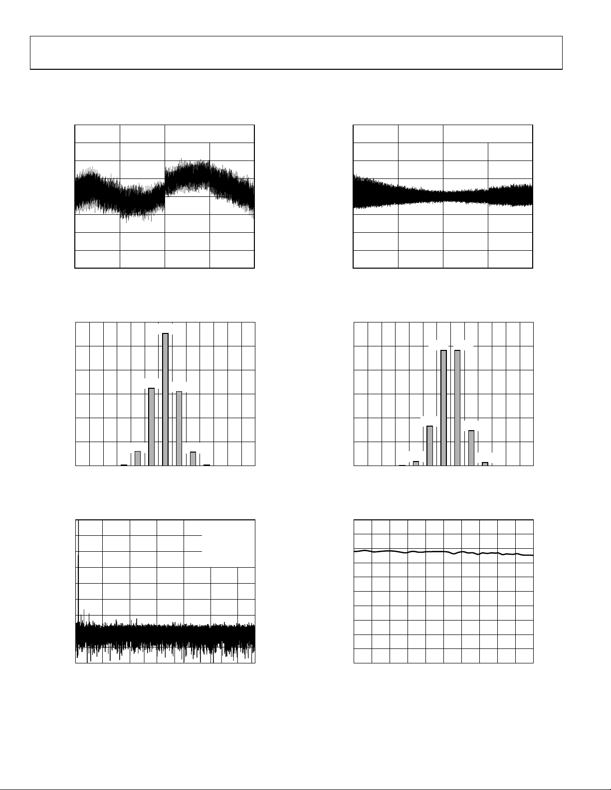
VDD = 2.5 V, REF = 5.0 V, VIO = 3.3 V.
2.0
1.5
POSITIVE I NL: +1. 07LSB
NEGATIVE INL: –0.73LSB
2.0
1.5
POSITIVE DNL: +0.63L SB
NEGATIV E DNL: –0.34LS B
1.0
0.5
0
INL (LSB)
–0.5
–1.0
–1.5
–2.0
0 262144
65536 131072 196608
CODE
Figure 6. Integral Nonlinearity vs. Code
60k
50k
40k
30k
COUNTS
20k
10k
1D 1E
326
1F
007 600
0
1C
55354
32350
31003
5992
20 21 22 23 24 25
CODE IN HEX
5708
326
26 27 28
Figure 7. Histogram of a DC Input at the Code Center
AMPLITUDE (dB of Full Scale)
–20
–40
–60
–80
–100
–120
–140
–160
–180
0
0
100 200 300 400 500 600
FREQUENCY (kHz)
f
= 1.33MSPS
S
f
= 10kHz
IN
SNR = 98.2dB
THD = –110.6dB
SFDR = 112.5dB
SINAD = 98.0d B
Figure 8. FFT Plot
1.0
0.5
0
DNL (LSB)
–0.5
–1.0
–1.5
06973-032
–2.0
0 262144
65536 131072 196608
CODE
06973-038
Figure 9. Differential Nonlinearity vs. Code
60k
16593
1801
CODE IN HEX
48273 48266
14653
1378
00
06973-042
50k
40k
30k
COUNTS
20k
10k
06973-041
002
0
1D
1E 1F
206921 22 23 24 25 26 273728 29
Figure 10. Histogram of a DC Input at the Code Transition
100
99
98
97
96
95
SNR (dB)
94
93
92
91
06973-033
90
–10 0
–9 –8 –7 –6 –5 –4 –3 –2 –1
INPUT LEVEL (dB of Full Scale)
06973-039
Figure 11. SNR vs. Input Level
Rev. A | Page 8 of 24
 Loading...