

Analog Devices AD7863BR-3, AD7863BR-10, AD7863ARS-3, AD7863ARS-2, AD7863ARS-10 Datasheet
...
REV. A
Information furnished by Analog Devices is believed to be accurate and
reliable. However, no responsibility is assumed by Analog Devices for its
use, nor for any infringements of patents or other rights of third parties
which may result from its use. No license is granted by implication or
otherwise under any patent or patent rights of Analog Devices.
a
AD7863
One Technology Way, P.O. Box 9106, Norwood, MA 02062-9106, U.S.A.
Tel: 781/329-4700 World Wide Web Site: http://www.analog.com
Fax: 781/326-8703 © Analog Devices, Inc., 1999
Simultaneous Sampling
Dual 175 kSPS 14-Bit ADC
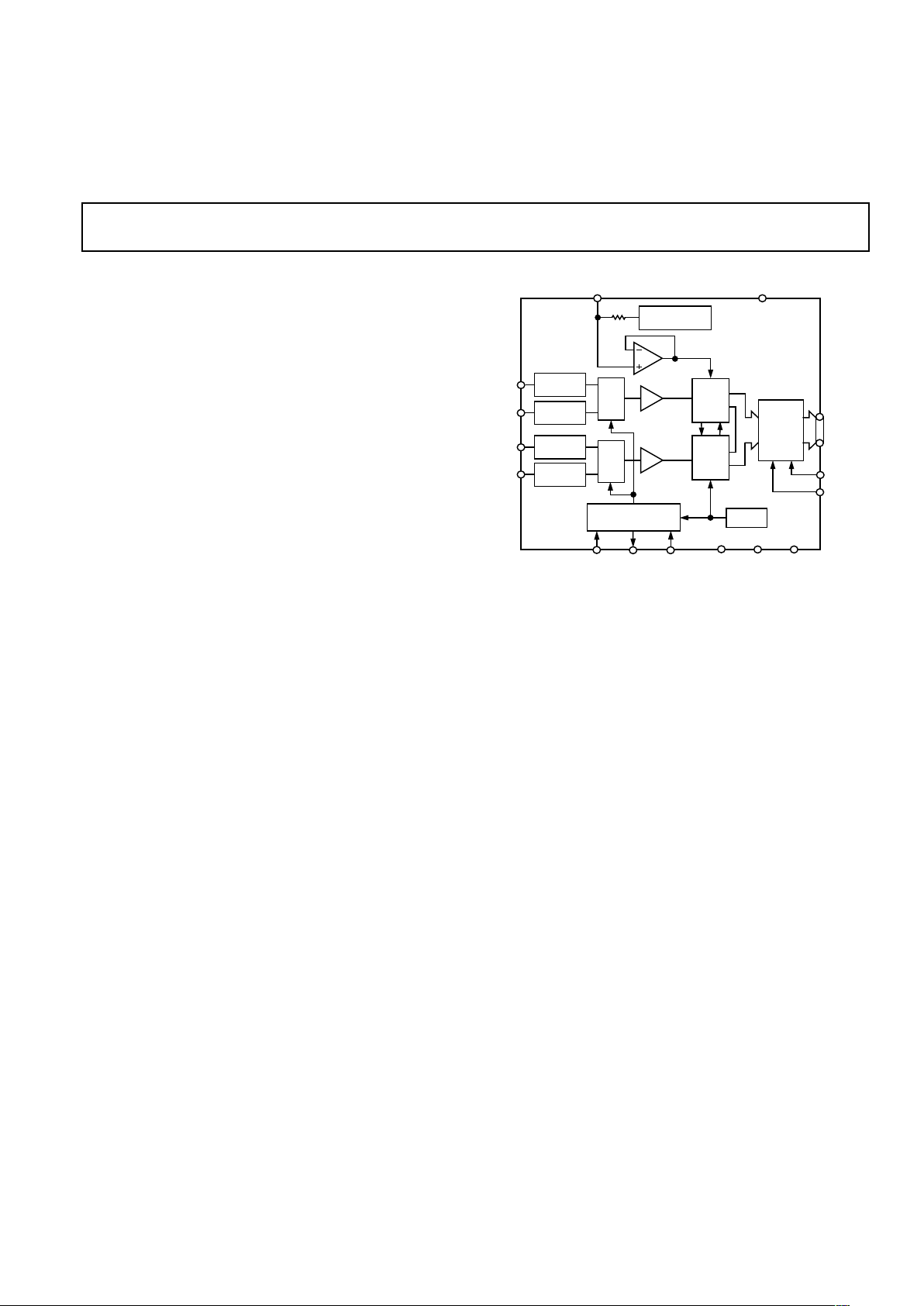
FUNCTIONAL BLOCK DIAGRAM
DGND
DB0
BUSY
CS
CONVST
AD7863
AGND
V
REF
2k
AGND
TRACK/
HOLD
V
DD
DB13
A0
14-BIT
ADC
TRACK/
HOLD
MUX
SIGNAL
SCALING
+2.5V
REFERENCE
OUTPUT
LATCH
RD
CONVERSION
CONTROL LOGIC
SIGNAL
SCALING
SIGNAL
SCALING
SIGNAL
SCALING
MUX
14-BIT
ADC
CLOCK
V
A1
V
B1
V
A2
V
B2
FEATURES
Two Fast 14-Bit ADCs
Four Input Channels
Simultaneous Sampling and Conversion
5.2 s Conversion Time
Single Supply Operation
Selection of Input Ranges
10 V for AD7863-10
2.5 V for AD7863-3
0 V to 2.5 V for AD7863-2
High Speed Parallel Interface
Low Power, 70 mW Typ
Power Saving Mode, 105 W Max
Overvoltage Protection on Analog Inputs
14-Bit Lead Compatible Upgrade to AD7862
APPLICATIONS
AC Motor Control
Uninterrupted Power Supplies
Data Acquisition Systems
Communications
GENERAL DESCRIPTION
The AD7863 is a high speed, low power, dual 14-bit A/D converter that operates from a single +5 V supply. The part contains
two 5.2 µs successive approximation ADCs, two track/hold amplifi-
ers, an internal +2.5 V reference and a high speed parallel interface. Four analog inputs are grouped into two channels (A and
B) selected by the A0 input. Each channel has two inputs (V
A1
and VA2 or VB1 and VB2), which can be sampled and converted
simultaneously thus preserving the relative phase information of
the signals on both analog inputs. The part accepts an analog
input range of ±10 V (AD7863-10), ±2.5 V (AD7863-3) and
0 V–2.5 V (AD7863-2). Overvoltage protection on the analog
inputs for the part allows the input voltage to go to ±17 V, ±7 V
or +7 V respectively, without causing damage.
A single conversion start signal (CONVST) simultaneously
places both track/holds into hold and initiates conversion on
both channels. The BUSY signal indicates the end of conversion
and at this time the conversion results for both channels are
available to be read. The first read after a conversion accesses
the result from V
A1
or VB1, while the second read accesses the
result from V
A2
or VB2, depending on whether the multiplexer
select A0 is low or high respectively. Data is read from the part
via a 14-bit parallel data bus with standard CS and RD signals.
In addition to the traditional dc accuracy specifications such as
linearity, gain and offset errors, the part is also specified for
dynamic performance parameters including harmonic distortion
and signal-to-noise ratio.
The AD7863 is fabricated in Analog Devices’ Linear Compatible CMOS (LC
2
MOS) process, a mixed technology process
that combines precision bipolar circuits with low power CMOS
logic. It is available in 28-lead SOIC and SSOP.
PRODUCT HIGHLIGHTS
1. The AD7863 features two complete ADC functions allowing
simultaneous sampling and conversion of two channels.
Each ADC has a two-channel input mux. The conversion
result for both channels is available 5.2 µs after initiating
conversion.
2. The AD7863 operates from a single +5 V supply and
consumes 70 mW typ. The automatic power-down mode,
where the part goes into power down once conversion is
complete and “wakes up” before the next conversion cycle,
makes the AD7863 ideal for battery-powered or portable
applications.
3. The part offers a high speed parallel interface for easy
connection to microprocessors, microcontrollers and digital
signal processors.
4. The part is offered in three versions with different analog
input ranges. The AD7863-10 offers the standard industrial
input range of ±10 V; the AD7863-3 offers the common
signal processing input range of ±2.5 V, while the AD7863-2
can be used in unipolar 0 V–2.5 V applications.
5. The part features very tight aperture delay matching between
the two input sample and hold amplifiers.

–2–
REV. A
AD7863–SPECIFICATIONS
(VDD = +5 V 5%, AGND = DGND = 0 V, REF = Internal. All specifications T
MIN
to T
MAX
unless otherwise noted.)
AB
Parameter Version
1
Version
1
Units Test Conditions/Comments
SAMPLE AND HOLD
–3 dB Small Signal Bandwidth 7 7 MHz typ
Aperture Delay
2
35 35 ns max
Aperture Jitter
2
50 50 ps typ
Aperture Delay Matching
2
350 350 ps max
DYNAMIC PERFORMANCE
3
fIN = 80.0 kHz, fS = 175 kSPS
Signal to (Noise + Distortion) Ratio
4
@ +25°C 7878dB min
T
MIN
to T
MAX
77 77 dB min
Total Harmonic Distortion
4
–82 –82 dB max Typically –87 dB
Peak Harmonic or Spurious Noise
4
–82 –82 dB max Typically –90 dB
Intermodulation Distortion
4
fa = 49 kHz, fb = 50 kHz
2nd Order Terms –93 –93 dB typ
3rd Order Terms –89 –89 dB typ
Channel-to-Channel Isolation
4
–86 –86 dB typ fIN = 50 kHz Sine Wave
DC ACCURACY Any Channel
Resolution 14 14 Bits
Minimum Resolution for Which No
Missing Codes are Guaranteed 14 14 Bits
Relative Accuracy
4
± 2.5 ± 2LSB max
Differential Nonlinearity
4
+2 to –1 +2 to –1LSB max
AD7863-10, AD7863-3
Positive Gain Error
4
± 10 ±8LSB max
Positive Gain Error Match
4
10 10 LSB max
Negative Gain Error
4
± 10 ±8LSB max
Negative Gain Error Match
4
10 10 LSB max
Bipolar Zero Error ± 10 ±8LSB max
Bipolar Zero Error Match 8 6 LSB max
AD7863-2
Positive Gain Error
4
± 14 LSB max
Positive Gain Error Match
4
16 LSB max
Unipolar Offset Error ± 14 LSB max
Unipolar Offset Error Match 10 LSB max
ANALOG INPUTS
AD7863-10
Input Voltage Range ± 10 ±10 Volts
Input Resistance 9 9 kΩ typ
AD7863-3
Input Voltage Range ± 2.5 ± 2.5 Volts
Input Resistance 3 3 kΩ typ
AD7863-2
Input Voltage Range +2.5 +2.5 Volts
Input Current 100 100 nA max
REFERENCE INPUT/OUTPUT
REF IN Input Voltage Range 2.375/2.625 2.375/2.625 2.5 V ± 5%
REF IN Input Current ± 100 ±100 µA max
REF OUT Output Voltage 2.5 2.5 V nom
REF OUT Error @ +25°C ± 10 ±10 mV max
REF OUT Error T
MIN
to T
MAX
± 20 ± 20 mV max
REF OUT Temperature Coefficient 25 25 ppm/°C typ
LOGIC INPUTS
Input High Voltage, V
INH
2.4 2.4 V min VDD = 5 V ± 5%
Input Low Voltage, V
INL
0.8 0.8 V max VDD = 5 V ± 5%
Input Current, I
IN
± 10 ± 10 µA max
Input Capacitance, C
IN
5
10 10 pF max

AD7863
–3–REV. A
AB
Parameter Version
1
Version
1
Units Test Conditions/Comments
LOGIC OUTPUTS
Output High Voltage, V
OH
4.0 4.0 V min I
SOURCE
= 200 µA
Output Low Voltage, V
OL
0.4 0.4 V max I
SINK
= 1.6 mA
DB11–DB0
Floating-State Leakage Current ±10 ± 10 µA max
Floating-State Capacitance
5
10 10 pF max
Output Coding
AD7863-10, AD7863-3 Twos Complement
AD7863-2 Straight (Natural) Binary
CONVERSION RATE
Conversion Time
Mode 1 Operation 5.2 5.2 µs max For Both Channels
Mode 2 Operation
6
10.0 10.0 µs max For Both Channels
Track/Hold Acquisition Time
4, 7
0.5 0.5 µs max
POWER REQUIREMENTS
V
DD
+5 +5 V nom ± 5% for Specified Performance
I
DD
Normal Mode (Mode 1)
AD7863-10 17 17 mA max
AD7863-3 15 15 mA max
AD7863-2 10 10 mA max
Power-Down Mode (Mode 2)
I
DD
@ +25°C
8
20 20 µA max 40 nA typ. Logic Inputs = 0 V or V
DD
Power Dissipation
Normal Mode (Mode 1)
AD7863-10 89.25 89.25 mW max V
DD
= 5.25 V, Typically 70 mW
AD7863-3 78.75 78.75 mW max V
DD
= 5.25 V, Typically 70 mW
AD7863-2 52.5 52.5 mW max V
DD
= 5.25 V, Typically 45 mW
Power-Down Mode @ +25°C 105 105 µW max Typically 210 nW, VDD = 5.25 V
NOTES
1
Temperature ranges are as follows: A, B Versions: – 40°C to +85°C.
2
Sample tested during initial release.
3
Applies to Mode 1 operation. See section on operating modes.
4
See Terminology.
5
Sample tested @ +25°C to ensure compliance.
6
This 10 µs includes the “wake-up” time from standby. This “wake-up” time is timed from the rising edge of CONVST, whereas conversion is timed from the falling
edge of CONVST, for a narrow CONVST pulsewidth the conversion time is effectively the “wake-up” time plus conversion time, hence 10 µs. This can be seen from
Figure 6. Note that if the CONVST pulsewidth is greater than 5.2 µs, the effective conversion time will increase beyond 10 µs.
7
Performance measured through full channel (multiplexer, SHA and ADC).
8
For best dynamic performance of the AD7863, ATE device testing has to be performed with power supply decoupling in place. In the AD7863 power-down mode of
operation, the leakage current associated with these decoupling capacitors is greater than that of the AD7863 supply current. Therefore the 40 nA typical figure shown
is a characterized and guaranteed by design figure, which reflects the supply current of the AD7863 without decoupling in place. The max figure shown in the Conditions/
Comments column reflects the AD7863 with supply decoupling in place—0.1 µF in parallel with a 10 µF disc ceramic capacitors on the VDD pin and 2 × 0.1 µF disc
ceramic capacitors on the V
REF
pin, in both cases to the AGND plane.
Specifications subject to change without notice.
AD7863
–4–
REV. A
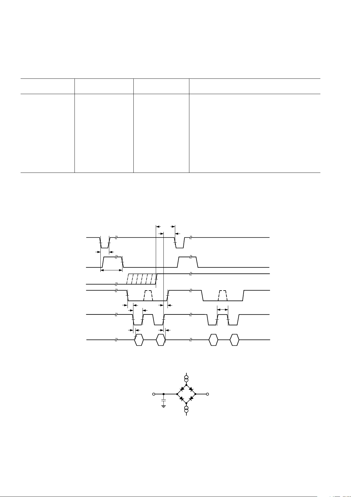
TIMING CHARACTERISTICS
1, 2
A, B
Parameter Versions Units Test Conditions/Comments
t
CONV
5.2 µs max Conversion Time
t
ACQ
0.5 µs max Acquisition Time
Parallel Interface
t
1
0 ns min CS to RD Setup Time
t
2
0 ns min CS to RD Hold Time
t
3
35 ns min CONVST Pulsewidth
t
4
45 ns min Read Pulsewidth
t
5
3
30 ns min Data Access Time after Falling Edge of RD
t
6
4
5 ns min Bus Relinquish Time after Rising Edge of RD
30 ns max
t
7
10 ns min Time Between Consecutive Reads
t
8
400 ns min Quiet Time
NOTES
1
Sample tested at +25°C to ensure compliance. All input signals are measured with tr = tf = 1 ns (10% to 90% of +5 V) and timed from a voltage level of +1.6 V.
2
See Figure 1.
3
Measured with the load circuit of Figure 2 and defined as the time required for an output to cross 0.8 V or 2.0 V.
4
These times are derived from the measured time taken by the data outputs to change 0.5 V when loaded with the circuit of Figure 2. The measured number is then
extrapolated back to remove the effects of charging or discharging the 50 pF capacitor. This means that the times quoted in the timing characteristics are the true bus
relinquish times of the part and as such are independent of external bus loading capacitances.
Specifications subject to change without notice.
(VDD = +5 V 5%, AGND = DGND = 0 V, REF = Internal. All specifications T
MIN
to T
MAX
unless
otherwise noted.)
t
3
t
1
t
4
t
5
t
2
t
6
V
A1
V
A2
V
B1
V
B2
CONVST
BUSY
A0
CS
RD
DATA
t
7
t
CONV
= 5.2s
t
ACQ
t
8
Figure 1. Timing Diagram
TO OUTPUT
PIN
1.6mA
200A
50pF
Figure 2. Load Circuit for Access Time and Bus Relinquish Time

AD7863
–5–REV. A
ABSOLUTE MAXIMUM RATINGS*
(TA = +25°C unless otherwise noted)
VDD to AGND . . . . . . . . . . . . . . . . . . . . . . . . . –0.3 V to +7 V
V
DD
to DGND . . . . . . . . . . . . . . . . . . . . . . . . . –0.3 V to +7 V
Analog Input Voltage to AGND
AD7863-10 . . . . . . . . . . . . . . . . . . . . . . . . . . . . . . . . ± 17 V
AD7863-3 . . . . . . . . . . . . . . . . . . . . . . . . . . . . . . . . . . ± 7V
AD7863-2 . . . . . . . . . . . . . . . . . . . . . . . . . . . . . . . . . . +7 V
Reference Input Voltage to AGND . . . .–0.3 V to V
DD
+ 0.3 V
Digital Input Voltage to DGND . . . . . –0.3 V to V
DD
+ 0.3 V
Digital Output Voltage to DGND . . . . –0.3 V to V
DD
+ 0.3 V
Operating Temperature Range
Commercial (A, B Version) . . . . . . . . . . . . –40°C to +85°C
Storage Temperature Range . . . . . . . . . . . –65°C to +150°C
Junction Temperature . . . . . . . . . . . . . . . . . . . . . . . . . +150°C
SOIC Package, Power Dissipation . . . . . . . . . . . . . . . 450 mW
θJA Thermal Impedance . . . . . . . . . . . . . . . . . . . . 110°C/W
Lead Temperature, Soldering
Vapor Phase (60 sec) . . . . . . . . . . . . . . . . . . . . . .+215°C
Infrared (15 sec) . . . . . . . . . . . . . . . . . . . . . . . . .+220°C
SSOP Package, Power Dissipation . . . . . . . . . . . . . . . 450 mW
θ
JA
Thermal Impedance . . . . . . . . . . . . . . . . . . . . 110°C/W
Lead Temperature, Soldering
Vapor Phase (60 sec) . . . . . . . . . . . . . . . . . . . . . .+215°C
Infrared (15 sec) . . . . . . . . . . . . . . . . . . . . . . . . .+220°C
*Stresses above those listed under Absolute Maximum Ratings may cause perma-
nent damage to the device. This is a stress rating only; functional operation of the
device at these or any other conditions above those listed in the operational
sections of this specification is not implied. Exposure to absolute maximum rating
conditions for extended periods may affect device reliability.
CAUTION
ESD (electrostatic discharge) sensitive device. Electrostatic charges as high as 4000 V readily
accumulate on the human body and test equipment and can discharge without detection.
Although the AD7863 features proprietary ESD protection circuitry, permanent damage may
occur on devices subjected to high energy electrostatic discharges. Therefore, proper ESD
precautions are recommended to avoid performance degradation or loss of functionality.
ORDERING GUIDE
Model Input Ranges Relative Accuracy Temperature Range Package Options*
AD7863AR-10 ± 10 V ± 2.5 LSB –40°C to +85°C R-28
AD7863BR-10 ± 10 V ± 2.0 LSB –40°C to +85°C R-28
AD7863ARS-10 ± 10 V ± 2.5 LSB –40°C to +85°C RS-28
AD7863AR-3 ± 2.5 V ±2.5 LSB –40°C to +85°C R-28
AD7863ARS-3 ±2.5 V ± 2.5 LSB –40°C to +85°C RS-28
AD7863BR-3 ± 2.5 V ±2.0 LSB –40°C to +85°C R-28
AD7863AR-2 0 V to 2.5 V ±2.5 LSB –40°C to +85°C R-28
AD7863ARS-2 0 V to 2.5 V ± 2.5 LSB –40°C to +85°C RS-28
*R = Small Outline (SOIC), RS = Shrink Small Outline (SSOP).
WARNING!
ESD SENSITIVE DEVICE
AD7863
–6–
REV. A
PIN FUNCTION DESCRIPTIONS
Pin Mnemonic Description
1–6 DB12–DB7 Data Bit 12 to Data Bit 7. Three-state TTL outputs.
7 DGND Digital Ground. Ground reference for digital circuitry.
8 CONVST Convert Start Input. Logic Input. A high to low transition on this input puts both track/holds into their hold
mode and starts conversion on both channels.
9–15 DB6–DB0 Data Bit 6 to Data Bit 0. Three-state TTL outputs.
16 AGND Analog Ground. Ground reference for Mux, track/hold, reference and DAC circuitry.
17 V
B2
Input Number 2 of Channel B. Analog Input voltage ranges of ±10 V (AD7863-10), ± 2.5 V (AD7863-3)
and 0 V–2.5 V (AD7863-2).
18 V
A2
Input Number 2 of Channel A. Analog Input voltage ranges of ±10 V (AD7863-10), ±2.5 V (AD7863-3)
and 0 V–2.5 V (AD7863-2).
19 V
REF
Reference Input/Output. This pin is connected to the internal reference through a series resistor and is the
output reference source for the analog-to-digital converter. The nominal reference voltage is 2.5 V and this
appears at the pin.
20 A0 Multiplexer Select. This input is used in conjunction with CONVST to determine on which pair of channels
the conversion is to be performed. If A0 is low when the conversion is initiated then channels V
A1, VA2
will
be selected. If A0 is high when the conversion is initiated, channels V
B1, VB2
will be selected.
21 CS Chip Select Input. Active low logic input. The device is selected when this input is active.
22 RD Read Input. Active low logic input. This input is used in conjunction with CS low to enable the data out-
puts and read a conversion result from the AD7863.
23 BUSY Busy Output. The busy output is triggered high by the falling edge of CONVST and remains high until
conversion is completed.
24 V
DD
Analog and Digital Positive Supply Voltage, +5.0 V ± 5%.
25 V
A1
Input Number 1 of Channel A. Analog Input voltage ranges of ±10 V (AD7863-10), ±2.5 V (AD7863-3)
and 0 V–2.5 V (AD7863-2).
26 V
B1
Input Number 1 of Channel B. Analog Input voltage ranges of ±10 V (AD7863-10), ± 2.5 V (AD7863-3)
and 0 V–2.5 V (AD7863-2).
27 AGND Analog Ground. Ground reference for Mux, track/hold, reference and DAC circuitry.
28 DB13 Data Bit 13 (MSB). Three-state TTL output. Output coding is twos complement for the AD7863-10 and
AD7863-3. Output coding is straight (natural) binary for the AD7863-2.
PIN CONFIGURATION
TOP VIEW
(Not to Scale)
28
27
26
25
24
23
22
21
20
19
18
17
16
15
1
2
3
4
5
6
7
8
9
10
11
12
13
14
AD7863
DB1
DB2
DB3
DB4
DB5
DB6
CONVST
DB12
DB11
DB10
DB9
DGND
DB7
DB8
V
A2
V
REF
A0
CS
DB13
AGND
V
B1
V
A1
RD
BUSY
V
DD
V
B2
AGND
DB0

AD7863
–7–REV. A
TERMINOLOGY
Signal to (Noise + Distortion) Ratio
This is the measured ratio of signal to (noise + distortion) at the
output of the A/D converter. The signal is the rms amplitude of
the fundamental. Noise is the rms sum of all nonfundamental
signals up to half the sampling frequency (f
S
/2), excluding dc.
The ratio is dependent upon the number of quantization levels
in the digitization process; the more levels, the smaller the quantization noise. The theoretical signal to (noise + distortion) ratio
for an ideal N-bit converter with a sine wave input is given by:
Signal to (Noise + Distortion) = (6.02N + 1.76) dB
Thus for a 14-bit converter, this is 86.04 dB.
Total Harmonic Distortion
Total harmonic distortion (THD) is the ratio of the rms sum of
harmonics to the fundamental. For the AD7863 it is defined as:
THD (dB) = 20 log
V
2
2
+V
3
2
+V
4
2
+V
5
2
V
1
where V1 is the rms amplitude of the fundamental and V2, V3,
V
4
and V5 are the rms amplitudes of the second through the
fifth harmonics.
Peak Harmonic or Spurious Noise
Peak harmonic or spurious noise is defined as the ratio of the
rms value of the next largest component in the ADC output
spectrum (up to f
S
/2 and excluding dc) to the rms value of the
fundamental. Normally, the value of this specification is determined by the largest harmonic in the spectrum, but for parts
where the harmonics are buried in the noise floor, it will be a
noise peak.
Intermodulation Distortion
With inputs consisting of sine waves at two frequencies, fa and
fb, any active device with nonlinearities will create distortion
products at sum and difference frequencies of mfa ± nfb where
m, n = 0, 1, 2, 3, etc. Intermodulation terms are those for
which neither m nor n are equal to zero. For example, the
second order terms include (fa + fb) and (fa – fb), while the
third order terms include (2fa + fb), (2fa – fb), (fa + 2fb)
and (fa – 2fb).
The AD7863 is tested using two input frequencies. In this case,
the second and third order terms are of different significance.
The second order terms are usually distanced in frequency from
the original sine waves, while the third order terms are usually at
a frequency close to the input frequencies. As a result, the
second and third order terms are specified separately. The
calculation of the intermodulation distortion is as per the THD
specification where it is the ratio of the rms sum of the individual distortion products to the rms amplitude of the fundamental expressed in dBs.
Channel-to-Channel Isolation
Channel-to-Channel isolation is a measure of the level of
crosstalk between channels. It is measured by applying a fullscale 50 kHz sine wave signal to all nonselected channels and
determining how much that signal is attenuated in the selected
channel. The figure given is the worst case across all channels.
Relative Accuracy
Relative accuracy or endpoint nonlinearity is the maximum
deviation from a straight line passing through the endpoints of
the ADC transfer function.
Differential Nonlinearity
This is the difference between the measured and the ideal
1 LSB change between any two adjacent codes in the ADC.
Positive Gain Error (AD7863-10, 10 V, AD7863-3, 2.5 V)
This is the deviation of the last code transition (01 . . . 110 to
01 . . . 111) from the ideal 4 × V
REF
– 1 LSB (AD7863-10
± 10 V range) or V
REF
– 1 LSB (AD7863-3, ± 2.5 V range), after
the Bipolar Offset Error has been adjusted out.
Positive Gain Error (AD7863-2, 0 V to 2.5 V)
This is the deviation of the last code transition (11 . . . 110 to
11 . . . 111) from the ideal V
REF
– 1 LSB, after the unipolar
offset error has been adjusted out.
Bipolar Zero Error (AD7863-10, 10 V, AD7863-3, 2.5 V)
This is the deviation of the midscale transition (all 0s to all 1s)
from the ideal 0 V (AGND).
Unipolar Offset Error (AD7863-2, 0 V to 2.5 V)
This is the deviation of the first code transition (00 . . . 000 to
00 . . . 001) from the ideal AGND + 1 LSB.
Negative Gain Error (AD7863-10, 10 V, AD7863-3, 2.5 V)
This is the deviation of the first code transition (10 . . . 000 to
10 . . . 001) from the ideal –4 × V
REF
+ 1 LSB (AD7863-10
± 10 V range) or –V
REF
+ 1 LSB (AD7863-3, ±2.5 V range),
after Bipolar Zero Error has been adjusted out.
Track/Hold Acquisition Time
Track/hold acquisition time is the time required for the output
of the track/hold amplifier to reach its final value, within
± 1/2 LSB, after the end of conversion (the point at which the
track/hold returns to track mode). It also applies to situations
where a change in the selected input channel takes place or
where there is a step input change on the input voltage applied
to the selected V
AX/BX
input of the AD7863. It means that the
user must wait for the duration of the track/hold acquisition
time after the end of conversion or after a channel change/step
input change to V
AX/BX
before starting another conversion, to
ensure that the part operates to specification.

AD7863
–8–
REV. A
CONVERTER DETAILS
The AD7863 is a high speed, low power, dual 14-bit A/D converter that operates from a single +5 V supply. The part contains two 5.2 µs successive approximation ADCs, two track/
hold amplifiers, an internal +2.5 V reference and a high speed
parallel interface. Four analog inputs are grouped into two
channels (A and B) selected by the A0 input. Each channel has
two inputs (V
A1
and VA2 or VB1 and VB2) which can be sampled
and converted simultaneously thus preserving the relative phase
information of the signals on both analog inputs. The part
accepts an analog input range of ±10 V (AD7863-10), ±2.5 V
(AD7863-3) and 0 V–2.5 V (AD7863-2). Overvoltage protection on the analog inputs for the part allows the input voltage to
go to ± 17 V, ± 7 V or +7 V respectively, without causing damage. The AD7863 has two operating modes, the high sampling
mode and the auto sleep mode where the part automatically
goes into sleep after the end of conversion. These modes are
discussed in more detail in the Timing and Control section.
Conversion is initiated on the AD7863 by pulsing the CONVST
input. On the falling edge of CONVST, both on-chip track/
holds are simultaneously placed into hold and the conversion
sequence is started on both channels. The conversion clock for
the part is generated internally using a laser-trimmed clock
oscillator circuit. The BUSY signal indicates the end of conversion and at this time the conversion results for both channels
are available to be read. The first read after a conversion accesses the result from V
A1
or VB1, while the second read ac-
cesses the result from V
A2
or VB2 depending on whether the
multiplexer select A0 is low or high respectively before the
conversion is initiated. Data is read from the part via a 14-bit
parallel data bus with standard CS and RD signals.
Conversion time for the AD7863 is 5.2 µs in the high sampling
mode (10 µs for the auto sleep mode), and the track/hold acqui-
sition time is 0.5 µs. To obtain optimum performance from the
part, the read operation should not occur during the conversion
or during the 400 ns prior to the next conversion. This allows
the part to operate at throughput rates up to 175 kHz and
achieve data sheet specifications.
Track/Hold Section
The track/hold amplifiers on the AD7863 allow the ADCs to
accurately convert an input sine wave of full-scale amplitude to
14-bit accuracy. The input bandwidth of the track/hold is
greater than the Nyquist rate of the ADC, even when the ADC
is operated at its maximum throughput rate of 175 kHz (i.e.,
the track/hold can handle input frequencies in excess of 87.5 kHz).
The track/hold amplifiers acquire input signals to 14-bit accuracy in less than 500 ns. The operation of the track/holds are
essentially transparent to the user. The two track/hold amplifiers sample their respective input channels simultaneously, on
the falling edge of CONVST. The aperture time for the track/
holds (i.e., the delay time between the external CONVST signal
and the track/hold actually going into hold) is well matched
across the two track/holds on one device and also well matched
from device to device. This allows the relative phase information
between different input channels to be accurately preserved. It
also allows multiple AD7863s to simultaneously sample more
than two channels. At the end of conversion, the part returns to
its tracking mode. The acquisition time of the track/hold amplifiers begins at this point.
Reference Section
The AD7863 contains a single reference pin, labeled V
REF
,
which either provides access to the part’s own +2.5 V reference
or to which an external +2.5 V reference can be connected to
provide the reference source for the part. The part is specified
with a +2.5 V reference voltage. Errors in the reference source
will result in gain errors in the AD7863’s transfer function and
will add to the specified full-scale errors on the part. On the
AD7863-10 and AD7863-3, it will also result in an offset error
injected in the attenuator stage.
The AD7863 contains an on-chip +2.5 V reference. To use this
reference as the reference source for the AD7863, simply
connect two 0.1 µF disc ceramic capacitors from the V
REF
pin
to AGND. The voltage that appears at this pin is internally
buffered before being applied to the ADC. If this reference is
required for use external to the AD7863, it should be buffered
as the part has a FET switch in series with the reference output
resulting in a source impedance for this output of 5.5 kΩ nominal. The tolerance on the internal reference is ±10 mV at 25°C
with a typical temperature coefficient of 25 ppm/°C and a maximum error over temperature of ±25 mV.
If the application requires a reference with a tighter tolerance or
the AD7863 needs to be used with a system reference, the user
has the option of connecting an external reference to this V
REF
pin. The external reference will effectively overdrive the internal
reference and thus provide the reference source for the ADC.
The reference input is buffered before being applied to the
ADC with a maximum input current of ±100 µA. A suitable
reference source for the AD7863 is the AD780 precision
+2.5 V reference.

AD7863
–9–REV. A
CIRCUIT DESCRIPTION
Analog Input Section
The AD7863 is offered as three part types: the AD7863-10,
which handles a ±10 V input voltage range, the AD7863-3,
which handles input voltage range ±2.5 V and the AD7863-2,
which handles a 0 V to +2.5 V input voltage range.
2k
+2.5V
REFERENCE
MUX
R2
R1
R3
TO ADC
REFERENCE
CIRCUITRY
TO INTERNAL
COMPARATOR
TRACK/
HOLD
V
REF
V
AX
AGND
AD7863-10/AD7863-3
Figure 3. AD7863-10/-3 Analog Input Structure
Figure 3 shows the analog input section for the AD7863-10 and
AD7863-3. The analog input range of the AD7863-10 is ±10 V
into an input resistance of typically 9 kΩ. The analog input
range of the AD7863-3 is ±2.5 V into an input resistance of
typically 3 kΩ. This input is benign, with no dynamic charging
currents as the resistor stage is followed by a high input impedance stage of the track/hold amplifier. For the AD7863-10, R1
= 8 kΩ, R2 = 2 kΩ and R3 = 2 kΩ. For the AD7863-3, R1 = R2
= 2 kΩ and R3 is open circuit.
For the AD7863-10 and AD7863-3, the designed code transitions occur on successive integer LSB values (i.e., 1 LSB, 2 LSBs,
3 LSBs . . .). Output coding is twos complement binary with
1 LSB = FS/16384. The ideal input/output transfer function for
the AD7863-10 and AD7863-3 is shown in Table I.
Table I. Ideal Input/Output Code Table for the AD7863-10/-3
Digital Output
Analog Input
l
Code Transition
+FSR/2 – 1 LSB
2
011 . . . 110 to 011 . . . 111
+FSR/2 – 2 LSBs 011 . . . 101 to 011 . . . 110
+FSR/2 – 3 LSBs 011 . . . 100 to 011 . . . 101
GND + 1 LSB 000 . . . 000 to 000 . . . 001
GND 111 . . . 111 to 000 . . . 000
GND – 1 LSB 111 . . . 110 to 111 . . . 111
–FSR/2 + 3 LSBs 100 . . . 010 to 100 . . . 011
–FSR/2 + 2 LSBs 100 . . . 001 to 100 . . . 010
–FSR/2 + 1 LSB 100 . . . 000 to 100 . . . 001
NOTES
1
FSR is full-scale range = 20 V (AD7863-10) and = 5 V (AD7863-3) with
REF IN = +2.5 V.
2
1 LSB = FSR/16384 = 1.22 mV (AD7863-10) and 0.3 mV (AD7863-3) with
REF IN = +2.5 V.
The analog input section for the AD7863-2 contains no biasing
resistors and the V
AX/BX
pin drives the input directly to the
multiplexer and track/hold amplifier circuitry. The analog input
range is 0 V to +2.5 V into a high impedance stage with an
input current of less than 100 nA. This input is benign, with no
dynamic charging currents. Once again, the designed code transitions occur on successive integer LSB values. Output coding is
straight (natural) binary with 1 LSB = FS/16384 = 2.5 V/16384
= 0.15 mV. Table II shows the ideal input/output transfer function for the AD7863-2.
Table II. Ideal Input/Output Code Table for the AD7863-2
Digital Output
Analog Input
1
Code Transition
+FSR – 1 LSB
2
111 . . . 110 to 111 . . . 111
+FSR – 2 LSB 111 . . . 101 to 111 . . . 110
+FSR – 3 LSB 111 . . . 100 to 111 . . . 101
GND + 3 LSB 000 . . . 010 to 000 . . . 011
GND + 2 LSB 000 . . . 001 to 000 . . . 010
GND + 1 LSB 000 . . . 000 to 000 . . . 001
NOTES
1
FSR is Full-Scale Range and is 2.5 V for AD7863-2 with V
REF
= +2.5 V.
2
1 LSB = FSR/16384 and is 0.15 mV for AD7863-2 with V
REF
= +2.5 V.
OFFSET AND FULL-SCALE ADJUSTMENT
In most Digital Signal Processing (DSP) applications, offset and
full-scale errors have little or no effect on system performance.
Offset error can always be eliminated in the analog domain by
ac coupling. Full-scale error effect is linear and does not cause
problems as long as the input signal is within the full dynamic
range of the ADC. Invariably, some applications will require
that the input signal span the full analog input dynamic range.
In such applications, offset and full-scale error will have to be
adjusted to zero.
Figure 4 shows a typical circuit that can be used to adjust the
offset and full-scale errors on the AD7863 (VA1 on the AD786310 version is shown for example purposes only). Where adjustment is required, offset error must be adjusted before full-scale
error. This is achieved by trimming the offset of the op amp
driving the analog input of the AD7863 while the input voltage is
1/2 LSB below analog ground. The trim procedure is as follows:
apply a voltage of –0.61 mV (–1/2 LSB) at V
1
in Figure 4 and
adjust the op amp offset voltage until the ADC output code
flickers between 11 1111 1111 1111 and 00 0000 0000 0000.
R2
500
*ADDITIONAL PINS OMITTED FOR CLARITY
V
A1
AGND
AD7863*
R1
10k
R4
10k
R5
10k
R3
10k
V
1
INPUT RANGE = 10V
Figure 4. Full-Scale Adjust Circuit

AD7863
–10–
REV. A
Gain error can be adjusted at either the first code transition (ADC
negative full scale) or the last code transition (ADC positive full
scale). The trim procedures for both cases are as follows:
Positive Full-Scale Adjust (-10 Version)
Apply a voltage of +9.9927 V (FS/2 – 1 LSBs) at V1. Adjust R2
until the ADC output code flickers between 01 1111 1111 1110
and 01 1111 1111 1111.
Negative Full-Scale Adjust (-10 Version)
Apply a voltage of –9.9976 V (–FS + 1 LSB) at V1 and adjust
R2 until the ADC output code flickers between 10 0000 0000
0000 and 10 0000 0000 0001.
An alternative scheme for adjusting full-scale error in systems
that use an external reference is to adjust the voltage at the V
REF
pin until the full-scale error for any of the channels is adjusted
out. The good full-scale matching of the channels will ensure
small full-scale errors on the other channels.
TIMING AND CONTROL
Figure 5a shows the timing and control sequence required to
obtain optimum performance (Mode 1) from the AD7863. In
the sequence shown, a conversion is initiated on the falling edge
of CONVST. This places both track/holds into hold simultaneously and new data from this conversion is available in the
output register of the AD7863 5.2 µs later. The BUSY signal
indicates the end of conversion and at this time the conversion
results for both channels are available to be read. A second
conversion is then initiated. If the multiplexer select A0 is low,
the first and second read pulses after the first conversion accesses the result from Channel A (V
A1
and VA2 respectively).
The third and fourth read pulses, after the second conversion
and A0 high, accesses the result from Channel B (V
B1
and V
B2
respectively). A0’s state can be changed any time after the
CONVST goes high, i.e., track/holds into hold and 500 ns prior
to the next falling edge of CONVST. Note that A0 should not
be changed during conversion if the nonselected channels have
negative voltages applied to them which are outside the input
range of the AD7863, as this will affect the conversion in
progress. Data is read from the part via a 14-bit parallel data bus
with standard CS and RD signal, i.e., the read operation consists of a negative going pulse on the CS pin combined with two
negative going pulses on the RD pin (while the CS is low),
accessing the two 14-bit results. Once the read operation has
taken place, a further 400 ns should be allowed before the next
falling edge of CONVST to optimize the settling of the track/
hold amplifier before the next conversion is initiated. The
achievable throughput rate for the part is 5.2 µs (conversion
time) plus 100 ns (read time) plus 0.4 µs (quiet time). This
results in a minimum throughput time of 5.7 µs (equivalent to a
throughput rate of 175 kHz).
Read Options
Apart from the Read Operation described above and displayed
in Figure 5a, other CS and RD combinations can result in different channels/inputs being read in different combinations.
Suitable combinations are shown in Figures 5b through 5d.
CS
RD
DATA
V
A1
V
A2
Figure 5b. Read Option A (A0 Is Low)
CS
RD
DATA
V
A1
V
A2
V
A1
Figure 5c. Read Option B (A0 Is Low)
t
3
t
5
t
4
V
A1
V
A2
V
B1
V
B2
CONVST
BUSY
A0
CS
RD
DATA
t
1
t
7
t
2
t
6
t
CONV
= 5.2s
t
ACQ
t
8
Figure 5a. Mode 1 Timing Operation Diagram for High Sampling Performance

AD7863
–11–REV. A
CS
RD
DATA
V
A1
V
A2
A0
Figure 5d. Read Option C
OPERATING MODES
Mode 1 Operation (Normal Power, High Sampling
Performance)
The timing diagram in Figure 5a is for optimum performance in
operating Mode 1 where the falling edge of CONVST starts
conversion and puts the track/hold amplifiers into their hold
mode. This falling edge of CONVST also causes the BUSY
signal to go high to indicate that a conversion is taking place.
The BUSY signal goes low when the conversion is complete,
which is 5.2 µs max after the falling edge of CONVST and new
data from this conversion is available in the output latch of the
AD7863. A read operation accesses this data. If the multiplexer
select A0 is low, the first and second read pulses after the first
conversion accesses the result from Channel A (V
A1
and V
A2
respectively). The third and fourth read pulses, after the second
conversion and A0 high, access the result from Channel B (V
B1
and VB2, respectively). Data is read from the part via a 14-bit
parallel data bus with standard CS and RD signals. This data
read operation consists of a negative going pulse on the CS pin
combined with two negative going pulses on the RD pin (while
the CS is low), accessing the two 14-bit results. For the fastest
throughput rate the read operation will take 100 ns. The read
operation must be complete at least 400 ns before the falling
edge of the next CONVST and this gives a total time of 5.7 µs
for the full throughput time (equivalent to 175 kHz). This mode of
operation should be used for high sampling applications.
Mode 2 Operation (Power-Down, Auto-Sleep After
Conversion)
The timing diagram in Figure 6 is for optimum performance in
operating Mode 2 where the part automatically goes into sleep
mode once BUSY goes low after conversion and “wakes up”
before the next conversion takes place. This is achieved by keeping CONVST low at the end of the second conversion, whereas
it was high at the end of the second conversion for Mode 1
operation.
The operation shown in Figure 6 shows how to access data from
both Channels A and B, followed by the Auto Sleep mode. One
can also set up the timing to access data from Channel A only or
Channel B only (see Read Options section) and then go into
Auto-Sleep mode. The rising edge of CONVST “wakes up” the
part. This wake-up time is 4.8 µs when using an external refer-
ence and 5 ms when using the internal reference, at which point
the track/hold amplifiers go into their hold mode provided the
CONVST has gone low. The conversion takes 5.2 µs after this
giving a total of 10 µs (external reference, 5.005 ms for internal
reference) from the rising edge of CONVST to the conversion
being complete, which is indicated by the BUSY going low.
Note that since the wake-up time from the rising edge of CONVST
is 4.8 µs, if the CONVST pulsewidth is greater than 5.2 µs the
conversion will take more than the 10 µs (4.8 µs wake-up time
+5.2 µs conversion time) shown in Figure 6 from the rising edge
of CONVST. This is because the track/hold amplifiers go into
their hold mode on the falling edge of CONVST and the conversion will not be complete for a further 5.2 µs. In this case, the
BUSY will be the best indicator of when the conversion is complete. Even though the part is in sleep mode, data can still be
read from the part.
The read operation is identical to that in Mode 1 operation and
must also be complete at least 400 ns before the falling edge of
the next CONVST to allow the track/hold amplifiers to have
enough time to settle. This mode is very useful when the part is
converting at a slow rate as the power consumption will be
significantly reduced from that of Mode 1 operation.
t
3
t
CONV
= 5.2s
V
A1
V
A2
V
B1
V
B2
CONVST
BUSY
A0
CS
RD
DATA
t
3
4.8s*/5ms**
WAKE-UP TIME
t
CONV
= 5.2s
* WHEN USING AN EXTERNAL REFERENCE, WAKE-UP TIME = 4.8s
** WHEN USING AN INTERNAL REFERENCE, WAKE-UP TIME = 5ms
t
ACQ
t
8
Figure 6. Mode 2 Timing Diagram Where Automatic Sleep Function Is Initiated
AD7863
–12–
REV. A
AD7863 DYNAMIC SPECIFICATIONS
The AD7863 is specified and tested for dynamic performance
specifications as well as traditional dc specifications such as
Integral and Differential Nonlinearity. These ac specifications
are required for the signal processing applications such as
phased array sonar, adaptive filters and spectrum analysis.
These applications require information on the ADC’s effect on
the spectral content of the input signal. Hence, the parameters
for which the AD7863 is specified include SNR, harmonic distortion, intermodulation distortion and peak harmonics. These
terms are discussed in more detail in the following sections.
Signal-to-Noise Ratio (SNR)
SNR is the measured signal to noise ratio at the output of the
ADC. The signal is the rms magnitude of the fundamental.
Noise is the rms sum of all the nonfundamental signals up to
half the sampling frequency (f
S
/2), excluding dc. SNR is dependent upon the number of quantization levels used in the digitization process; the more levels, the smaller the quantization
noise. The theoretical signal to noise ratio for a sine wave input
is given by
SNR = (6.02N + 1.76) dB (1)
where N is the number of bits.
Thus for an ideal 14-bit converter, SNR = 86.04 dB.
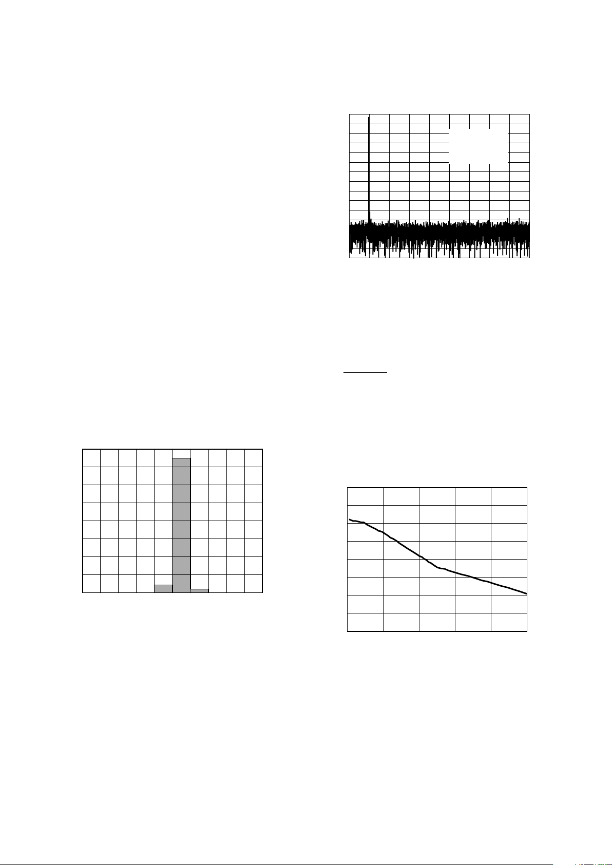
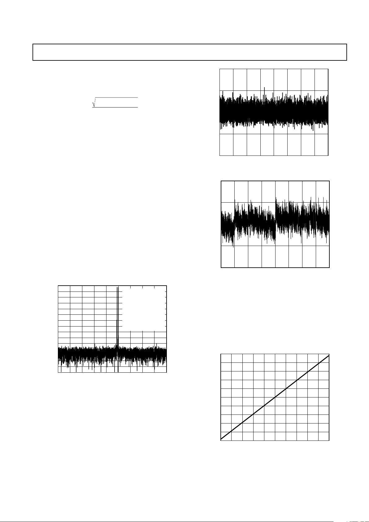
Figure 7 shows a histogram plot for 8,192 conversions of a dc
input using the AD7863 with 5 V supply. The analog input was
set at the center of a code transition. It can be seen that the
codes appear mainly in the one output bin, indicating very good
noise performance from the ADC.
CODE
8000
746
COUNTS
7000
6000
5000
4000
3000
2000
1000
0
747 748 749 750 751 752 753 754 755
Figure 7. Histogram of 8,192 Conversions of a DC Input
The output spectrum from the ADC is evaluated by applying a
sine wave signal of very low distortion to the V
AX/BX
input,
which is sampled at a 175 kHz sampling rate. A Fast Fourier
Transform (FFT) plot is generated from which the SNR data
can be obtained. Figure 8 shows a typical 8,192 point FFT plot
of the AD7863 with an input signal of 10 kHz and a sampling
frequency of 175 kHz. The SNR obtained from this graph is
–80.72 dB. It should be noted that the harmonics are taken into
account when calculating the SNR.
FREQUENCY – kHz
0
–130
10
dB
–120
–110
–100
–90
–80
–70
–60
–50
–40
–30
–20
–10
20 30 40 50 60 70 80 90
F
SAMPLE
= 175kHz
F
IN
= 10kHz
SNR = +80.72dB
THD = –92.96dB
–140
–150
Figure 8. AD7863 FFT Plot
Effective Number of Bits
The formula given in Equation 1 relates the SNR to the number
of bits. Rewriting the formula, as in Equation 2, it is possible to
obtain a measure of performance expressed in effective number
of bits (N).
N =
SNR – 1. 7 6
6.02
(2)
The effective number of bits for a device can be calculated directly from its measured SNR.
Figure 9 shows a typical plot of effective number of bits versus
frequency for an AD7863-2 with a sampling frequency of
175 kHz. The effective number of bits typically falls between
13.11 and 11.05 corresponding to SNR figures of +80.68 dB
and +68.28 dB.
FREQUENCY – kHz
14.0
0
1000200
ENOB
400 600 800
13.5
13.0
12.5
12.0
11.5
11.0
10.5
10.0
Figure 9. Effective Numbers of Bits vs. Frequency
AD7863
–13–REV. A
Total Harmonic Distortion (THD)
Total Harmonic Distortion (THD) is the ratio of the rms sum
of harmonics to the rms value of the fundamental. For the
AD7863, THD is defined as
THD (dB) = 20 log
V
2
2
+V
3
2
+V
4
2
+V
5
2
V
1
where V1 is the rms amplitude of the fundamental and V2, V3,
V
4
and V5 are the rms amplitudes of the second through the
sixth harmonic. The THD is also derived from the FFT plot of
the ADC output spectrum.
Intermodulation Distortion
With inputs consisting of sine waves at two frequencies, fa and
fb, any active device with nonlinearities will create distortion
products at sum and difference frequencies of mfa ± nfb where
m, n = 0, 1, 2, 3 . . ., etc. Intermodulation terms are those for
which neither m nor n are equal to zero. For example, the second
order terms include (fa + fb) and (fa – fb) while the third order
terms include (2fa + fb), (2fa – fb), (fa + 2fb) and (fa – 2fb).
In this case, the second and third order terms are of different
significance. The second order terms are usually distanced in
frequency from the original sine waves while the third order
terms are usually at a frequency close to the input frequencies.
As a result, the second and third order terms are specified separately. The calculation of the intermodulation distortion is as
per the THD specification where it is the ratio of the rms sum
of the individual distortion products to the rms amplitude of the
fundamental expressed in dBs. In this case, the input consists of
two equal amplitude, low distortion sine waves. Figure 10 shows
a typical IMD plot for the AD7863.
FREQUENCY – kHz
0
–130
10
dB
–120
–110
–100
–90
–80
–70
–60
–50
–40
–30
–20
–10
20 30 40 50 60 70 80
INPUT FREQUENCIES
F1 = 50.13kHz
F2 = 49.13kHz
F
SAMPLE
= 175kHz
IMD:
2ND ORDER TERM
–98.21dB
3RD ORDER TERM
–93.91dB
–140
–150
0
90
Figure 10. IMD Plot
Peak Harmonic or Spurious Noise
Harmonic or Spurious Noise is defined as the ratio of the rms
value of the next largest component in the ADC output spectrum (up to f
S
/2 and excluding dc) to the rms value of the fundamental. Normally, the value of this specification will be
determined by the largest harmonic in the spectrum, but for
parts where the harmonics are buried in the noise floor the peak
will be a noise peak.
DC Linearity Plot
Figures 11 and 12 show typical DNL and INL plots for the
AD7863.
1
0
–1
DNL ERROR – LSB
–0.5
0.5
0 2048 4096 6144 8192 10240 12288 14336 16383
ADC CODE
Figure 11. DC DNL Plot
1
0
–1
INL ERROR – LSB
–0.5
0.5
0 2048 4096 6144 8192 10240 12288 14336 16383
ADC CODE
Figure 12. DC INL Plot
Power Considerations
In the automatic power-down mode then the part may be operated at a sample rate that is considerably less than 175 kHz. In
this case, the power consumption will be reduced and will depend on the sample rate. Figure 13 shows a graph of the power
consumption versus sampling rates from 1 Hz to 100 kHz in the
automatic power-down mode. The conditions are 5 V supply
25°C.
FREQUENCY – kHz
50
0
0
POWER – mW
45
40
35
30
25
20
15
10
5
10 20 30 40 50 60 70 80 90 100
Figure 13. Power vs. Sample Rate in Auto Power-Down
Mode

AD7863
–14–
REV. A
MICROPROCESSOR INTERFACING
The AD7863 high speed bus timing allows direct interfacing to
DSP processors as well as modern 16-bit microprocessors.
Suitable microprocessor interfaces are shown in Figures 14
through 18.
AD7863–ADSP-2100 Interface
Figure 14 shows an interface between the AD7863 and the
ADSP-2100. The CONVST signal can be supplied from the
ADSP-2100 or from an external source. The AD7863 BUSY
line provides an interrupt to the ADSP-2100 when conversion is
completed on both channels. The two conversion results can
then be read from the AD7863 using two successive reads to the
same memory address. The following instruction reads one of
the two results:
MR0 = DM (ADC)
where MR0 is the ADSP-2100 MR0 register and ADC is the
AD7863 address.
ADDR
DECODE
EN
ADDRESS BUS
DMA13
DMA0
DMS
IRQn
DMRD (RD)
DMD15
DMD0
CS
A0
BUSY
RD
DB13
DB0
DATA BUS
ADSP-2100
(ADSP-2101/
ADSP-2102)
AD7863*
*ADDITIONAL PINS OMITTED FOR CLARITY
OPTIONAL
CONVST
Figure 14. AD7863–ADSP-2100 Interface
AD7863–ADSP-2101/ADSP-2102 Interface
The interface outlined in Figure 14 also forms the basis for an
interface between the AD7863 and the ADSP-2101/ADSP-2102.
The READ line of the ADSP-2101/ADSP-2102 is labeled RD.
In this interface, the RD pulsewidth of the processor can be
programmed using the Data Memory Wait State Control Register. The instruction used to read one of the two results is as
outlined for the ADSP-2100.
AD7863–TMS32010 Interface
An interface between the AD7863 and the TMS32010 is
shown in Figure 15. Once again the CONVST signal can be
supplied from the TMS32010 or from an external source,
and the TMS32010 is interrupted when both conversions have
been completed. The following instruction is used to read the
conversion results from the AD7863:
IN D, ADC
where D is Data Memory address and ADC is the AD7863
address.
ADDR
DECODE
EN
ADDRESS BUS
PA2
PA0
MEN
INT
DEN
D15
D0
CS
A0
BUSY
RD
DB13
DB0
DATA BUS
TMS32010
AD7863*
*ADDITIONAL PINS OMITTED FOR CLARITY
OPTIONAL
CONVST
Figure 15. AD7863–TMS32010 Interface
AD7863–TMS320C25 Interface
Figure 16 shows an interface between the AD7863 and the
TMS320C25. As with the two previous interfaces, conversion
can be initiated from the TMS320C25 or from an external
source, and the processor is interrupted when the conversion
sequence is completed. The TMS320C25 does not have a separate RD output to drive the AD7863 RD input directly. This
has to be generated from the processor STRB and R/W outputs
with the addition of some logic gates. The RD signal is ORgated with the MSC signal to provide the one WAIT state required in the read cycle for correct interface timing. Conversion
results are read from the AD7863 using the following instruction:
IN D, ADC
where D is Data Memory address and ADC is the AD7863
address.
ADDR
DECODE
EN
ADDRESS BUS
A15
A0
IS
INTn
STRB
DMD15
DMD0
CS
A0
BUSY
RD
DB13
DB0
DATA BUS
TMS320C25
AD7863*
*ADDITIONAL PINS OMITTED FOR CLARITY
OPTIONAL
CONVST
R/ W
READY
MSC
Figure 16. AD7863–TMS320C25 Interface
Some applications may require that the conversion is initiated
by the microprocessor rather than an external timer. One option
is to decode the AD7863 CONVST from the address bus so
that a write operation starts a conversion. Data is read at the
end of the conversion sequence as before. Figure 18 shows an
example of initiating conversion using this method. Note that
for all interfaces, it is preferred that a read operation not be
attempted during conversion.

AD7863
–15–REV. A
AD7863–MC68000 Interface
An interface between the AD7863 and the MC68000 is shown
in Figure 17. As before, conversion can be supplied from the
MC68000 or from an external source. The AD7863 BUSY line
can be used to interrupt the processor or, alternatively, software
delays can ensure that conversion has been completed before a
read to the AD7863 is attempted. Because of the nature of its
interrupts, the MC68000 requires additional logic (not shown in
Figure 18) to allow it to be interrupted correctly. For further
information on MC68000 interrupts, consult the MC68000 users
manual.
The MC68000 AS and R/W outputs are used to generate a
separate RD input signal for the AD7863. CS is used to drive the
68000 DTACK input to allow the processor to execute a normal
read operation to the AD7863. The conversion results are read
using the following 68000 instruction:
MOVE.W ADC, D0
where D0 is the 68000 D0 register and ADC is the AD7863
address.
ADDR
DECODE
EN
ADDRESS BUS
A15
A0
DTACK
AS
D15
D0
CS
A0
RD
DB13
DB0
DATA BUS
MC68000
AD7863*
*ADDITIONAL PINS OMITTED FOR CLARITY
OPTIONAL
CONVST
R/ W
Figure 17. AD7863–MC68000 Interface
AD7863–80C196 Interface
Figure 18 shows an interface between the AD7863 and the
80C196 microprocessor. Here, the microprocessor initiates
conversion. This is achieved by gating the 80C196 WR signal
with a decoded address output (different from the AD7863 CS
address). The AD7863 BUSY line is used to interrupt the microprocessor when the conversion sequence is completed.
ADDR
DECODE
EN
ADDRESS BUS
A15
A1
WR
D15
D0
CS
A0
BUSY
RD
DB13
DB0
DATA BUS
80C196
AD7863*
*ADDITIONAL PINS OMITTED FOR CLARITY
RD
Figure 18. AD7863–80C196 Interface
Vector Motor Control
The current drawn by a motor can be split into two components: one produces torque and the other produces magnetic
flux. For optimal performance of the motor, these two components should be controlled independently. In conventional
methods of controlling a three-phase motor, the current (or
voltage) supplied to the motor and the frequency of the drive are
the basic control variables. However, both the torque and flux
are functions of current (or voltage) and frequency. This coupling effect can reduce the performance of the motor because,
for example, if the torque is increased by increasing the frequency, the flux tends to decrease.
Vector control of an ac motor involves controlling phase in
addition to drive and current frequency. Controlling the phase
of the motor requires feedback information on the position of
the rotor relative to the rotating magnetic field in the motor.
Using this information, a vector controller mathematically transforms the three phase drive currents into separate torque and
flux components. The AD7863 is ideally suited for use in vector
motor control applications.
A block diagram of a vector motor control application using the
AD7863 is shown in Figure 19. The position of the field is
derived by determining the current in each phase of the motor.
Only two phase currents need to be measured because the third
can be calculated if two phases are known. V
A1
and VA2 of the
AD7863 are used to digitize this information.
Simultaneous sampling is critical to maintain the relative phase
information between the two channels. A current sensing isolation amplifier, transformer or Hall effect sensor is used between
the motor and the AD7863. Rotor information is obtained by
measuring the voltage from two of the inputs to the motor. V
B1
and VB2 of the AD7863 are used to obtain this information.
Once again the relative phase of the two channels is important.
A DSP microprocessor is used to perform the mathematical
transformations and control loop calculations on the information fed back by the AD7863.
DSP
MICROPROCESSOR
DAC
DRIVE
CIRCUITRY
3
PHASE
MOTOR
I
C
I
B
I
A
V
B
V
A
ISOLATION
AMPLIFIERS
VOLTAGE
ATTENUATORS
TORQUE
SETPOINT
FLUX
SETPOINT
*ADDITIONAL PINS OMITTED
FOR CLARITY
TRANSFORMATION
TO TORQUE &
FLUX CURRENT
COMPONENTS
DAC
DAC
AD7863*
V
A1
V
A2
V
B1
V
B2
TORQUE & FLUX
CONTROL LOOP
CALCULATIONS &
TWO TO THREE
PHASE
INFORMATION
Figure 19. Vector Motor Control Using the AD7863

AD7863
–16–
REV. A
MULTIPLE AD7863
S
Figure 20 shows a system where a number of AD7863s can be
configured to handle multiple input channels. This type of configuration is common in applications such as sonar, radar, etc.
The AD7863 is specified with typical limits on aperture delay.
This means that the user knows the difference in the sampling
instant between all channels. This allows the user to maintain
relative phase information between the different channels.
V
A1
V
B1
V
A2
V
B2
RD
AD7863
(1)
V
REF
RD
CS
V
A1
V
B1
V
A2
V
B2
AD7863
(2)
V
REF
RD
CS
V
A1
V
B1
V
A2
V
B2
AD7863
(n)
V
REF
RD
CS
ADDRESS
DECODE
ADDRESS
Figure 20. Multiple AD7863s in Multichannel System
A common read signal from the microprocessor drives the RD
input of all AD7863s. Each AD7863 is designated a unique
address selected by the address decoder. The reference output
of AD7863 number 1 is used to drive the reference input of all
other AD7863s in the circuit shown in Figure 20. One V
REF
can be used to provide the reference to several other AD7863s.
Alternatively, an external or system reference can be used to
drive all V
REF
inputs. A common reference ensures good
full-scale tracking between all channels.
APPLICATIONS HINTS
PC Board Layout Considerations
The AD7863 is optimally designed for lowest noise performance, both radiated and conducted noise. To complement the
excellent noise performance of the AD7863 it is imperative that
great care be given to the PC board layout. Figure 21 shows a
recommended connection diagram for the AD7863.
Ground Planes
The AD7863 and associated analog circuitry should have a
separate ground plane referred to as the analog ground plane
(AGND). This analog ground plane should encompass all
AD7863 ground pins (including the DGND pin), voltage reference circuitry, power supply bypass circuitry, the analog input
traces and any associated input/buffer amplifiers.
The regular PCB ground plane (referred to as the DGND for this
discussion) area should encompass all digital signal traces,
excluding the ground pins, leading up to the AD7863.
Power Planes
The PC board layout should have two distinct power planes,
one for analog circuitry and one for digital circuitry. The analog
power plane should encompass the AD7863 (V
DD
) and all associated analog circuitry. This power plane should be connected
to the regular PCB power plane (V
CC
) at a single point, if necessary through a ferrite bead, as illustrated in Figure 21. This bead
(part numbers for reference: Fair-Rite 274300111 or Murata
BL01/02/03) should be located within three inches of the AD7863.
The PCB power plane (V
CC
) should provide power to all digital
logic on the PC board, and the analog power plane (V
DD
)
should provide power to all AD7863 power pins, voltage reference circuitry and any input amplifiers, if needed. A suitable low
noise amplifier for the AD7863 is the AD797, one for each
input. Ensure that the +V
S
and the –VS supplies to each ampli-
fier are individually decoupled to AGND.
The PCB power (V
CC
) and ground (DGND) should not overlay
portions of the analog power plane (V
DD
). Keeping the V
CC
power and the DGND planes from overlaying the VDD will
contribute to a reduction in plane-to-plane noise coupling.

AD7863
–17–REV. A
V
A1
V
B1
V
A2
V
B2
–V
S
V
REF
AD7863
0.1F
ANALOG
SUPPLY
–15V
AGND
DGND
AGND
0.1F
+V
S
0.1F
AD780
0.1F
V
OUT
V
IN
0.1F
V
DD
10F
L
(FERRITE BEAD)
47F
ANALOG
SUPPLY
+5V
TEMP
V
A1
V
B1
V
A2
V
B2
4 AD797s
+15V
0.1F
Figure 21. Typical Connections Diagram Including the Relevant Decoupling
Supply Decoupling
Noise on the analog power plane (VDD) can be further reduced
by use of multiple decoupling capacitors (Figure 21).
Optimum performance is achieved by the use of disc ceramic
capacitors. The V
DD
and reference pins (whether using an
external or an internal reference) should be individually
decoupled to the analog ground plane (AGND). This should
be done by placing the capacitors as close as possible to the
AD7863 pins with the capacitor leads as short as possible, thus
minimizing lead inductance.

AD7863
–18–
REV. A
28-Lead Wide Body (SOIC)
(R-28)
SEATING
PLANE
0.0118 (0.30)
0.0040 (0.10)
0.0192 (0.49)
0.0138 (0.35)
0.1043 (2.65)
0.0926 (2.35)
0.0500
(1.27)
BSC
0.0125 (0.32)
0.0091 (0.23)
0.0500 (1.27)
0.0157 (0.40)
8°
0°
0.0291 (0.74)
0.0098 (0.25)
x 45°
0.7125 (18.10)
0.6969 (17.70)
0.4193 (10.65)
0.3937 (10.00)
0.2992 (7.60)
0.2914 (7.40)
PIN 1
28 15
141
28-Lead Shrink Small Outline (SSOP)
(RS-28)
28 15
141
0.407 (10.34)
0.397 (10.08)
0.311 (7.9)
0.301 (7.64)
0.212 (5.38)
0.205 (5.21)
PIN 1
SEATING
PLANE
0.008 (0.203)
0.002 (0.050)
0.07 (1.79)
0.066 (1.67)
0.0256
(0.65)
BSC
0.078 (1.98)
0.068 (1.73)
0.015 (0.38)
0.010 (0.25)
0.009 (0.229)
0.005 (0.127)
0.03 (0.762)
0.022 (0.558)
8°
0°
OUTLINE DIMENSIONS
Dimensions shown in inches and (mm).
C3290a–0–5/99
PRINTED IN U.S.A.
 Loading...