Simultaneous Sampling
VDDV
www.BDTIC.com/ADI
FEATURES
Two fast 14-bit ADCs
Four input channels
Simultaneous sampling and conversion
5.2 μs conversion time
Single supply operation
Selection of input ranges
±10 V for AD7863-10
±2.5 V for AD7863-3
0 V to 2.5 V for AD7863-2
High speed parallel interface
Low power, 70 mW typical
Power saving mode, 105 μW maximum
Overvoltage protection on analog inputs
14-bit lead compatible upgrade to AD7862
GENERAL DESCRIPTION
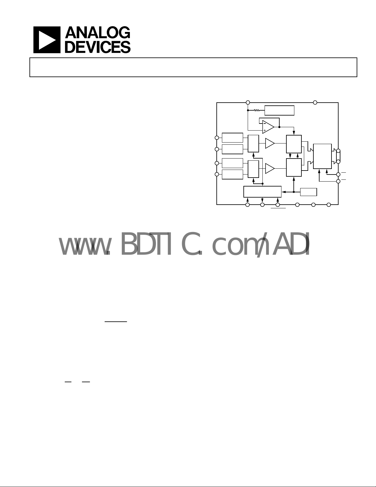
The AD7863 is a high speed, low power, dual 14-bit analog-todigital converter that operates from a single 5 V supply.
The part contains two 5.2 μs successive approximation ADCs, two
track/hold amplifiers, an internal 2.5 V reference and a high speed
parallel interface. Four analog inputs are grouped into two channels
(A and B) selected by the A0 input. Each channel has two inputs
(V
and VA2 or VB1 and VB2) that can be sampled and converted
A1
simultaneously, thus preserving the relative phase information of
the signals on both analog inputs. The part accepts an analog input
range of ±10 V (AD7863-10), ±2.5 V (AD7863-3), and 0 V to
2.5 V (AD7863-2). Overvoltage protection on the analog inputs
for the part allows the input voltage to go to ±17 V, ±7 V, or +7 V
respectively, without causing damage.
A single conversion start signal (
CONVST
both track/holds into hold and initiates conversion on both
channels. The BUSY signal indicates the end of conversion and at
this time the conversion results for both channels are available to be
read. The first read after a conversion accesses the result from V
or V
, and the second read accesses the result from VA2 or VB2,
B1
depending on whether the multiplexer select (A0) is low or high,
respectively. Data is read from the part via a 14-bit parallel data bus
with standard
CS
and RD signals. In addition to the traditional dc
accuracy specifications such as linearity, gain, and offset errors, the
part is also specified for dynamic performance parameters
including harmonic distortion and signal-to-noise ratio.
The AD7863 is fabricated in the Analog Devices, Inc. linear
co
mpatible CMOS (LC
2
MOS) process, a mixed technology
) simultaneously places
A1
Dual 175 kSPS 14-Bit ADC
AD7863
FUNCTIONAL BLOCK DIAGRAM
REF
2kΩ
V
V
V
V
SIGNAL
A1
SCALING
SIGNAL
B1
SCALING
SIGNAL
A2
SCALING
SIGNAL
B2
SCALING
MUX
MUX
CONVERSION
CONTROL L OGIC
BUSY
A0
process that combines precision bipolar circuits with low power
CMOS logic. It is available in 28-lead SOIC_W and SSOP.
PRODUCT HIGHLIGHTS
1. The AD7863 features two complete ADC functions
allowing simultaneous sampling and conversion of two
channels. Each ADC has a two-channel input mux. The
conversion result for both channels is available 5.2 μs after
initiating conversion.
2. The AD7863 op
consumes 70 mW typical. The automatic power-down
mode, where the part goes into power-down once
conversion is complete and wakes up before the next
conversion cycle, makes the AD7863 ideal for batterypowered or portable applications.
3. T
he part offers a high speed parallel interface for easy
connection to microprocessors, microcontrollers, and
digital signal processors.
4. The p
art is offered in three versions with different analog
input ranges. The AD7863-10 offers the standard industrial
input range of ±10 V; the AD7863-3 offers the common
signal processing input range of ±2.5 V, while the AD7863-2
can be used in unipolar 0 V to 2.5 V applications.
5. The p
art features very tight aperture delay matching
between the two input sample and hold amplifiers.
erates from a single 5 V supply and
2.5V
REFERENCE
TRACK/
HOLD
TRACK/
HOLD
CONVST
Figure 1.
14-BIT
ADC
14-BIT
ADC
CLOCK
AGND AGND
AD7863
OUTPUT
LATCH
DGND
DB0
DB13
CS
RD
06411-001
Rev. B
Information furnished by Analog Devices is believed to be accurate and reliable. However, no
responsibility is assumed by Anal og Devices for its use, nor for any infringements of patents or ot her
rights of third parties that may result from its use. Specifications subject to change without notice. No
license is granted by implication or otherwise under any patent or patent rights of Analog Devices.
Trademarks and registered trademarks are the property of their respective owners.
One Technology Way, P.O. Box 9106, Norwood, MA 02062-9106, U.S.A.
Tel: 781.329.4700 www.analog.com
Fax: 781.461.3113 ©2006 Analog Devices, Inc. All rights reserved.

AD7863
www.BDTIC.com/ADI
TABLE OF CONTENTS
Features.............................................................................................. 1
Effective Number of Bits ........................................................... 14
General Description ......................................................................... 1
Functional Block Diagram .............................................................. 1
Product Highlights ........................................................................... 1
Revision History ............................................................................... 2
Specifications..................................................................................... 3
Timing Characteristics ................................................................ 5
Absolute Maximum Ratings............................................................ 6
ESD Caution.................................................................................. 6
Pin Configuration and Function Descriptions............................. 7
Terminology ...................................................................................... 8
Converter Details.............................................................................. 9
Track-and-Hold Section .............................................................. 9
Reference Section ......................................................................... 9
Circuit Description......................................................................... 10
Analog Input Section ................................................................. 10
Total Harmonic Distortion (THD).......................................... 15
Intermodulation Distortion...................................................... 15
Peak Harmonic or Spurious Noise........................................... 15
DC Linearity Plot ....................................................................... 15
Power Considerations................................................................ 16
Microprocessor Interfacing........................................................... 17
AD7863 to ADSP-2100 Interface ............................................. 17
AD7863 to ADSP-2101/ADSP-2102 Interface ....................... 17
AD7863 to TMS32010 Interface .............................................. 17
AD7863 to TMS320C25 Interface............................................ 17
AD7863 to MC68000 Interface ................................................ 18
AD7863 to 80C196 Interface .................................................... 18
Vector Motor Control................................................................ 18
Multiple AD7863s ...................................................................... 19
Applications Hints.......................................................................... 20
Offset and Full-Scale Adjustment ............................................ 10
Timing and Control ................................................................... 11
Operating Modes............................................................................ 13
Mode 1 Operation ...................................................................... 13
Mode 2 Operation ...................................................................... 13
AD7863 Dynamic Specifications ............................................. 14
Signal-to-Noise Ratio (SNR)..................................................... 14
REVISION HISTORY
11/06—Rev. A to Rev. B
Updated Format..................................................................Universal
Deleted Applications ........................................................................ 1
Changes to Specifications................................................................ 3
Changes to Absolute Maximum Ratings....................................... 6
Updated Outline Dimensions....................................................... 21
Changes to Ordering Guide.......................................................... 22
5/99—Rev. 0 to Rev. A
PC Board Layout Considerations............................................. 20
Ground Planes ............................................................................ 20
Power Planes ............................................................................... 20
Supply Decoupling..................................................................... 20
Outline Dimensions....................................................................... 21
Ordering Guide .......................................................................... 22
Rev. B | Page 2 of 24

AD7863
www.BDTIC.com/ADI
SPECIFICATIONS
VDD = 5 V ± 5%, AGND = DGND = 0 V, REF = Internal. All specifications T
MIN
to T
, unless otherwise noted.
MAX
Table 1.
Parameter A Version1 B Version
SAMPLE AND HOLD
−3 dB Small Signal Bandwidth 7 7 MHz typ
Aperture Delay2 35 35 ns max
Aperture Jitter2 50 50 ps typ
Aperture Delay Matching2 350 350 ps max
DYNAMIC PERFORMANCE3 fIN = 80.0 kHz, fS = 175 kSPS
Signal-to-(Noise + Distortion) Ratio4
@ 25°C 78 78 dB min
T
to T
MIN
Total Harmonic Distortion4 −82 −82 dB max −87 dB typ
Peak Harmonic or Spurious Noise4 −82 −82 dB max −90 dB typ
Intermodulation Distortion4 fa = 49 kHz, fb = 50 kHz
Second Order Terms −93 −93 dB typ
Third Order Terms −89 −89 dB typ
Channel-to-Channel Isolation4 −86 −86 dB typ fIN = 50 kHz sine wave
DC ACCURACY Any channel
Resolution 14 14 Bits
Minimum Resolution for Which No
Missing Codes are Guaranteed 14 14 Bits
Relative Accuracy4 ±2.5 ±2 LSB max
Differential Nonlinearity4 +2 to −1 +2 to −1 LSB max
AD7863-10, AD7863-3
Positive Gain Error4 ±10 ±8 LSB max
Positive Gain Error Match4 10 10 LSB max
Negative Gain Error4 ±10 ±8 LSB max
Negative Gain Error Match4 10 10 LSB max
Bipolar Zero Error ±10 ±8 LSB max
Bipolar Zero Error Match 8 6 LSB max
AD7863-2
Positive Gain Error4 ±14 LSB max
Positive Gain Error Match4 16 LSB max
Unipolar Offset Error ±14 LSB max
Unipolar Offset Error Match 10 LSB max
ANALOG INPUTS
AD7863-10
Input Voltage Range ±10 ±10 V
Input Resistance 9 9 kΩ typ
AD7863-3
Input Voltage Range ±2.5 ±2.5 V
Input Resistance 3 3 kΩ typ
AD7863-2
Input Voltage Range 2.5 2.5 V
Input Current 100 100 nA max
77 77 dB min
MAX
1
Unit Test Conditions/Comments
Rev. B | Page 3 of 24

AD7863
www.BDTIC.com/ADI
Parameter A Version1 B Version
1
Unit Test Conditions/Comments
REFERENCE INPUT/OUTPUT
REF IN Input Voltage Range 2.375 to 2.625 2.375 to 2.625 V 2.5 V ± 5%
REF IN Input Current ±100 ±100 μA max
REF OUT Output Voltage 2.5 2.5 V nom
REF OUT Error @ 25°C ±10 ±10 mV max
REF OUT Error T
MIN
to T
±20 ±20 mV max
MAX
REF OUT Temperature Coefficient 25 25 ppm/°C typ
LOGIC INPUTS
Input High Voltage, V
Input Low Voltage, V
2.4 2.4 V min VDD = 5 V ± 5%
INH
0.8 0.8 V max VDD = 5 V ± 5%
INL
Input Current, IIN ±10 ±10 μA max
Input Capacitance, C
5
IN
10 10 pF max
LOGIC OUTPUTS
Output High Voltage, VOH 4.0 4.0 V min I
Output Low Voltage, VOL 0.4 0.4 V max I
= 200 μA
SOURCE
= 1.6 mA
SINK
DB11 to DB0
Floating-State Leakage Current ±10 ±10 μA max
Floating-State Capacitance5 10 10 pF max
Output Coding
AD7863-10, AD7863-3 Twos complement
AD7863-2 Straight (natural) binary
CONVERSION RATE
Conversion Time
Mode 1 Operation 5.2 5.2 μs max For both channels
Mode 2 Operation
Track/Hold Acquisition Time
6
4, 7
0.5 0.5 μs max
10.0 10.0 μs max For both channels
POWER REQUIREMENTS
VDD 5 5 V nom ±5% for specified performance
IDD
Normal Mode (Mode 1)
AD7863-10 18 18 mA max
AD7863-3 16 16 mA max
AD7863-2 11 11 mA max
Power-Down Mode (Mode 2)
IDD @ 25°C8 20 20 μA max 40 nA typ. Logic inputs = 0 V or VDD
Power Dissipation
Normal Mode (Mode 1)
AD7863-10 94.50 94.50 mW max VDD = 5.25 V, 70 mW typ
AD7863-3 84 84 mW max VDD = 5.25 V, 70 mW typ
AD7863-2 57.75 57.75 mW max VDD = 5.25 V, 45 mW typ
Power-Down Mode @ 25°C 105 105 μW max 210 nW typ, VDD = 5.25 V
1
Temperature ranges are as follows: A Version and B Version, −40°C to +85°C.
2
Sample tested during initial release.
3
Applies to Mode 1 operation. See Operating Modes section.
4
See Terminology section.
5
Sample tested @ 25°C to ensure compliance.
6
This 10 μs includes the wake-up time from standby. This wake-up time is timed from the rising edge of
CONVST
, for a narrow
CONVST
the
7
Performance measured through full channel (multiplexer, SHA, and ADC).
8
For best dynamic performance of the AD7863, ATE device testing has to be performed with power supply decoupling in place. In the AD7863 power-down mode of
operation, the leakage current associated with these decoupling capacitors is greater than that of the AD7863 supply current. Therefore, the 40 nA typical figure
shown is characterized and guaranteed by design figure, which reflects the supply current of the AD7863 without decoupling in place. The maximum figure shown in
the Conditions/Comments column reflects the AD7863 with supply decoupling in place—0.1 μF in parallel with 10 μF disc ceramic capacitors on the V
2 × 0.1 μF disc ceramic capacitors on the V
pulse width is greater than 5.2 μs, the effective conversion time increases beyond 10 μs.
CONVST
pulse width the conversion time is effectively the wake-up time plus conversion time, 10 μs. This can be seen from Figure 6. Note that if
pin, in both cases to the AGND plane.
REF
CONVST
, whereas conversion is timed from the falling edge of
pin and
DD
Rev. B | Page 4 of 24

AD7863
www.BDTIC.com/ADI
TIMING CHARACTERISTICS
VDD = 5 V ± 5%, AGND = DGND = 0 V, REF = Internal. All specifications T
MIN
to T
, unless otherwise noted.
MAX
Table 2.
Parameter
t
CONV
t
ACQ
1, 2
A, B Versions Unit Test Conditions/Comments
5.2 μs max Conversion time
0.5 μs max Acquisition time
Parallel Interface
t1 0 ns min
t2 0 ns min
t3 35 ns min
t4 45 ns min
3
t
5
4
t
6
30 ns min
5 ns min
to RD setup time
CS
to RD hold time
CS
CONVST
RD
pulse width
pulse width
Data access time after falling edge of RD
Bus relinquish time after rising edge of RD
30 ns max
t7 10 ns min Time between consecutive reads
t8 400 ns min Quiet time
1
Sample tested at 25°C to ensure compliance. All input signals are measured with tr = tf = 1 ns (10% to 90% of 5 V) and timed from a voltage level of 1.6 V.
2
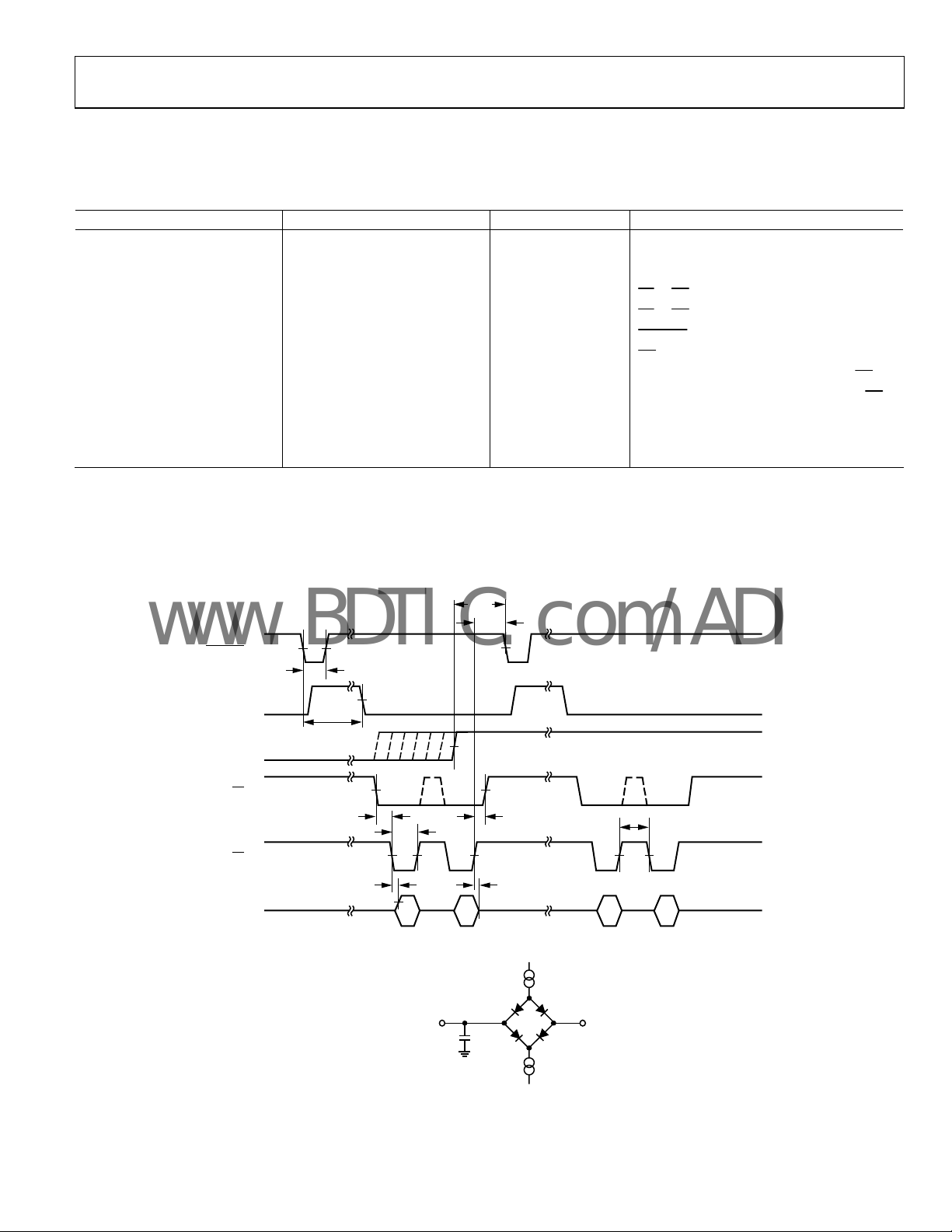
See Figure 2.
3
Measured with the load circuit of Figure 3 and defined as the time required for an output to cross 0.8 V or 2.0 V.
4
These times are derived from the measured time taken by the data outputs to change 0.5 V when loaded with the circuit of Figure 3. The measured number is then
extrapolated back to remove the effects of charging or discharging the 50 pF capacitor. This means that the times quoted in the timing characteristics are the true bus
relinquish times of the part and as such are independent of external bus loading capacitances.
t
ACQ
t
8
CONVST
t
3
BUSY
CS
RD
DATA
t
= 5.2µs
A0
CONV
t
1
t
4
t
5
V
A1
t
2
t
6
V
A2
t
7
V
B1
V
B2
06411-002
Figure 2. Timing Diagram
1.6mA
TO OUTPUT
PIN
50pF
200µA
06411-003
Figure 3. Load Circuit for Access Time and Bus Relinquish Time
Rev. B | Page 5 of 24

AD7863
www.BDTIC.com/ADI
ABSOLUTE MAXIMUM RATINGS
TA = 25°C, unless otherwise noted.
Table 3.
Parameter Ratings
VDD to AGND −0.3 V to +7 V
VDD to DGND −0.3 V to +7 V
Analog Input Voltage to AGND
AD7863-10 ±17 V
AD7863-3 ±7 V
AD7863-2 7 V
Reference Input Voltage to AGND −0.3 V to VDD + 0.3 V
Digital Input Voltage to DGND −0.3 V to VDD + 0.3 V
Digital Output Voltage to DGND −0.3 V to VDD + 0.3 V
Operating Temperature Range
Commercial (A Version and B Version) −40°C to +85°C
Storage Temperature Range −65°C to +150°C
Junction Temperature 150°C
SOIC Package, Power Dissipation 450 mW
θJA Thermal Impedance 71.40°C/W
θJC Thermal Impedance 23.0°C/W
Lead Temperature, Soldering
Vapor Phase (60 sec) 215°C
Infrared (15 sec) 220°C
SSOP Package, Power Dissipation 450 mW
θJA Thermal Impedance 109°C/W
θJC Thermal Impedance 39.0°C/W
Lead Temperature, Soldering
Vapor Phase (60 sec) 215°C
Infrared (15 sec) 220°C
Stresses above those listed under Absolute Maximum Ratings
ma
rating only; functional operation of the device at these or any
other conditions above those indicated in the operational
section of this specification is not implied. Exposure to absolute
maximum rating conditions for extended periods may affect
device reliability.
ESD CAUTION
y cause permanent damage to the device. This is a stress
Rev. B | Page 6 of 24

AD7863
www.BDTIC.com/ADI
PIN CONFIGURATION AND FUNCTION DESCRIPTIONS
DB12
DB11
DB10
DB9
DB8
DB7
DGND
CONVST
DB6
DB5
DB4
DB3
DB2
DB1
1
2
3
4
5
6
AD7863
7
TOP VIEW
(Not to Scale)
8
9
10
11
12
13
14
28
27
26
25
24
23
22
21
20
19
18
17
16
15
DB13
AGND
V
B1
V
A1
V
DD
BUSY
RD
CS
A0
V
REF
V
A2
V
B2
AGND
DB0
06411-004
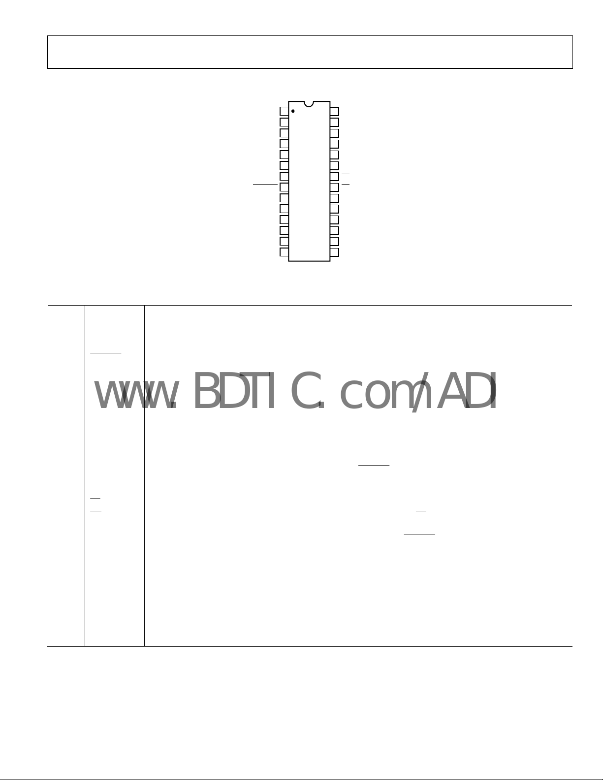
Figure 4. Pin Configuration
Table 4. Pin Function Descriptions
Pin
No. Mnemonic Description
1 to 6 DB12 to DB7 Data Bit 12 to Data Bit 7. Three-state TTL outputs.
7 DGND Digital Ground. Ground reference for digital circuitry.
8
CONVST
Convert Start Input. Logic input. A high-to-low transition on this input puts both track/holds into their hold mode
and starts conversion on both channels.
9 to 15 DB6 to DB0 Data Bit 6 to Data Bit 0. Three-state TTL outputs.
16 AGND Analog Ground. Ground reference for mux, track/hold, reference, and DAC circuitry.
17 VB2
Input Number 2 of Channel B. Analog input voltage ranges of ±10
V (AD7863-10), ±2.5 V (AD7863-3), and 0 V to
2.5 V (AD7863-2).
18 VA2
Input Number 2 of Channel A. Analog input voltage ranges of ±10
V (AD7863-10), ±2.5 V (AD7863-3), and 0 V to
2.5 V (AD7863-2).
19 V
20 A0
REF
Reference Input/Output. This pin is connected to the internal reference through a series resistor and is the output
eference source for the analog-to-digital converter. The nominal reference voltage is 2.5 V, and this appears at the pin.
r
Multiplexer Select. This input is used in conjunction with CONVST
to determine on which pair of channels the
conversion is to be performed. If A0 is low when the conversion is initiated, then channels V
and VB2 are selected.
B1
21
22
selected. If A0 is high when the conversion is initiated, channels V
CS
Read Input. Active low logic input. This input is used in conjunction with CS low to enable the data outputs and
RD
Chip Select Input. Active low logic input. The device is selected when this input is active.
read a conversion result from the AD7863.
23 BUSY
Busy Output. The busy output is triggered high by the falling edge of CONVST
and remains high until conversion
is completed.
24 VDD Analog and Digital Positive Supply Voltage, 5.0 V ± 5%.
25 VA1
Input Number 1 of Channel A. Analog input voltage ranges of ±10
V (AD7863-10), ±2.5 V (AD7863-3), and 0 V to
2.5 V (AD7863-2).
26 VB1
Input Number 1 of Channel B. Analog input voltage ranges of ±10
V (AD7863-10), ±2.5 V (AD7863-3), and 0 V to
2.5 V (AD7863-2).
27 AGND Analog Ground. Ground reference for mux, track/hold, reference, and DAC circuitry.
28 DB13
Data Bit 13 (MSB). Three-state TTL output. Output coding is t
wos complement for the AD7863-10 and AD7863-3.
Output coding is straight (natural) binary for the AD7863-2.
and VA2 are
A1
Rev. B | Page 7 of 24

AD7863
www.BDTIC.com/ADI
TERMINOLOGY
Signal-to-(Noise + Distortion) Ratio
This is the measured ratio of signal to (noise + distortion) at the
utput of the analog-to-digital converter. The signal is the rms
o
amplitude of the fundamental. Noise is the rms sum of all nonfundamental signals up to half the sampling frequency (f
/2),
S
excluding dc. The ratio is dependent upon the number of
quantization levels in the digitization process; the more levels,
the smaller the quantization noise. The theoretical signal-to(noise + distortion) ratio for an ideal N-bit converter with a sine
wave input is given by
Signal to (Noise + Distortion) = (6.02
N + 1.76) dB
For a 14-bit converter, this is 86.04 dB.
Total Harmonic Distortion
Total harmonic distortion (THD) is the ratio of the rms sum of
rmonics to the fundamental. For the AD7863 it is defined as
ha
222
+++
VVVV
5432
()
=
dBTHD
2
log20
V
1
where:
V
is the rms amplitude of the fundamental.
1
, V3, V4, and V5 are the rms amplitudes of the second through
V
2
the fifth harmonics.
Peak Harmonic or Spurious Noise
Peak harmonic or spurious noise is defined as the ratio of the
ms value of the next largest component in the ADC output
r
spectrum (up to f
/2 and excluding dc) to the rms value of the
S
fundamental. Normally, the value of this specification is
determined by the largest harmonic in the spectrum, but for
parts where the harmonics are buried in the noise floor, it is
a noise peak.
Intermodulation Distortion
With inputs consisting of sine waves at two frequencies, fa and
, any active device with nonlinearities creates distortion
fb
products at sum and difference frequencies of mfa ± nfb where
m, n = 0, 1, 2, 3. Intermodulation terms are those for which
neither m nor n is equal to zero. For example, the second order
terms include (fa + fb) and (fa − fb), and the third order terms
include (2fa + fb), (2fa − fb), (fa + 2fb), and (fa − 2fb).
The AD7863 is tested using two input frequencies. In this case,
he second and third order terms are of different significance.
t
The second order terms are usually distanced in frequency from
the original sine waves, and the third order terms are usually at
a frequency close to the input frequencies. As a result, the
second and third order terms are specified separately. The
calculation of the intermodulation distortion is as per the THD
specification where it is the ratio of the rms sum of the
individual distortion products to the rms amplitude of the
fundamental, expressed in decibels (dB).
Rev. B | Page 8 of 24
Channel-to-Channel Isolation
Channel-to-channel isolation is a measure of the level of
cr
osstalk between channels. It is measured by applying a fullscale 50 kHz sine wave signal to all nonselected channels and
determining how much that signal is attenuated in the selected
channel. The figure given is the worst case across all channels.
Relative Accuracy
Relative accuracy or endpoint nonlinearity is the maximum
viation from a straight line passing through the endpoints of
de
the ADC transfer function.
Differential Nonlinearity
This is the difference between the measured and the ideal 1 LSB
ch
ange between any two adjacent codes in the ADC.
Positive Gain Error (AD7863-1
0, ±10 V, AD7863-3, ±2.5 V)
This is the deviation of the last code transition (01 . . . 110 to
01 . . . 111) f
range) or V
rom the ideal 4 × V
− 1 LSB (AD7863-3, ±2.5 V range), after the
REF
− 1 LSB (AD7863-10, ±10 V
REF
bipolar offset error has been adjusted out.
Positive Gain Error (AD7863-2
, 0 V to 2.5 V)
This is the deviation of the last code transition (11 . . . 110 to
11 . . . 111) f
rom the ideal V
− 1 LSB, after the unipolar offset
REF
error has been adjusted out.
Bipolar Zero Error (AD7863-1
0, ±10 V, AD7863-3, ±2.5 V)
This is the deviation of the midscale transition (all 0s to all 1s)
f
rom the ideal 0 V (AGND).
Unipolar Offset Error (AD7863-2, 0 V to 2.5 V)
This is the deviation of the first code transition (00 . . . 000 to
00 . . . 001) f
rom the ideal AGND + 1 LSB.
Negative Gain Error (AD7863-10, ±10 V, AD7863-3, ±2.5 V)
This is the deviation of the first code transition (10 . . . 000 to
. . 001) from the ideal −4 × V
10 .
range) or –V
+ 1 LSB (AD7863-3, ±2.5 V range), after bipolar
REF
+ 1 LSB (AD7863-10, ±10 V
REF
zero error has been adjusted out.
Track-and-Hold Acquisition Time
Track-and-hold acquisition time is the time required for the
utput of the track/hold amplifier to reach its final value, with
o
±½ LSB, after the end of conversion (the point at which the
track-and-hold returns to track mode). It also applies to
situations where a change in the selected input channel takes
place or where there is a step input change on the input voltage
applied to the selected V
input of the AD7863. It means
AX/BX
that the user must wait for the duration of the track-and-hold
acquisition time after the end of conversion or after a channel
change/step input change to V
before starting another
AX/BX
conversion, to ensure that the part operates to specification.
 Loading...