LC2MOS
a
FEATURES
Two-Channel, 8-Bit 2.5 ms ADC
Two 8-Bit, 2.5 ms DACs with Output Amplifiers
Span and Offset of ADC and DAC
Independently Adjustable
Low Power
APPLICATIONS
Winchester Disk Servo Controllers
Floppy Disk Microstepping
Closed Loop Servo Systems
GENERAL DESCRIPTION
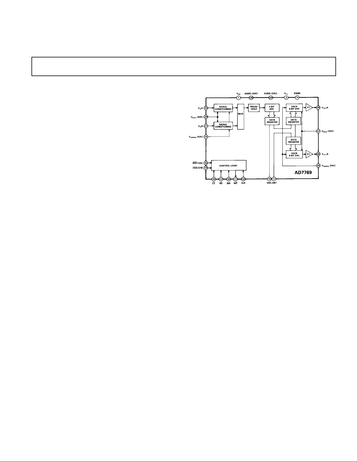
The AD7769 is a complete, two-channel, 8-bit, analog I/O port.
It has versatile input and output signal conditioning features
that make it ideal for use in head-positioning servos in Winchester disk systems. It is equally suitable for floppy disk microstepping head positioning, other closed loop digital servo systems
and general purpose 8-bit data acquisition.
The AD7769 contains a high speed successive approximation
ADC, preceded by a two-channel multiplexer and signal conditioning circuits. The input span of the ADC and the offset of
the zero point from ground can be independently set by applying ground referenced voltages. The AD7769 also contains two
independent, fast settling, 8-bit DACs with output amplifiers.
The output span and offset voltage of the DACs can be set independently of those of the ADC. This makes the AD7769 especially useful in disk drives, where only a positive supply rail is
available and the ranges of the ADC and DACs must be referenced to some positive voltage less than the supply.
The AD7769 is easily interfaced to a standard 8-bit mpu bus via
an 8-bit data port and standard microprocessor control lines.
The AD7769 is fabricated in Linear Compatible CMOS
2
(LC
MOS), an advanced, mixed technology process that combines precision bipolar circuits with low power CMOS logic.
The part is available in a 28-lead plastic DIP and 28-terminal
PLCC package.
Analog I/O Port
AD7769
FUNCTIONAL BLOCK DIAGRAM
PRODUCT HIGHLIGHTS
1. Two-Channel, 8-Bit Analog I/O port on a Single Chip.
The AD7769 contains a two-channel, high speed ADC with
input signal conditioning and two, fast settling 8-bit DACs
with output amplifiers, on a single chip.
2. Independent Control of Span and Offset.
The input voltage span of the ADC and the midpoint of the
transfer function, the output voltage swing of the two DACs
and the half-scale output voltage, can be set independently
by applying ground referenced control voltages.
3. Dynamic Specifications for DSP Users.
In addition to the traditional ADC and DAC specifications,
the AD7769 is specified with ac parameters including signalto-noise ratio, distortion and signal bandwidth.
4. Fast Microprocessor Interface.
The AD7769 has bus interface timing compatible with all
modern microprocessors, with bus access and relinquish
times less than 65 ns and a Write pulse width less than 90 ns.
REV. A
Information furnished by Analog Devices is believed to be accurate and
reliable. However, no responsibility is assumed by Analog Devices for its
use, nor for any infringements of patents or other rights of third parties
which may result from its use. No license is granted by implication or
otherwise under any patent or patent rights of Analog Devices.
One Technology Way, P.O. Box 9106, Norwood, MA 02062-9106,U.S.A.
Tel: 617/329-4700 World Wide Web Site: http://www.analog.comFax:
617/326-8703 © Analog Devices, Inc., 1997

AD7769–SPECIFICA TIONS
(VDD = +12 V 6 10%; VCC = +5 V 6 5%; AGND [ADC] = AGND [DAC] = DGND = 0 V; V
ADC SPECIFICATIONS
V
[ADC] = +2.5 V; f
SWING
= 5 MHz external. All specifications T
CLK
MIN
Parameter J Version A Version Units Conditions/Comments
DC ACCURACY
Resolution 8 * Bits
Relative Accuracy ±1 * LSB max See Terminology
Differential Nonlinearity ±1 * LSB max No Missing Codes. See Terminology.
Bias Offset Error See Terminology
+25°C ±2.5 * LSB max
T
MIN
to T
MAX
±3.0 * LSB max
Bias Offset Match Channel A to Channel B
+25°C ±2.5 * LSB max
T
MIN
to T
MAX
±3.5 * LSB max
Plus or Minus Full-Scale Error See Terminology
+25°C ±2.0 * LSB max
T
MIN
to T
MAX
±2.5 * LSB max
Plus or Minus Full-Scale Match Channel A to Channel B
+25°C ±3.5 * LSB max
T
to T
MIN
MAX
ADC TO DAC MATCHING Channel A/B to V
Bias Offset Match V
±4 * LSB max
(DAC) = +5 V, V
BIAS
OUT
A/B
SWING
+25°C ±2.5 * LSB max
T
MIN
to T
MAX
±3.5 * LSB max
Plus or Minus Full-Scale Match
+25°C ±3.5 * LSB max
T
to T
MIN
MAX
DYNAMIC PERFORMANCE
±4.0 * LSB max
2
Signal-to-Noise Ratio (SNR) 44 * dB min VIN = 100 kHz Full-Scale Sine Wave with f
Total Harmonic Distortion (THD) 48 * dB max VIN = 100 kHz Full-Scale Sine Wave with f
Intermodulation Distortion (IMD) 60 * dB typ f
= 99 kHz, fb = 96.7 kHz with f
a
Frequency Response 0.1 * dB typ VIN = Full-Scale, dc to 200 kHz Sine Wave
ANALOG INPUTS
Input Voltage Ranges, V
A, VINBV
IN
V
BIAS
BIAS
– V
+ V
or 0 V min Whichever Is the Higher
SWING
or 9.8 V max Whichever Is the Lower
SWING
Input Currents, IINA, IINB ±0.4 * mA max
ADC REFERENCE INPUTS
Input Voltage Levels
V
(ADC) 2/6.8 * V min/max With Respect to AGND (ADC). For Specified Performance.
BIAS
V
(ADC) 2.0/3.0 * V min/max With Respect to AGND (ADC). For Specified Performance.
SWING
Input Currents
V
(ADC) Input ±800 * µA max
BIAS
V
(ADC) Input ±1* µA max
SWING
LOGIC OUTPUTS
DB0–DB7,
VOL, Output Low Voltage 0.4 * V max I
V
INT
, Output High Voltage 4.0 * V min I
OH
= 1.6 mA
SINK
SOURCE
= 200 µA
DB0–DB7
Floating State Leakage Current ±10 * µA max
Floating State Capacitance
2
10 * pF max
Output Coding Offset Binary
POWER REQUIREMENTS
V
Range 4.75/5.25 * V min/V max For Specified Performance. The Part Will Function with
CC
VCC =5 V ±10% with Degraded Performance.
V
Range 10.8/13.2 * V min/V max For Specified Performance
DD
I
@ +25°C 20 * mA max For ADC and DAC: V
DD
V
Am VINB = T
UB
MIN
to T
22 * mA max V
MAX
; DAC Code = FF (Hex); DACA and DACB Load = 5 kΩ
BIAS
BIAS
to AGND (DAC). Typically I
I
@ +25°C 5 * mA max Logic Inputs = 2.4 V, CLK Input = 0.8 V. Typically I
CC
T
to T
MIN
MAX
NOTES
1
Temperature range as follows: J Version: 0°C to +70°C; A Version: –40°C to +85°C.
2
Sample tested at +25°C to ensure compliance.
*Specification same as J Version.
Specifications subject to change without notice.
6 * mA max
1
to T
unless otherwise noted.)
MAX
(DAC) = +2.5 V.
SAMPLING
= 5.0 V; V
= 14 mA.
DD
BIAS
SAMPLING
SAMPLlNG
= 400 kHz
= 3.0 V; VINA,
SWING
[ADC] = +5 V;
= 400 kHz
= 400 kHz
= 1.5 mA.
CC
–2–
REV. A
AD7769
(VDD = +12 V 6 10%; VCC = +5 V 6 5%; AGND [DAC] = AGND [ADC] = DGND = 0 V;
V
[DAC] = +5 V; V
BIAS
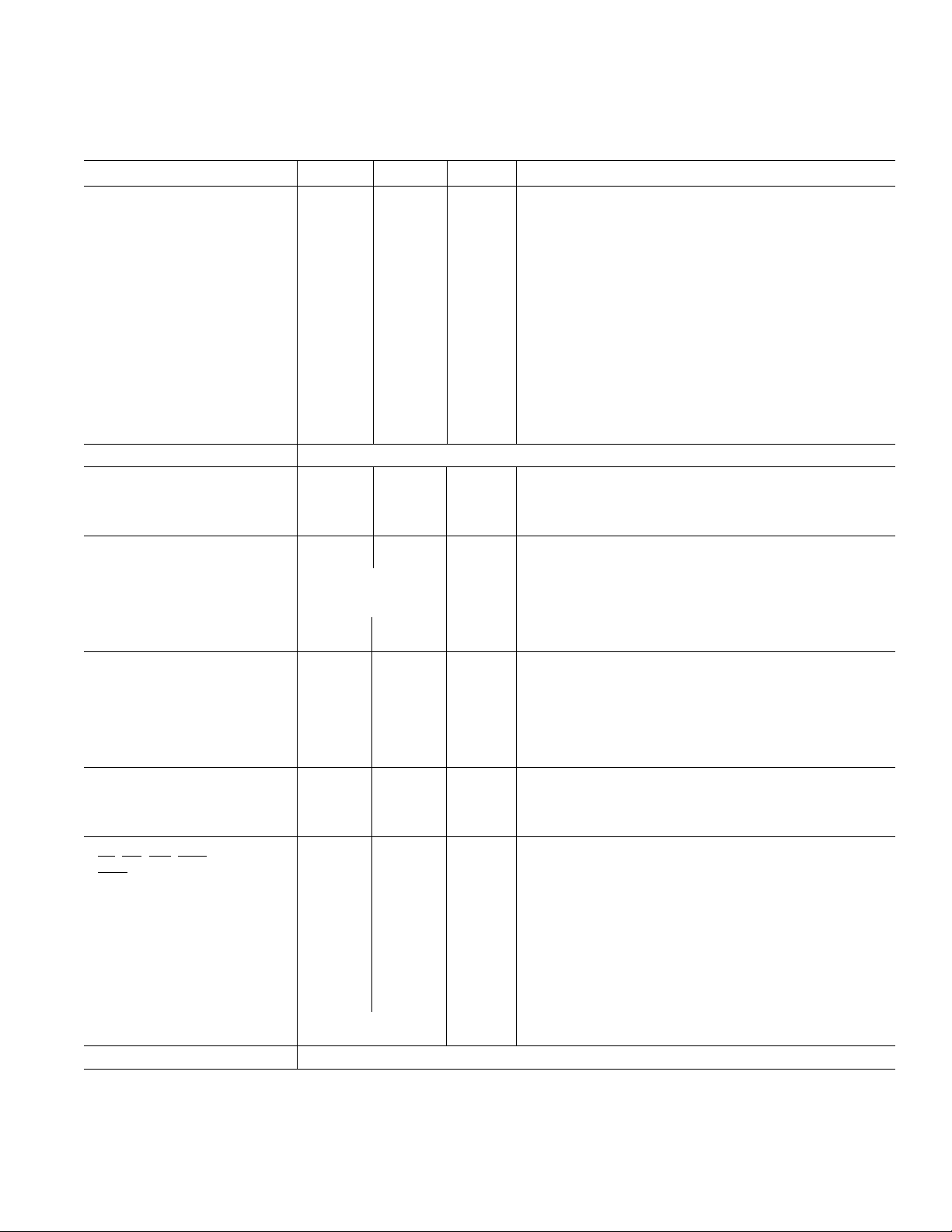
DACA, DACB SPECIFICATIONS
CL = 100 pF. All specifications T
Parameter J Version A Version Units Conditions/Comments
STATIC PERFORMANCE
Resolution 8 * Bits
Relative Accuracy ±1 * LSB max See Terminology
Differential Nonlinearity ±1 * LSB max Guaranteed Monotonic. See Terminology.
Bias Offset Error See Terminology
+25°C ±2.0 * LSB max
to T
T
MIN
MAX
±2.5 * LSB max
Bias Offset Match V
+25°C ±2.5 * LSB max
to T
T
MIN
MAX
±3.5 * LSB max
Plus or Minus Full-Scale Error See Terminology
+25°C ±1.5 * LSB max
to T
T
MIN
MAX
±2.0 * LSB max
Plus or Minus Full-Scale Match V
+25°C ±3.5 * LSB max
T
MIN
to T
MAX
±4.0 * LSB max
ADC to DAC MATCHING As Per ADC Specifications
DYNAMIC PERFORMANCE
2
Signal-to-Noise Ratio (SNR) 44 * dB min V
Total Harmonic Distortion (THD) 48 * dB max V
Intermodulation Distortion (IMD) 55 * dB typ fa = 18.4 kHz, fb = 14.5 kHz with f
ANALOG OUTPUTS
Output Voltage Ranges
A, V
V
OUT
BV
OUT
DC Output Impedance 0.5 *
– V
BIAS
+ V
V
BIAS
–2.0 V max Whichever Is the Lower
V
DD
or 0.5 V min Whichever Is the Higher
SWING
or
SWING
Ω
typ
Short-Circuit Current 20 * mA typ
DAC REFERENCE INPUTS
Input Voltage Levels
(DAC) 3/6.8 * V min/max With Respect to AGND (DAC). For Specified Performance.
V
BIAS
(DAC) 2.0/3.0 * V min/max With Respect to AGND (DAC). For Specified Performance.
V
SWING
Input Currents
(DAC) Input ±2* µA max
V
BIAS
V
(DAC) Input ±1* µA max
SWING
AC CHARACTERISTICS
2
Voltage Output Settling Time 4 * µs max Settling Time to Within ±1/2 LSB of Final Value. Typically 2.5 µs.
Digital-to-Analog Glitch Impulse 30 * nV sec typ See Terminology
Digital Feedthrough 1 * nV sec typ See Terminology
LOGIC INPUTS
CS, RD, WR, ADC/DAC,
CHA/CHB, DB0–DB7
Input Low Voltage, V
Input High Voltage, V
INL
INH
0.8 * V max
2.4 * V min
Input Leakage Current ±10 * µA max
Input Capacitance 10 * pF max
CLK
Input Low Voltage 0.8 * V max External Clock. For Internal Clock Operation Connect
Input High Voltage 2.4 * V min the CLK Pin to V
Input Leakage Current ±10 * µA max
DB0–DB7
Input Coding Offset Binary
POWER REQUIREMENTS As per ADC Specifications
NOTES
1
Temperature range as follows: J Version: 0°C to +70°C; A Version: –40 °C to +85 °C.
2
Sample tested at +25°C to ensure compliance.
*Specifications same as J Version.
Specifications subject to change without notice.
[DAC] = +2.5 V; V
SWING
MIN
A to V
OUT
A to V
OUT
= 20 kHz Full-Scale Sine Wave With f
OUT
= 20 kHz Full-Scale Sine Wave With f
OUT
A, V
OUT
OUT
1
to T
unless otherwise noted.)
MAX
B
OUT
B
OUT
.
DD
B load to AGND [DAC], RL = 5 kV,
= 400 kHz
= 400 kHz
SAMPLING
SAMPLING
SAMPLING
= 400 kHz
REV. A
–3–
AD7769
(VCC = +5 V 6 5%; VDD = +12 V 6 10%; AGND [ADC] = AGND [DAC] = DGND = 0 V.
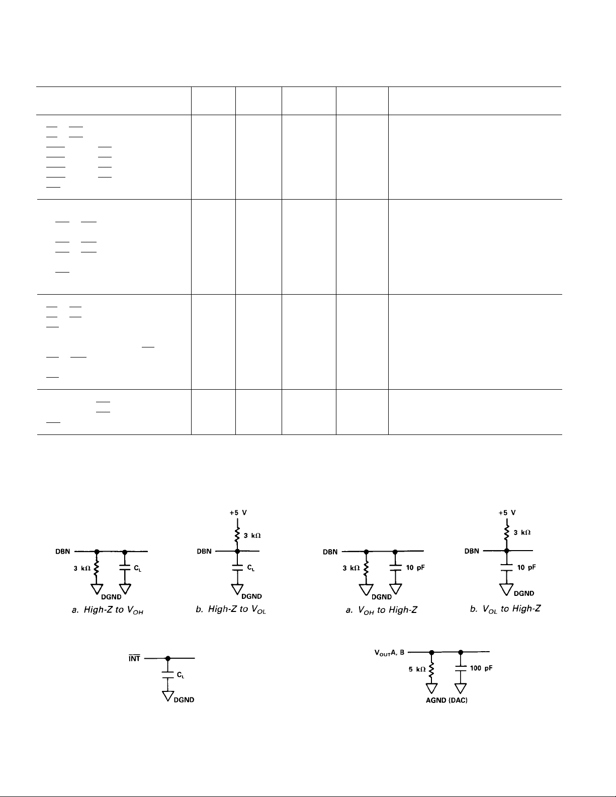
TIMING CHARACTERISTICS
Parameter Label +258CT
ADC /DAC CONTROL TIMING
CS to WR Setup Time t
CS to WR Hold Time t
ADC/DAC to WR Setup Time t
ADC/DAC to WR Hold Time t
CHA/CHB to WR Setup Time t
CHA/CHB to WR Hold Time t
WR Pulse Width t
ADC CONVERSION TIMING
Using External Clock Load Circuit of Figure 3, CL = 20 pF
WR to INT Low Delay t
Using Internal Clock Load Circuit of Figure 3, C
WR to INT Low Delay t
WR to INT High Delay t
WR to Data Valid Delay
ADC READ TIMING
CS to RD Setup Time t
CS to RD Hold Mode t
RD to Data Valid Delay
Bus Relinquish Time after
RD to INT High Delay t
RD Pulse Width t
DAC WRITE TIMING
Data Valid to
Data Valid to
WR Setup Time t
WR Hold Time t
WR to DAC Output Settling Time t
NOTES
1
See Figures 11, 12 and 13.
2
Sample tested at +25°C to ensure compliance. All input signals are specified with tr = tf = 5 ns (10% to 90% of 5 V) and timed from a voltage level of 1.6 V.
3
t10 and t13 are measured with the load circuits of Figure 1 and defined as the time required for an output to cross 0.8 V or 2.4 V.
4
t14 is defined as the time required for the data lines to change 0.5 V when loaded with the circuits of Figure 2.
Specifications subject to change without notice.
3
3
RD High
1, 2
For ADC and DAC, V
Limit at Limit at
1
2
3
4
5
6
7
8
8
9
t
9
t
10
t
10
11
12
t
13
t
4
13
t
14
15
t
15
16
17
18
19
0 0 ns min
0 0 ns min
00 ns
0 0 ns min
0 0 ns min
0 0 ns min
80 80 ns min
2.6 2.6 µs max
1.9/3.0 1.9/3.0 µs min/max Typically 2.5 µs
85 85 ns max Load Circuit of Figure 3, CL = 20 pF
120 120 ns max Load Circuit of Figure 3, CL = 100 pF
t8+70 t8+70 ns max Load Circuit of Figure 1, CL = 20 pF
t8+110 t8+110 ns max Load Circuit of Figure 1, CL = 100 pF
0 0 ns min
0 0 ns min
15/65 15/65 ns min/max Load Circuit of Figure 1, CL = 20 pF
30/100 30/100 ns min/max Load Circuit of Figure 1, CL = 100 pF
15/65 15/65 ns min/max Load Circuit of Figure 2
80 80 ns max Load Circuit of Figure 3, CL = 20 pF
110 110 ns max Load Circuit of Figure 3, CL = 100 pF
t
13
65 65 ns nıin
15 20 ns min
44 µs max Load Circuit of Figure 4
= +5 V, V
BIAS
MIN
t
13
, T
= +2.5 V.)
SWING
Units Test Conditions/Comments
MAX
ns min Determined by t
13
= 20 pF
L
Figure 1. Load Circuits for Data Access Time Test
Figure 3. Load Circuit for
RD
and WR to
INT
Delay Test
–4–
Figure 2. Load Circuits for Bus Relinquish Time Test
Figure 4. Load Circuit for DAC Settling Time Test
REV. A
AD7769
WARNING!
ESD SENSITIVE DEVICE
ABSOLUTE MAXIMUM RATINGS*
VDD to AGND or DGND . . . . . . . . . . . . . . . . .–0.3 V, +15 V
V
to DGND . . . . . . . . . . . . . . . . –0.3 V, VDD +0.3 V or 7 V
CC
(Whichever is Lower)
AGND to DGND . . . . . . . . . . . . . . . . . . –0.3 V, V
+0.3 V
DD
Power Dissipation (Any Package)
to +75°C . . . . . . . . . . . . . . . . . . . . . . . . . . . . . . . . 500 mW
Derates Above +75°C by . . . . . . . . . . . . . . . . . . . 6 mW/°C
Storage Temperature Range . . . . . . . . . . . . –65°C to +150°C
Lead Temperature (Soldering 10 secs) . . . . . . . . . . . .+300°C
Digital Inputs to DGND
(Pins 12, 13, 15–18) . . . . . . . . . . . . . . –0.3 V, V
Digital Outputs to DGND
(Pins 3–10, 11) . . . . . . . . . . . . . . . . . . .–0.3 V, V
Analog Inputs to AGND . . . . . . . . . . . . . –0.3 V, V
Analog Outputs to AGND . . . . . . . . . . . . –0.3 V, V
+0.3 V
DD
+0.3 V
CC
+0.3 V
DD
+0.3 V
DD
*Stresses above those listed under Absolute Maximum Ratings may cause perma-
nent damage to the device. This is a stress rating only; functional operation of the
device at these or any other conditions above those listed in the operational
sections of this specification is not implied. Exposure to absolute maximum rating
conditions for extended periods may affect device reliability. Only one Absolute
Maximum Rating may be applied at any one time.
Operating Temperature Range
Commercial (J Version) . . . . . . . . . . . . . . . . . 0°C to +70°C
Industrial (A Version) . . . . . . . . . . . . . . . . –40°C to +85°C
CAUTION
ESD (electrostatic discharge) sensitive device. Electrostatic charges as high as 4000 V readily
accumulate on the human body and test equipment and can discharge without detection.
Although the AD7769 features proprietary ESD protection circuitry, permanent damage may
occur on devices subjected to high energy electrostatic discharges. Therefore, proper ESD
precautions are recommended to avoid performance degradation or loss of functionality.
ORDERING GUIDE
Temperature Package
Model Range Option*
NOTE
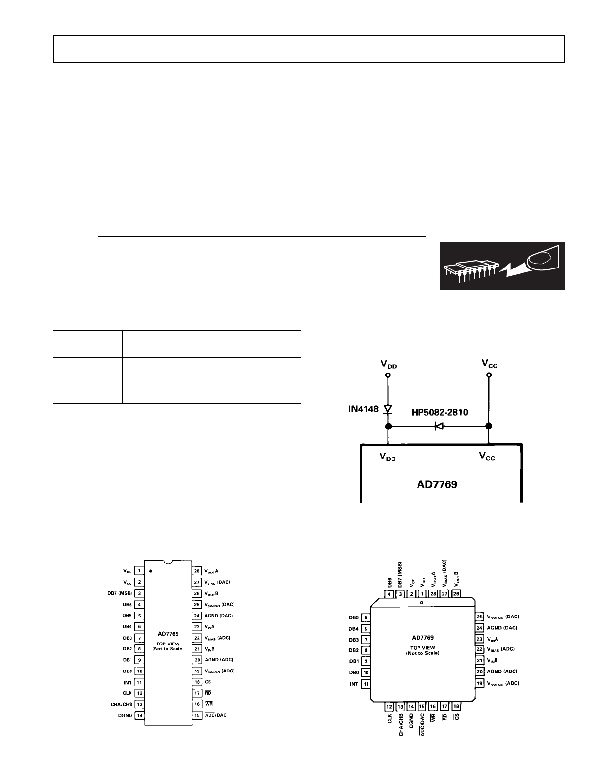
Do not allow V
to exceed VDD by more than 0.3 V. In cases
CC
where this can happen the diode protection scheme shown
below is recommended.
AD7769JN 0°C to +70°C N-28
AD7769JP 0 °C to +70°C P-28A
AD7769AN –40°C to +85°C N-28
AD7769AP –40°C to +85°C P-28A
*N = Plastic DIP; P = Plastic Leaded Chip Carrier.
PIN CONFIGURATIONS
DIP PLCC
REV. A
–5–
 Loading...