24-Bit, 8.5 mW, 109 dB,
FEATURES
Oversampled successive approximation (SAR) architecture
High performance ac and dc accuracy, low power
115.5 dB dynamic range, 32 kSPS (AD7766-2)
112.5 dB dynamic range, 64 kSPS (AD7766-1)
109.5 dB dynamic range, 128 kSPS (AD7766)
−112 dB THD
Exceptionally low power
8.5 mW, 32 kSPS (AD7766-2)
10.5 mW, 64 kSPS (AD7766-1)
15 mW, 128 kSPS (AD7766)
High dc accuracy
24 bits, no missing codes (NMC)
INL: ±6 ppm (typical), ±15 ppm (maximum)
Low temperature drift
Zero error drift: 15 nV/°C
Gain error drift: 0.4 ppm/°C
On-chip low-pass FIR filter
Linear phase response
Pass-band ripple: ±0.005 dB
Stop-band attenuation: 100 dB
2.5 V supply with 1.8 V/2.5 V/3 V/3.6 V logic interface options
Flexible interfacing options
Synchronization of multiple devices
Daisy-chain capability
Power-down function
Temperature range: −40°C to +105°C
APPLICATIONS
Low power PCI/USB data acquisition systems
Low power wireless acquisition systems
Vibration analysis
Instrumentation
High precision medical acquisition
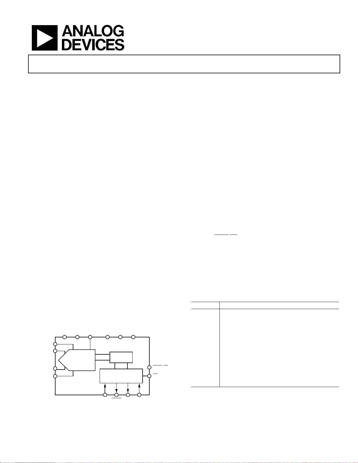
FUNCTIONAL BLOCK DIAGRAM
AVDDAGND MCLK DV
V
REF+
V
IN+
V
IN–
REFGND
Rev. C
Information furnished by Analog Devices is believed to be accurate and reliable. However, no
responsibility is assumed by Analog Devices for its use, nor for any infringements of patents or other
rights of third parties that may result from its use. Specifications subject to change without notice. No
license is granted by implication or otherwise under any patent or patent rights of Analog Devices.
Trademarks and registered trademarks are the property of their respective owners.
SUCCESSIVE
APPROXIMATION
ADC
AD7766/
AD7766-1/
AD7766-2
DDVDRIVE
SERIAL INT ERFACE
CONTRO L LO GIC
SCLK DRDY SDO SDI
Figure 1.
DIGITAL
FIR FILTER
AND
DGND
SYNC/PD
CS
06449-001
128 kSPS/64 kSPS/32 kSPS ADCs
AD7766
GENERAL DESCRIPTION
The AD7766/AD7766-1/AD7766-2 are high performance,
24-bit, oversampled SAR analog-to-digital converters (ADCs).
The AD7766/AD7766-1/AD7766-2 combine the benefits of a
large dynamic range and input bandwidth, consuming 15 mW,
10.5 mW, and 8.5 mW power, respectively, and are contained in
a 16-lead TSSOP package.
Ideal for ultralow power data acquisition (such as PCI- and USBbased systems), the AD7766/AD7766-1/AD7766-2 provide 24-bit
resolution. The combination of exceptional SNR, wide dynamic
range, and outstanding dc accuracy make the AD7766/AD7766-1/
AD7766-2 ideally suited for measuring small signal changes over a
wide dynamic range. This is particularly suitable for applications
where small changes on the input are measured on larger ac or
dc signals. In such an application, the AD7766/AD7766-1/
AD7766-2 accurately gather both ac and dc information.
The AD7766/AD7766-1/AD7766-2 include an on-board digital
filter (complete with linear phase response) that acts to eliminate out-of-band noise by filtering the oversampled input voltage.
The oversampled architecture also reduces front-end antialias
requirements. Other features of the AD7766/AD7766-1/AD7766-2
include a
the synchronization of multiple AD7766/AD7766-1/AD7766-2
devices. The addition of an SDI pin provides the option of daisy
chaining multiple AD7766/AD7766-1/AD7766-2 devices.
The AD7766/AD7766-1/AD7766-2 operate from a 2.5 V supply
using a 5 V reference. The devices operate from −40°C to +105°C.
RELATED DEVICES
Table 1. 24-Bit ADCs
Part No. Description
AD7760 2.5 MSPS, 100 dB dynamic range,1 on-board differential
AD7762/
AD7763
AD7764
AD7765
AD7767
AD7767-1
AD7767-2
1
Dynamic range at maximum output data rate.
One Technology Way, P.O. Box 9106, Norwood, MA 02062-9106, U.S.A.
Tel: 781.329.4700 www.analog.com
Fax: 781.461.3113 ©2007–2010 Analog Devices, Inc. All rights reserved.
SYNC
/PD (synchronization/power-down) pin, allowing
amp and reference buffer, parallel, variable decimation
1
625 kSPS, 109 dB dynamic range,
on-board differential
amp and reference buffer, parallel/serial, variable
decimation
312 kSPS, 109 dB dynamic range,
1
on-board differential
amp and reference buffer, variable decimation (pin)
156 kSPS, 112 dB dynamic range,
1
on-board differential
amp and reference buffer, variable decimation (pin)
128 kSPS, 109.5 dB,
64 kSPS 112.5 dB,
32 kSPS, 115.5 dB,
1
15 mW, 18-bit INL, serial interface
1
10.5 mW, 18-bit INL, serial interface
1
8.5 mW, 18-bit INL, serial interface

AD7766
TABLE OF CONTENTS
Features .............................................................................................. 1
Applications ....................................................................................... 1
Functional Block Diagram .............................................................. 1
General Description ......................................................................... 1
Related Devices ................................................................................. 1
Revision History ............................................................................... 2
Specifications ..................................................................................... 3
Timing Specifications .................................................................. 5
Timing Diagrams .......................................................................... 6
Absolute Maximum Ratings ............................................................ 8
ESD Caution .................................................................................. 8
Pin Configuration and Function Descriptions ............................. 9
Typical Performance Characteristics ........................................... 10
Terminology .................................................................................... 14
Theory of Operation ...................................................................... 15
AD7766/AD7766-1/AD7766-2 Transfer Function ................ 15
Converter Operation .................................................................. 15
Analog Input Structure .............................................................. 16
Supply and Reference Voltages ................................................. 16
AD7766/AD7766-1/AD77662-2 Interface .................................. 17
Initial Power-Up ......................................................................... 17
Reading Data ............................................................................... 17
Power-Down, Reset, and Synchronization ............................. 17
Daisy Chaining ............................................................................... 18
Reading Data in Daisy-Chain Mode ....................................... 18
Choosing the SCLK Frequency ................................................ 18
Daisy-Chain Mode Configuration and Timing Diagrams ... 19
Driving the AD7766/AD7766-1/AD7766-2 ............................... 20
Differential Signal Source ......................................................... 20
Single-Ended Signal Source ...................................................... 20
Antialiasing ................................................................................. 21
Power Dissipation....................................................................... 21
V
Input Signal ....................................................................... 22
REF+
Multiplexing Analog Input Channels ...................................... 22
Outline Dimensions ....................................................................... 23
Ordering Guide .......................................................................... 23
REVISION HISTORY
4/10—Rev. B to Rev. C
Changes to Pin 8 Description ......................................................... 9
Changes to Table 8 .......................................................................... 20
3/09—Rev. A to Rev. B
Changes to t
Changes to Table 7 .......................................................................... 17
1/09—Rev. 0 to Rev. A
Changes to Features Section............................................................ 1
Change to AD7766, Intermodulation Distortion (IMD)
Parameter and Integral Nonlinearity Parameter, Table 2 ....... 3
Change to Figure 21 and Figure 24 .............................................. 12
Changes to Supply and Reference Voltages Section ................... 16
Changes to Choosing the SCLK Frequency Section .................. 18
Changes to Driving the AD7766 Section .................................... 20
Changes to Single-Ended Signal Source Section ........................ 20
Changes to Figure 40 and Figure 41 ............................................. 20
Added Table 8; Renumbered Sequentially .................................. 20
Change to Figure 42 ....................................................................... 21
Changes to Antialiasing Section ................................................... 21
Changes to Table 9 .......................................................................... 21
Changes to V
Changes to Figure 46 ...................................................................... 22
8/07—Revision 0: Initial Version
Parameter, Table 3 .......................................... 5
SETTLING
Input Signal Section ......................................... 22
REF+
Rev. C | Page 2 of 24

AD7766
SPECIFICATIONS
AVDD = DVDD = 2.5 V ± 5%, V
unless otherwise noted.
Table 2.
Parameter Test Conditions/Comments Min Typ Max Unit
OUTPUT DATA RATE (ODR)
AD7766 Decimate by 8 128 kHz
AD7766-1 Decimate by 16 64 kHz
AD7766-2 Decimate by 32 32 kHz
ANALOG INPUT1
Differential Input Voltage V
Absolute Input Voltage V
V
Common-Mode Input Voltage V
Input Capacitance 22 pF
DYNAMIC PERFORMANCE
AD7766 Decimate by 8, ODR = 128 kHz
Dynamic Range2 Shorted inputs 108 109.5 dB
Signal-to-Noise Ratio (SNR)2 Full-scale input amplitude, 1 kHz tone 107 108.5 dB
Spurious-Free Dynamic Range (SFDR)2 Full-scale input amplitude, 1 kHz tone −128 −116 dB
Total Harmonic Distortion (THD)2 Full-scale input amplitude, 1 kHz tone −112 −103 dB
Intermodulation Distortion (IMD)2 Tone A = 49.7 kHz, Tone B = 50.3 kHz
Second-Order Terms −133 dB
Third-Order Terms −109 dB
AD7766-1 Decimate by 16, ODR = 64 kHz
Dynamic Range2 Shorted inputs 111 112.5 dB
Signal-to-Noise Ratio (SNR)
Spurious-Free Dynamic Range (SFDR)2 Full-scale input amplitude, 1 kHz tone −128 −116 dB
Total Harmonic Distortion (THD)
Intermodulation Distortion (IMD)2 Tone A = 24.7 kHz, Tone B = 25.3 kHz dB
Second-Order Terms −133 dB
Third-Order Terms −108 dB
AD7766-2 Decimate by 32, ODR = 32 kHz
Dynamic Range2 Shorted inputs 114 115.5 dB
Signal-to-Noise Ratio (SNR)
Spurious-Free Dynamic Range (SFDR)
Total Harmonic Distortion (THD)
Intermodulation Distortion (IMD)
Second-Order Terms −137 dB
Third-Order Terms −108 dB
DC ACCURACY1 For all devices
Resolution No missing codes 24 Bits
Differential Nonlinearity
Integral Nonlinearity
2
2
Zero Error2 20 V
Gain Error2 0.0075 0.075 % FS
Zero Error Drift2 15 nV/°C
Gain Error Drift2 0.4 ppm/°C
Common-Mode Rejection Ratio2 50 Hz tone −110 dB
= 1.8 V to 3.6 V, V
DRIVE
2
2
2
2
2
2
= 5 V, MCLK = 1 MHz, common-mode input = V
REF+
− V
IN+
IN+
IN−
±V
IN−
−0.1 +V
−0.1 +V
/2 − 5% V
REF+
REF+
/2, TA = −40°C to +105°C,
REF+
V p-p
REF+
+ 0.1 V
REF+
+ 0.1 V
REF+
/2 V
/2 + 5% V
REF+
Full-scale input amplitude, 1 kHz tone 110 111.5 dB
Full-scale input amplitude, 1 kHz tone −112 −103 dB
Full-scale input amplitude, 1 kHz tone 112 113.5 dB
Full-scale input amplitude, 1 kHz tone −128 −116 dB
Full-scale input amplitude, 1 kHz tone −112 −103 dB
Tone A = 11.7 kHz, Tone B = 12.3 kHz dB
Guaranteed monotonic to 24 bits
16-bit linearity ±6 ±15 ppm
Rev. C | Page 3 of 24

AD7766
Parameter Test Conditions/Comments Min Typ Max Unit
DIGITAL FILTER RESPONSE1
Group Delay
Settling Time (Latency) Complete settling 74/ODR µs
Pass-Band Ripple
Pass Band
−3 dB Bandwidth
Stop-Band Frequency
Stop-Band Attenuation
REFERENCE INPUT1
V
Input Voltage 2.4 2 × AVDD V
REF+
DIGITAL INPUTS (Logic Levels)1
VIL −0.3
VIH 0.7 × V
Input Leakage Current ±1 A/pin
Input Capacitance 5 pF
Master Clock Rate 1.024 MHz
Serial Clock Rate 1/t8 Hz
DIGITAL OUTPUTS1
Data Format
VOL I
VOH I
POWER REQUIREMENTS1
AVDD ± 5% 2.5 V
DVDD ± 5% 2.5 V
V
1.7 2.5 3.6 V
DRIVE
CURRENT SPECIFICATIONS MCLK = 1.024 MHz
AD7766 Operational Current 128 kHz output data rate
AIDD 1.3 1.5 mA
DIDD 3.9 4.8 mA
I
0.35 0.425 mA
REF
AD7766-1 Operational Current 64 kHz output data rate
AIDD 1.3 1.5 mA
DIDD 2.2 2.85 mA
I
0.35 0.425 mA
REF
AD7766-2 Operational Current 32 kHz output data rate
AIDD 1.3 1.5 mA
DIDD 1.37 1.86 mA
I
0.35 0.425 mA
REF
Static Current with MCLK Stopped For all devices
AIDD 0.9 1 mA
DIDD 1 93 A
Power-Down Mode Current For all devices
AIDD 0.1 6 A
DIDD 1 93 A
POWER DISSIPATION MCLK = 1.024 MHz
AD7766 Operational Power 128 kHz output data rate 15 18 mW
AD7766-1 Operational Power 64 kHz output data rate 10.5 13 mW
AD7766-2 Operational Power 32 kHz output data rate 8.5 10.5 mW
1
Specifications are for all devices, AD7766, AD7766-1, and AD7766-2.
2
See the Terminology section.
Serial 24 bits, twos complement
37/ODR µs
±0.005 dB
0.453 × ODR Hz
0.49 × ODR Hz
0.547 × ODR Hz
100 dB
DRIVE
+0.3 × V
V
DRIVE
V
DRIVE
+ 0.3 V
(MSB first)
= +500 A 0.4 V
SINK
= −500 µA V
SOURCE
– 0.3 V
DRIVE
Rev. C | Page 4 of 24
AD7766
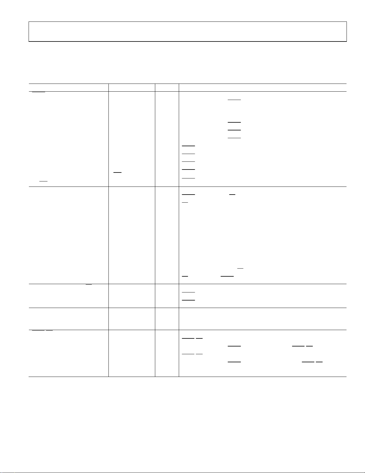
TIMING SPECIFICATIONS
AVDD = DVDD = 2.5 V ± 5%, V
unless otherwise noted.
1
Table 3.
Parameter Limit at t
DRDY OPERATION
t1 510 ns typ
2
t
100 ns min MCLK high pulse width
2
2
t
900 ns max MCLK low pulse width
3
t4 265 ns typ
t5 294 ns typ
3
t
t
READ
3
t
n × 8 × t
DRDY
READ OPERATION
t6 0 ns min
t7 6 ns max
t8 60 ns max Data access time after SCLK falling edge (V
t9 10 ns min SCLK falling edge to data valid hold time (V
t10 10 ns min SCLK high pulse width
t11 10 ns min SCLK low pulse width
t
1/t8 sec min Minimum SCLK period
SCLK
t12 6 ns max
t13 0 ns min
READ OPERATION WITH CS LOW
t14 0 ns min
t15 0 ns max
DAISY-CHAIN OPERATION
t16 1 ns min SDI valid to SCLK falling edge setup time
t17 2 ns max SCLK falling edge to SDI valid hold time
SYNC/PD OPERATION
t18 1 ns typ
t19 20 ns typ
t20 1 ns min
t21 510 ns typ
3
t
(592 × n) + 2 t
SETTLING
1
Sample tested during initial release to ensure compliance. All input signals are specified with tr = tf = 5 ns (10% to 90% of DVDD) and timed from a voltage level of 1.7 V.
2
t2 and t3 allow a ~90% to 10% duty cycle to be used for the MCLK input, where the minimum is 10% for the clock high time and 90% for MCLK low time. The maximum
MCLK frequency is 1.024 MHz.
3
n = 1 for AD7766, n = 2 for the AD7766-1, n = 4 for the AD7766-2.
= 1.7 V to 3.6 V, V
DRIVE
MIN
, t
= 5 V, common-mode input = V
REF+
Unit Description
MAX
/2, TA = −40°C (T
REF+
MCLK rising edge to DRDY
MCLK rising edge to DRDY
128 ns typ
71 ns typ
435 ns typ
492 ns typ
− t5 ns typ
DRDY
ns typ
MCLK
MCLK rising edge to DRDY
MCLK rising edge to DRDY
pulse width (AD7766)
DRDY
pulse width (AD7766-1)
DRDY
pulse width (AD7766-2)
DRDY
low period, read data during this period
DRDY
period
DRDY
falling edge to CS setup time
DRDY
falling edge to SDO tristate disabled
CS
falling edge
rising edge (AD7766)
rising edge (AD7766-1)
rising edge (AD7766-2)
50 ns max Data access time after SCLK falling edge (V
25 ns max Data access time after SCLK falling edge (V
24 ns max Data access time after SCLK falling edge (V
Bus relinquish time after CS
rising edge to DRDY rising edge
CS
rising edge
falling edge to data valid setup time
DRDY
rising edge to data valid hold time
DRDY
/PD falling edge to MCLK rising edge
SYNC
MCLK rising edge to DRDY
/PD rising edge to MCLK rising edge
SYNC
MCLK rising edge to DRDY
Filter settling time after a reset or power-down
MCLK
rising edge going into SYNC/PD mode
falling edge coming out of SYNC/PD mode
) to +105°C (T
MIN
= 1.7 V)
DRIVE
= 2.3 V)
DRIVE
= 2.7 V)
DRIVE
= 3.0 V)
DRIVE
= 3.6 V)
DRIVE
MAX
),
Rev. C | Page 5 of 24
AD7766
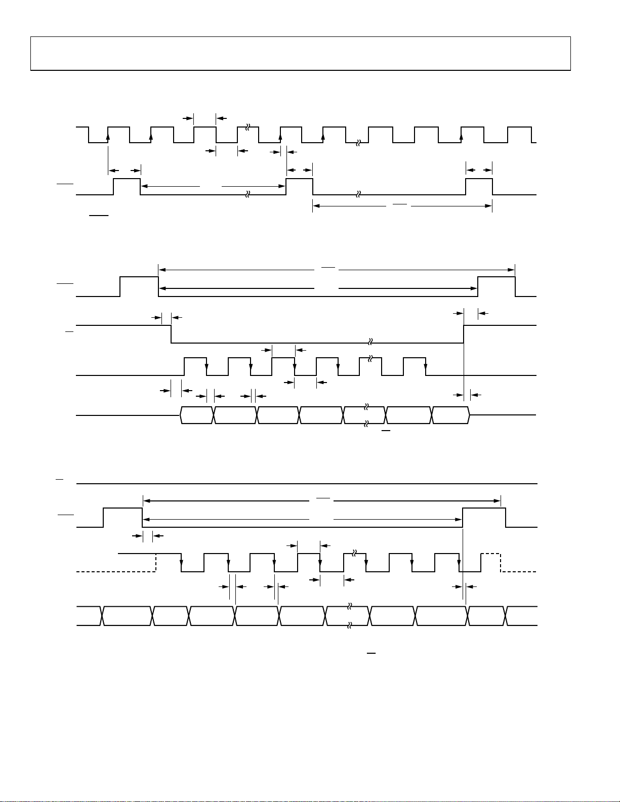
TIMING DIAGRAMS
t
2
MCLK
DRDY
Figure 2.
DRDY
vs. MCLK Timing Diagram, n = 1 for AD7766 (Decimate by 8), n = 2 for AD7766-1 (Decimate by 16), n = 4 for AD7766-2 (Decimate by 32)
1
t
3
t
1
t
READ
8 × n 8 × n1
t
4
t
5
t
DRDY
t
DRDY
t
5
06449-002
DRDY
SCLK
SDO
CS
t
6
t
10
1 23
t
t
7
8
t
9
D22MSB D21 D20 D1 LSB
Figure 3. Serial Timing Diagram, Reading Data Using
t
READ
t
13
t
11
t
12
06449-003
CS
CS = 0
t
DRDY
DRDY
SCLK
t
14
1 23 24
t
8
t
READ
t
10
t
t
9
11
t
15
SDO
DATA
INVALID
MSB D22 D21 D20 D1 LSB
CS
Figure 4. Serial Timing Diagram, Reading Data Setting
Logic Low
Rev. C | Page 6 of 24
DATA
INVALID
06449-004
AD7766
S
PART OUT OF POWER-DOWN
FILTER RESET
t
20
INVALID DATA VALID DATAVALID DATA
BEGINS SAMPL ING
t
SETTLING
MCLK (I)
YNC/PD (I)
DRDY (O)
SDO (O)
PART IN POWER-DOWN
ABCD
t
18
t
19
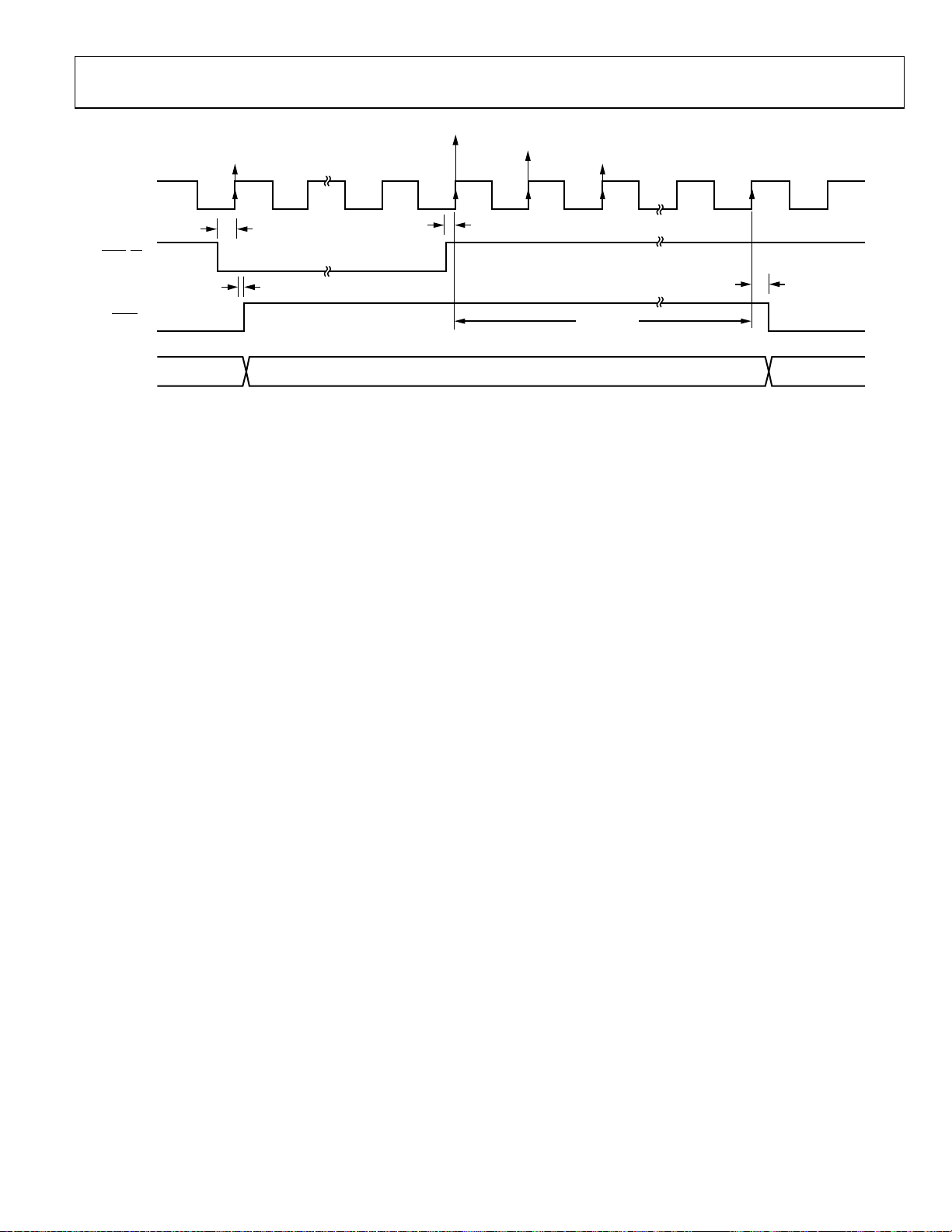
Figure 5. Reset, Synchronization, and Power-Down Timing (For More Information, See the Power-Down, Reset, and Synchronization Section)
t
21
06449-005
Rev. C | Page 7 of 24
AD7766
ABSOLUTE MAXIMUM RATINGS
TA = 25°C, unless otherwise noted.
Table 4.
Parameter Rating
AV
to AGND −0.3 V to +3 V
DD
DVDD to DGND −0.3 V to +3 V
AVDD to DVDD −0.3 V to +0.3 V
V
to REFGND −0.3 V to +7 V
REF+
REFGND to AGND −0.3 V to +0.3 V
V
to DGND −0.3 V to +6 V
DRIVE
V
to AGND −0.3 V to V
IN+, VIN–
Digital Inputs to DGND −0.3 V to V
Digital Outputs to DGND −0.3 V to V
REF+
DRIVE
DRIVE
+ 0.3 V
+ 0.3 V
+ 0.3 V
AGND to DGND −0.3 V to +0.3 V
Input Current to Any Pin Except
Supplies
1
±10 mA
Operating Temperature Range −40°C to +105°C
Storage Temperature Range −65°C to +150°C
Junction Temperature 150°C
TSSOP Package
θ
Thermal Impedance 150.4°C/W
JA
θ
Thermal Impedance 27.6°C/W
JC
Lead Temperature, Soldering
Vapor Phase (60 sec) 215°C
Infrared (15 sec) 220°C
ESD 1 kV
1
Transient currents of up to 100 mA do not cause SCR latch-up.
Stresses above those listed under Absolute Maximum Ratings
may cause permanent damage to the device. This is a stress
rating only; functional operation of the device at these or any
other conditions above those indicated in the operational
section of this specification is not implied. Exposure to absolute
maximum rating conditions for extended periods may affect
device reliability.
ESD CAUTION
Rev. C | Page 8 of 24
 Loading...