Analog Devices AD7739 Datasheet
A
8-Channel, High Throughput,
FEATURES
High resolution ADC
24 bits no missing codes
±0.0015% nonlinearity
Optimized for fast channel switching
18-bit p-p resolution (21 bits effective) at 500 Hz
16-bit p-p resolution (19 bits effective) at 4 kHz
On-chip per channel system calibration
Configurable inputs
8 single-ended or 4 fully differential
Input ranges
+625 mV, ±625 mV, +1.25 V, ±1.25 V, +2.5 V, ±2.5 V
3-wire serial interface
SPI®, QSPI™, MICROWIRE™, and DSP compatible
Schmitt trigger on logic inputs
Single-supply operation
5 V analog supply
3 V or 5 V digital supply
Package: 24-lead TSSOP
24-Bit ∑-∆ ADC
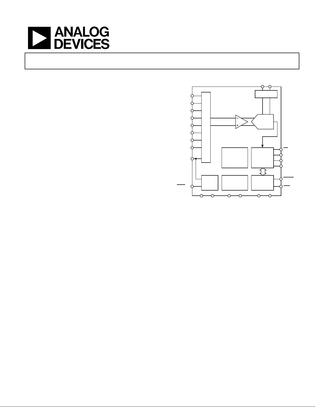
FUNCTIONAL BLOCK DIAGRAM
AIN0
AIN1
AIN2
AIN3
AIN4
AIN5
AIN6
AIN7
INCOM/P0
SYNC/P1
MUX
I/O PORT
BUFFER
AD7739
CALIBRATION
CIRCUITRY
CLOCK
GENERATOR
AD7739
REFIN(–) REFIN(+)
REFERENCE
DETECT
24-BIT
Σ-∆ ADC
SERIAL
INTERFACE
CONTROL
LOGIC
CS
SCLK
DOUT
DIN
RESET
RDY
APPLICATIONS
PLCs/DCSs
Multiplexing applications
Process control
Industrial instrumentation
GENERAL DESCRIPTION
The AD7739 is a high precision, high throughput analog front
end. True 16-bit p-p resolution is achievable with a total
conversion time of 250 µs (4 kHz channel switching), making it
ideally suited to high resolution multiplexing applications.
The part can be configured via a simple digital interface, which
allows users to balance the noise performance against data
throughput up to 15 kHz.
The analog front end features eight single-ended or four fully
differential input channels with unipolar or bipolar 625 mV,
1.25 V, and 2.5 V input ranges. It accepts a common-mode input
voltage from 200 mV above AGND to AV
The differential reference input features “No-Reference” detect
capability. The ADC also supports per channel system
calibration options.
– 300 mV.
DD
DGND DV
DD
MCLKINMCLKOUTAGND AV
Figure 1.
03742-0-001
DD
The digital serial interface can be configured for 3-wire
operation and is compatible with microcontrollers and digital
signal processors. All interface inputs are Schmitt triggered.
The part is specified for operation over the extended industrial
temperature range of –40°C to +105°C.
Other parts in the AD7739 family are the AD7738, AD7734,
and AD7732.
The AD7738 is similar to the AD7739 but has higher speed
(8.5 kHz channel switching for 16-bit performance) and higher
AIN leakage current. The AD7738 multiplexer output is pinned
out externally, allowing the user to implement programmable
gain or signal conditioning before being applied to the ADC.
The AD7734 analog front end features four single-ended input
channels with unipolar or true bipolar input ranges to ±10 V
while operating from a single +5 V analog supply. The AD7734
accepts an analog input overvoltage to ±16.5 V without
degrading the performance of the adjacent channels.
The AD7732 is similar to the AD7734, but its analog front end
features two fully differential input channels.
Rev. 0
Information furnished by Analog Devices is believed to be accurate and reliable.
However, no responsibility is assumed by Analog Devices for its use, nor for any
infringements of patents or other rights of third parties that may result from its use.
Specifications subject to change without notice. No license is granted by implication
or otherwise under any patent or patent rights of Analog Devices. Trademarks and
registered trademarks are the property of their respective companies.
One Technology Way, P.O. Box 9106, Norwood, MA 02062-9106, U.S.A.
Tel: 781.329.4700
Fax: 781.326.8703 © 2003 Analog Devices, Inc. All rights reserved.
www.analog.com

AD7739
TABLE OF CONTENTS
AD7739—Specifications.................................................................. 3
Digital Interface Description ........................................................ 22
Timing Specifications....................................................................... 6
Absolute Maximum Ratings............................................................ 8
Typical Performance Characteristics ............................................. 9
Output Noise and Resolution Specification................................ 10
Chopping Enabled...................................................................... 10
Chopping Disabled..................................................................... 11
Pin Configuration and Function Descriptions........................... 12
Register Descriptions ..................................................................... 14
Register Access............................................................................ 15
Communications Register......................................................... 15
I/O Port Register......................................................................... 16
Revision Register ........................................................................16
Test Register ................................................................................ 16
ADC Status Register................................................................... 17
Checksum Register..................................................................... 17
Hardware ..................................................................................... 22
Reset ............................................................................................. 23
Access the AD7739 Registers.................................................... 23
Single Conversion and Reading Data...................................... 23
Dump Mode................................................................................ 23
Continuous Conversion Mode ................................................. 24
Continuous Read (Continuous Conversion) Mode .............. 25
Circuit Description......................................................................... 26
Analog Inputs.............................................................................. 26
Sigma-Delta ADC....................................................................... 26
Chopping..................................................................................... 26
Multiplexer, Conversion, and Data Output Timing............... 27
Frequency Response .................................................................. 28
Analog Input’s Extended Voltage Range ................................. 29
Voltage Reference Inputs........................................................... 29
ADC Zero-Scale Calibration Register ..................................... 17
ADC Full-Scale Calibration Register....................................... 17
Channel Data Registers ............................................................. 17
Channel Zero-Scale Calibration Registers.............................. 18
Channel Full-Scale Calibration Registers................................ 18
Channel Status Registers ...........................................................18
Channel Setup Registers............................................................ 19
Channel Conversion Time Registers ....................................... 20
Mode Register ............................................................................. 20
REVISION HISTORY
Revision 0: Initial Version
Reference Detect......................................................................... 29
I/O Port........................................................................................ 29
Calibration................................................................................... 30
ADC Zero-Scale Self-Calibration ........................................ 30
ADC Full-Scale Self-Calibration.......................................... 30
Per Channel System Calibration .......................................... 30
Outline Dimensions....................................................................... 32
ESD Caution................................................................................ 32
Ordering Guide .......................................................................... 32
Rev. 0 | Page 2 of 32

AD7739
AD7739—SPECIFICATIONS
Table 1. (–40°C to +105°C; AVDD = 5 V ± 5%; DVDD = 2.7 V to 3.6 V, or 5 V ± 5%; REFIN(+) = 2.5 V; REFIN(–) = 0 V,
AINCOM = 2.5 V; Internal Buffer On, AIN Range = ±1.25 V; f
Parameter Min Typ Max Unit Test Conditions/Comments
ADC PERFORMANCE
CHOPPING ENABLED
Conversion Time Rate 372 11840 Hz Configure via Conv. Time Register
No Missing Codes
1, 2
24 Bits
Output Noise See Table 4
Resolution
See Table 5
and Table 6
Integral Nonlinearity (INL)2 ±5 ±0.0015 % of FSR
Offset Error (Unipolar, Bipolar)3 ±10 µV Before Calibration
Offset Drift vs. Temperature1 ±25 nV/°C
Gain Error3 ±0.2 % Before Calibration
Gain Drift vs. Temperature1 ±2.5 ppm of FS/°C
Positive Full-Scale Error3 ±0.2 % of FSR Before Calibration
Positive Full-Scale Drift vs. Temp.1 ±2.5 ppm of FS/°C
Bipolar Negative Full-Scale Error4 ±0.0030 % of FSR After Calibration
Common-Mode Rejection 80 95 dB At DC, AIN = 1 V
Power Supply Rejection 70 80 dB At DC, AIN = 1 V
ADC PERFORMANCE
CHOPPING DISABLED
Conversion Time Rate 737 15133 Hz Configure via Conv. Time Register
No Missing Codes
1, 2
24 Bits
Output Noise See Table 7
Resolution
See Table 8
and Table 9
Integral Nonlinearity (INL)2 ±0.0015 % of FSR
Offset Error (Unipolar, Bipolar)5 ±1mV mV Before Calibration
Offset Drift vs. Temperature ±1.5 µV/°C
Gain Error3 ±0.2 % Before Calibration
Gain Drift vs. Temperature ±2.5 ppm of FS/°C
Positive Full-Scale Error3 ±0.2 % of FSR Before Calibration
Positive Full-Scale Drift vs. Temp. ±2.5 ppm of FS/°C
Bipolar Negative Full-Scale Error4 ±0.0030 % of FSR After Calibration
Common-Mode Rejection 75 dB At DC, AIN = 1 V
Power Supply Rejection 65 dB At DC, AIN = 1 V
ANALOG INPUTS
Analog Input Voltage
1, 6
±2.5 V Range ±2.5 V
+2.5 V Range 0 to +2.5 V
±1.25 V Range ±1.25 V
+1.25 V Range 0 to +1.25 V
±0.625 V Range ±0.625 V
+0.625 V Range 0 to +0.625 V
AIN, AINCOM Common-Mode/
Absolute Voltage
Analog Input Slew Rate
AIN, AINCOM Input Current
1
1, 7
0.5 V/Conv. Time AIN Absolute Voltage > 3 V
1, 8
1 5 nA Only One Channel, Chop Disabled
0.2 AV
= 6.144 MHz; unless otherwise noted.)
MCLKIN
FW ≥ 12 (Conversion Time ≥ 290 µs)
FW ≥ 12 (Conversion Time ≥ 290 µs)
– 0.3 V
DD
Rev. 0 | Page 3 of 32

AD7739
Parameter Min Typ Max Unit Test Conditions/Comments
REFERENCE INPUTS
REFIN(+) to REFIN(–) Voltage
NOREF Trigger Voltage 0.5 V NOREF Bit in Channel Status Register
REFIN(+), REFIN(–) Common-Mode/
Absolute Voltage
1
Reference Input DC Current10 400 µA
SYSTEM CALIBRATION
1, 11
Full-Scale Calibration Limit
Zero-Scale Calibration Limit
Input Span
LOGIC INPUTS
Input Current
Input Current CS
–40 µA
Input Capacitance 5 pF
1
V
1.4 2 V DVDD = 5 V
T+
1
V
0.8 1.4 V DVDD = 5 V
T–
VT+ – V
V
1
0.3 0.85 V DVDD = 5 V
T–
1
0.95 2 V DVDD = 3 V
T+
VT– 1 0.4 1.1 V DVDD = 3 V
VT+ – V
1
0.3 0.85 V DVDD = 3 V
T–
MCLK IN ONLY
Input Current
Input Capacitance 5 pF
V
Input Low Voltage 0.8 V DVDD = 5 V
INL
V
Input High Voltage 3.5 V DVDD = 5 V
INH
V
Input Low Voltage 0.4 V DVDD = 3 V
INL
V
Input High Voltage 2.5 V DVDD = 3 V
INH
LOGIC OUTPUTS12
VOL Output Low Voltage 0.4 V I
VOH Output High Voltage 4.0 V I
VOL Output Low Voltage 0.4 V I
VOH Output High Voltage DVDD – 0.6 V I
Floating State Leakage Current
Floating State Leakage Capacitance 3 pF
P0, P1 INPUTS/OUTPUTS Levels Referenced to Analog Supplies
Input Current
V
Input Low Voltage 0.8 V AVDD = 5 V
INL
V
Input High Voltage 3.5 V AVDD = 5 V
INH
VOL Output Low Voltage 0.4 V I
VOH Output High Voltage 4.0 V I
1, 9
2.475 2.5 2.525 V
0 AV
V
DD
V
V
µA
µA
CS = DVDD
= DGND, Internal Pull-Up Resistor
CS
µA
= 800 µA, DVDD = 5 V
SINK
= 200 µA, DVDD = 5 V
SOURCE
= 100 µA, DVDD = 3 V
SINK
= 100 µA, DVDD = 3 V
SOURCE
µA
µA
= 8 mA, AVDD = 5 V
SINK
= 200 µA, AVDD = 5 V
SOURCE
–1.05 × FS
0.8 × FS
V
+1.05 × FS
2.1 × FS
±1
±10
±10
±1
±10
Rev. 0 | Page 4 of 32

AD7739
Parameter Min Typ Max Unit Test Conditions/Comments
POWER REQUIREMENTS
AVDD to AGND Voltage 4.75 5.25 V
DVDD to DGND Voltage 4.75 5.25 V
2.70 3.60 V
AVDD Current (Normal Mode) 13.6 16 mA
AVDD Current (Reduced Power Mode) 9.2 11 mA MCLK = 4 MHz
AVDD Current (Internal Buffer Off) 8.5 mA
DVDD Current (Normal Mode)
DVDD Current (Normal Mode) 13 1.0 1.5 mA DVDD = 3 V
Power Dissipation (Normal Mode)
Power Dissipation
(Reduced Power Mode)
Power Dissipation
(Reduced Power Mode)
AVDD + DVDD Current
(Standby Mode)
14
Power Dissipation (Standby Mode)14 500 µW
13
2.7 3 mA DVDD = 5 V
13
85 100 mW
13
13
60 70 mW DV
50 mW DVDD = 3 V, MCLK = 4 MHz
80 µA
= 5 V, MCLK = 4 MHz
DD
1
Specification is not production tested, but is supported by characterization data at initial product release.
2
See Typical Performance Characteristics.
3
Specifications before calibration. Channel system calibration reduces these errors to the order of the noise.
4
Applies after the zero-scale and full-scale calibration. The negative full-scale error represents the remaining error after removing the offset and gain error.
5
Specifications before calibration. ADC zero-scale self-calibration or channel zero-scale system calibration reduce this error to the order of the noise.
6
For specified performance. The output data span corresponds to the specified nominal input voltage range. The ADC is functional outside the nominal input voltage
range, but the performance might degrade. Outside the nominal input voltage range, the OVR bit in the channel status register is set and the channel data register
value depends on the CLAMP bit in the mode register. See the register and circuit descriptions for details.
7
For specified performance. If the analog input absolute voltage (referred to AGND) changes more than 0.5 V during one conversion time, the result could be affected
by distortion in the input buffer. This limit does not apply to analog input absolute voltages below 3 V.
8
If chopping is enabled or when switching between channels, a dynamic current charges the capacitance of the multiplexer. See the circuit description for details.
9
For specified performance. Part is functional with lower V
10
Dynamic current charging the sigma-delta modulator input switching capacitor.
11
Outside the specified calibration range, calibration is possible but the performance may degrade.
12
These logic output levels apply to the MCLK OUT output when it is loaded with a single CMOS load.
13
With external MCLK, MCLKOUT disabled (CLKDIS bit set in the mode register).
14
External MCLKIN = 0 V or DVDD, digital inputs = 0 V or DVDD, P0 and P1 = 0 V or AVDD.
.
REF
Rev. 0 | Page 5 of 32
AD7739
TIMING SPECIFICATIONS
Table 2. (AVDD = 5 V ± 5%; DVDD = 2.7 V to 3.6 V, or 5 V ± 5%; Input Logic 0 = 0 V; Logic 1 = DVDD;
unless otherwise noted.)
Parameter Min Typ Max Unit Test Conditions/Comments
Master Clock Range 1 6.144 MHz
1 4 MHz Reduced Power Mode
t1 50 ns
t2 500 ns
Read Operation
t4 0 ns
2
t
SCLK Falling Edge to Data Valid Delay
5
0 60 ns DVDD of 4.75 V to 5.25 V
0 80 ns DVDD of 2.7 V to 3.3 V
2, 3
t
5A
0 60 ns DVDD of 4.75 V to 5.25 V
0 80 ns DVDD of 2.7 V to 3.3 V
t6 50 ns SCLK High Pulsewidth
t7 50 ns SCLK Low Pulsewidth
t8 0 ns
4
t
10 80 ns Bus Relinquish Time after SCLK Rising Edge
9
Write Operation
t11 0 ns
t12 30 ns Data Valid to SCLK Rising Edge Setup Time
t13 25 ns Data Valid after SCLK Rising Edge Hold Time
t14 50 ns SCLK High Pulsewidth
t15 50 ns SCLK Low Pulsewidth
t16 0 ns
1
Pulsewidth
SYNC
Pulsewidth
RESET
Falling Edge to SCLK Falling Edge Setup Time
CS
Falling Edge to Data Valid Delay
CS
Rising Edge after SCLK Rising Edge Hold Time
CS
Falling Edge to SCLK Falling Edge Setup
CS
Rising Edge after SCLK Rising Edge Hold Time
CS
1
Sample tested during initial release to ensure compliance. All input signals are specified with tr = tf = 5 ns (10% to 90% of DVDD) and timed from a voltage level of
1.6 V. See Figure 2 and Figure 3.
2
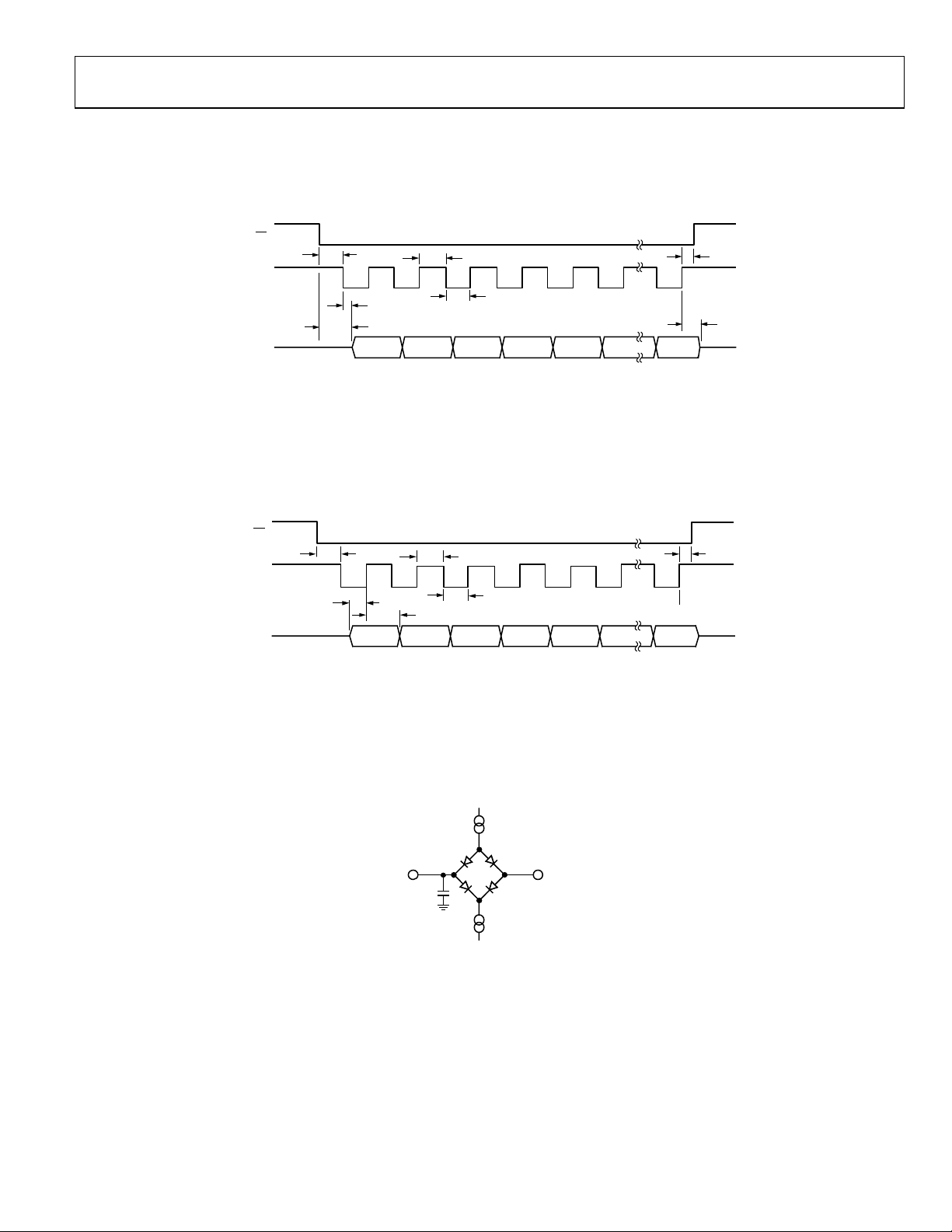
These numbers are measured with the load circuit of Figure 4 and defined as the time required for the output to cross the VOL or VOH limits.
3
This specification is relevant only if CS goes low while SCLK is low.
4
These numbers are derived from the measured time taken by the data output to change 0.5 V when loaded with the circuit of Figure 4. The measured number is then
extrapolated back to remove effects of charging or discharging the 50 pF capacitor. This means that the times quoted in the Timing Specifications are the true bus
relinquish times of the part and as such are independent of external bus loading capacitances.
Rev. 0 | Page 6 of 32
AD7739
S
T
CS
t
4
SCLK
t
5
t
5A
DOUT MSB LSB
t
6
t
7
Figure 2. Read Cycle Timing Diagram
CS
t
CLK
DIN
11
t
12
t
MSB
t
14
t
15
13
Figure 3. Write Cycle Timing Diagram
LSB
t
9
t
8
03742-0-002
t
16
03742-0-003
I
(800µA AT DVDD = 5V
SINK
O OUTPUT
PIN
50pF
100µA AT DV
I
(200µA AT DVDD = 5V
SOURCE
100µA AT DV
1.6V
DD
= 3V)
= 3V)
DD
03742-0-004
Figure 4. Load Circuit for Access Time and Bus Relinquish Time
Rev. 0 | Page 7 of 32

AD7739
ABSOLUTE MAXIMUM RATINGS
Table 3. (TA = 25°C, unless otherwise noted.)
Parameter Rating
AVDD to AGND, DVDD to DGND –0.3 V to +7 V
AGND to DGND –0.3 V to +0.3 V
AVDD to DVDD –5 V to +5 V
AIN, AINCOM to AGND –0.3 V to AVDD + 0.3 V
REFIN+, REFIN– to AGND –0.3 V to AVDD + 0.3 V
P0, P1 Voltage to AGND –0.3 V to AVDD + 0.3 V
Digital Input Voltage to DGND –0.3 V to DVDD + 0.3 V
Digital Output Voltage to DGND –0.3 V to DVDD + 0.3 V
ESD Rating (ESD Association Human Body Model, S5.1) 4000 V
Operating Temperature Range –40°C to +105°C
Storage Temperature Range –65°C to +150°C
Junction Temperature 150°C
TSSOP Package θJA Thermal Impedance
Lead Temperature, Soldering
Vapor Phase (60 sec) 215°C
Infrared (15 sec) 220°C
128°C/W
Stresses above those listed under Absolute Maximum Ratings may cause permanent damage to the device. This is a stress rating only;
functional operation of the device at these or any other conditions above those indicated in the operational section of this specification is
not implied. Exposure to absolute maximum rating conditions for extended periods may affect device reliability.
Rev. 0 | Page 8 of 32
AD7739
TYPICAL PERFORMANCE CHARACTERISTICS
25
24
23
22
21
20
19
NO MISSING CODES
18
17
16
5 6 7 8 9 101112131415
CHOP = 1
FILTER WORD
03742-0-005
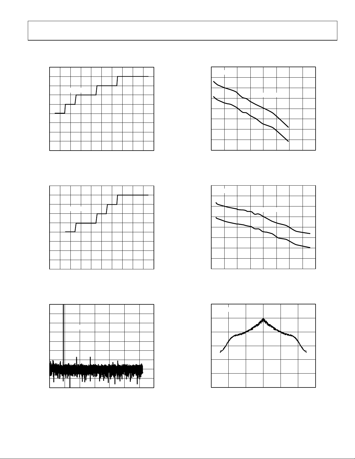
Figure 5. No Missing Codes Performance, Chopping Enabled
25
24
23
22
21
20
19
NO MISSING CODES
18
17
16
5 6 7 8 9 101112131415
CHOP = 0
FILTER WORD
03742-0-006
Figure 6. No Missing Codes Performance, Chopping Disabled
0
–20
–40
–60
–80
–100
GAIN (dB)
–120
–140
–160
–180
0 200 400 600 800 1000 1200 1400
THD = 110dB
INPUT FREQUENCY (Hz)
03742-0-007
Figure 7. Typical FFT Plot; Input Sine Wave 183 Hz,1.2 V Peak, AIN Range
±1.25 V, Conversion Time 397 µs, Chopping Enabled, MCLK = 6.144 MHz
24
CHOP = 1
22
20
18
16
14
RESOLUTION (bits)
12
10
8
EFFECTIVE (rms)
p-p
1068240 121416
OUTPUT DATA RATE (kHz)
03742-0-008
Figure 8. Typical Effective and Peak-to-Peak Resolution; AIN Voltage = 0 V,
AIN Range ±1.25 V, Chopping Enabled, MCLK = 6.144 MHz
24
CHOP = 0
22
20
18
16
14
RESOLUTION (bits)
12
10
8
EFFECTIVE (rms)
p-p
1068240 121416
OUTPUT DATA RATE (kHz)
03742-0-009
Figure 9. Typical Effective and Peak-to-Peak Resolution; AIN Voltage = 0 V,
AIN Range ±1.25 V, Chopping Disabled, MCLK = 6.144 MHz
120
CHOP = 1
110
100
90
CMR (dB)
80
70
60
AIN DIFFERENTIAL VOLTAGE (V)
0–0.5–1.0–1.5 0.5 1.0 1.5
03742-0-010
Figure 10. Typical Common-Mode Rejection vs. AIN Voltage; AIN Range
±1.25 V, Conversion Time 397 µs, Chopping Enabled, MCLK = 6.144 MHz
Rev. 0 | Page 9 of 32

AD7739
OUTPUT NOISE AND RESOLUTION SPECIFICATION
The AD7739 can be operated with chopping enabled or
disabled, allowing the ADC to be programmed to optimize
either the offset drift performance or the throughput rate and
channel switching time. Noise tables for these two primary
modes of operation are outlined below for a selection of output
rates and settling times.
The AD7739 noise performance depends on the selected
chopping mode, the filter word (FW) value, and the selected
analog input range. The AD7739 noise will not vary
significantly with MCLK frequency.
CHOPPING ENABLED
The first mode, in which the AD7739 is configured with
chopping enabled (CHOP = 1), provides very low noise with
lower output rates.
Table 4. Typical Output RMS Noise in µV vs. Conversion Time and Input Range with Chopping Enabled
Conversion
Time
Register
127 0xFF 2689 372 200 1.8 1.1
46 0xAE 1001 999 500 2.7 1.7
17 0x91 397 2519 1325 4.8 2.7
10 0x8A 251 3982 2209 9.3 4.7
9 0x89 230 4342 2450 10.8 6.3
2 0x82 84 11838 9500 600 460
Time
(µs)
Output Data
Rate
(Hz)
–3 dB
Frequency
(Hz)
Table 4 to Table 6 show the –3 dB frequencies and typical
performance versus the channel conversion time and equivalent
output data rate, respectively.
Table 4 shows the typical output rms noise. Table 5 shows the
typical effective resolution based on rms noise. Table 6 shows
the typical output peak-to-peak resolution, representing values
for which there will be no code flicker within a 6-sigma limit.
The peak-to-peak resolutions are not calculated based on rms
noise but on peak-to-peak noise.
These typical numbers are generated from 4096 data samples
acquired in continuous conversion mode with an analog input
voltage set to 0 V and MCLK = 6.144 MHz. The conversion
time is selected via the channel conversion time register.
Input Range / RMS Noise (µV) FW Conversion
±2.5 V, +2.5 V ±1.25 V, +1.25 V, ±0.625 V, +0.625 V
Table 5. Typical Effective Resolution in Bits vs. Conversion Time and Input Range with Chopping Enabled
Conversion
Time
Register
127 0xFF 2689 372 200 21.4 20.4 21.2 20.2 20.2 19.2
46 0xAE 1001 999 500 20.8 19.8 20.5 19.5 19.5 18.5
17 0x91 397 2519 1325 20.0 19.0 19.8 18.8 18.8 17.8
10 0x8A 251 3982 2209 19.0 18.0 19.0 18.0 18.0 17.0
9 0x89 230 4342 2450 18.8 17.8 18.6 17.6 17.6 16.6
2 0x82 84 11838 9500 12.9 11.9 12.4 11.4 11.4 10.4
Time
(µs)
Output Data
Rate
(Hz)
–3 dB
Frequency
(Hz)
±2.5 V +2.5 V ±1.25 V +1.25 V ±0.625 V +0.625 V
Input Range / Effective Resolution (Bits) FW Conversion
Table 6. Typical Peak-to-Peak Resolution in Bits vs. Conversion Time and Input Range with Chopping Enabled
Conversion
Time
Register
127 0xFF 2689 372 200 18.6 17.6 18.3 17.3 17.3 16.3
46 0xAE 1001 999 500 17.9 16.9 17.6 16.6 16.6 15.6
17 0x91 397 2519 1325 17.1 16.1 16.9 15.9 15.9 14.9
10 0x8A 251 3982 2209 16.2 15.2 16.2 15.2 15.2 14.2
9 0x89 230 4342 2450 16.0 15.0 15.8 14.8 14.8 13.8
2 0x82 84 11838 9500 10.7 9.7 9.7 8.7 8.7 7.7
Time
(µs)
Output Data
Rate
(Hz)
–3 dB
Frequency
(Hz)
Input Range / Peak-to-Peak Resolution (Bits) FW Conversion
±2.5 V +2.5 V ±1.25 V +1.25 V ±0.625 V +0.625 V
Rev. 0 | Page 10 of 32
 Loading...