LC2MOS
a
FEATURES
22-Bit Sigma-Delta ADC
Dynamic Range of 105 dB (146 Hz Input)
60.003% Integral Nonlinearity
On-Chip Low-Pass Digital Filter
Cutoff Programmable from 584 Hz to 36.5 Hz
Linear Phase Response
Five Line Serial I/O
Twos Complement Coding
Easy Interface to DSPs and Microcomputers
Software Control of Filter Cutoff
65 V Supply
Low Power Operation: 50 mW
APPLICATIONS
Biomedical Data Acquisition
ECG Machines
EEG Machines
Process Control
High Accuracy Instrumentation
Seismic Systems
22-Bit Data Acquisition System
AD7716
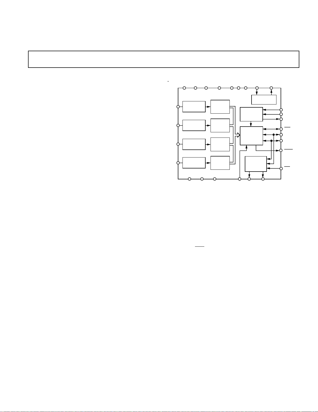
FUNCTIONAL BLOCK DIAGRAM
AIN1
AIN2
AIN3
AIN4
AV
DD
MODULATOR
MODULATOR
MODULATOR
MODULATOR
V
DV
DD
AD7716
ANALOG
ANALOG
ANALOG
ANALOG
REF
AV
RESET
SS
LOW PASS
DIGITAL
FILTER
LOW PASS
DIGITAL
FILTER
LOW PASS
DIGITAL
FILTER
LOW PASS
DIGITAL
FILTER
AGND DGND
A0 A1 A2
DIN1
GENERATION
CONTROL
LOGIC
OUTPUT
SHIFT
REGISTER
CONTROL
REGISTER
D
1
OUT
CLOCK
D
OUT
CLKOUTCLKIN
MODE
CASCIN
CASCOUT
RFS
SDATA
SCLK
DRDY
TFS
2
GENERAL DESCRIPTION
The AD7716 is a signal processing block for data acquisition
systems. It is capable of processing four channels with bandwidths of up to 584 Hz. Resolution is 22 bits and the usable
dynamic range varies from 111 dB with an input bandwidth of
36.5 Hz to 99 dB with an input bandwidth of 584 Hz.
The device consists of four separate A/D converter channels that
are implemented using sigma-delta technology. Sigma-delta
ADCs include on-chip digital filtering and, thus, the system
filtering requirements are eased.
Three address pins program the device address. This allows a
data acquisition system with up to 32 channels to be set up in a
simple fashion. The output word from the device contains 32
bits of data. One bit is determined by the state of the D
IN
1 input and may be used, for example, in an ECG system with an
external pacemaker detect circuit to indicate that the output
word is invalid because of the presence of a pacemaker pulse.
There are 22 bits of data corresponding to the analog input.
Two bits contain the channel address and 3 bits are the device
address. Thus, each channel in a 32-channel system would have
a discrete 5-bit address. The device also has a CASCOUT pin
and a CASCIN pin that allow simple networking of multiple
devices.
The on-chip control register is programmed using the SCLK,
SDATA and
TFS pins. Three bits of the Control Register set
the digital filter cutoff frequency for the device. Selectable frequencies are 584 Hz, 292 Hz, 146 Hz, 73 Hz and 36.5 Hz. A
further 2 bits appear as outputs D
OUT
1 and D
2 and can be
OUT
used for controlling calibration at the front end. The device is
available in a 44-pin PQFP (Plastic Quad Flatpack) and 44-pin
PLCC.
REV. A
Information furnished by Analog Devices is believed to be accurate and
reliable. However, no responsibility is assumed by Analog Devices for its
use, nor for any infringements of patents or other rights of third parties
which may result from its use. No license is granted by implication or
otherwise under any patent or patent rights of Analog Devices.
One Technology Way, P.O. Box 9106, Norwood, MA 02062-9106, U.S.A.
Tel: 617/329-4700 Fax: 617/326-8703

AD7716–SPECIFICATIONS
6 5%; AVSS = –5 V 6 5%; AGND = DGND = 0 V; V
Resistance = 750 V2 with 1 nF to AGND at each AIN. TA = T
= 2.5 V; Filter Cutoff = 146 Hz; Noise Measurement Bandwidth = 146 Hz; AIN Source
REF
MIN
= 8 MHz; MODE Pin Is High (Slave Mode Operation); AVDD = DV
CLKIN
to T
, unless otherwise noted.)
MAX
= +5 V
DD
1, 2
(f
Parameter B Version Units Test Conditions/Comments
STATIC PERFORMANCE
Resolution 22 Bits
Integral Linearity Error 0.003 % FSR typ Guaranteed No Missed Codes to 21 Bits
3
0.006 % FSR max
Gain Error 1 % FSR max
Gain Match Between Channels 0.5 % FSR max
Gain TC 30 µV/°C typ
Offset Error 0.2 % FSR max
Offset Match Between Channels 0.1 % FSR max
Offset TC 4 µV/°C typ
Noise 11 µV rms max See Table I for Typical Noise Performance vs. Programmed
Cutoff Frequency
DYNAMIC PERFORMANCE
Sampling Rate f
Output Update Rate f
Filter Cutoff Frequency f
Settling Time (3 3 14 3 256 3 2N/f
Usable Dynamic Range
4
/14 570 kHz for f
CLKIN
/(14 3 256 3 2N) N Is Decimal Equivalent of FC2, FC1, FC0 in Control Register
CLKIN
/(3.81 3 14 3 256 3 2N)
CLKIN
CLKIN
)
CLKIN
= 8 MHz
See Table I
Total Harmonic Distortion –90 dB typ Input Frequency = 35 Hz
Absolute Group Delay
3
Differential Group Delay
3
–100 dB typ AIN = ±10 mV p-p
(3 3 14 3 256 3 2N)/2f
CLKIN
10 ns typ
Channel-to-Channel Isolation –85 dB typ Feedthrough from Any One Channel to the Other Three, with
35 Hz Full-Scale Sine Wave Applied to that Channel
ANALOG INPUT
Input Range ± 2.5 Volts
Input Capacitance 10 pF typ
Input Bias Current 1 nA typ
LOGIC INPUTS
V
, Input High Voltage 2.4 V min
INH
V
, Input Low Voltage 0.8 V max
INL
IIN, Input Current
SDATA, RFS +10/-130 µA max Internal 50 kΩ Pull-Up Resistors
TFS +10/-650 µA max Internal 10 kΩ Pull-Up Resistor
All Other Inputs ±10 µA max
CIN, Input Capacitance
3
10 pF max
LOGIC OUTPUTS
VOH, Output High Voltage 2.4 V min |I
VOL, Output Low Voltage 0.4 V max |I
| ≤ 40 µA
OUT
| ≤ 1.6 mA
OUT
POWER SUPPLIES
Reference Input 2.4/2.6 V min/V max
AV
DD
DV
DD
AV
SS
I
DD
I
SS
Power Consumption 50 mW max 35 mW typ
Power Supply Rejection
NOTES
1
Operating temperature ranges as follows : B Version; –40°C to +85°C.
2
The AIN pins present a very high impedance dynamic load which varies with clock frequency.
3
Guaranteed by design and characterization. Digital filter has linear phase.
4
Usable dynamic range is guaranteed by measuring noise and relating this to the full-scale input range.
5
100 mV p-p, 120 Hz sine wave applied to each supply.
Specifications subject to change without notice.
5
4.75/5.25 V min/V max
4.75/5.25 V min/V max
–4.75/–5.25 V min/V max
7.5 mA max 4.8 mA typ
2.5 mA max 1.8 mA typ
–70 dB typ
REV. A–2–

AD7716
Table I. Typical Usable Dynamic Range, RMS Noise and Filter Settling Time vs. Filter Cutoff Frequency
Programmed Cutoff Output Update Usable Dynamic RMS Noise Filter Settling Time to Absolute Group
N Frequency (Hz) Rate (Hz) Range (dB) (mV) 60.0007% FS (ms) Delay (ms)
0 584 2232 99 21 1.35 0.675
1 292 1116 102 14 2.7 1.35
2 146 558 105 10 5.4 2.7
3 73 279 108 7 10.8 5.4
4 36.5 140 111 5 21.6 10.8
NOTE
Usable Dynamic Range is defined as the ratio of the rms full-scale reading (sine wave input) to the rms noise of the converter.
CONTROL REGISTER TIMING CHARACTERISTICS
DGND = 0 V; f
= 8 MHz; Input Levels: Logic 0 = 0 V, Logic 1 = DVDD; unless otherwise noted)
CLKIN
Limit at T
MIN
, T
MAX
1, 2
(AV
DD
= DV
= +5 V 6 5%; AVSS= –5 V 6 5%; AGND =
DD
Parameter (B Version) Units Conditions/Comments
t
1
t
2
t
3
t
4
t
5
t
6
NOTES
1
Sample tested at +25°C to ensure compliance. All input signals are specified with tr = tf = 5 ns (10% to 90% of 5 V) and timed from a voltage level of 1.6 V.
2
See Figure 2.
3
CLKIN Duty Cycle range is 40% to 60%.
1/f
CLKIN
77 ns min SCLK Width
30 ns min TFS Setup Time
20 ns min SDATA Setup Time
10 ns min SDATA Hold Time
20 ns min TFS Hold Time
1.6mA
TO
OUTPUT
PIN
C
L
50pF
200µA
ns min SCLK Period
I
OL
+2.1V
I
OH
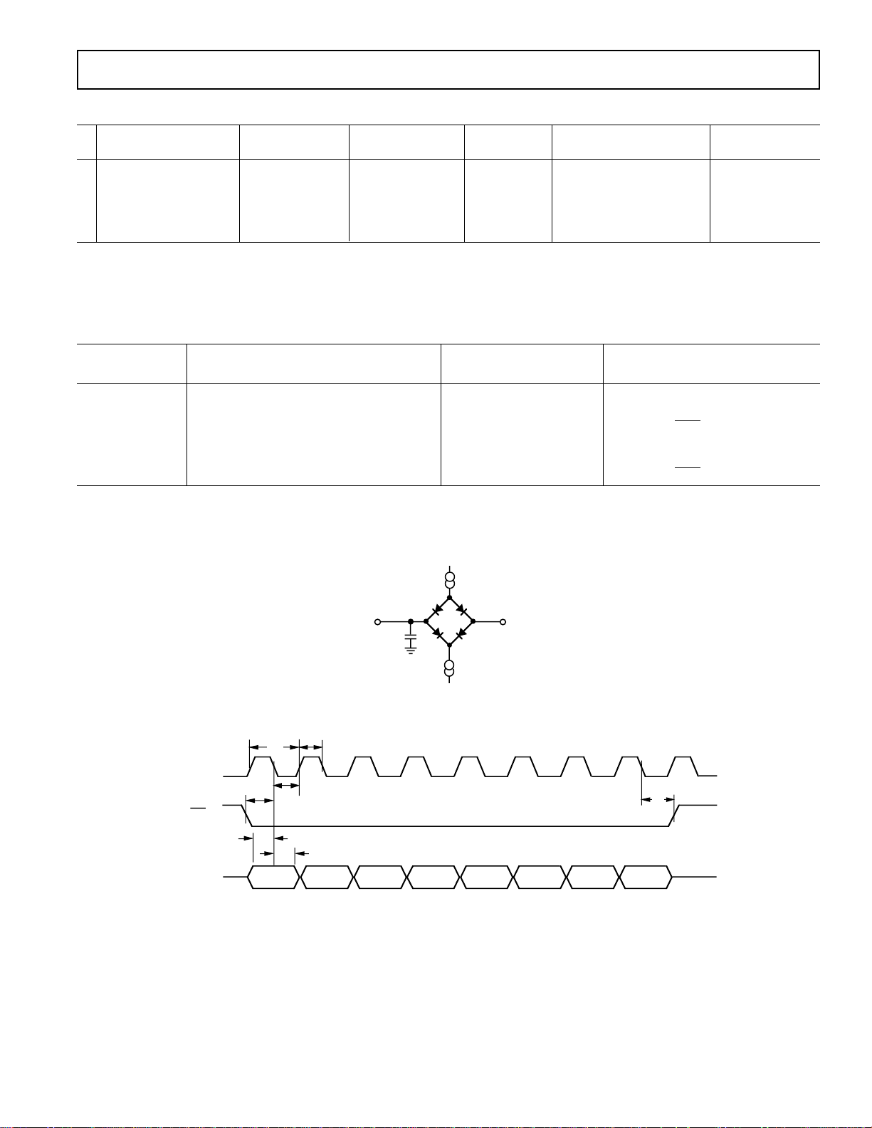
Figure 1. Load Circuit for Access Time and Bus Relinquish Time
REV. A
SCLK (I)
TFS (I)
SDATA (I)
t
3
t
4
(DB8)
t
DB0
t
2
1
t
2
t
5
DB1
(DB9)
DB2
(DB10)
DB3
(DB11)
DB4
(DB12)
DB5
(DB13)
DB6
(DB14)
DB7
(DB15)
t
6
Figure 2. Control Register Timing Diagram
–3–

AD7716
1, 2
MASTER MODE TIMING CHARACTERISTICS
f
= 8 MHz; Input Levels: Logic 0 = 0 V, Logic 1 = DVDD; unless otherwise noted)
CLKIN
Limit at T
MIN
, T
MAX
(AVDD = DV
Parameter (B Version) Units Conditions/Comments
f
CLKIN
5
t
r
5
t
f
t
7
t
8
t
9
t
10
t
11
t
12
t
13
t
14
t
15
6
t
16
7
t
17
t
18
t
19
3, 4
400 kHz min CLKIN Frequency
8 MHz max
40 ns max Digital Output Rise Time. Typically 20 ns
40 ns max Digital Output Fall Time. Typically 20 ns
1/f
1/f
1/2f
CLKIN
CLKIN
+ 30 ns max DRDY Low to SCLK Low Delay
CLKIN
ns min CASCIN Pulse Width
ns min CASCIN to DRDY Setup Time
50 ns max CLKIN High to DRDY Low, SCLK Active, RFS Active
40 ns max CLKIN High to SCLK High Delay
50 ns min SCLK Width
1/f
CLKIN
ns SCLK Period
40 ns max SCLK High to RFS High Delay
1/f
CLKIN
ns RFS Pulse Width
45 ns max SCLK High to SDATA Valid Delay
1/2f
1/2f
1/2f
+ 50 ns max SCLK Low to SDATA High Impedance Delay
CLKIN
+ 10 ns min
CLKIN
+ 60 ns max CLKIN High to DRDY High Delay
CLKIN
50 ns max CLKIN High to RFS High Impedance, SCLK High Impedance
20 ns min
t
20
t
21
NOTES
1
Sample tested at +25°C to ensure compliance. All input signals are specified with tr = tf = 5 ns (10% to 90% of 5 V) and timed from a voltage level of 1.6 V.
2
See Figures 1 and 3.
3
CLKIN duty cycle range is 40% to 60%.
4
The AD7716 is production tested with f
5
Specified using 10% and 90% points on waveform of interest.
6
t
is measured with the load circuit of Figure 1 and defined as the time required for an output to cross 0.8 V or 2.4 V.
16
7
t
is derived from the measured time taken by the data outputs to change 0.5 V when loaded with the circuit of Figure 1. The measured number is then extrapolated
17
back to remove the effects of charging or discharging the 100 pF capacitor. This means that the time quoted in the timing characteristics is the true bus relinquish
1/2f
2/f
time of the part and as such is independent of external bus loading capacitances.
+ 50 ns max SCLK Low to CASCOUT High Delay
CLKIN
CLKIN
at 8 MHz in the slave mode. It is guaranteed by characterization to operate at 400 kHz and 8 MHz in master mode.
CLKIN
ns CASCOUT Pulse Width
= +5 V 6 5%; AVSS= –5 V 6 5%; AGND = DGND = 0 V;
DD
CASCIN (I)
CLKIN (I)
DRDY (O)
SCLK (O)
RFS (O)
SDATA (O)
CASCOUT (O)
t
7
t
8
t
9
t
10
t
16
DB31
CH1
t
11
t
DB30
CH1
t
12
12
DB29
CH1
t
14
DB25
CH1
t
13
t
15
DB24
DB23
CH1
CH1
DB2
CH4
DB1
CH4
DB0
CH4
t
18
t
19
t
19
t
17
t
21
t
20
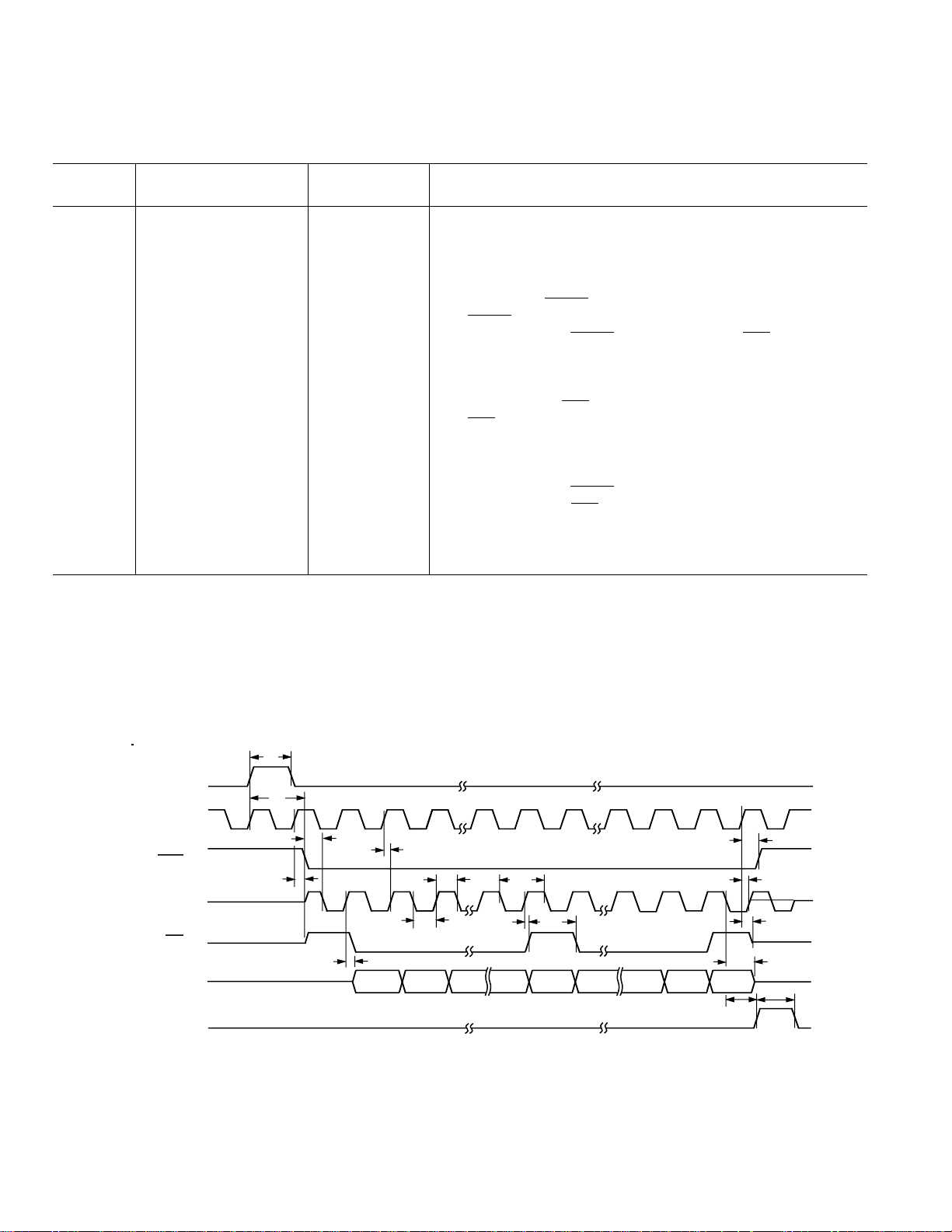
Figure 3. Master Mode Timing Diagram
–4–
REV. A

AD7716
1, 2
(AV
= DV
SLAVE MODE TIMING CHARACTERISTICS
f
= 8 MHz; Input Levels: Logic 0 = 0 V, Logic 1 = DVDD; unless otherwise noted)
CLKIN
DD
Parameter (B Version) Units Conditions/Comments
f
CLKIN
5
t
r
5
t
f
t
23
t
24
t
25
t
26
t
27
6
t
28
t
29
7
t
30
3, 4
400 kHz min CLKIN Frequency
8 MHz max
40 ns max Digital Output Rise Time. Typically 20 ns
40 ns max Digital Output Fall Time. Typically 20 ns
1/f
CLKIN
ns min CASCIN Pulse Width
50 ns min SCLK Width
125 ns min SCLK Period
1/f
+30 ns min CASCIN High to RFS Setup Time
CLKIN
30 ns min RFS Low to SCLK High Setup Time
50 ns max SCLK High to SDATA Valid Delay
50 ns min RFS Hold Time After SCLK High
50 ns max SCLK High to SDATA High Impedance Delay
0 ns min
t
31
t
32
NOTES
1
Sample tested at +25°C to ensure compliance. All input signals are specified with tr = tf = 5 ns (10% to 90% of 5 V) and timed from a voltage level of 1.6 V.
2
See Figures 1 and 4.
3
CLKIN duty cycle range is 40% to 60%.
4
The AD7716 is production tested with f
5
Specified using 10% and 90% points on waveform of interest.
6
t28 is measured with the load circuit of Figure 1 and defined as the time required for an output to cross 0.8 V or 2.4 V.
7
t30 is derived from the measured time taken by the data outputs to change 0.5 V when loaded with the circuit of Figure 1. The measured number is then extrapolated
back to remove the effects of charging or discharging the 100 pF capacitor. This means that the time quoted in the timing characteristics is the true bus relinquish
time of the part and as such is independent of external bus loading capacitances.
60 ns max SCLK High to CASCOUT High Delay.
2/f
CLKIN
at 8 MHz in the slave mode. It is guaranteed by characterization to operate at 400 kHz.
CLKIN
ns max CASCOUT Pulse Width
= +5 V 6 5%; AVSS= –5 V 6 5%; AGND = DGND = 0 V;
DD
CASCIN (I)
SCLK (I)
RFS (I)
SDATA (O)
CASCOUT (O)
t
23
t
24
t
26
t
28
t
27
DB31
CH1
t
24
DB30
CH1
t
25
DB29
CH1
DB28
CH1
DB27
CH1
DB2
CH4
t
DB1
CH4
31
DB0
CH4
t
t
29
t
30
32
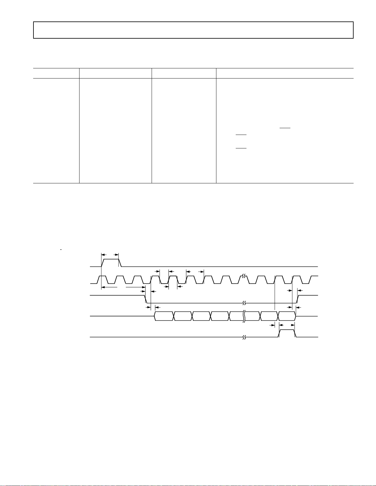
Figure 4. Slave Mode Timing Diagram
REV. A
–5–
 Loading...