

615 V Operation
a
FEATURES
128 Position
Potentiometer Replacement
10 kV, 50 kV, 100 kV, 1 MV
Power Shutdown: Less than 1 mA
3-Wire SPI Compatible Serial Data Input
+5 V to +30 V Single Supply Operation
65 V to 615 V Dual Supply Operation
Midscale Preset
APPLICATIONS
Mechanical Potentiometer Replacement
Instrumentation: Gain, Offset Adjustment
Programmable Voltage-to-Current Conversion
Programmable Filters, Delays, Time Constants
Line Impedance Matching
Power Supply Adjustment
GENERAL DESCRIPTION
The AD7376 provides a single channel, 128-position digitallycontrolled variable resistor (VR) device. This device performs the
same electronic adjustment function as a potentiometer or variable resistor. These products were optimized for instrument and
test equipment applications where a combination of high voltage
with a choice between bandwidth or power dissipation are available as a result of the wide selection of end-to-end terminal resistance values. The AD7376 contains a fixed resistor with a wiper
contact that taps the fixed resistor value at a point determined by
a digital code loaded into the SPI-compatible serial-input register. The resistance between the wiper and either endpoint of the
fixed resistor varies linearly with respect to the digital code transferred into the VR latch. The variable resistor offers a completely
programmable value of resistance between the A terminal and the
wiper or the B terminal and the wiper. The fixed A to B terminal
resistance of 10 kΩ, 50 kΩ, 100 kΩ or 1 MΩ has a nominal temperature coefficient of –300 ppm/°C.
The VR has its own VR latch which holds its programmed resistance value. The VR latch is updated from an internal serial-toparallel shift register which is loaded from a standard 3-wire
serial-input digital interface. Seven data bits make up the data
word clocked into the serial data input register (SDI). Only the
last seven bits of the data word loaded are transferred into the
7-bit VR latch when the CS strobe is returned to logic high. A
serial data output pin (SDO) at the opposite end of the serial
register allows simple daisy-chaining in multiple VR applications
without additional external decoding logic.
The reset (RS) pin forces the wiper to the midscale position by
loading 40
*Patent Number: 5495245
into the VR latch. The SHDN pin forces the resistor
H
Digital Potentiometer
AD7376*
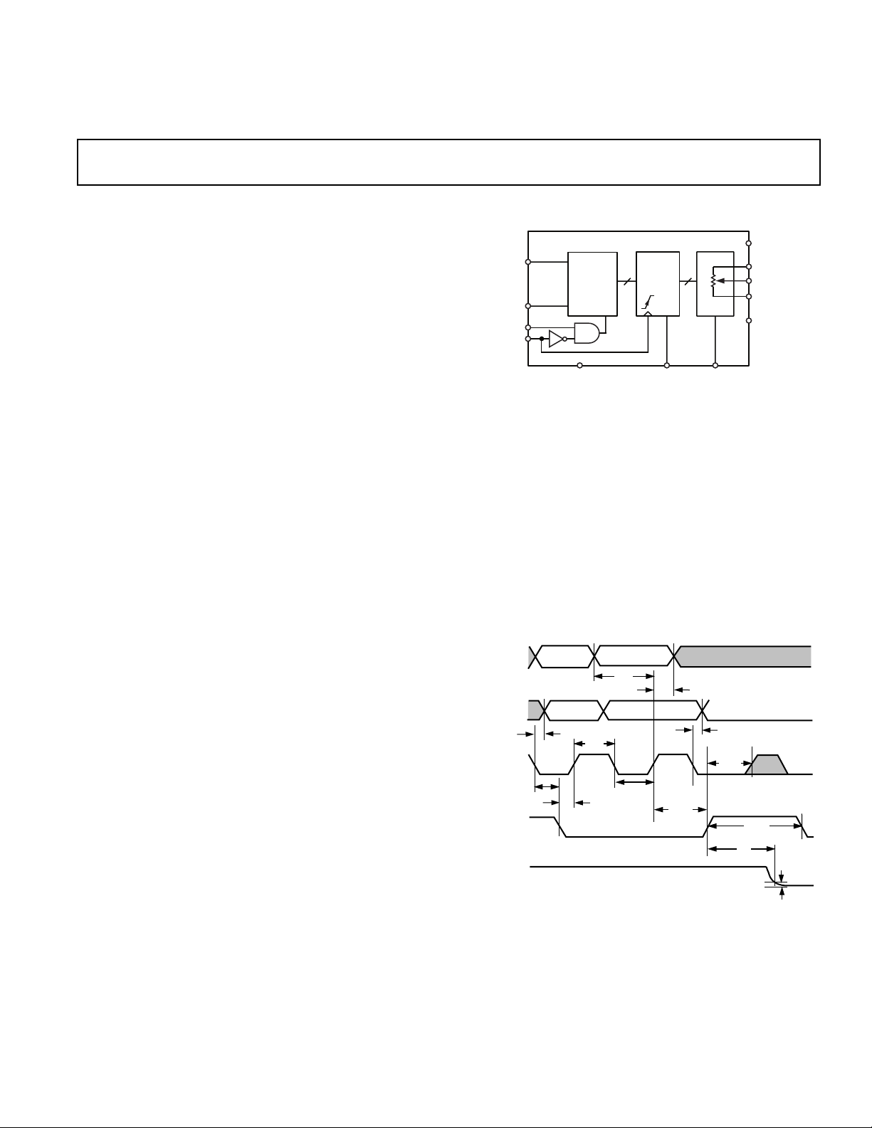
FUNCTIONAL BLOCK DIAGRAM
AD7376
SDO
SDI
CLK
CS
Q
7-BIT
SERIAL
REGISTER
D
CK
GND
7
7-BIT
LATCH
RS
7
R
SHDN
SHDN
to an end-to-end open circuit condition on the A terminal and
shorts the wiper to the B terminal, achieving a microwatt power
shutdown state. When shutdown is returned to logic high, the
previous latch settings put the wiper in the same resistance
setting prior to shutdown as long as power to V
moved. The digital interface is still active in shutdown so that
code changes can be made that will produce a new wiper position when the device is taken out of shutdown.
The AD7376 is available in both surface mount (SOL-16) and
the 14-lead plastic DIP package. For ultracompact solutions
selected models are available in the thin TSSOP package. All
parts are guaranteed to operate over the extended industrial
temperature range of –40°C to +85°C. For operation at lower
supply voltages (+3 V to +5 V), see the AD8400/AD8402/
AD8403 products.
1
SDI
(DATA IN)
SDO
(DATA OUT)
CLK
CS
V
OUT
t
V
0
1
0
1
0
CSH0
1
0
DD
0V
D
X
t
D'
X
t
CH
t
CSS
D
X
DS
t
DH
D'
X
t
CL
t
CSH
61 LSB ERROR BAND
Figure 1. Detail Timing Diagram
The last seven data bits clocked into the serial input register will
be transferred to the VR 7-bit latch when CS returns to logic
high. Extra data bits are ignored.
is not re-
DD
t
PD_MAX
t
CS1
t
t
S
V
A
W
B
V
CSW
DD
SS
61 LSB
REV. 0
Information furnished by Analog Devices is believed to be accurate and
reliable. However, no responsibility is assumed by Analog Devices for its
use, nor for any infringements of patents or other rights of third parties
which may result from its use. No license is granted by implication or
otherwise under any patent or patent rights of Analog Devices.
One Technology Way, P.O. Box 9106, Norwood, MA 02062-9106, U.S.A.
Tel: 781/329-4700 World Wide Web Site: http://www.analog.com
Fax: 781/326-8703 © Analog Devices, Inc., 1997

AD7376–SPECIFICA TIONS
(VDD/VSS = 615 V 6 10% or 6 5 V 6 10%, VA = +VDD, VB = VSS/0 V, –408C < TA < +858C
ELECTRICAL CHARACTERISTICS
Parameter Symbol Conditions Min Typ1Max Units
DC CHARACTERISTICS RHEOSTAT MODE (Specifications Apply to All VRs)
Resistor Differential NL
Resistor Nonlinearity
Nominal Resistor Tolerance ∆RT
Resistance Temperature Coefficient R
Wiper Resistance R
Wiper Resistance R
DC CHARACTERISTICS POTENTIOMETER DIVIDER MODE (Specifications Apply to All VRs)
Resolution N 7 Bits
Integral Nonlinearity
Differential Nonlinearity
Voltage Divider Temperature Coefficient ∆V
Full-Scale Error V
Zero-Scale Error V
RESISTOR TERMINALS
Voltage Range
Capacitance
Capacitance
4
5
A, B C
5
WC
Shutdown Supply Current
Shutdown Wiper Resistance R
Common-Mode Leakage I
DIGITAL INPUTS AND OUTPUTS
Input Logic High V
Input Logic Low V
Output Logic High V
Output Logic Low
Input Current I
Input Capacitance
POWER SUPPLIES
Power Supply Range V
Power Supply Range V
Supply Current I
Supply Current I
Supply Current I
Power Dissipation
Power Supply Sensitivity PSS ∆V
DYNAMIC CHARACTERISTICS
Bandwidth –3 dB BW_10K RAB = 10 kΩ, Code = 40
Bandwidth –3 dB BW_50K R
Bandwidth –3 dB BW_100K R
Total Harmonic Distortion THD
V
Settling Time t
W
Resistor Noise Voltage e
INTERFACE TIMING CHARACTERISTICS (Applies to All Parts [Notes 5, 11])
Input Clock Pulsewidth t
Data Setup Time t
Data Hold Time t
CLK to SDO Propagation Delay
CS Setup Time t
CS High Pulsewidth t
Reset Pulsewidth t
CLK Rise to CS Rise Hold Time t
CS Rise to Clock Rise Setup t
2
2
3
3
6
7
5
8
5, 9, 10
12
unless otherwise noted.)
R-DNL RWB, VA = NC –1 ±0.25 +1 LSB
R-INL RWB, VA = NC –1 ±0.5 +1 LSB
= +25°C –30 30 %
/∆TVAB = VDD, Wiper = No Connect –300 ppm/°C
AB
W
W
INL –1 ±0.5 +1 LSB
DNL –1 ±0.1 +1 LSB
/∆T Code = 40
W
WFSE
WZSE
V
A, B, W
A, B
W
I
A_SD
W_SD
CM
IH
IL
OH
V
OL
IL
C
IL
DD/VSS
DD
DD
DD
SS
P
DISS
PSS ∆VDD = +15 V ± 10% or ∆VSS = –15 V ± 10% 0.01 0.02 %/%
W
S
N_WB
, t
CH
CL
DS
DH
t
PD
CSS
CSW
RS
CSH
CS1
A
IW = ±15 V/R
IW = ±5 V/R
Code = 7F
Code = 00
f = 1 MHz, Measured to GND, Code = 40
f = 1 MHz, Measured to GND, Code = 40
NOMINAL
NOMINAL
H
H
H
H
H
120 200 Ω
200 Ω
5 ppm/°C
–2 –0.5 +0 LSB
0 +0.5 +1 LSB
V
SS
V
V
DD
45 pF
60 pF
VA = VDD, VB = 0 V, SHDN = 0 0.01 1 µA
VA = VDD, VB = 0 V, SHDN = 0, VDD = +15 V 170 400 Ω
VA = VB = V
W
1nA
VDD = +5 V or +15 V 2.4 V
VDD = +5 V or +15 V 0.8 V
RL = 2.2 kΩ to +5 V 4.9 V
IOL = 1.6 mA, V
= +5 V, VDD = +15 V 0.4 V
LOGIC
VIN = 0 V or +15 V ±1 µA
5pF
Dual Supply Range ±4.5 ±16.5 V
Single Supply Range, VSS = 0 4.5 28 V
VIH = +5 V or VIL = 0 V, VDD = +5 V 0.0001 0.01 mA
VIH = +5 V or VIL = 0 V, VDD = +15 V 0.75 2 mA
VIH = +5 V or VIL = 0 V, VSS = –5 V or –15 V 0.02 0.1 mA
VIH = +5 V or VIL = 0 V, VDD = +15 V, VSS = –15 V 11 30 mW
= +5 V ± 10%, or ∆VSS = –5 V ± 10% 0.05 0.15 %/%
DD
520 kHz
125 kHz
60 kHz
= 50 kΩ, Code = 40
AB
= 100 kΩ, Code = 40
AB
H
H
H
VA = 1 V rms, VB = 0 V, f = 1 kHz 0.005 %
VA = 10 V, VB = 0 V, ±1 LSB Error Band 4 µs
RWB = 25 kΩ, f = 1 kHz, RS = 0 14 nV√Hz
Clock Level High or Low 120 ns
30 ns
20 ns
RL = 2.2 kΩ, CL < 20 pF 10 100 ns
120 ns
150 ns
120 ns
120 ns
120 ns
–2–
REV. 0
AD7376
WARNING!
ESD SENSITIVE DEVICE
NOTES
11
Typicals represent average readings at +25°C, VDD = +15 V, and VSS = –15 V.
12
Resistor position nonlinearity error R-INL is the deviation from an ideal value measured between the maximum resistance and the minimum resistance wiper positions. R-DNL measures the relative step change from ideal between successive tap positions. Parts are guaranteed monotonic. See Figure 27. Test Circuit.
13
INL and DNL are measured at VW with the RDAC configured as a potentiometer divider similar to a voltage output D/A converter. VA = VDD and VB = 0 V. DNL
specification limits of ±1 LSB maximum are Guaranteed Monotonic operating conditions. See Figure 26. Test Circuit.
14
Resistor terminals A, B, W have no limitations on polarity with respect to each other.
15
Guaranteed by design and not subject to production test.
16
Measured at the A terminal. A terminal is open circuit in shutdown mode.
17
IOL = 200 µA for the 50 kΩ version operating at VDD = +5 V.
18
P
is calculated from (IDD × VDD). CMOS logic level inputs result in minimum power dissipation.
DISS
19
Bandwidth, noise and settling time are dependent on the terminal resistance value chosen. The lowest R value results in the fastest settling time and highest bandwidth. The highest R value results in the minimum overall power consumption.
10
All dynamic characteristics use VDD = +15 V and VSS = –15 V.
11
See timing diagram for location of measured values. All input control voltages are specified with tR = tF = 1 ns (10% to 90% of VDD) and timed from a voltage level
of 1.6 V. Switching characteristics are measured using both VDD = +5 V or +15 V.
12
Propagation delay depends on value of VDD, RL and CL see Applications section.
Specifications subject to change without notice.
ABSOLUTE MAXIMUM RATINGS
(TA = +25°C, unless otherwise noted)
VDD to GND . . . . . . . . . . . . . . . . . . . . . . . . . . .–0.3 V, +30 V
V
to GND . . . . . . . . . . . . . . . . . . . . . . . . . . +0.3 V, –16.5 V
SS
V
to VSS . . . . . . . . . . . . . . . . . . . . . . . . . . . .–0.3 V, +44 V
DD
V
, VB, VW to GND . . . . . . . . . . . . . . . . . . . . . . . . . .VSS, V
A
DD
AX – BX, AX – WX, BX – WX . . . . . . . . . . . . . . . . . . . ±20 mA
Digital Input Voltages to GND . . . . . . . . . . 0 V, V
+ 0.3 V
DD
Digital Output Voltage to GND . . . . . . . . . . . . . . 0 V, +30 V
Operating Temperature Range . . . . . . . . . . . –40°C to +85°C
Maximum Junction Temperature (T
MAX) . . . . . . .+150°C
J
Storage Temperature . . . . . . . . . . . . . . . . . . –65°C to +150°C
Lead Temperature (Soldering, 10 sec) . . . . . . . . . . . .+300°C
Package Power Dissipation . . . . . . . . . . . . (T
Thermal Resistance θ
JA
MAX – TA)/θ
J
JA
P-DIP (N-14) . . . . . . . . . . . . . . . . . . . . . . . . . . . . 92°C/W
SOIC (SOL-16) . . . . . . . . . . . . . . . . . . . . . . . . . . 120°C/W
TSSOP-14 . . . . . . . . . . . . . . . . . . . . . . . . . . . . . . 240°C/W
ORDERING GUIDE
Temperature Package Package
Model kV Range Description Options
AD7376AN10 10 –40°C to +85°C PDIP-14 N-14
AD7376AR10 10 –40°C to +85°C SOL-16 R-16
AD7376ARU10 10 –40°C to +85°C TSSOP-14 RU-14
AD7376AN50 50 –40°C to +85°C PDIP-14 N-14
AD7376AR50 50 –40°C to +85°C SOL-16 R-16
AD7376ARU50 50 –40°C to +85°C TSSOP-14 RU-14
AD7376AN100 100 –40°C to +85°C PDIP-14 N-14
AD7376AR100 100 –40°C to +85°C SOL-16 R-16
AD7376ARU100 100 –40°C to +85°C TSSOP-14 RU-14
AD7376AN1M 1,000 –40°C to +85°C PDIP-14 N-14
AD7376AR1M 1,000 –40°C to +85°C SOL-16 R-16
AD7376ARU1M 1,000 –40°C to +85°C TSSOP-14 RU-14
Die Size: 101.6 mil × 127.6 mil, 2.58 mm × 3.24 mm
Number Transistors: 840
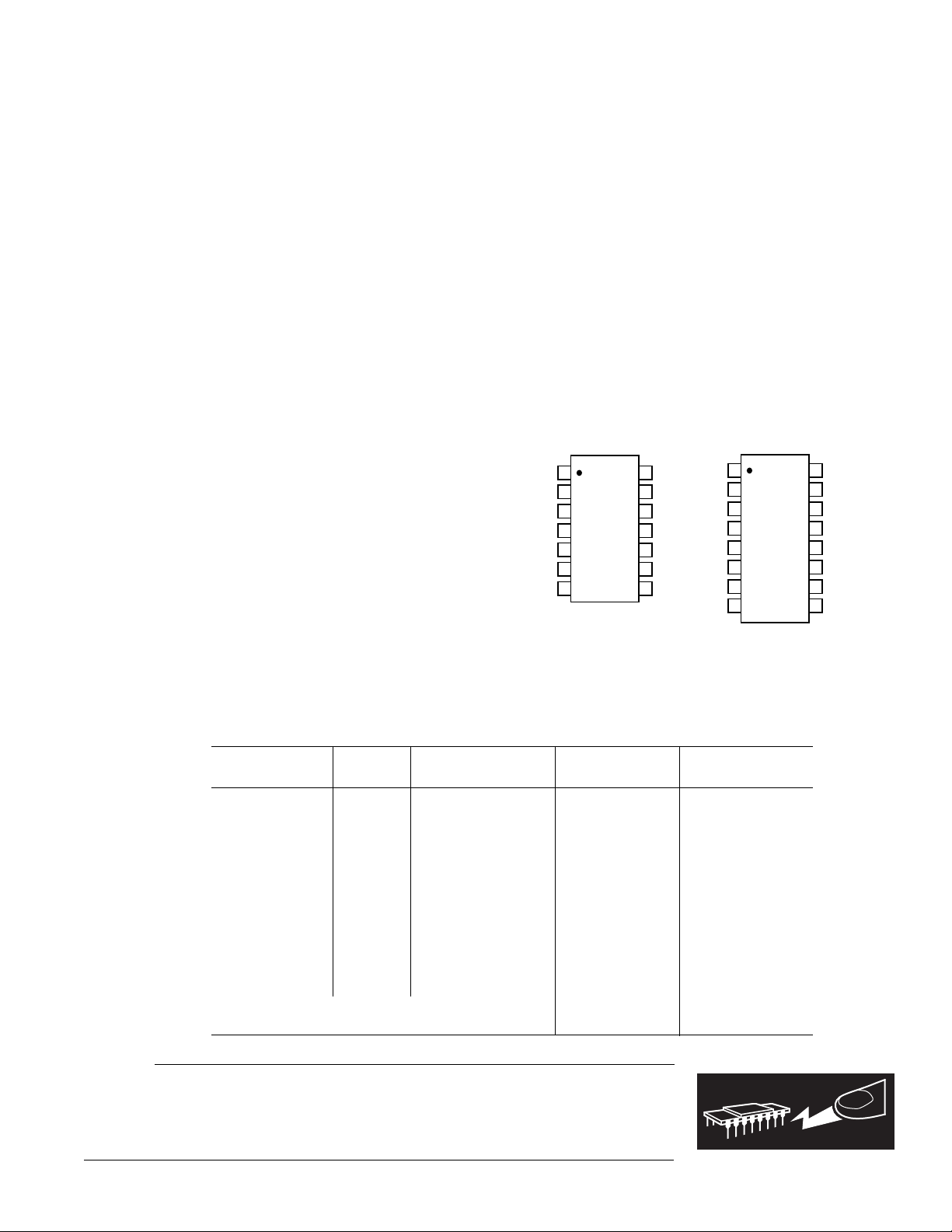
PIN CONFIGURATIONS
PDIP & TSSOP-14 SOL-16
1
A
1
B
2
V
3
SS
4
GND
CLK
TOP VIEW
(Not to Scale)
5
CS
6
RS
7
NC = NO CONNECT
AD7376
14
W
13
NC
12
V
DD
11
SDO
10
SHDN
SDI
9
8
NC
A
2
B
3
V
SS
4
GND
5
CS
(Not to Scale)
6
RS
CLK
7
8
NC
NC = NO CONNECT
AD7376
TOP VIEW
16
15
14
13
12
11
10
9
W
NC
V
DD
SDO
SHDN
SDI
NC
NC
CAUTION
ESD (electrostatic discharge) sensitive device. Electrostatic charges as high as 4000 V readily
accumulate on the human body and test equipment and can discharge without detection.
Although the AD7376 features proprietary ESD protection circuitry, permanent damage may
occur on devices subjected to high energy electrostatic discharges. Therefore, proper ESD
precautions are recommended to avoid performance degradation or loss of functionality.
–3–REV. 0
AD7376
CODE – Decimal
R-DNL ERROR – LSB
0.25
–0.25
0 16 12832 48 64 80 96 112
0.20
0.05
0
–0.10
–0.20
0.15
0.10
–0.05
–0.15
TA = –558C
TA = +258C
VDD = +15V
V
SS
= –15V
R
AB
= 50kV
TA = +858C
100
AB
75
50
PERCENT OF NOMINAL
25
END-TO-END RESISTANCE – % R
–Typical Performance Characteristics
R
WB
0
0
32 128
64 96
CODE – Decimal
R
Figure 2. Wiper To End Terminal
Percent Resistance vs. Code
WA
0.5
0.4
0.3
0.2
0.1
0
–0.1
–0.2
R-INL ERROR – LSB
–0.3
–0.4
–0.5
0 16 128
TA = –558C
TA = +258C
TA = +858C
VDD = +15V
= –15V
V
SS
V
= 2.5V
A
= 0V
V
B
= 50kV
R
AB
32 48 64 80 96 112
CODE – Decimal
Figure 3. Resistance Step Position
Nonlinearity Error vs. Code
Figure 4. Relative Resistance Step
Change from Ideal vs. Code
50
49
48
47
46
NOMINAL END-TO-END RESISTANCE – kV
45
–55 –35 105
VDD = +15V
V
R
–15 5 25 45 65 85
TEMPERATURE – 8C
Figure 5. Nominal Resistance vs.
Temperature
1.0
0.8
0.6
INL – LSB
0.4
0.2
0
51015202530
SUPPLY VOLTAGE (VDD - VSS) – Volts
Figure 8. Potentiometer Divider
Nonlinearity Error vs. Supply
Voltage
= –15V
SS
= 50kV NOMINAL
AB
VA = 2.5V
V
= 0V
B
CODE = 40
RAB = 50kV
14
01
125
H
12
10
8
– V
WA
V
6
4
2
0
0 0.25 20.5 0.75 1 1.25 1.5 1.75
10
H
20
H
40
H
CODE = 70
IWA – mA
H
TA = +258C
V
= +15V
DD
V
= –15V
SS
R
= 50kV
AB
7F
H
Figure 6. Resistance Linearity vs.
Conduction Current
20
15
H
10
5
0
–5
–10
/DT POTENTIOMETER
–15
WB
MODE TEMPCO – ppm/8C
–20
DV
–25
–30
0 16 128
32 48 64 80 96 112
VDD = +15V
V
= –15V
SS
V
= +2.5V
A
V
= 0V
B
–558C < T
R
= 50kV
AB
CODE – Decimal
< +858C
A
Figure 9. ∆VWB/∆T Potentiometer
Mode Tempco
–4–
1.5
1.2
0.9
R_INL – LSB
0.6
0.3
0
51015202530
SUPPLY VOLTAGE (VDD - VSS) – Volts
Iw = 100mA, TA = +258C
DATA = 40
H
Figure 7. Resistance Nonlinearity
Error vs. Supply Voltage
1000
900
RAB = 50kV
800
700
600
500
400
VDD = +5V
300
V
200
100
WIPER CONTACT RESISTANCE – V
0
–55 –35 125
VDD = +5V
V
= 0V
SS
= –5V
SS
VDD = +15V
V
= –15V
–15 5 25 45 65 105
TEMPERATURE – 8C
SS
85
Figure 10. Wiper Contact
Resistance vs. Temperature
REV. 0

AD7376
0.25
0.20
0.15
0.10
0.05
TA = +258C
TA = –558C
0
–0.05
VDD = +15V
V
= –15V
–0.10
–0.15
INL NONLINEARITY ERROR – LSB
–0.20
–0.25
SS
V
= +2.5V
A
V
= 0V
B
R
= 50kV
AB
0 16 12832 48 64 80 96 112
TA = +858C
CODE – Decimal
Figure 11. Potentiometer Divider
Nonlinearity Error vs. Code
OP275
H
H
H
H
H
H
H
H
H
RAB = 10kV
V
= +15V
DD
VSS = –15V
V
= 50mVrms
AMPL
0
–6
–12
–18
–24
–30
GAIN – dB
–36
–42
–48
1k
CODE = 7F
CODE = 40
CODE = 20
CODE = 10
CODE = 08
CODE = 04
CODE = 02
CODE = 01
CODE = 00
A
W
B
10k 100k 1M
FREQUENCY – Hz
Figure 14. 10 kΩ Gain vs. Frequency
vs. Code
0.25
0.20
0.15
0.10
0.05
0
–0.05
DNL – LSB
VDD = +15V
–0.10
V
= –15V
SS
V
= +2.5V
A
–0.15
V
= 0V
B
–0.20
R
= 50kV
AB
–0.25
0 16 12832 48 64 80 96 112
CODE – Decimal
Figure 12. Potentiometer Divider
Differential Nonlinearity Error
vs. Code
0
–6
–12
–18
–24
–30
GAIN – dB
–36
–42
–48
100
A
B
CODE = 7F
CODE = 40
CODE = 20
CODE = 10
CODE = 08
CODE = 04
CODE = 02
CODE = 01
W
OP275
1k 10k
FREQUENCY – Hz
H
H
H
H
H
H
H
H
= +15V
V
DD
VSS = –15V
V
AMPL
RAB = 1MV
RAB = 1MV
= 50mVrms
100k
Figure 15. 1 MΩ Gain vs. Frequency
vs. Code
40
35
30
25
VDD = +15V
V
= –15V
SS
R
= 50kV
AB
20
15
10
5
0
–5
RHEOSTAT MODE TEMPCO – ppm/8C
–10
0 16 12832 48 64 80 96 112
CODE – Decimal
Figure 13. ∆RWB/∆T Rheostat Mode
Tempco
ms
259.8
VDD = +15V
= —15V
V
SS
50m
CODE = 3F
VA = 2.5V
= 0V
V
B
f = 100 kHz
B
w
L
H 40H
3F
HO5
H
ms
5m S/DIV
Figure 16. Midscale Transition Glitch
20
10
08
04
02
01
H
H
H
H
H
H
H
H
RAB = 50kV
128kHz
0
–6
CODE = 7F
CODE = 40
–12
–18
–24
AMP = 50mV
V
= +15V
DD
–30
GAIN – dB
= –15V
V
SS
R
= 1MV
–36
L
–42
A
–48
B
–54
1k 10k 1M100k
OP275
FREQUENCY – Hz
Figure 17. 50 kΩ Gain vs. Frequency
vs. Code
A2 1.6 V DLY
27.08
ms
12
CODE = 3F
VA = 12V
= 0V
V
0
B
f = 1 MHz
H
VDD = +15V
= –15V
V
SS
5
0
5V
B
5V
w
L
HO2
ms
2mS/DIV
Figure 18. Large Signal Settling Time
–5–REV. 0
1.0
VDD = +15V
V
= –15V
SS
V
= 610V p–p
0.1
THD – %
0.010
0.001
0.0005
NON-INVERTING
MODE TEST
CKT FIG 36
NON-INVERTING
MODE TEST
CKT FIG 35
10
100 1k 10k 200k
FREQUENCY – Hz
A
CODE = 40
RAB = 50kV
H
Figure 19. Total Harmonic Distortion
Plus Noise vs. Frequency

AD7376
CODE = 7F
0
–6
–12
–18
–24
–30
GAIN – dB
–36
–42
A
–48
B
1k 100k
H
40H
20H
10H
08H
04H
02H
01H
W
OP275
FREQUENCY – Hz
= +15V
V
DD
VSS = –15V
V
= 50mVrms
AMPL
RAB = 100kV
1M10k
Figure 20. 100 kΩ Gain vs. Frequency
vs. Code
0.1
R
0
–0.1
–0.2
–0.3
VDD = +15V
–0.4
V
GAIN – dB
–0.5
V
CODE = 40
–0.6
–0.7
–0.8
–0.9
10 100k 1M10k
A
B
= –15V
SS
AMPL
1MV
= 50mVrms
H
W
OP275
100 1k
FREQUENCY – Hz
100kV
= 10kV
AB
50kV
Figure 23. Gain Flatness vs Frequency vs. Nominal Resistance R
AB
0
–6
–12
–18
–24
–30
GAIN – dB
–36
–42
–48
–54
1k
VDD = +15V
V
= –15V
SS
V
= 50mVrms
AMPL
CODE = 40
A
W
B
H
OP275
FREQUENCY – Hz
10kV
50kV
100k
100kV
RAB = 1MV
1M10k
Figure 21. –3 dB Bandwidth vs.
Nominal Resistance
90
80
70
60
–PSRR
50
VDD = +5V
V
SS
PSRR – dB
40
30
20
10
10 100 1k 10k 100k
= –5V610%
FREQUENCY – Hz
+PSRR
VDD = +15V610%
V
= –15V
SS
–PSRR
VDD = +15V
V
SS
+PSRR
VDD = +5V610%
V
= –5V
SS
= –15V610%
Figure 24. Power Supply Rejection
vs. Frequency
A2 2.9 V DLY
20m
235.2
VDD = +15V
VSS = –15V
B
w
L
H
Figure 22. Clock Feedthrough
400
350
300
250
200
RON– V
150
100
50
0
–15 –10 –5 0 5
VDD = +15V
V
= –15V
SS
SEE FIGURE 38 TEST CIRCUIT
VB – Volts
TA = +258C
VDD = +5V
V
= –5V
SS
Figure 25. Incremental Wiper
Contact Resistance vs.
Common-Mode Voltage
s
s
O2
10
15
10
IDD@VDD = +15V, V
IDD@VDD = +15V, V
1.0
ISS@VSS = –15V, V
0.1
SUPPLY CURRENT – mA
0.010
0.001
–55
IDD@VDD = +5V, V
IDD@VDD = +5V, V
–35 –15 5 25
TEMPERATURE – 8C
= +5V
LOGIC
= 0V
LOGIC
= +15V
LOGIC
= +0.8V
LOGIC
= +5V
LOGIC
RAB = 50kV
45 65 85 105 125
Figure 26. Supply Current (IDD, ISS)
vs. Temperature
1.0
0.1
0.010
SHUTDOWN CURRENT – mA
0.001
–55
–35 –15 5 25
Figure 27. I
Temperature
VDD = +15V
V
= –15V
SS
TEMPERATURE – 8C
A_SD
45 65 85 105 125
Shutdown Current vs.
–6–
4.0
3.5
VDD = +15V,
= –15V
V
3.0
SS
V
= +2.5V
A
= 0
V
2.5
B
= +258C
T
A
2.0
1.5
1.0
SUPPLY CURRENT – mA
0.5
0.0
1k 10k 100k 1M 10M
CLOCK FREQUENCY – Hz
DATA = 55
DATA = 3F
H
H
Figure 28. IDD Supply Current vs.
Input Clock Frequency
REV. 0

AD7376
3.5
3.0
2.5
2.0
1.5
VOLTAGE – Volts
1.0
INPUT LOGIC THRESHOLD
0.5
0
51015202530
SUPPLY VOLTAGE (VDD) – Volts
VA = +5V
V
= 0V
B
V
= 0V
SS
Figure 29. Input Logic Threshold Voltage vs.
V
Supply Voltage
DD
1600
1200
800
– mA
DD
I
400
VDD = +5V
V
0
SS
0
VDD = +15V
V
= –15V
SS
= 0V OR –5V
51015
V
LOGIC
Figure 30. Supply Current (IDD) vs. Logic Voltage
I
MS
IW = 1V/R
A
DUT
V+
V
W
W
B
V
NOMINAL
V
V+
MS
V
RW =
WHERE V
AND V
W2
W2
DD
- (V
W1
= V
+ IW [R
W1
I
W
= V
WHEN IW = 0
MS
WHEN IW = 1/R
MS
AW
||
RBW])
Figure 33. Wiper Resistance Test Circuit
V
A
V
A
DD
V+
W
B
V
V+ = VDD 610% OR VSS 610%
PSRR (dB) = 20LOG
MS
PSS (%/%) =
D
VMS%
D
V+%
D
V
MS
(
(
D
V+
Figure 34. Power Supply Sensitivity Test Circuit
(PSS, PSRR)
A
V
IN
DUT
B
+18V
W
V
OP275
–18V
OUT
Figure 35. Inverting Programmable Gain Test Circuit
PARAMETRIC TEST CIRCUITS
V+ = V
A
DUT
V+
W
B
DD
1LSB = V+/128
V
MS
Figure 31. Potentiometer Divider Nonlinearity Error Test
Circuit (INL, DNL)
NO CONNECT
I
DUT
A
W
B
W
V
MS
Figure 32. Resistor Position Nonlinearity Error (Rheostat
Operation; R-INL, R-DNL)
+18V
V
OP275
V
IN
W
A
DUT
–18V
B
OUT
Figure 36. Noninverting Programmable Gain Test Circuit
A
V
DUT
IN
B
+18V
W
OP275
–18V
V
OUT
Figure 37. Gain vs. Frequency Test Circuit
–7–REV. 0

AD7376
0.1V
RSW =
I
SW
DUT
I
SW
CODE = OO
V
SS
W
B
TO V
H
0.1V
DD
Figure 38. Incremental ON Resistance Test Circuit
NC
GND
NC
A
B
I
CM
W
V
CM
V
DD
DUT
V
SS
Figure 39. Common-Mode Leakage Current Test Circuit
OPERATION
The AD7376 provides a 128-position digitally-controlled variable resistor (VR) device. Changing the programmed VR settings is accomplished by clocking in a 7-bit serial data word into
the SDI (Serial Data Input) pin, while CS is active low. When
CS returns high the last seven bits are transferred into the RDAC
latch setting the new wiper position. The exact timing requirements are shown in Figure 1.
The AD7376 resets to a midscale by asserting the RS pin, simplifying initial conditions at power-up. Both parts have a power
shutdown SHDN pin which places the RDAC in a zero power
consumption state where terminal A is open circuited and the
wiper W is connected to B, resulting in only leakage currents
being consumed in the VR structure. In shutdown mode the
VR latch settings are maintained so that, returning to operational mode from power shutdown, the VR settings return to
their previous resistance values.
A
SHDN
D6
D5
D4
D3
D2
D1
D0
RDAC
LATCH
DECODER
R
S
R
S
R
S
&
R
S
= R
R
S
NOMINAL
/128
W
B
PROGRAMMING THE VARIABLE RESISTOR
Rheostat Operation
The nominal resistance of the RDAC between terminals A and
B are available with values of 10 kΩ, 50 kΩ, 100 kΩ and 1 MΩ.
The final three characters of the part number determine the
nominal resistance value, e.g., 10 kΩ = 10; 50 kΩ = 50; 100 kΩ
= 100; 1 MΩ = 1M. The nominal resistance (R
) of the VR
AB
has 128 contact points accessed by the wiper terminal, plus the
B terminal contact. The 7-bit data word in the RDAC latch is
decoded to select one of the 128 possible settings. The wiper’s first
connection starts at the B terminal for data 00
. This B–termi-
H
nal connection has a wiper contact resistance of 120 Ω. The
second connection (10 kΩ part) is the first tap point located
at 198 Ω (= R
for data 01
senting 156 + 120 = 276 Ω for data 02
[nominal resistance]/128 + RW = 78 Ω + 120 Ω)
BA
. The third connection is the next tap point repre-
H
. Each LSB data value
H
increase moves the wiper up the resistor ladder until the last tap
point is reached at 10041 Ω. The wiper does not directly connect to the B terminal. See Figure 40 for a simplified diagram of
the equivalent RDAC circuit.
The general transfer equation that determines the digitally programmed output resistance between W and B is:
R
(D) = (D)/128 × RBA + R
WB
W
where D is the data contained in the 7-bit VR latch, and R
BA
(1)
is
the nominal end-to-end resistance.
For example, when V
= 0 V and A–terminal is open circuit, the
B
following output resistance values will be set for the following
VR latch codes (applies to the 10 kΩ potentiometer).
Table I.
DR
WB
(DEC) (V) Output State
127 10041 Full-Scale
64 5120 Midscale (RS = 0 Condition)
1 276 1 LSB
0 198 Zero-Scale (Wiper Contact Resistance)
Note that in the zero-scale condition a finite wiper resistance of
120 Ω is present. Care should be taken to limit the current flow
between W and B in this state to a maximum value of 5 mA to
avoid degradation or possible destruction of the internal switch
contact.
Like the mechanical potentiometer the RDAC replaces, it is
totally symmetrical. The resistance between the wiper W and
terminal A also produces a digitally controlled resistance R
WA
.
When these terminals are used the B–terminal should be tied to
the wiper. Setting the resistance value for R
starts at a maxi-
WA
mum value of resistance and decreases as the data loaded in the
latch is increased in value. The general transfer equation for this
operation is:
R
(D) = (128-D)/128 × RBA + R
WA
W
where D is the data contained in the 7-bit RDAC latch, and R
(2)
BA
is the nominal end-to-end resistance. For example, when VA = 0 V
and B–terminal is tied to the wiper W the following output
resistance values will be set for the following RDAC latch codes.
Figure 40. AD7376 Equivalent RDAC Circuit
–8–
REV. 0

AD7376
Table II.
DR
WA
(DEC) (V) Output State
127 74 Full-Scale
64 5035 Midscale (RS = 0 Condition)
1 9996 1 LSB
0 10035 Zero-Scale
The typical distribution of R
from device to device matching
BA
is process lot dependent having a ±30% variation. The change
in RBA with temperature has a –300 ppm/°C temperature
coefficient.
PROGRAMMING THE POTENTIOMETER DIVIDER
Voltage Output Operation
The digital potentiometer easily generates an output voltage
proportional to the input voltage applied to a given terminal.
For example connecting A–terminal to +5 V and B–terminal to
ground produces an output voltage at the wiper which can be
any value starting at zero volts up to 1 LSB less than +5 V. Each
LSB of voltage is equal to the voltage applied across terminal
AB divided by the 128-position resolution of the potentiometer
divider. The general equation defining the output voltage with
respect to ground for any given input voltage applied to terminals AB is:
V
(D) = D/128 × VAB + V
W
B
Operation of the digital potentiometer in the divider mode
results in more accurate operation over temperature. Here the
output voltage is dependent on the ratio of the internal resistors, not the absolute value; therefore, the drift improves to
5 ppm/°C.
clean transitions to avoid clocking incorrect data into the serial
input register. Standard logic families work well. If mechanical
switches are used for product evaluation they should be debounced by a flip-flop or other suitable means. When CS is
taken active low the clock loads data into the serial register on
each positive clock edge, see Table III. The last seven bits
clocked into the serial register will be transferred to the 7-bit
RDAC latch, see Figure 41. Extra data bits are ignored. The
serial-data-output (SDO) pin contains an open drain n-channel
FET. This output requires a pull-up resistor in order to transfer
data to the next package’s SDI pin. This allows for daisy chaining several RDACs from a single processor serial data line.
Clock period needs to be increased when using a pull-up resistor
to the SDI pin of the following device in the series. Capacitive
loading at the daisy chain node SDO-SDI between devices must
be accounted for to successfully transfer data. When daisy
chaining is used, the CS should be kept low until all the bits of
every package are clocked into their respective serial registers
insuring that the data bits are in the proper decoding location.
This would require 14 bits of data when two AD7376 RDACs
are daisy chained. During shutdown (SHDN) the SDO output
pin is forced to the off (logic high state) to disable power dissipation in the pull up resistor. See Figure 42 for equivalent SDO
output circuit schematic.
Table III. Input Logic Control Truth Table
CLK CS RS SHDN Register Activity
L L H H Enables SR, enables SDO pin.
P L H H Shifts one bit in from the SDI
pin. The seventh previously
entered bit is shifted out of the
SDO pin.
SDO
SDI
CLK
CS
AD7376
Q
7-BIT
SERIAL
REGISTER
D
GND
CK
7-BIT
7
RDAC
LATCH
RS
7
R
SHDN
SHDN
V
DD
A
W
B
V
SS
Figure 41. Block Diagram
DIGITAL INTERFACING
The AD7376 contains a standard three-wire serial input control
interface. The three inputs are clock (CLK), CS and serial data
input (SDI). The positive-edge sensitive CLK input requires
X P H H Loads SR data into 7-bit RDAC
latch.
X H H H No Operation.
X X L H Sets 7-bit RDAC latch to mid-
scale, wiper centered, and SDO
latch cleared.
X H P H Latches 7-bit RDAC latch to
40H.
X H H L Opens circuits resistor A–terminal,
connects W to B, turns off SDO
output transistor.
NOTE
P = positive edge, X = don’t care, SR = shift register.
–9–REV. 0

AD7376
The data setup and data hold times in the specification table
determine the data valid time requirements. The last seven bits
of the data word entered into the serial register are held when
CS returns high. At the same time CS goes high it transfers the
7-bit data to the VR latch.
SHDN
CS
RS
SERIAL
REGISTER
Q
D
CK
RS
SDI
CLK
SDO
Figure 42. Detail SDO Output Schematic of the AD7376
All digital inputs are protected with a series input resistor and
parallel Zener ESD structure shown in Figure 43. Applies to
digital input pins CS, SDI, SDO, RS, SHDN, CLK
V
DD
100V
LOGIC
Figure 43. Equivalent ESD Protection Circuit
V
DD
A,B,W
V
SS
Figure 44. Equivalent ESD Protection Analog Pins
–10–
REV. 0

OUTLINE DIMENSIONS
Dimensions shown in inches and (mm).
AD7376
0.210 (5.33)
MAX
0.160 (4.06)
0.115 (2.93)
14-Lead Plastic DIP
(N-14)
0.795 (20.19)
0.725 (18.42)
14
17
PIN 1
0.022 (0.558)
0.014 (0.356)
0.100
(2.54)
BSC
0.070 (1.77)
0.045 (1.15)
8
0.280 (7.11)
0.240 (6.10)
0.060 (1.52)
0.015 (0.38)
0.130
(3.30)
MIN
SEATING
PLANE
0.325 (8.25)
0.300 (7.62)
0.195 (4.95)
0.115 (2.93)
0.015 (0.381)
0.008 (0.204)
16-Lead Wide Body SOIC
0.4133 (10.50)
0.3977 (10.00)
16 9
(R-16)
0.177 (4.50)
0.006 (0.15)
0.002 (0.05)
SEATING
PLANE
0.201 (5.10)
0.193 (4.90)
14 8
0.169 (4.30)
1
PIN 1
0.0256
(0.65)
BSC
14-Lead TSSOP
(RU-14)
0.256 (6.50)
7
0.0433
(1.10)
0.0118 (0.30)
0.0075 (0.19)
MAX
0.246 (6.25)
0.0079 (0.20)
0.0035 (0.090)
8°
0°
0.028 (0.70)
0.020 (0.50)
0.0118 (0.30)
0.0040 (0.10)
PIN 1
0.0500
(1.27)
BSC
0.0192 (0.49)
0.0138 (0.35)
0.2992 (7.60)
81
0.1043 (2.65)
0.0926 (2.35)
SEATING
PLANE
0.2914 (7.40)
0.4193 (10.65)
0.3937 (10.00)
0.0125 (0.32)
0.0091 (0.23)
0.0291 (0.74)
0.0098 (0.25)
0.0500 (1.27)
8°
0°
0.0157 (0.40)
x 45°
–11–REV. 0

C3163–8–10/97
–12–
PRINTED IN U.S.A.
 Loading...