

True Bipolar Input, 12-/14-Bit,
V
V
AAV
VB1V
V
www.BDTIC.com/ADI
2-Channel, Simultaneous Sampling SAR ADCs
FEATURES
Dual 12-bit/14-bit, 2-channel ADCs
True bipolar analog inputs
Programmable input ranges
±10 V, ±5 V, 0 V to +10 V
±12 V with +3 V external reference
Throughput rate: 500 kSPS
Simultaneous conversion with read in less than 2 μs
High analog input impedance
Low current consumption
5.1 mA typical in normal mode
320 nA typical in shutdown mode
AD7366-5
72 dB SNR at 50 kHz input frequency
12-bit no missing codes
AD7367-5
76 dB SNR at 50 kHz input frequency
14-bit no missing codes
Accurate on-chip reference: 2.5 V ± 0.2%
–40°C to +85°C operation
High speed serial interface
SPI-/QSPI-/MIC
iCMOS pr
ocess technology
Available in a 24-lead TSSOP
ROWIRE-/DSP-compatible
FUNCTIONAL BLOCK DIAGRAM
REF
A1
MUX
A2
MUX
B2
AGND AGND V
AD7366-5/AD7367-5
T/H
T/H
BUF
DD
BUF
SS
D
CAP
AD7366-5/AD7367-5
12-/14-BIT
SUCCESSIVE
APPROXIMATION
ADC
CONTRO L
LOGIC
12-/14-BIT
SUCCESSIVE
APPROXIMATION
ADC
B
CAP
Figure 1.
CC
DV
OUTPUT
DRIVERS
OUTPUT
DRIVERS
DGNDD
CC
D
SCLK
CNVST
CS
BUSY
ADDR
RANGE0
RANGE1
REFSEL
V
D
OUT
DRIVE
OUT
A
B
06842-001
GENERAL DESCRIPTION
The AD7366-5/AD7367-51 are dual, 12-/14-bit, low power,
successive approximation analog-to-digital converters (ADCs)
that feature throughput rates up to 500 kSPS. Each device contains
two ADCs, which are both preceded by a 2-channel multiplexer,
and a low noise, wide bandwidth, track-and-hold amplifier.
The AD7366-5/AD7367-5 are fabricated on the Analog
evices, Inc., industrial CMOS process (iCMOS®)
D
a technology platform combining the advantages of low and
high voltage CMOS. The process allows the parts to accept
high voltage bipolar signals in addition to reducing power
consumption and package size. The AD7366-5/AD7367-5 can
accept true bipolar analog input signals in the ±10 V range,
±5 V range, and 0 V to +10 V range.
1
Protected by U.S. Patent No. 6,731,232.
2
For analog systems designers within industrial/instrumentation equipment
OEMs who need high performance ICs at higher voltage levels, iCMOS is a
technology platform that enables the development of analog ICs capable of
+30 V and operating at ±15 V supplies while allowing dramatic reductions in
power consumption and package size, and increased ac and dc performance.
Rev. 0
Information furnished by Analog Devices is believed to be accurate and reliable. However, no
responsibility is assumed by Anal og Devices for its use, nor for any infringements of patents or ot her
rights of third parties that may result from its use. Specifications subject to change without notice. No
license is granted by implication or otherwise under any patent or patent rights of Analog Devices.
Trademarks and registered trademarks are the property of their respective owners.
2
, which is
The devices have an on-chip 2.5 V reference that can be disabled to
allow the use of an external reference. If a 3 V reference is applied
to the D
A and D
CAP
B pins, the AD7366-5/AD7367-5 can
CAP
accept a true bipolar ±12 V analog input. Minimum ±12 V V
and V
supplies are required for the ±12 V input range.
SS
PRODUCT HIGHLIGHTS
1. True bipolar analog input signals can be accepted, as well
as ±10 V, ±5 V, ±12 V (with external reference), and 0 V to
+10 V unipolar signals.
2. T
wo complete ADC functions allow simultaneous
sampling and conversion of two channels.
3. A 5
Table 1. Related Products
Device Resolution Throughput Rate No. of Channels
AD7366 12-Bit 1 MSPS Dual, 2-channel
AD7366-5 12-Bit 500 kSPS Dual, 2-channel
AD7367 14-Bit 1 MSPS Dual, 2-channel
AD7367-5 14-Bit 500 kSPS Dual, 2-channel
One Technology Way, P.O. Box 9106, Norwood, MA 02062-9106, U.S.A.
Tel: 781.329.4700 www.analog.com
Fax: 781.461.3113 ©2007 Analog Devices, Inc. All rights reserved.
00 kSPS serial interface is SPI-/QSPI™-/MICROWIRE™-/
DSP-compatible.
DD

AD7366-5/AD7367-5
www.BDTIC.com/ADI
TABLE OF CONTENTS
Features.............................................................................................. 1
Functional Block Diagram .............................................................. 1
General Description ......................................................................... 1
Product Highlights ........................................................................... 1
Revision History ............................................................................... 2
Specifications..................................................................................... 3
AD7366-5 Specifications............................................................. 3
AD7367-5 Specifications............................................................. 5
Timing Specifications .................................................................. 7
Absolute Maximum Ratings............................................................ 8
ESD Caution.................................................................................. 8
Pin Configuration and Function Descriptions............................. 9
Typical Performance Characteristics ........................................... 11
Terminology .................................................................................... 14
Theory of Operation ...................................................................... 16
Circuit Information.................................................................... 16
Converter Operation.................................................................. 16
Analog Inputs.............................................................................. 17
Transfer Function .......................................................................17
Typical Connection Diagram ................................................... 18
Driver Amplifier Choice ........................................................... 19
Reference ..................................................................................... 19
Modes of Operation ....................................................................... 20
Normal Mode.............................................................................. 20
Shutdown Mode ......................................................................... 21
Power-Up Times......................................................................... 21
Serial Interface ................................................................................ 22
Microprocessor Interfacing........................................................... 24
AD7366-5/AD7367-5 to ADSP-218x...................................... 24
AD7366-5/AD7367-5 to ADSP-BF53x ................................... 25
AD7366-5/AD7367-5 to TMS320VC5506 ............................. 25
AD7366-5/AD7367-5 to DSP563xx......................................... 26
Application Hints ........................................................................... 27
Layout and Grounding .............................................................. 27
Evaluating the AD7366-5/AD7367-5...................................... 27
Outline Dimensions....................................................................... 28
Ordering Guide .......................................................................... 28
REVISION HISTORY
7/07—Revision 0: Initial Version
Rev. 0 | Page 2 of 28
AD7366-5/AD7367-5
www.BDTIC.com/ADI
SPECIFICATIONS
AD7366-5 SPECIFICATIONS
AVCC = DVCC = 4.75 V to 5.25 V; VDD = 5 V to 16.5 V; VSS = −16.5 V to −5 V; V
V
= 2.5 V internal/external; TA = −40°C to +85°C, unless otherwise noted.
REF
Table 2.
Parameter Min Typ Max Unit Test Conditions/Comments
DYNAMIC PERFORMANCE fIN = 50 kHz sine wave
Signal-to-Noise Ratio (SNR)
Signal-to-Noise (+ Distortion) Ratio (SINAD)
Total Harmonic Distortion (THD)
Spurious-Free Dynamic Range (SFDR)
Intermodulation Distortion (IMD)
1
1
1
70 72 dB
1
70 71 dB
−85 −78 dB
1
−87 −78 dB
fa = 49 kHz, fb = 51 kHz
Second-Order Terms −88 dB
Third-Order Terms
Channel-to-Channel Isolation
1
−88 dB
−90 dB
SAMPLE AND HOLD
Aperture Delay
Aperture Jitter
Aperture Delay Matching
2
2
2
10 ns
40 ps
±100 ps
Full Power Bandwidth 35 MHz @ 3 dB, ±10 V range
8 MHz @ 0.1 dB, ±10 V range
DC ACCURACY
Resolution 12 Bits
Integral Nonlinearity (INL)
Differential Nonlinearity (DNL)
Positive Full-Scale Error
1
1
1
±0.5 ±1 LSB
±0.25 ±0.5 LSB Guaranteed no missed codes to 12 bits
±1 ±7 LSB ±5 V and ±10 V analog input range
±1 ±6 LSB 0 V to 10 V analog input range
Positive Full-Scale Error Match
1
±1.5 LSB Matching from ADC A to ADC B
±0.1 LSB Channel-to-channel matching for ADC A and ADC B
Zero Code Error
1
±0.5 ±3 LSB ±5 V and ±10 V analog input range
±1 ±6 LSB 0 V to 10 V analog input range
Zero Code Error Match
1
±1.5 LSB Matching from ADC A to ADC B
±0.1 LSB Channel-to-channel matching for ADC A and ADC B
Negative Full-Scale Error
1
±1 ±7 LSB ±5 V and ±10 V analog input range
±1 ±6 LSB 0 V to 10 V analog input range
Negative Full-Scale Error Match
1
±1.5 LSB Matching from ADC A to ADC B
±0.1 LSB Channel-to-channel matching for ADC A and ADC B
ANALOG INPUT
Input Voltage Ranges
±10 V
(Programmed via RANGE Pins)
±5 V
0 to 10 V
DC Leakage Current ±0.01 ±1 µA
Input Capacitance 9 pF When in track, ±10 V range
13 pF When in track, ±5 V or 0 V to +10 V range
Input Impedance 500 kΩ For ±10 V @ 500 kSPS
2.5 MΩ For ±10 V @ 100 kSPS
250 kΩ For ±5 V/0 V to +10 V @ 500 kSPS
1.2 MΩ For ±5 V/0 V to +10 V @ 100 kSPS
= 2.7 V to 5.25 V; f
DRIVE
= 500 kSPS; f
SAMPLE
= 20 MHz;
SCLK
Rev. 0 | Page 3 of 28
AD7366-5/AD7367-5
www.BDTIC.com/ADI
Parameter Min Typ Max Unit Test Conditions/Comments
REFERENCE INPUT/OUTPUT
Reference Output Voltage
Long-Term Stability 150 ppm For 1000 hours
Output Voltage Hysteresis
Reference Input Voltage Range 2.5 3.0 V
DC Leakage Current ±0.01 ±1 µA External reference applied to Pin D
Input Capacitance 25 pF ±5 V and ±10 V analog input range
17 pF 0 V to 10 V analog input range
D
A, D
CAP
B Output Impedance
CAP
Reference Temperature Coefficient 6 25 ppm/°C
V
Noise 20 µV rms Bandwidth = 3 kHz
REF
LOGIC INPUTS
Input High Voltage, V
Input Low Voltage, V
Input Current, IIN ±0.01 ±1 µA VIN = 0 V or V
Input Capacitance, C
LOGIC OUTPUTS
Output High Voltage, VOH V
Output Low Voltage, VOL 0.4 V
Floating State Leakage Current ±0.01 ±1 µA
Floating State Output Capacitance
CONVERSION RATE
Conversion Time 1.25 s
Track/Hold Acquisition Time
Throughput Rate 500 kSPS For 2.7 V ≤ V
POWER REQUIREMENTS Digital inputs = 0 V or V
V
CC
V
DD
V
SS
V
2.7 5.25 V
DRIVE
Normal Mode (Static)
IDD 370 550 µA VDD = 16.5 V
ISS 40 60 µA VSS = −16.5 V
ICC 1.5 1.8 mA VCC = 5.5 V
Normal Mode (Operational) fS = 500 kSPS
IDD 1 1.2 mA VDD = 16.5 V
ISS 0.7 0.82 mA VSS = −16.5 V
ICC 3.4 4 mA VCC = 5.25 V, internal reference enabled
Shutdown Mode
IDD 0.01 1 µA VDD = 16.5 V
ISS 0.01 1 µA VSS = −16.5 V
ICC 0.3 3 µA VCC = 5.25 V
Power Dissipation
Normal Mode (Operational) 46 54.5 mW
15 mW ±10 V input range, fS = 100 kSPS
20 mW ±5 V and 0 V to +10 V input range, fS = 100 kSPS
Shutdown Mode 1.9 48.75 µW VDD = +16.5 V, VSS = −16.5 V, VCC = +5.25 V
1
See the Terminology section.
2
Sample tested during initial release to ensure compliance.
3
Refers to Pin D
A or Pin D
CAP
3
1
0.7 × V
INH
+0.8 V
INL
2
IN
2
2
2.494 2.5 2.506 V ±0.2% maximum @ 25°C
50 ppm
7 Ω
V
DRIVE
6 pF
− 0.2 V
DRIVE
8 pF
140 ns Full-scale step input
4.75 5.25 V See Table 7
5 16.5 V See Table 7
−16.5 −5 V See Table 7
B specified for 25
CAP
o
C.
= +16.5 V, VSS = −16.5 V, VCC = +5.25 V,
V
DD
f
= 500 kSPS
S
DRIVE
≤ 5.25 V, f
DRIVE
SCLK
DRIVE
= 20 MHz
A/Pin D
CAP
CAP
B
Rev. 0 | Page 4 of 28
AD7366-5/AD7367-5
www.BDTIC.com/ADI
AD7367-5 SPECIFICATIONS
AVCC = DVCC = 4.75 V to 5.25 V; VDD = 5 V to 16.5 V; VSS = −16.5 V to −5 V; V
V
= 2.5 V internal/external; TA = −40°C to +85°C, unless otherwise noted.
REF
Table 3.
Parameter Min Typ Max Unit Test Conditions/Comments
DYNAMIC PERFORMANCE fIN = 50 kHz sine wave
Signal-to-Noise Ratio (SNR)
Signal-to-Noise (+ Distortion) Ratio (SINAD)
Total Harmonic Distortion (THD)
Spurious-Free Dynamic Range (SFDR)
Intermodulation Distortion (IMD)
1
1
1
1
74 76 dB
1
73 75 dB
−84 −78 dB
−87 −79 dB
fa = 49 kHz, fb = 51 kHz
Second-Order Terms −91 dB
Third-Order Terms
Channel-to-Channel Isolation
1
−89 dB
−90 dB
SAMPLE AND HOLD
Aperture Delay
Aperture Jitter
Aperture Delay Matching
2
2
2
10 ns
40 ps
±100 ps
Full Power Bandwidth 35 MHz @ 3 dB, ±10 V range
8 MHz @ 0.1 dB, ±10 V range
DC ACCURACY
Resolution 14 Bits
Integral Nonlinearity (INL)
Differential Nonlinearity (DNL)
Positive Full-Scale Error
1
1
1
±2 ±3.5 LSB
±0.5 ±0.90 LSB Guaranteed no missed codes to 14 bits
±4 ±25 LSB ±5 V and ±10 V analog input range
±5 ±25 LSB 0 V to 10 V analog input range
Positive Full-Scale Error Match
1
±3 LSB Matching from ADC A to ADC B
±0.2 LSB Channel-to-channel matching for ADC A and ADC B
Zero Code Error
1
±1 ±10 LSB ±5 V and ±10 V analog input range
±5 ±25 LSB 0 V to 10 V analog input range
Zero Code Error Match
1
±3 LSB Matching from ADC A to ADC B
±0.2 LSB Channel-to-channel matching for ADC A and ADC B
Negative Full-Scale Error
1
±4 ±25 LSB ±5 V and ±10 V analog input range
±5 ±25 LSB 0 V to 10 V analog input range
Negative Full-Scale Error Match
1
±3 LSB Matching from ADC A to ADC B
±0.2 LSB Channel-to-channel matching for ADC A and ADC B
ANALOG INPUT
Input Voltage Ranges
±10 V
(Programmed via RANGE Pins)
±5 V
0 to 10 V See Table 7
DC Leakage Current ±0.01 ±1 µA
Input Capacitance 9 pF When in track, ±10 V range
13 pF When in track, ±5 V or 0 V to +10 V range
Input Impedance 500 kΩ For ±10 V @ 500 kSPS
2.5 MΩ For ±10 V @ 100 kSPS
250 kΩ For ±5 V/0 V to +10 V @ 500 kSPS
1.2 MΩ For ±5 V/0 V to +10 V @ 100 kSPS
= 2.7 V to 5.25 V; f
DRIVE
= 500 kSPS; f
SAMPLE
= 20 MHz;
SCLK
Rev. 0 | Page 5 of 28
AD7366-5/AD7367-5
www.BDTIC.com/ADI
Parameter Min Typ Max Unit Test Conditions/Comments
REFERENCE INPUT/OUTPUT
Reference Output Voltage
Long-Term Stability 150 ppm For 1000 hours
Output Voltage Hysteresis
Reference Input Voltage Range 2.5 3.0 V
DC Leakage Current ±0.01 ±1 µA External reference applied to D
Input Capacitance 25 pF ±5 V and ±10 V analog input range
17 pF 0 V to 10 V analog input range
D
A, D
CAP
B Output Impedance
CAP
Reference Temperature Coefficient 6 25 ppm/°C
V
Noise 20 µV rms Bandwidth = 3 kHz
REF
LOGIC INPUTS
Input High Voltage, V
Input Low Voltage, V
Input Current, IIN ±0.01 ±1 µA VIN = 0 V or V
Input Capacitance, C
LOGIC OUTPUTS
Output High Voltage, VOH V
Output Low Voltage, VOL 0.4 V
Floating State Leakage Current ±0.01 ±1 µA
Floating State Output Capacitance
CONVERSION RATE
Conversion Time 1.25 ns
Track/Hold Acquisition Time
Throughput Rate 500 kSPS For 2.7 V ≤ V
POWER REQUIREMENTS Digital inputs = 0 V or V
V
CC
V
DD
V
SS
V
2.7 5.25 V
DRIVE
Normal Mode (Static)
IDD 370 550 µA VDD = 16.5 V
ISS 40 60 µA VSS = −16.5 V
ICC 1.5 1.8 mA VCC = 5.5 V
Normal Mode (Operational) fS = 500 kSPS
IDD 1 1.2 mA VDD = 16.5 V
ISS 0.7 0.82 mA VSS = −16.5 V
ICC 3.4 4 mA VCC = 5.25 V, internal reference enabled
Shutdown Mode
IDD 0.01 1 µA VDD = 16.5 V
ISS 0.01 1 µA VSS = −16.5 V
ICC 0.3 3 µA VCC = 5.25 V
Power Dissipation
Normal Mode (Operational) 46 54.5 mW VDD = +16.5 V, VSS = −16.5 V, VCC = +5.25 V
15 mW ±10 V input range, fS = 100 kSPS
20 mW ±5 V and 0 V to +10 V input range, fS = 100 kSPS
Shutdown Mode 1.9 48.75 µW VDD = +16.5 V, VSS = −16.5 V, VCC = +5.25 V
1
See the Terminology section.
2
Sample tested during initial release to ensure compliance.
3
Refers to Pin D
A or Pin D
CAP
3
1
0.7 × V
INH
0.8 V
INL
2
IN
2
2
2.494 2.5 2.506 V ±0.2% maximum @ 25°C
50 ppm
7 Ω
V
DRIVE
DRIVE
6 pF
− 0.2 V
DRIVE
8 pF
140 ns Full-scale step input
DRIVE
4.75 5.25 V See Table 7
5 16.5 V See Table 7
−16.5 −5 V See Table 7
B.
CAP
≤ 5.25 V, f
DRIVE
CAP
= 20 MHz
SCLK
A/Pin D
CAP
B
Rev. 0 | Page 6 of 28
AD7366-5/AD7367-5
www.BDTIC.com/ADI
TIMING SPECIFICATIONS
AVCC = DVCC = 4.75 V to 5.25 V; VDD = 5 V to 16.5 V; VSS = −16.5 V to −5 V; V
Table 4.
Parameter 2.7 V ≤ V
t
CONVER T
≤ 5.25 V Unit Test Conditions/Comments
DRIVE
Conversion time, internal clock. CONVST
1.25 µs max For the AD7367-5.
1.25 µs max For the AD7366-5.
f
SCLK
10 kHz min Frequency of serial read clock.
20 MHz max
t
50 ns min
QUIET
t1 10 ns min
t
2
t
3
t
4
2
t
5
40 ns min
0 ns min
10 ns max
20 ns max Data access time after SCLK falling edge.
Minimum quiet time required between the end of serial read and the start of the next
nversion.
co
Minimum CONVST
CONVST
falling edge to BUSY rising edge.
low pulse.
BUSY falling edge to MSB valid once CS
Delay from CS
falling edge until Pin 1 (D
t6 7 ns min SCLK to data valid hold time.
t7 0.3 × t
t8 0.3 × t
t
9
t
POWER-UP
10 ns max
70 µs max
SCLK
ns min SCLK high pulse width.
SCLK
ns min SCLK low pulse width.
rising edge to D
CS
OUT
Power up time from shutdown mode; time required between CONVST
CONVST falling edge.
1
Sample tested during initial release to ensure compliance. All input signals are specified with tR = tF = 5 ns (10% to 90% of V
All timing specifications given are with a 25 pF load capacitance. With a load capacitance greater than this value, a digital buffer or latch must be used. See the
Terminology section and Figure 25.
2
The time required for the output to cross is 0.4 V or 2.4 V.
= 2.7 V to 5.25 V; TA = T
DRIVE
A, D
B, high impedance.
OUT
to T
MIN
, unless otherwise noted.1
MAX
falling edge to BUSY falling edge.
is low for t4 prior to BUSY going low.
A) and Pin 23 (D
OUT
B) are three-state disabled.
OUT
rising edge and
) and timed from a voltage level of 1.6 V.
DRIVE
Rev. 0 | Page 7 of 28
AD7366-5/AD7367-5
www.BDTIC.com/ADI
ABSOLUTE MAXIMUM RATINGS
Table 5.
Parameter Rating
VDD to AGND, DGND −0.3 V to +16.5 V
VSS to AGND, DGND −16.5 V to +0.3 V
V
to DGND −0.3 V to DVCC
DRIVE
VDD to AVCC (VCC − 0.3 V) to +16.5 V
AVCC to AGND, DGND −0.3 V to +7 V
DVCC to AVCC −0.3 V to +0.3 V
DVCC to DGND −0.3 V to +7 V
V
to AGND −0.3 V to DVCC
DRIVE
AGND to DGND −0.3 V to +0.3 V
Analog Input Voltage to AGND VSS − 0.3 V to VDD + 0.3 V
Digital Input Voltage to DGND −0.3 V to V
Digital Output Voltage to GND −0.3 V to V
D
B, D
CAP
Input Current to Any Pin Except Supplies1 ±10 mA
Operating Temperature Range −40°C to +85°C
Storage Temperature Range −65°C to +150°C
Junction Temperature 150°C
TSSOP Package
θJA Thermal Impedance 128°C/W
θJC Thermal Impedance 42°C/W
Pb-free Temperature, Soldering
Reflow 260(+0)°C
ESD 1.5 kV
1
Transient currents of up to 100 mA do not cause latch-up.
B Input to AGND −0.3 V to AVCC + 0.3 V
CAP
DRIVE
DRIVE
+ 0.3 V
+ 0.3 V
Stresses above those listed under Absolute Maximum Ratings
may cause permanent damage to the device. This is a stress
rating only; functional operation of the device at these or any
other conditions above those indicated in the operational
section of this specification is not implied. Exposure to absolute
maximum rating conditions for extended periods may affect
device reliability.
ESD CAUTION
Rev. 0 | Page 8 of 28
AD7366-5/AD7367-5
www.BDTIC.com/ADI
PIN CONFIGURATION AND FUNCTION DESCRIPTIONS
D
A
Table 6. Pin Function Descriptions
Pin No. Mnemonic Description
1, 23 D
OUT
A, D
B
Serial Data Outputs. The data output is supplied to each pin as a serial da
OUT
the falling edge of the SCLK input and 12 SCLK cycles are required to access the data from the AD7366-5 while
14 SCLK cycle are required for the AD7367-5. The data simultaneously appears on both pins from the simultaneous
conversions of both ADCs. The data stream consists of the 12 bits of conversion data for the AD7366-5 and 14 bits
for the AD7367-5 and is provided MSB first. If CS
cycles for the AD7367-5, on either D
allows data from a simultaneous conversion on both ADCs to be gathered in serial format on either D
B using only one serial port. See the Serial Interface section for more information.
D
OUT
2 V
DRIVE
Logic Power Supply Input. The voltage supplied at this pin determines at what voltage the interface operates.
This pin sh
ould be decoupled to DGND. The voltage range on this pin is 2.7 V to 5.25 V and may be different than
the voltage at AV
3 DVCC
Digital Supply Voltage, 4.75 V to 5.25 V. The DV
For best performance, it is recommended that the DV
voltage difference between them never exceeds 0.3 V, even on a transient basis. This supply should be decoupled
to DGND. Place 10 µF and 100 nF decoupling capacitors on the DV
4, 5
RANGE1,
NGE0
RA
6 ADDR
Analog Input Range Selection, Logic Inputs. The polarity on these pins determines the input range of the analog
input channels. See the Analog Inputs section and Tabl e 8 for details.
Multiplexer Select, Logic Input. This input is used to selec
either Channel 1 of both ADC A and ADC B, or Channel 2 of both ADC A and ADC B. The logic state on this pin is
latched on the rising edge of BUSY to set up the multiplexer for the next conversion.
7, 17 AGND
Analog Ground. Ground reference poin
signals and any external reference signal should be referred to this AGND voltage. Both AGND pins should
connect to the AGND plane of a system. The AGND and DGND voltages ideally should be at the same potential
and must not be more than 0.3 V apart, even on a transient basis.
8 AVCC
Analog Supply Voltage, 4.75 V to 5.25 V. This is the supply voltage for the ADC cores. The AV
should ideally be at the same potential. For best performance, it is recommended that the DV
shorted together to ensure that the voltage difference between them never exceeds 0.3 V even on a transient
basis. This supply should be decoupled to AGND. Place 10 µF and 100 nF decoupling capacitors on the AV
9, 16 D
CAP
A, D
B
Decoupling Capacitor Pins. Decoupling capacitors are connec
CAP
for each respective ADC. For best performance, it is recommended to use a 680 nF decoupling capacitor on these
pins. Provided the output is buffered, the on-chip reference can be taken from these pins and applied externally
to the rest of a system.
10 VSS
Negative Power Supply Voltage. This is the negative supply v
of the AD7366-5/AD7367-5. The supply must be less than or equal to −5 V (see Ta ble 7 for further details).
lace 10 µF and 100 nF decoupling capacitors on the V
P
11, 12 VA1, VA2
Analog Inputs of ADC A. These are both single-ended analog inputs
determined by the RANGE0 and RANGE1 pins.
13, 14 VB2, VB1
Analog Inputs of ADC B. These are both single-ended analog inputs
determined by the RANGE0 and RANGE1 pins.
15 VDD
Positive Power Supply Voltage. This is the positive supply v
of the AD7366-5/AD7367-5. The supply must be greater than or equal to 5 V (see Table 7 for further details).
P
lace 10 µF and 100 nF decoupling capacitors on the V
1
OUT
V
2
DRIVE
DV
3
CC
AD7366-5/
RANGE1
RANGE0
4
AD7367-5
5
ADDR
AGND
AV
D
CAP
V
V
V
TOP VIEW
6
(Not to Scale)
7
8
CC
AD
9
10
SS
11
A1
12
A2
Figure 2. Pin Configuration
A or D
OUT
and DVCC, but should never exceed either by more than 0.3 V.
CC
t for all analog circuitry on the AD7366-5/AD7367-5. All analog input
24
DGND
D
B
23
OUT
BUSY
22
CNVST
21
SCLK
20
CS
19
REFSEL
18
17
AGND
B
16
CAP
15
V
DD
14
V
B1
V
13
B2
06842-002
ta stream. The bits are clocked out on
is held low for a further 12 SCLK cycles for the AD7366-5 or 14 SCLK
B, the data from the other ADC follows on that D
OUT
and AVCC voltages should ideally be at the same potential.
CC
and AVCC pins be shorted together, to ensure that the
CC
pin.
CC
pin. This
OUT
OUT
A or
t the pair of channels to be simultaneously converted,
and DVCC voltages
CC
and AVCC pins be
CC
pin.
CC
ted to these pins to decouple the reference buffer
oltage for the high voltage analog input structure
pin.
SS
. The analog input range on these channels is
. The analog input range on these channels is
oltage for the high voltage analog input structure
pin.
DD
Rev. 0 | Page 9 of 28

AD7366-5/AD7367-5
www.BDTIC.com/ADI
Pin No. Mnemonic Description
18 REFSEL
19
20 SCLK Serial Clock, Logic Input. A serial clock input provides the SCLK for accessing the data from the AD7366-5/AD7367-5.
21
22 BUSY Busy Output. BUSY transitions high when a conversion starts and remains high until the conversion completes.
24 DGND
CS
CNVST
Internal/External Reference Selection, Logic Input. If this pin is tied to logic high, the on-chip 2.5 V reference is
used as the r
decoupling capacitors. If the REFSEL pin is tied to GND, an external reference can be supplied to the AD7366-5/
AD7367-5 through the D
Chip Select, Active Low Logic Input. This input frames the serial data transfer. When CS is logic low, the output bus
is enabled, and the conversion result is output on D
Conversion Start, Logic Input. This pin is edge triggered. On the falling edge of this input, the track/hold goes into
hold mode and the conversion is initiated. If CNVST
down mode. In this case, the rising edge of CNVST instructs the part to power up again.
Digital Ground. This is the ground reference point for all dig
pin should connect to the DGND plane of a system. The DGND and AGND voltages should ideally be at the same
potential and must not be more than 0.3 V apart, even on a transient basis.
eference source for both ADC A and ADC B. In addition, Pin D
A and/or D
CAP
B pins.
CAP
A and D
OUT
is low at the end of a conversion, the part goes into power-
B.
OUT
ital circuitry on the AD7366-5/AD7367-5. The DGND
A and Pin D
CAP
B must be tied to
CAP
Rev. 0 | Page 10 of 28
AD7366-5/AD7367-5
www.BDTIC.com/ADI
TYPICAL PERFORMANCE CHARACTERISTICS
TA = 25°C, unless otherwise noted.
1.0
0.8
0.6
0.4
0.2
0
–0.2
DNL ERROR (LSB)
–0.4
–0.6
–0.8
–1.0
AVCC = 5V, DVCC = 5V
= 15V, VSS = –15V
V
DD
INTERNAL REFERENCE
CODE
V
DRIVE
f
= 500kSPS
S
= 25°C
T
A
= 3V
1600014000120001000080006000400020000
06842-003
Figure 3. AD7367-5 Typical DNL
–76
–78
–80
THD (dB)
–82
–84
–86
10 100 1000
0V TO +10V RANGE
±5V RANGE
AVCC = 5V, DVCC = 5V
V
= 15V, VSS = –15V
DD
INTERNAL REFERENCE
ANALOG INPUT FREQUENCY ( kHz)
Figure 6. THD vs. Analog Input Frequency
±10V RANGE
V
= 3V
DRIVE
f
= 500kSPS
S
06842-006
2.0
1.5
1.0
0.5
0
–0.5
INL ERROR (LSB)
–1.0
–1.5
–2.0
AVCC = 5V, DVCC = 5V
= 15V, VSS = –15V
V
DD
INTERNAL REFERENCE
CODE
Figure 4. AD7367-5 Typical INL
0
–20
–40
–60
–80
(dB)
–100
–120
–140
–160
0 50 100 150 200 250
FREQUENCY (kHz)
AVCC = 5V, DVCC = 5V
V
= 15V, VSS = –15V
DD
f
= 500kSPS,
S
INTERNAL REFERENCE
SNR = 76dB, SI NAD = 75dB
Figure 5. AD7367-5 FFT
V
DRIVE
f
= 500kSPS
S
= 25°C
T
A
V
DRIVE
f
= 50kHz
IN
= 3V
= 3V
AVCC = 5V, DVCC = 5V
–66
= 15V, VSS = –15V
V
DD
= 3V
V
DRIVE
f
= 500kSPS
S
INTERNAL REFERENCE
±5V RANGE
–71
–76
THD (dB)
–81
1600014000120001000080006000400020000
06842-004
–86
10 100 1000
RIN = 3000
RIN = 5100
ANALOG INPUT FREQUENCY (kHz)
RIN = 3900
RIN = 2000
RIN = 56
RIN = 1300
RIN = 470
RIN = 240
06842-007
Figure 7. THD vs. Analog Input Frequency for Various Source Impedances
77
75
73
SINAD (dB)
71
69
67
10 100 1000
06842-005
0V TO +10V RANGE
AVCC = 5V, DVCC = 5V
V
= 15V, VSS = –15V
DD
= 3V
V
DRIVE
f
= 500kSPS
S
INTERNAL REF ERENCE
ANALOG INP UT FREQUENCY (kHz)
±10V RANGE
±5V RANGE
06842-008
Figure 8. SINAD vs. Analog Input Frequency
Rev. 0 | Page 11 of 28

AD7366-5/AD7367-5
–
–
www.BDTIC.com/ADI
70
–75
–80
–85
–90
–95
–100
–105
CHANNEL-TO-CHANNEL ISOLAT ION (dB)
–110
0 100 200 300 400 500 600
Figure 9. Channel-to-Channe
110000
31 CODES 344 CODES
100000
90000
80000
70000
60000
50000
40000
30000
20000
10000
0
8191 8192 8193 819681958194
±5V RANGE
0V TO +10V RANG E
±10V RANGE
AVCC = 5V, DVCC = 5V
V
= 15V, VSS = –15V
DD
INTERNAL REFERENCE
FREQUENCY OF INPUT NOI SE (kHz)
l Isolation
106091 CODES
CODE
Figure 10. Histogram of Codes for 200k Samples
V
DRIVE
f
= 500kSPS
S
= 3V
70
VCC, ADC A
–80
V
CC
–90
–100
PSRR (dB)
, ADC A
V
DD
–110
–120
0 200 400 12001000800600
06842-009
SUPPLY RIPPLE FREQUENCY (kHz)
100mV p-p SINE WAVE ON AV
, ADC B
NO DECOUPLI NG CAPACITOR
ADC B
V
DD,
VSS, ADC A
V
= 15V, VSS = –15V
DD
f
VSS, ADC B
V
DRIVE
= 500kSPS
S
= 3V
CC
06842-011
Figure 11. PSRR vs. Supply Ripple Frequency Without Supply Decoupling
AVCC = 5V, DVCC = 5V
40
= 15V, VSS = –15V
V
DD
= 3V
V
DRIVE
f
= 500kSPS
S
30
INTERNAL REFERENCE
20
10
0
ANALOG INP UT CURRENT (µA)
–10
–20
100 150 200 250 300 350 400 450 500
06842-010
= –5V
V
IN
THROUGHPUT RAT E (kSPS)
VIN = 0V TO +10V
V
= +5V
IN
V
IN
V
IN
= +10V
= –10V
06842-012
Figure 12. Analog Input Current vs. Throughput Rate
Rev. 0 | Page 12 of 28

AD7366-5/AD7367-5
V
V
www.BDTIC.com/ADI
2.5050
2.5045
2.5040
2.5035
2.5030
(V)
2.5025
REF
V
2.5020
2.5015
2.5010
AVCC = 5V, DVCC = 5V
V
2.5005
2.5000
(V)
OUT
–
CC
OR
OUT
V
0.300
0.250
0.200
0.150
0.100
0.50
= 15V, VSS = –15V
DD
V
= 3V,
DRIVE
0 102030405060708090
Figure 13. V
0
0 500 1000 1500 2000 2500
Figure 14. D
CURRENT (µA)
vs. Reference Output Current Drive
REF
SOURCE CURRENT
D
OUT
D
OUT
SINK CURRENT
AVCC = 5V, DVCC= 5V
V
= 15V, VSS = 15V
DD
= 3V,
OUT
f
OUT
V
DRIVE
INTERNAL REFERENCE
CURRENT (µA)
Source Current vs. (VCC − V
OUT
Sink Current vs. V
D
OUT
= 500kSPS
S
) and
45
AVCC = 5V, DVCC = 5V
V
= 15V, VSS = –15V
DD
V
= 3V
DRIVE
40
f
= 500kSPS
S
INTERNAL REFERENCE
35
0V TO +10V RANG E
30
POWER (mW)
25
20
15
100 150 200 250 300 350 400 450 500
06842-013
Figure 15. Power vs. Sampling F
06842-014
SAMPLING F REQUENCY (kSPS)
requency in Normal Mode
±5V RANGE
±10V RANGE
6842-015
Rev. 0 | Page 13 of 28

AD7366-5/AD7367-5
www.BDTIC.com/ADI
TERMINOLOGY
Differential Nonlinearity (DNL)
DNL is the difference between the measured and the ideal
B change between any two adjacent codes in the ADC.
1 LS
Integral Nonlinearity (INL)
INL is the maximum deviation from a straight line passing
hrough the endpoints of the ADC transfer function. The
t
endpoints of the transfer function are zero scale, a single (1)
LSB point below the first code transition and full scale, a point
1 LSB above the last code transition.
Zero Code Error
This is the deviation of the midscale transition (all 1s to all 0s)
fr
om the ideal V
ranges and 2 × V
voltage, that is, AGND – ½ LSB for bipolar
IN
− 1 LSB for the unipolar range.
REF
Positive Full-Scale Error
This is the deviation of the last code transition (011…110) to
(011…111) f
rom the ideal (that is, 4 × V
– 1 LSB) after the zero code error has been adjusted out.
− 1 LSB or 2 × V
REF
REF
Total Harmonic Distortion (THD)
THD is the ratio of the rms sum of harmonics to the
undamental. For the AD7366-5/AD7367-5, it is defined as:
f
2
2
2
2
THD
2
=
2
log20(dB)
4
3
V
1
++++
VVVVV
6
5
where:
V
is the rms amplitude of the fundamental.
1
V
, V3, V4, V5, and V6 are the rms amplitudes of the second
2
through the sixth harmonics.
Peak Harmonic or Spurious Noise
Peak harmonic, or spurious noise, is defined as the ratio of the
ms value of the next largest component in the ADC output
r
spectrum (up to f
/2, excluding dc) to the rms value of the
S
fundamental. Normally, the value of this specification is determined by the largest harmonic in the spectrum. However, for
ADCs where the harmonics are buried in the noise floor, it is
a noise peak.
Negative Full-Scale Error
This is the deviation of the first code transition (10…000) to
(10…001) f
rom the ideal (that is, −4 × V
+ 1 LSB, −2 × V
REF
REF
+
1 LSB, or AGND + 1 LSB) after the zero code error has been
adjusted out.
Zero Code Error Match
This is the difference in zero code error across all 12 channels.
Positive Full-Scale Error Match
This is the difference in positive full-scale error across all channels.
Negative Full-Scale Error Match
This is the difference in negative full-scale error across all channels.
Track-and-Hold Acquisition Time
The track-and-hold amplifier returns to track mode at the end
f a conversion. Track-and-hold acquisition time is the time
o
required for the output of the track-and-hold amplifier to reach
its final value, within ±½ LSB, after the end of conversion.
Signal-to-Noise (+ Distortion) Ratio (SINAD)
This ratio is the measured ratio of signal-to-noise (+ distortion)
t the output of the ADC. The signal is the rms amplitude of the
a
fundamental. Noise is the sum of all nonfundamental signals up
to half the sampling frequency (f
/2), excluding dc. The ratio is
S
dependent on the number of quantization levels in the digitization process: the more levels, the smaller the quantization noise.
The theoretical signal-to-noise (+ distortion) ratio for an ideal
N-bit converter with a sine wave input is given by:
Signal-to-Noise (+ Distortion) = (
6.02N + 1.76) dB
Thus, for a 12-bit converter, this is 74 dB.
Channel-to-Channel Isolation
Channel-to-channel isolation is a measure of the level of crosst
alk between any two channels when operating in any of the
input ranges. It is measured by applying a full-scale, 150 kHz
sine wave signal to all unselected input channels and determining how much that signal is attenuated in the selected channel
with a 50 kHz signal. The figure given is the typical across all
four channels for the AD7366-5/AD7367-5 (see
more
information).
Figure 9 for
Intermodulation Distortion
With inputs consisting of sine waves at two frequencies, fa
nd fb, any active device with nonlinearities creates distortion
a
products at the sum, and different frequencies of mfa ± nfb
where m, n = 0, 1, 2, 3, and so on. Intermodulation distortion
terms are those for which neither m nor n is equal to zero.
For example, the second-order terms include (fa + fb) and
(fa − fb), while the third-order terms include (2fa + fb),
(2fa − fb), (fa + 2fb), and (fa − 2fb).
The AD7366-5/AD7367-5 is tested using the CCIF standard
here two input frequencies near the top end of the input
w
bandwidth are used. In this case, the second-order terms are
usually distanced in frequency from the original sine waves,
while the third-order terms are usually at a frequency close to
the input frequencies. As a result, the second- and third-order
terms are specified separately. The calculation of the intermodulation distortion is as per the THD specification, where it is the ratio
of the rms sum of the individual distortion products to the rms
amplitude of the sum of the fundamentals expressed in decibels.
Rev. 0 | Page 14 of 28

AD7366-5/AD7367-5
www.BDTIC.com/ADI
Power Supply Rejection Ration (PSRR)
Variations in power supply affect the full-scale transition but
the converter’s linearity. PSRR is the maximum change in
not
the full-scale transition point due to a change in power supply
voltage from the nominal value (see
Thermal Hysteresis
Thermal hysteresis is defined as the absolute maximum change
reference output voltage after the device is cycled through
of
temperature from either
T_HYS+ = +25°C to T
or
T_HYS− = +25°C to T
MAX
MIN
Figure 11).
to +25°C
to +25°C
It is expressed in ppm using the following equation:
V
HYS
where:
V
(25°C) is V
REF
(T_HYS) is the maximum change of V
V
REF
or T_HYS−.
)ppm( ×
=
at 25°C.
REF
V
REF
−°
HYSTVV
REFREF
C)25(
°
)_(C)25(
at T_HYS+
REF
10
6
Rev. 0 | Page 15 of 28

AD7366-5/AD7367-5
www.BDTIC.com/ADI
THEORY OF OPERATION
CIRCUIT INFORMATION
The AD7366-5/AD7367-5 are fast, dual, 2-channel, 12-/14-bit,
bipolar input, simultaneous sampling, serial ADCs. The
AD7366-5/AD7367-5 can accept bipolar input ranges of ±10 V
and ±5 V. They can also accept a 0 V to 10 V unipolar input
range. The AD7366-5/AD7367-5 require V
supplies for the high voltage analog input structure. These
supplies must be greater than or equal to the analog input range
(see
Tabl e 7 for the minimum requirements on these supplies
or each analog input range). The AD7366-5/AD7367-5 require
f
a low voltage 4.75 V to 5.25 V V
supply to power the ADC core.
CC
Table 7. Reference and Supply Requirements for Each
nalog Input Range
A
Selected
Analog Input
Range (V)
Reference
V
oltage (V)
+2.5 ±10 +5 ±10 ±10
+3.0 ±12 +5 ±12
+2.5 ±5 +5 ±5 ±5
+3.0 ±6 +5 ±6
+2.5 0 to +10 +5 +10/AGND 0 to +10
+3.0 0 to +12 +5 +12/AGND
Full-Scale
Input
Range (V)
Each AD7366-5/AD7367-5 contains two on-chip, track-and-hold
amplifiers, two successive approximation ADCs, and a serial
interface with two separate data output pins. The device is housed
in a 24-lead TSSOP, offering the user considerable space-saving
advantages over alternative solutions.
The AD7366-5/AD7367-5 require a
conversion. On the falling edge of
CNVST
CNVST
holds are placed into hold mode, and the conversions are
initiated. The BUSY signal goes high to indicate that the
conversions are taking place. The clock source for each
successive approximation ADC is provided by an internal
oscillator. The BUSY signal goes low to indicate the end of
conversion. On the falling edge of BUSY, the track-and-hold
returns to track mode. Once the conversion is finished, the
serial clock input accesses data from the part.
The AD7366-5/AD7367-5 have an on-chip 2.5 V reference that
ca
n be disabled when an external reference is preferred. If the
internal reference is to be used elsewhere in a system, the output
from D
A and D
CAP
B must first be buffered. On power-up, the
CAP
REFSEL pin must be tied to a high or low logic state to select
either the internal or external reference option.
and VSS dual
DD
Minimum
(V)
AV
VDD/V
CC
signal to start a
, both track-and-
(V)
SS
If the internal reference is the preferred option, the user must
t
ie the REFSEL pin logic high. Alternatively, if REFSEL is tied to
GND, an external reference can be supplied to both ADCs
through the D
A and D
CAP
B pins.
CAP
The analog inputs are configured as two single-ended inputs for
ach ADC. The various different input voltage ranges can be
e
selected by programming the RANGE bits as shown in Tab le 8 .
CONVERTER OPERATION
The AD7366-5/AD7367-5 have two successive approximation
ADCs, each based around two capacitive DACs. Figure 16 and
Figure 17 show simplified schematics of an ADC in acquisition
a
nd conversion phases, respectively. The ADC is comprised of
control logic, a SAR, and a capacitive DAC. In
uisition phase), SW2 is closed, SW1 is in Position A, the
acq
comparator is held in a balanced condition, and the sampling
capacitor arrays acquire the signal on the input.
V
AGND
IN
A
SW1
B
SW2
Figure 16. ADC Acquisition Phase
COMPARATOR
When the ADC starts a conversion (see Figure 17), SW2 opens,
and SW1 moves to Position B, causing the comparator to
become unbalanced. The control logic and the charge redistribution DAC is used to add and subtract fixed amounts of
charge from the sampling capacitor to bring the comparator
back into a balanced condition. When the comparator is
balanced again, the conversion is complete. The control logic
generates the ADC output code.
V
AGND
IN
A
SW1
B
SW2
Figure 17. ADC Conversion Phase
COMPARATOR
Figure 16 (the
CAPACITIVE
DAC
CONTROL
LOGIC
CAPACITIVE
DAC
CONTROL
LOGIC
6842-018
6842-019
Rev. 0 | Page 16 of 28
AD7366-5/AD7367-5
V
V
www.BDTIC.com/ADI
ANALOG INPUTS
Each ADC in the AD7366-5/AD7367-5 has two single-ended
analog inputs. Figure 18 shows the equivalent circuit of the
analog input structure of the AD7366-5/AD7367-5. The two
diodes provide ESD protection. Care must be taken to ensure
that the analog input signals never exceed the supply rails by
more than 300 mV. Otherwise, these diodes become forwardbiased and start conducting current into the substrate. The
diodes can conduct up to 10 mA without causing irreversible
damage to the part. The resistors are lumped components made
up of the on resistance of the switches. The value of these resistors
is typically 170 Ω. Capacitor C1 can primarily be attributed to
pin capacitance while Capacitor C2 is the sampling capacitor of
the ADC. The total lumped capacitance of C1 and C2 is approximately 9 pF for the ±10 V input range and approximately 13 pF
for all other input ranges.
DD
0
IN
Figure 18. Equivalent Analog Input Structure
D
C1
D
V
SS
The AD7366-5/AD7367-5 can handle true bipolar input voltages.
The analog input can be set to one of three ranges: ±10 V, ±5 V, or
0 V to +10 V. The logic levels on Pin RANGE0 and Pin RANGE1
determine which input range is selected as outlined in Table 8.
These range bits should not be changed during the acquisition
time prior to a conversion, but can change at any other time.
Table 8. Analog Input Range Selection
RANGE0 RANGE1 Range Selected
0 0 ±10 V
1 0 ±5 V
0 1 0 V to +10 V
1 1 Do not program
The parts require VDD and VSS dual supplies for the high voltage
analog input structures. These supplies must be greater than or
equal to ±5 V (see Table 7 for the requirements on these supplies).
The AD7366-5/AD7367-5 require a low voltage 4.75 V to 5.25 V
AV
supply to power the ADC core, a 4.75 V to 5.25 V DVCC
CC
supply for digital power, and a 2.7 V to 5.25 V V
interface power.
C2
R1
6842-020
supply for
DRIVE
TRANSFER FUNCTION
The output coding of the AD7366-5/AD7367-5 is twos complement. The designed code transitions occur at successive integer
LSB values (that is, 1 LSB, 2 LSB, and so on). The LSB size is
dependent on the analog input range selected (see Table 10).
The ideal transfer characteristic is shown in Figure 19.
Table 10. LSB Sizes for Each Analog Input Range
AD7366-5 AD7367-5
Input
Range
±10 V 20 V/4096 4.88 20 V/16384 1.22
±5 V 10 V/4096 2.44 10 V/16384 0.61
0 V to +10 V 10 V/4096 2.44 10 V/16384 0.61
Track-and-Hold
The track-and-hold on the analog input of the AD7366-5/
AD7367-5 allows the ADC to accurately convert an input sine
wave of full-scale amplitude to 12-/14-bit accuracy. The input
bandwidth of the track-and-hold is greater than the Nyquist
rate of the ADC. The AD7366-5/AD7367-5 can handle
frequencies up to 35 MHz.
The track-and-hold enters its tracking mode once the BUSY
sig
nal goes low after the
acquire an input signal depends on how quickly the sampling
capacitor is charged. With zero source impedance, 140 ns is
sufficient to acquire the signal to the 12-bit level for the AD7366-5
and the 14-bit level for the AD7367-5. The acquisition time for
the ±10 V, ±5 V, and 0 V to +10 V ranges to settle to within ±½ LSB
is typically 140 ns. The ADC goes back into hold mode on the
falling edge of
Full-Scale
Ra
011...111
011...110
000...001
000...000
111...111
ADC CODE
100...010
100...001
100...000
CNVST
LSB Size
nge
–FSR/2 + 1LSB
Figure 19. Transfer Characteristic
(mV)
+FSR/2 – 1L SB
0V
ANALOG INPUT
CS
falling edge. The time required to
.
Full-Scale
Range
LSB Size
(mV)
06842-021
Channel selection is made via the ADDR pin as shown in Table 9.
he logic level on the ADDR pin is latched on the rising edge of
T
the BUSY signal for the next conversion, not the one in progress.
When power is first supplied to the AD7366-5/AD7367-5, the
default channel selection is V
and VB1.
A1
Table 9. Channel Selection
ADDR Channels Selected
0 VA1, VB1
1 VA2, VB2
Rev. 0 | Page 17 of 28
The acquisition time required is calculated using the following
rmula:
fo
t
= 10 × ((R
ACQ
SOURCE
where:
C is t
he sampling capacitance.
R is the resistance seen by the track-and-hold amplifier looking
at the input.
R
should include any extra source impedance on the
SOURCE
analog input.
+ R) × C)

AD7366-5/AD7367-5
V
www.BDTIC.com/ADI
Unlike other bipolar ADCs, the AD7366-5/AD7367-5 do not
have a resistive analog input structure. On the AD7366-5/
AD7366-5, the bipolar analog signal is sampled directly onto
the sampling capacitor. This gives the devices high analog input
impedance. The analog input impedance can be calculated from
the following formula:
Z = 1/(
× CS)
f
S
where:
f
is the sampling frequency.
S
is the sampling capacitor value.
C
S
C
depends on the analog input range chosen (see the Analog
S
Inputs section). When operating at 500 kSPS, the analog input
pedance is typically 260 k for the ±10 V range. As the
im
sampling frequency is reduced, the analog input impedance
further increases. As the analog input impedance increases, the
current required to drive the analog input therefore, decreases
(see
Figure 7 for more information).
+5V TO +16.5
SUPPLY
+ +
10µF 0.1µF
TYPICAL CONNECTION DIAGRAM
Figure 20 shows a typical connection diagram for the AD7366-5/
AD7367-5. In this configuration, the AGND pin is connected
to the analog ground plane of the system, and the DGND pin
is connected to the digital ground plane of the system. The
analog inputs on the AD7366-5/AD7367-5 accept bipolar
single-ended signals. The AD7366-5/AD7367-5 can operate
with either an internal or an external reference. In
AD7366-5
/AD7367-5 is configured to operate with the internal
2.5 V reference. A 680 nF decoupling capacitor is required when
operating with the internal reference.
The AV
The V
and DVCC pins are connected to a 5 V supply voltage.
CC
and VSS are the dual supplies for the high voltage analog
DD
input structures. The voltage on these pins must be greater than
or equal to ±5 V (see Tab l e 7 for more information). The V
is connected to the supply voltage of the microprocessor. The
voltage applied to the V
serial interface. V
+
0.1µF
0.1µF+10µF
DRIVE
+
input controls the voltage of the
DRIVE
can be set to 3 V or 5 V.
+5V SUPPLY
Figure 20, the
DRIVE
pin
DVCCAV
ANALOG INP UTS ±10V,
±5V, AND 0V TO +10V
680nF
–16.5V TO –5V
SUPPLY
+
680nF
10µF
+
V
DD
V
A1
AD7366-5/
AD7367-5
V
A2
V
B1
V
B2
D
A
CAP
D
B
CAP
+
0.1µF
+
V
SS
AGND
CC
V
DRIVE
CS
SCLK
CNVST
D
OUT
D
OUT
BUSY
ADDR
REFSEL
RANGE0
RANGE1
DGND
A
B
V
+3V OR +5V SUPPLY
++
10µF0. 1µF
DRIVE
SERIAL
INTERFACE
MICROPROCESSOR
MICROCONTROLLER/
06842-022
Figure 20. Typical Connection Diagram for ±10 V Range Using Internal Reference
Rev. 0 | Page 18 of 28
AD7366-5/AD7367-5
V
www.BDTIC.com/ADI
V
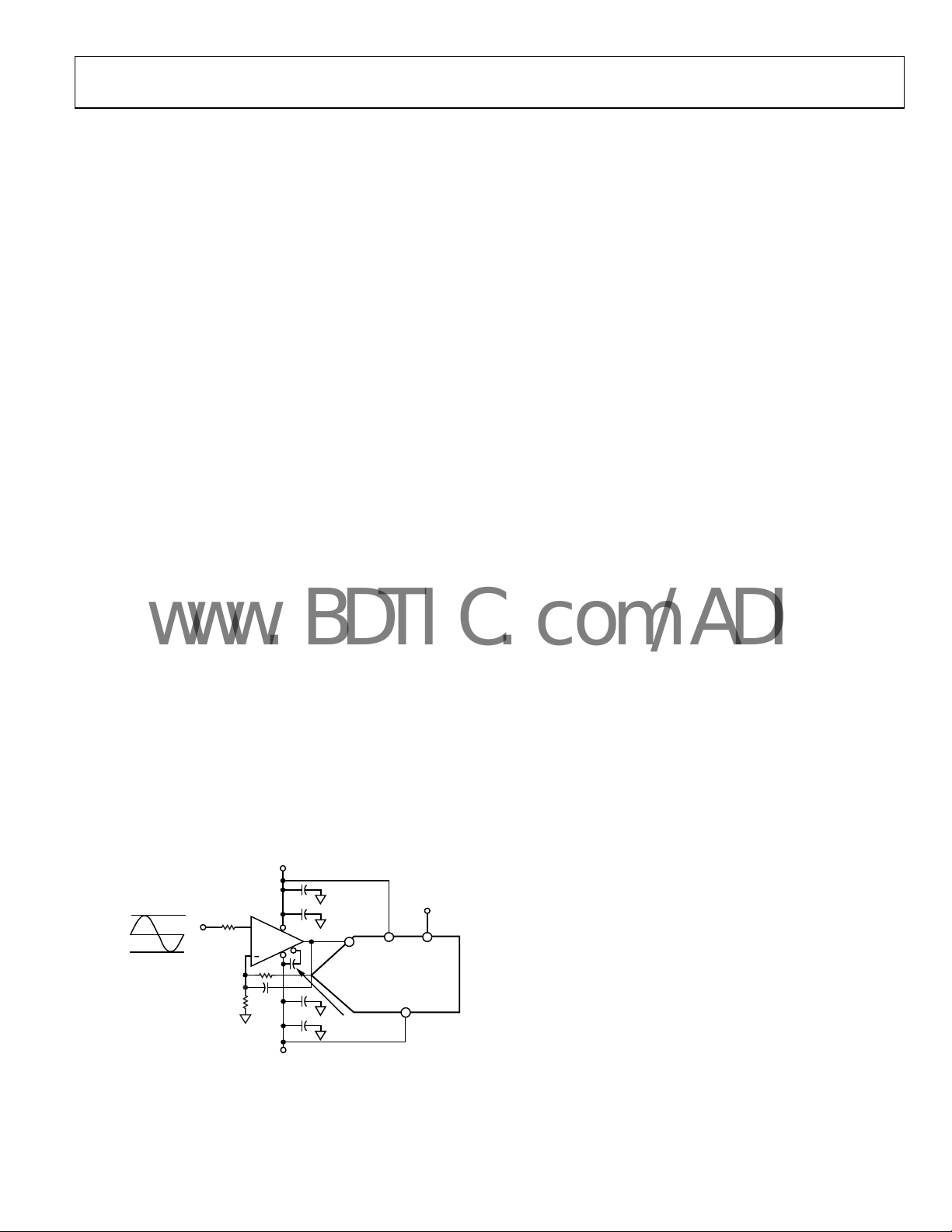
DRIVER AMPLIFIER CHOICE
Each AD7366-5/AD7367-5 has a total of four analog inputs,
which operate in single-ended mode. Both ADC analog inputs
can be programmed to one of the three analog input ranges. In
applications where the signal source is high impedance, it is
recommended to buffer the signal before applying it to the
ADC analog inputs.
AD7366-5
/AD7367-5 in single-ended mode.
In applications where the THD and SNR are critical specifi-
tions, the analog input of the AD7366-5/AD7367-5 should be
ca
driven from a low impedance source. Large source impedances
significantly affect the ac performance of the ADC and can
necessitate the use of an input buffer amplifier.
When no amplifier is used to drive the analog input, the source
mpedance should be limited to low values. The maximum source
i
impedance depends on the amount of THD that can be tolerated
in the application. The THD increases as the source impedance
increases and performance degrades.
th
e analog input frequency for various source impedances.
Depending on the input range and analog input configuration
selected, the AD7366-5/AD7367-5 can handle source
impedances as illustrated in
Due to the programmable nature of the analog inputs on the
AD7366-5
/AD7367-5, the choice of op amp used to drive the
inputs is a function of the particular application and depends
on the selected analog input voltage ranges.
The driver amplifier must be able to settle for a full-scale step to
a 1
4-bit level, 0.0061%, in less than the specified acquisition time
of the AD7366-5/AD7367-5. An op amp such as the AD8021
m
eets this requirement when operating in single-ended mode.
The AD8021 needs an external compensating NPO type of
ca
pacitor. The AD8022 can also be used in high frequency
a
pplications where a dual version is required. For lower frequency
applications, recommended op amps are the
nd AD8610.
a
+10V/+5V
AGND
–10V/–5V
Figure 21. Typical Connection Diagram with the AD8021
Driv
Figure 21 shows the configuration of the
Figure 7 shows THD vs.
Figure 7.
AD797, AD845,
+
+
10µF
+
0.1µF
+
AD8021
1k
15pF
1k
*ADDITIO NAL PINS OMITT ED FOR CLARI TY.
ing the Analog Input in Single-Ended Mode
0.1µF
10µF
V–
V
A1
AD7366-5/
C
COMP
AD7367-5*
= 10pF
+
+
V
DD
DVCC/AV
V
SS
+5V
CC
06842-023
DRIVE
The AD7366-5/AD7367-5 also have a V
the voltage at which the serial interface operates. V
feature to control
DRIVE
DRIVE
allows
the ADC to easily interface to both 3 V and 5 V processors. For
example, if the AD7366-5/AD7367-5 is operated with a V
5 V, the V
pin could be powered from a 3 V supply, allowing
DRIVE
of
CC
a large dynamic range with low voltage digital processors. Thus,
the AD7366-5/AD7367-5 could be used with the ±10 V input
range while still being able to interface to 3 V digital parts.
REFERENCE
The AD7366-5/AD7367-5 can operate with either the internal
2.5 V on-chip reference or an externally applied reference. The
logic state of the REFSEL pin determines whether the internal
reference is used. The internal reference is selected for both ADCs
when the REFSEL pin is tied to logic high. If the REFSEL pin is
tied to GND, an external reference can be supplied through the
D
A and D
CAP
tied to either a low logic or high logic state for the part to operate.
Suitable reference sources for the AD7366-5/AD7367-5 include
the
AD780, AD1582, ADR431, REF193, and ADR391.
The internal reference circuitry consists of a 2.5 V band gap
eference and a reference buffer. When operating the AD7366-5/
r
AD7367-5 in internal reference mode, the 2.5 V internal reference
is available at the D
decoupled to AGND using a 680 nF capacitor. It is recommended
that the internal reference be buffered before applying it elsewhere
in the system. The internal reference is capable of sourcing up
to 150 A with an analog input range of ±10 V and 70 µA for
both the ±5 V range and 0 V to +10 V range
If the internal reference operation is required for the ADC
version, the REFSEL pin must be tied to logic high on power-
con
up. The reference buffer requires 70 µs to power up and charge
the 680 nF decoupling capacitor during the power-up time.
The AD7366-5/AD7367-5 is specified for a 2.5 V to 3 V reference
r
ange. When a 3 V reference is selected, the ranges are ±12 V,
±6 V, and 0 V to +12 V. For these ranges, the V
must be greater than or equal to the +12 V and −12 V, respectively.
B pins. On power-up, the REFSEL pin must be
CAP
A and D
CAP
B pins, which should be
CAP
and VSS supply
DD
Rev. 0 | Page 19 of 28
AD7366-5/AD7367-5
www.BDTIC.com/ADI
MODES OF OPERATION
The mode of operation for the AD7366-5/AD7367-5 is selected
CNVST
by the (logic) state of the
signal at the end of a conversion. There are two possible modes of operation: normal mode
and shutdown mode. These modes of operation are designed to
provide flexible power management options, which can be
chosen to optimize the power dissipation/throughput rate
ratio for differing application requirements.
NORMAL MODE
Normal mode is intended for applications needing fast
throughput rates because the user does not have to worry
about any power-up times (with the AD7366-5/AD7367-5
remaining fully powered at all times). Figure 22 shows the
n
ormal mode of operation for the AD7366-5, while Figure 23
il
lustrates normal mode for the AD7367-5.
The conversion is initiated on the falling edge of
described in the Circuit Information section. To ensure that
e part remains fully powered up at all times,
th
at a logic high state prior to the BUSY signal going low. If
CNVST
is at a logic low state when the BUSY signal goes low,
the analog circuitry powers down and the part ceases converting.
CNVST
CNVST
as
must be
The BUSY signal remains high for the duration of the conversion.
CS
pin must be brought low to bring the data bus out of
The
three-state; subsequently 12 SCLK cycles are required to read
the conversion result from the AD7366-5, while 14 SCLK cycles
are required to read from the AD7367-5. The D
to three-state only when
CS
is brought high. If CS is left low for
lines return
OUT
a further 12 SCLK cycles for the AD7366-5 or 14 SCLK cycles
for the AD7367-5, the result from the other on-chip ADC is
also accessed on the same D
line, as shown in Figure 27 and
OUT
Figure 28 (see the Serial Interface section).
After 24 SCLK cycles have elapsed for the AD7366-5 and 28 SCLK
c
ycles have elapsed for the AD7367-5, the D
three-state when
falling edge). If
CS
is brought high (not on the 24th or 28th SCLK
CS
is brought high prior to this, the D
returns to three-state at that point. Thus,
line returns to
OUT
CS
must be brought
OUT
line
high once the read is completed because the bus does not
automatically return to three-state upon completion of the
dual result read.
Once a data transfer is complete and D
A and D
OUT
OUT
B have
returned to three-state, another conversion can be initiated after
the quiet time, t
, has elapsed by bringing
QUIET
CNVST
low again.
t
1
CNVST
t
QUIET
12
06842-024
BUSY
CS
SCLK
t
2
t
CONVERT
SERIAL READ OPERATION
Figure 22. Normal Mode Operation for the AD7366-5
t
3
1
t
1
CNVST
t
QUIET
BUSY
CS
t
2
t
CONVERT
t
3
SCLK
SERIAL READ OPERATION
1
Figure 23. Normal Mode Operation for the AD7367-5
Rev. 0 | Page 20 of 28
14
06842-025

AD7366-5/AD7367-5
www.BDTIC.com/ADI
SHUTDOWN MODE
Shutdown mode is intended for use in applications where slow
throughput rates are required. Shutdown mode is suited to
applications where a series of conversions performed at a
relatively high throughput rate are followed by a long period of
inactivity and, thus, shutdown. When the AD7366-5/AD7367-5
are in full power-down, all analog circuitry is powered down.
CNVST
The falling edge of
output subsequently goes high to indicate that the conversion is
in progress. Once the conversion is completed, the BUSY output
returns low. If the
CNVST
goes low, the part enters shutdown at the end of the conversion
phase. While the part is in shutdown mode, the digital output
code from the last conversion on each ADC can still be read
from the D
pins. To read the D
OUT
low as described in the Serial Interface section. The D
return to three-state once
To exit full power-down and to power up the AD7366-5/
AD7367-5,
a rising edge of
required power-up time has elapsed,
low again to initiate another conversion, as shown in Figure 24
initiates the conversion. The BUSY
signal is at logic low when BUSY
data, CS must be brought
OUT
pins
OUT
CS
is brought back to logic high.
CNVST
is required. After the
CNVST
may be brought
POWER-UP TIMES
As described in the Shutdown Mode section, the AD7366-5/
AD7367-5 have one power-down mode. This section deals with
the power-up time required when coming out of this mode. It
should be noted that these power-up times apply with the
recommended capacitors in place on the D
To p o wer up f rom s hut d ow n ,
CNVST
must be brought high and
remain high for a minimum of 70 s, as shown in Figure 24.
When power supplies are first applied to the AD7366-5/AD7367-5,
CNVST
th
e ADC can power up with
in either the low or high
logic state. Before attempting a valid conversion,
be brought high and remain high for the recommended powerup time of 70 s.
CNVST
can then be brought low to initiate a
conversion. With the AD7366-5/AD7367-5, no dummy conversion
is required before valid data can be read from the
If it is intended to place the part in shutdown mode when the
upplies are first applied, the AD7366-5/AD7367-5 must be
s
powered up, and a conversion initiated. However,
should remain in the logic low state, and when the BUSY signal
goes low, the part enters shutdown.
Once supplies are applied to the AD7366-5/AD7367-5, sufficient
ime must be allowed for any external reference to power up
t
and to charge the various reference buffer decoupling capacitors
to their final values.
A and D
CAP
CAP
CNVST
D
OUT
CNVST
B pins.
must
pins.
t
POWER- UP
06842-026
CNVST
BUSY
CS
SCLK
ENTERS SHUTDOWN
t
2
t
CONVERT
t
3
1
Figure 24. Autoshutdown M
ode for AD7366-5
SERIAL READ OPERATION
12
Rev. 0 | Page 21 of 28

AD7366-5/AD7367-5
www.BDTIC.com/ADI
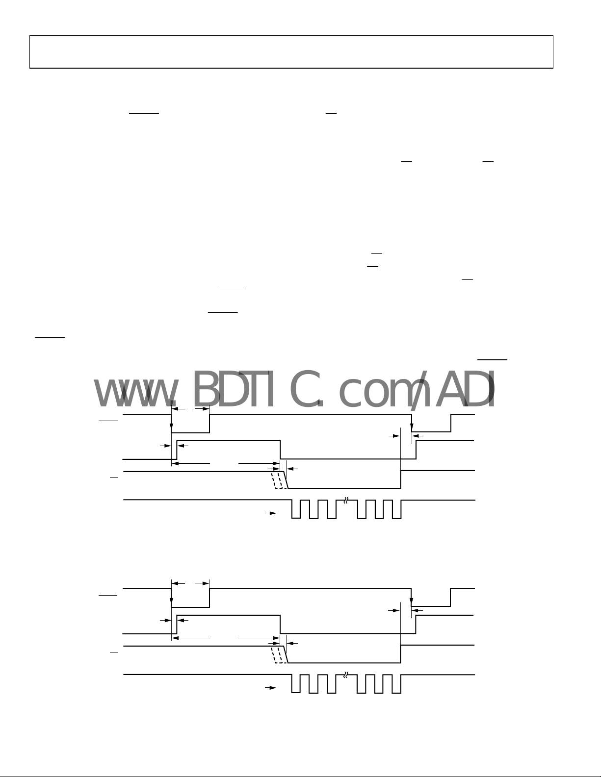
SERIAL INTERFACE
Figure 25 and Figure 26 show the detailed timing diagrams for
serial interfacing to the AD7366-5 and the AD7367-5, respectively.
On the falling edge of
CNVST
, the AD7366-5/AD7367-5 simultaneously converts the selected channels. These conversions are
performed using the on-chip oscillator. After the falling edge of
CNVST
, the BUSY signal goes high, indicating the conversion has
started. It returns low once the conversion has been completed.
D
The data can now be read from the
OUT
pins.
On the rising edge of
and D
B go back into three-state. If CS is not brought high,
OUT
but is instead held low for a further 12 SCLK cycles for the
AD7366-5 or 14 SCLK cycles for the AD7367-5 on either D
B, the data from the other ADC follows on that D
or D
OUT
This is illustrated in
D
A is shown. In this case, the D
OUT
three-state on the rising edge of
CS
, the conversion is terminated, and D
OUT
OUT
OUT
pin.
Figure 27 and Figure 28 where the case for
line in use goes back into
OUT
CS
.
A
A
CS
and SCLK signals are required to transfer data from the
AD7366-5/AD7367-5. The parts have two output pins corresponding to each ADC. Data can be read from the AD7366-5/
AD7367-5 using both D
A and D
OUT
B. Alternatively, a single
OUT
output pin of the user’s choice can be used. The SCLK input signal
provides the clock source for the serial interface. The
CS
goes
low to access data from the AD7366-5/AD7367-5. The falling edge
CS
of
takes the bus out of three-state and clocks out the MSB of
the conversion result. The data stream consists of 12 bits of data
for the AD7366-5 and 14 bits of data for the AD7367-5, MSB first.
The first bit of the conversion result is valid on the first SCLK
falling edge after the
CS
falling edge. The subsequent 11-bits/
13-bits of data for the AD7366-5/AD7367-5, respectively, are
clocked out on the falling edge of the SCLK signal. A minimum
of 12 clock pulses must be provided to the AD7366-5 to access
each conversion result, while a minimum of 14 clock pulses must
be provided to the AD7367-5 to access the conversion result.
Figure 25 shows how a 12 SCLK read is used to access the
nversion results, while Figure 26 illustrates the case for the
co
AD7367-5
with a 14 SCLK read.
CS
If the falling edge of SCLK coincides with the falling edge of
CS
the falling edge of SCLK is not acknowledged by the AD7366-5/
AD7367-5, and the next falling edge of the SCLK is the first
registered after the falling edges of the
CS
pin can be brought low before the BUSY signal goes low,
The
indicating the end of a conversion. Once
CS
.
CS
is at a logic low state,
the data bus is brought out of three-state. This feature can be
utilized to ensure that the MSB is valid on the falling edge of
BUSY by bringing
signal goes low. The dotted
CS
low a minimum of t4 ns before the BUSY
CS
line in Figure 22 and Figure 23
illustrates this.
CS
Alternatively, the
ously. In this case, the D
pin can be tied to a low logic state continu-
pins never enter three-state, and the
OUT
data bus is continuously active. Under these conditions, the MSB
of the conversion result for the AD7366-5/AD7367-5 is available
on the falling edge of the BUSY signal. The next most significant
bit is available on the first SCLK falling edge after the BUSY
signal has gone low. This mode of operation enables the user to
read the MSB as soon as it is made available by the converter.
,
t
8
SCLK
D
OUT
D
OUT
A
B
THREESTATE
DB11
1
t
2
4
DB10
34
DB9 DB8 DB2 DB1 DB0
Figure 25. Serial Interface Timing Diagram for the AD7366-5
512
t
t
t
5
6
7
t
9
CS
t
8
SCLK
D
D
OUT
OUT
A
B
THREESTATE
DB13
1
t
2
4
DB12
34
DB11 DB10 DB2 DB1 DB0
Figure 26. Serial Interface Timing Diagram for the AD7367-5
514
t
t
t
5
6
7
t
9
Rev. 0 | Page 22 of 28
THREE-STATE
THREE-STATE
06842-027
6842-028

AD7366-5/AD7367-5
www.BDTIC.com/ADI
CS
t
SCLK
D
OUT
A
THREESTATE
DB11
2
DB9
A
34
1
t
4
DB10
A
A
Figure 27. Reading Data from Both ADCs on One D
8
5
10
DB1
11
t
6
DB0
A
A
t
7
t
5
13 24
12
DB10
DB11
Line with 24 SCLKs for the AD7366-5
OUT
B
B
DB1
DB0
B
B
THREESTATE
06842-030
CS
t
SCLK
D
OUT
A
THREESTATE
DB13
2
DB11
34
A
1
t
3
DB12
A
A
Figure 28. Reading Data from Both ADCs on One D
8
5
12
DB1
13
t
6
DB0
A
A
t
7
t
5
15 28
14
DB12
DB13
Line with 28 SCLKs for the AD7367-5
OUT
B
B
DB1
DB0
B
B
THREESTATE
06842-029
Rev. 0 | Page 23 of 28

AD7366-5/AD7367-5
www.BDTIC.com/ADI
MICROPROCESSOR INTERFACING
The serial interface on the AD7366-5/AD7367-5 allows the
parts to be directly connected to a range of different microprocessors. This section explains how to interface the AD7366-5/
AD7367-5 with some more common microcontrollers and DSP
serial interface protocols.
AD7366-5/AD7367-5 TO ADSP-218x
The ADSP-218x family of DSPs interfaces directly to the
AD7366-5/AD7367-5 with no glue logic required. The V
pin of the AD7366-5/AD7367-5 takes the same supply voltage
as that of the ADSP-218x. This allows the ADC to operate at a
higher supply voltage than its serial interface and therefore, the
ADSP-218x, if necessary. The connection diagram in
sho
ws both D
A and D
OUT
B of the AD7366-5/AD7367-5
OUT
connected to both serial ports of the ADSP-218x. The SPORT0
and SPORT1 control registers should be set up as shown in
Tabl e 1 1 and Tabl e 12.
AD7366-5/
AD7367-5*
SCLK
CS
D
A
OUT
D
B DR1
OUT
CNVST FLn
V
DRIVE
ADSP-218x*
SCLK0
SCLK1
TFS0
RFS0
RFS1
DR0
IRQnBUSY
DRIVE
Figure 29
Table 11. SPORT0 Control Register Setup
Setting Description
TFSW = RFSW = 1 Alternate framing.
INVRFS = INVTFS = 1 Active low frame signal.
DTYPE = 00 Right justify data.
SLEN = 1111
16-bit data-word (or can be set to 1101
or 14-bit data-word).
f
ISCLK = 1 Internal serial clock.
TFSR = RFSR = 1 Frame every word.
IRFS = 0
ITFS = 1
Table 12. SPORT1 Control Register Setup
Setting Description
TFSW = RFSW = 1 Alternate framing.
INVRFS = INVTFS = 1 Active low frame signal.
DTYPE = 00 Right justify data.
SLEN = 1111
16-bit data-word (or can be set to 1101
or 14-bit data-word).
f
ISCLK = 0 External serial clock.
TFSR = RFSR = 1 Frame every word.
IRFS = 0
ITFS = 1
The ADSP-218x has the TFS0 and RFS0 of the SPORT0 and the
RFS1 of SPORT1 tied together. TFS0 is set as an output, and both
RFS0 and RFS1 are set as inputs. The DSP operates in alternate
framing mode, and the SPORT control registers are set up as
described in Table 11 and Table 12. The frame synchronization
signal generated on the TFS0 is tied to
CS
.
V
DD
*ADDITIONAL PINS OMITTED FOR CLARITY.
Figure 29. Interfacing the AD7366-5/AD7367-5 to the ADSP-218x
The AD7366-5/AD7367-5 BUSY line provides an interrupt to
he ADSP-218x when the conversion is complete. The conversion
06842-031
t
results can then be read from the AD7366-5/AD7367-5 using a
read operation. When an interrupt is received on
BUSY signal, a value is transmitted with TFS/DT (ADC control
word). The TFS is used to control the RFS and, therefore, the
reading of data.
Rev. 0 | Page 24 of 28
IRQn
from the

AD7366-5/AD7367-5
www.BDTIC.com/ADI
AD7366-5/AD7367-5 TO ADSP-BF53x
The ADSP-BF53x family of DSPs interfaces directly to the
AD7366-5/AD7367-5 with no glue logic required. The availability
of secondary receive registers on the serial ports of the Blackfin®
DSPs means that only one serial port is necessary to read from
both D
D
OUT
Serial Port 0 of the ADSP-BF53x. The SPORT0 Receive
Configuration 1 register and SPORT0 Receive Configuration 2
register should be set up as outlined in
Table 13. SPORT0 Receive Configuration 1 Register
(SPORT0_RCR1) Setup
Setting Description
RCKFE = 1 Sample data with falling edge of RSCLK.
LRFS = 1 Active low frame signal.
RFSR = 1 Frame every word.
IRFS = 1 Internal RFS used.
RLSBIT = 0 Receive MSB first.
RDTYPE = 00 Zero fill.
IRCLK = 1 Internal receive clock.
RSPEN = 1 Receive enabled.
SLEN = 1111
TFSR = RFSR = 1
Table 14. SPORT0 Receive Configuration 2 Register
(SPORT0_RCR2) Setup
Setting Description
RXSE = 1 Secondary side enabled.
SLEN = 1111
A and D
OUT
A and D
OUT
B pins simultaneously. Figure 30 shows
OUT
B of the AD7366-5/AD7367-5 connected to
Tabl e 1 3 and Tabl e 1 4 .
AD7366-5/
AD7367-5*
D
A
OUT
SCLK
CS
CNVST
B
OUT
V
DRIVE
*ADDITIONAL PINS OMITTED FOR CLARITY.
Figure 30. Interfacing the AD7366-5/AD7367-5 to the ADSP-BF53x
SERIAL
DEVICE A
(PRIMARY)
SERIAL
DEVICE B
(SECONDARY)
ADSP-BF53x*
SPORT0
DR0PRI
RCLKO
RFS0
RXINPUTSBUSY
PFn
DR0SECD
V
DD
16-bit data-word (or can be set to 1101 for
14-bit da
ta-word).
16-bit data-word (or can be set to 1101 for
14-bit da
ta-word).
6842-032
AD7366-5/AD7367-5 TO TMS320VC5506
The serial interface on the TMS320VC5506 uses a continuous
serial clock and frame synchronization signals to synchronize
the data transfer operations with peripheral devices like the
AD7366-5/AD7367-5. The
between the TMS320VC5506 and the AD7366-5/AD7367-5
with no glue logic required. The serial ports of the TMS320VC5506
are set up to operate in burst mode with internal CLKX0 (Tx
serial clock on Serial Port 0) and FSX0 (Tx frame sync from
Serial Port 0). The connection diagram is shown in
T
he serial port control registers (SPC) must be setup as shown
in
Tabl e 1 5 .
AD7366-5/
AD7367-5*
*ADDITIONAL PINS OMITTED FOR CLARITY.
Figure 31. Interfacing the AD7366-5/AD7367-5 to the TMS320VC5506
SCLK
D
A
OUT
B
D
OUT
CS FSX0
BUSY
CNVST
V
DRIVE
Table 15. Serial Port Control Register Setup
SPC FO FSM MCM TXM
SPC0 0 1 1 1
SPC1 0 1 0 0
The V
pin of the AD7366-5/AD7367-5 takes the same
DRIVE
supply voltage as that of the TMS320VC5506. This allows the
ADC to operate at a higher voltage than its serial interface and,
therefore, the TMS320VC5506, if necessary.
As with the previous interfaces, conversion can be initiated
from the
TMS320VC5506 or from an external source, and the
processor is interrupted when the conversion sequence is
complete.
CS
input allows easy interfacing
Figure 31.
TMS320VC5506*
CLKX0
CLKR0
CLKX1
CLKR1
DR0
DR1
FSR0
FSR1
INTn
XF
V
DD
06842-033
Rev. 0 | Page 25 of 28

AD7366-5/AD7367-5
www.BDTIC.com/ADI
AD7366-5/AD7367-5 TO DSP563xx
The connection diagram in Figure 32 shows how the AD7366-5/
AD7367-5 can be connected to the enhanced synchronous
serial interface (ESSI) of the DSP563xx family of DSPs from
Motorola. There are two on-board ESSIs, and each is operated in
synchronous mode (Bit SYN = 1 in the CRB register) with
internally generated word length frame sync for both Tx and Rx
(Bit FSL1 = 0 and Bit FSL0 = 0 in the CRB register).
AD7366-5/
AD7367-5*
D
D
CNVST
V
SCLK
OUT
OUT
CS
BUSY
DRIVE
A
B
DSP563xx*
SCK0
SCK1
SRD0
SRD1
SC02
SC12
IRQn
PBn
Normal operation of the ESSI is selected by making MOD = 0 in
the CRB register. Set the word length to 16 by setting Bit WL1 = 1
and Bit WL0 = 0 in the CRA register. The FSP bit in the CRB
register should be set to 1 so that the frame sync is negative.
In Figure 32, the serial clock is taken from the ESSI0 so the SCK0
p
in must be set as an output (SCKD = 1) while the SCK1 pin is set
as an input (SCKD = 0). The frame sync signal is taken from SC02
on ESSI0, so SCD2 = 1, while on ESSI1, SCD2 = 0; therefore, SC12
is configured as an input. The V
pin of the AD7366-5/
DRIVE
AD7367-5 takes the same supply voltage as that of the DSP563xx.
This allows the ADC to operate at a higher voltage than its
serial interface and, therefore, the DSP563xx, if necessary.
*ADDITIONA L PINS OMITTED FOR CLARITY.
Figure 32. Interfacing the AD7366-5/AD7367-5 to the DSP563xx
V
DD
06842-034
Rev. 0 | Page 26 of 28

AD7366-5/AD7367-5
www.BDTIC.com/ADI
APPLICATION HINTS
LAYOUT AND GROUNDING
The printed circuit board that houses the AD7366-5/AD7367-5
should be designed so that the analog and digital sections are
confined to their own separate areas of the board. This design
facilitates the use of ground planes that can be easily separated.
To provide optimum shielding for ground planes, a minimum
et
ch technique is generally the best option. All AGND pins on
the AD7366-5/AD7367-5 should be connected to the AGND
plane. Digital and analog ground pins should be joined in only
one place. If the AD7366-5/AD7367-5 are in a system where
multiple devices require an AGND and DGND connection, the
connection should still be made at only one point. A star point
should be established as close as possible to the ground pins on
the AD7366-5/AD7367-5.
Good connections should be made to the power and ground
lanes. This can be done with a single via or multiple vias for
p
each supply and ground pin.
Avoid running digital lines under the AD7366-5/AD7367-5
vices because this couples noise onto the die. However, the
de
analog ground plane should be allowed to run under the
AD7366-5/AD7367-5 to avoid noise coupling. The power
supply lines to the AD7366-5/AD7367-5 should use as large
a trace as possible to provide low impedance paths and reduce
the effects of glitches on the power supply line.
To avoid radiating noise to other sections of the board, comp
onents such as clocks with fast switching signals, should be
shielded with digital ground and should never be run near the
analog inputs. Avoid crossover of digital and analog signals. To
reduce the effects of feedthrough within the board, traces should
be run at right angles to each other. A microstrip technique is
the best method, but its use may not be possible with a doublesided board. In this technique, the component side of the board
is dedicated to ground planes, and signals are placed on the
other side.
Good decoupling is also important. All analog supplies should
be
decoupled with 10 µF tantalum capacitors in parallel with
0.1 µF capacitors to AGND. To achieve the best results from
these decoupling components, they must be placed as close as
possible to the device, ideally right up against the device. The
0.1 µF capacitors should have a low effective series resistance
(ESR) and low effective series inductance (ESI), such as is typical
of common ceramic and surface mount types of capacitors. These
low ESR, low ESI capacitors provide a low impedance path to
ground at high frequencies to handle transient currents due to
internal logic switching.
EVALUATING THE AD7366-5/AD7367-5
Evaluation boards for the AD7366 and AD7367, the
EVAL-AD7366CBZ and EVAL-AD7367CBZ, can also be
used to evaluate the performance of the AD7366-5 and
AD7367-5, respectively. These evaluation boards can be
used in conjunction with EVAL-CONTROL BRD2 to
provide a full-featured evaluation platform.
Rev. 0 | Page 27 of 28

AD7366-5/AD7367-5
www.BDTIC.com/ADI
OUTLINE DIMENSIONS
7.90
7.80
7.70
24
PIN 1
0.15
0.05
0.10 COPLANARITY
Figure 33. 24-Lead Thin Shrink S
0.65
BSC
0.30
0.19
COMPLIANT TO JEDEC STANDARDS MO-153-AD
Dimensions shown in millimeters
13
4.50
4.40
4.30
121
1.20
MAX
SEATING
PLANE
(RU-24)
6.40 BSC
0.20
0.09
mall Outline Package [TSSOP]
8°
0°
0.75
0.60
0.45
ORDERING GUIDE
Model Temperature Range Package Description Package Option
AD7366BRUZ-5
AD7366BRUZ-5-RL7
AD7366BRUZ-5500RL7
AD7367BRUZ-5
AD7367BRUZ-5-RL7
AD7367BRUZ-5500RL7
1
Z = RoHS Compliant Part.
1
1
1
1
−40°C to +85°C 24-Lead Thin Shrink Small Outline Package [TSSOP] RU-24
−40°C to +85°C 24-Lead Thin Shrink Small Outline Package [TSSOP] RU-24
1
−40°C to +85°C 24-Lead Thin Shrink Small Outline Package [TSSOP] RU-24
−40°C to +85°C 24-Lead Thin Shrink Small Outline Package [TSSOP] RU-24
−40°C to +85°C 24-Lead Thin Shrink Small Outline Package [TSSOP] RU-24
1
−40°C to +85°C 24-Lead Thin Shrink Small Outline Package [TSSOP] RU-24
©2007 Analog Devices, Inc. All rights reserved. Trademarks and
registered trademarks are the property of their respective owners.
D06842-0-7/07(0)
Rev. 0 | Page 28 of 28
 Loading...