True Bipolar Input, Dual
www.BDTIC.com/ADI
Preliminary Technical Data
FEATURES
Dual 14-bit, 2-channel ADC
True Bipolar Analog Inputs
Programmable Input Ranges
±10, ±5, 0 to 10 V
Throughput rate: 1 MSPS
Simultaneous conversion with read in 1μs
Specified for V
Low current consumption: 5.65 mA max
Wide input bandwidth
14 bits No Missing Codes
On-chip reference: 2.5 V
–40°C to +85°C operation
High speed serial interface
SPI®/QSPI™/MICROWIRE™/DSP compatible
TM
iCMOS
24-lead TSSOP package
For 12 bit version see AD7366
GENERAL DESCRIPTION
of 5 V±5%
CC
Process Technology
1μs, 14-Bit, 2-Channel SAR ADC
AD7367
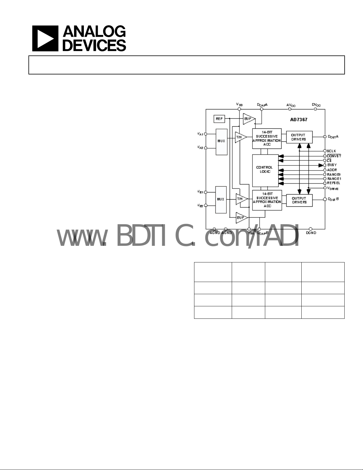
FUNCTIONAL BLOCK DIAGRAM
The AD73671 is a dual, 14-bit, high speed, low power, successive
approximation ADC that features throughput rates up to 1
MSPS. The device contains two ADCs, each preceded by a 2channel multiplexer, and a low noise, wide bandwidth trackand-hold amplifier that can handle input frequencies in excess
of 10 MHz.
The AD7367 is fabricated on Analog Devices’ Industrial CMOS
process, iCMOS, a technology platform combining the
advantages of low and high voltage CMOS, bipolar and high
voltage DMOS processes. The process allows the AD7367 to
accept high voltage bipolar signals in addition to reducing
power consumption and package size.
The AD7367 can accept true bipolar analog input signals in the
±10 V range, ±5 V range and 0 to 10 V range.
The AD7367 has an on-chip 2.5 V reference that can be
overdriven if an external reference is preferred. The AD7367 is
available in a 24-lead TSSOP package.
1
Protected by U.S. Patent No. 6,681,332.
TM
iCMOS
Process Technology
For analog systems designers within industrial/instrumentation equipment OEMs who need high performance ICs at higher-voltage levels, iCMOS is a technology
platform that enables the development of analog ICs capable of 30V and operating at +/- 15V supplies while allowing dramatic reductions in power consumption and
package size, and increased AC and DC performance.
Table 1.Related Products
Device
Number
AD7366 12-Bit 1 MSPS Dual, 2-ch
AD7366-5 12-Bit 500 KSPS Dual, 2-ch
AD7367-5 14-Bit 500 KSPS Dual, 2-ch
Resolution Throughput
Figure 1
Rate
Number of
Channels
Rev. PrD
Information furnished by Analog Devices is believed to be accurate and reliable. However, no
responsibility is assumed by Anal og Devices for its use, nor for any infringements of patents or ot her
rights of third parties that may result from its use. Specifications subject to change without notice. No
license is granted by implication or otherwise under any patent or patent rights of Analog Devices.
Trademarks and registered trademarks are the property of their respective owners.
One Technology Way, P.O. Box 9106, Norwood, MA 02062-9106, U.S.A.
Tel: 781.329.4700 www.analog.com
Fax: 781.461.3113 ©2006 Analog Devices, Inc. All rights reserved.

AD7367 Preliminary Technical Data
www.BDTIC.com/ADI
TABLE OF CONTENTS
FEATURES........................................................................................ 1
Analog Inputs ............................................................................. 11
GENERAL DESCRIPTION ............................................................ 1
FUNCTIONAL BLOCK DIAGRAM............................................. 1
Revision History ............................................................................... 2
Specifications..................................................................................... 3
Timing Specifications .................................................................. 5
Absolute Maximum Ratings............................................................ 6
ESD Caution.................................................................................. 6
Pin Configuration and Function Descriptions............................. 7
Terminology ...................................................................................... 9
Theory of operation ...................................................................10
REVISION HISTORY
4/06—PRA: Initial Version
5/06—PRA changes to PRB: Initial Version
10/06—PRB changes to PRC: Modified Supply specifications
V
............................................................................................ 12
DRIVE
Reference ..................................................................................... 12
Modes of Operation ....................................................................... 12
NORMAL MODE ...................................................................... 12
Shut-down Mode........................................................................ 12
POWER-UP TIMES................................................................... 12
Serial Interface ................................................................................ 12
Outline Dimensions....................................................................... 12
Ordering Guide............................................................................... 12
Rev. PrD | Page 2 of 16

AD7367 Preliminary Technical Data
www.BDTIC.com/ADI
SPECIFICATIONS
AVCC = DVCC =4.75 V to 5.25 V, VDD = 11.5 V to 16.5 V, VSS = −11.5 V to −16.5 V, V
V
= 2.5 V Internal/External; TA = T
REF
MIN
to T
, unless otherwise noted1.
MAX
Table 2.
Parameter Min Typ Max Unit Test Conditions/
DYNAMIC PERFORMANCE fIN = 50 kHz sine wave;
Signal-to-Noise Ratio (SNR)
Signal-to-Noise + Distortion Ratio
2
(SINAD)
Total Harmonic Distortion (THD)
Spurious Free Dynamic Range (SFDR)
Intermodulation Distortion (IMD)
2
TDB 79 dB
TBD 78 dB
2
2
2
-85 TBD dB
-85 TBD dB
fa = 49 kHz, fb = 51 kHz
Second Order Terms -91 dB
Third Order Terms
Channel-to-Channel Isolation
2
-89 dB
-88 dB
SAMPLE AND HOLD
Aperture Delay3 10 ns
Aperture Jitter3 40 ps
Aperture Delay Matching3 100 ps
Full Power Bandwidth 65 MHz @ 3 dB, ±10 V range
15 MHz @ 0.1 dB, ±10 V range
DC ACCURACY
Resolution 14 Bits
Integral Nonlinearity
Differential Nonlinearity
2
2
±2 LSB
±0.99 LSB Guaranteed no missed codes to 14 bits
Positive Full Scale Error2 ±5 LSB
Positive Full Scale Error Match2 ±0.5 LSB
Zero Code Error2 ±1 LSB
Zero Code Error Match2 ±1 LSB
Negative Full Scale Error2 ±5 LSB
Negative Full Scale Error Match2 ±0.5 LSB
ANALOG INPUT
Input Voltage Ranges ±10 V
(Programmed via RANGE Pins) ±5 V
0 to
10V
See Table 6.
DC Leakage Current ±1 µA
Input Capacitance 12 p When in track, ±10 V range
15 pF When in track, ±5 V or 0 to 10 V range
3 pF When in hold
Input impedance 260 KΩ For ±10V @1 Msps
2.3 MΩ For ±10V @100 Ksps
125 KΩ For ±5 / 0-10V @1 Msps
1.1 MΩ For ±5 / 0-10V @100Ksps
= 2.7 V to 5.25V, f
DRIVE
V
SAMPLE
= 1MSPS, f
= 48MHz,
SCLK
Comments
= +11.5V min, VSS = −11.5V min, VCC
V
DD
= 4.75V to 5.25V
= +11.5V min, VSS = −11.5V min, VCC
V
DD
= 4.75V to 5.25V
= +11.5V min, VSS = -11.5V min, VCC
V
DD
= 4.75V to 5.25V
Rev. PrD | Page 3 of 16

AD7367 Preliminary Technical Data
www.BDTIC.com/ADI
Parameter Min Typ Max Unit Test Conditions/
Comments
REFERENCE INPUT/OUTPUT
Reference Output Voltage
Reference Input Voltage Range +2.5 3.0 V
DC Leakage Current ±1 µA
Input Capacitance 25 pF
V
A, V
REF
B Output Impedance
REF
Reference Temperature Coefficient 10 20 ppm/°C
V
Noise 20 µV
REF
LOGIC INPUTS
Input High Voltage, V
Input Low Voltage, V
Input Current, IIN ±1 µA max VIN = 0 V or V
Input Capacitance, C
LOGIC OUTPUTS
Output High Voltage, VOH V
Output Low Voltage, VOL 0.4 V
Floating State Leakage Current ±1 µA
Floating State Output Capacitance
CONVERSION RATE
Conversion Time 680 ns
Track/Hold Acquisition Time
Throughput Rate 1 MSPS For 4.75V≤V
900 KSPS For 2.7V≤V
POWER REQUIREMENTS Digital I/Ps = 0 V or V
V
CC
V
DD
V
SS
V
2.7 5.25 V
DRIVE
Normal Mode (Static)
IDD 250 µA VDD = +16.5 V
ISS 50 µA VSS = −16.5 V
ICC 1.8 mA VCC = 5.5 V
Normal Mode (Operational) fs = 1 MSPS
IDD 925 µA VDD = +16.5 V
ISS 725 µA VSS = −16.5 V
ICC 4 mA VCC = 5.25 V, internal reference enabled
Shut-Down Mode
IDD 1 µA VDD = +16.5 V
ISS 1 µA VSS = −16.5 V
ICC 1 µA VCC = 5.25 V
Power Dissipation
Normal Mode (Operational) 48.23 mW VDD = +16.5V, VSS = −16.5V, VCC = 5.25V
Shut-Down 15 µW VDD = +5V, VSS = −5V, VCC = 5V
Shut-Down 38.25 µW VDD = +16.5V, VSS = −16.5V, VCC = 5.25
1
Temperature range is −40°C to +85°C
2
See Terminology section.
3
Sample tested during initial release to ensure compliance.
4
Refers to pins V
REF
A or V
REF
4
2.5 2.5 V ±0.2% max @ 25°C
External reference applied to Pin
A/Pin V
V
REF
0.7× V
INH
0.8 V max
INL
3
IN
3
10 Ω
RMS
V min
DRIVE
5 pF typ
− 0.2 V
DRIVE
3
10 pF
140 ns Full-scale step input;
4.75 5.25 V See Table 6
+11.5 +16.5 V See Table 6
-16.5 -11.5 V See Table 6
B.
REF
DRIVE
DRIVE
B
DRIVE
≤5.25V, f
<4.75V , f
DRIVE
= 48MHz
SCLK
= 35MHz
SCLK
Rev. PrD | Page 4 of 16

AD7367 Preliminary Technical Data
www.BDTIC.com/ADI
TIMING SPECIFICATIONS
AVCC = DVCC =4.75 V to 5.25 V, VDD = 11.5V to 16.5 V, VSS = −11.5V to −16.5 V, V
otherwise noted
1
.
Table 3.
, T
Parameter Limit at T
2.7V≤V
t
CONVER T
680 680 ns max
<4.75V 4.75V≤V
DRIVE
MIN
Unit Test Conditions / Comments
MAX
≤5.25V
DRIVE
Conversion time, Internal clock. CONVST
edge
f
SCLK
35 48
10 10 kHz min Frequency of serial read clock.
MHz
max
t
30 30 ns min
QUIET
Minimum quiet time required between end of serial read and start of
next conversion
t1 10 10 ns min
t
2
t
3
5 5 ns min
0 0 ns min
Minimum CONVST
CONVST
falling edge to BUSY rising edge.
BUSY falling edge to MSB valid once CS is low for t4 prior to BUSY going
Low
t
4
10 10 ns max
Delay from CS
disabled
2
t
5
20 14 ns max Data access time after SCLK falling edge
t6 5 5 ns min SCLK to data valid hold time
t7 0.1 t
t8 0.1 t
t
9
t
10
10 10 ns max
5 5 ns min SCLK falling edge to DOUTA, DOUTB, high impedance
SCLK
0.1 t
SCLK
0.1 t
SCLK
ns min SCLK high pulse width
SCLK
ns min SCLK low pulse width
rising edge to DOUTA, DOUTB, high impedance
CS
10 10 ns max SCLK falling edge to DOUTA, DOUTB, high impedance
t
POWER-UP
70 70 μs
Power up time from shutdown mode. Time required between CONVST
rising edge and CONVST falling edge.
1
Sample tested during initial release to ensure compliance. All input signals are specified with tr = tf = 5 ns (10% to 90% of VDD) and timed from a voltage level of 1.6 V.
All timing specifications given are with a 25 pF load capacitance. With a load capacitance greater than this value, a digital buffer or latch must be used. See
Terminology section and Figure 9.
2
The time required for the output to cross 0.4 V or 2.4 V.
= 2.7 V to 5.25V, TA = T
DRIVE
MIN
to T
MAX
, unless
falling edge to BUSY falling
Low pulse.
falling edge until DOUTA and DOUTB are three-state
Rev. PrD | Page 5 of 16
 Loading...