Differential Input, Dual, Simultaneous
A
V
V
www.BDTIC.com/ADI
FEATURES
Dual 12-bit SAR ADC
Simultaneous sampling
Throughput rate: 5 MSPS per channel
Specified for V
No conversion latency
Power dissipation: 36 mW at 5 MSPS
On-chip reference: 2.048 V ± 0.25%, 6 ppm/°C
Dual conversion with read
High speed serial interface: SPI-/QSPI™-/MICROWIRE™-/DSP-
compatible
−40°C to +125°C operation
Available in a 16-lead TSSOP
at 2.5 V
DD
Sampling, 5 MSPS, 12-Bit, SAR ADC
AD7356
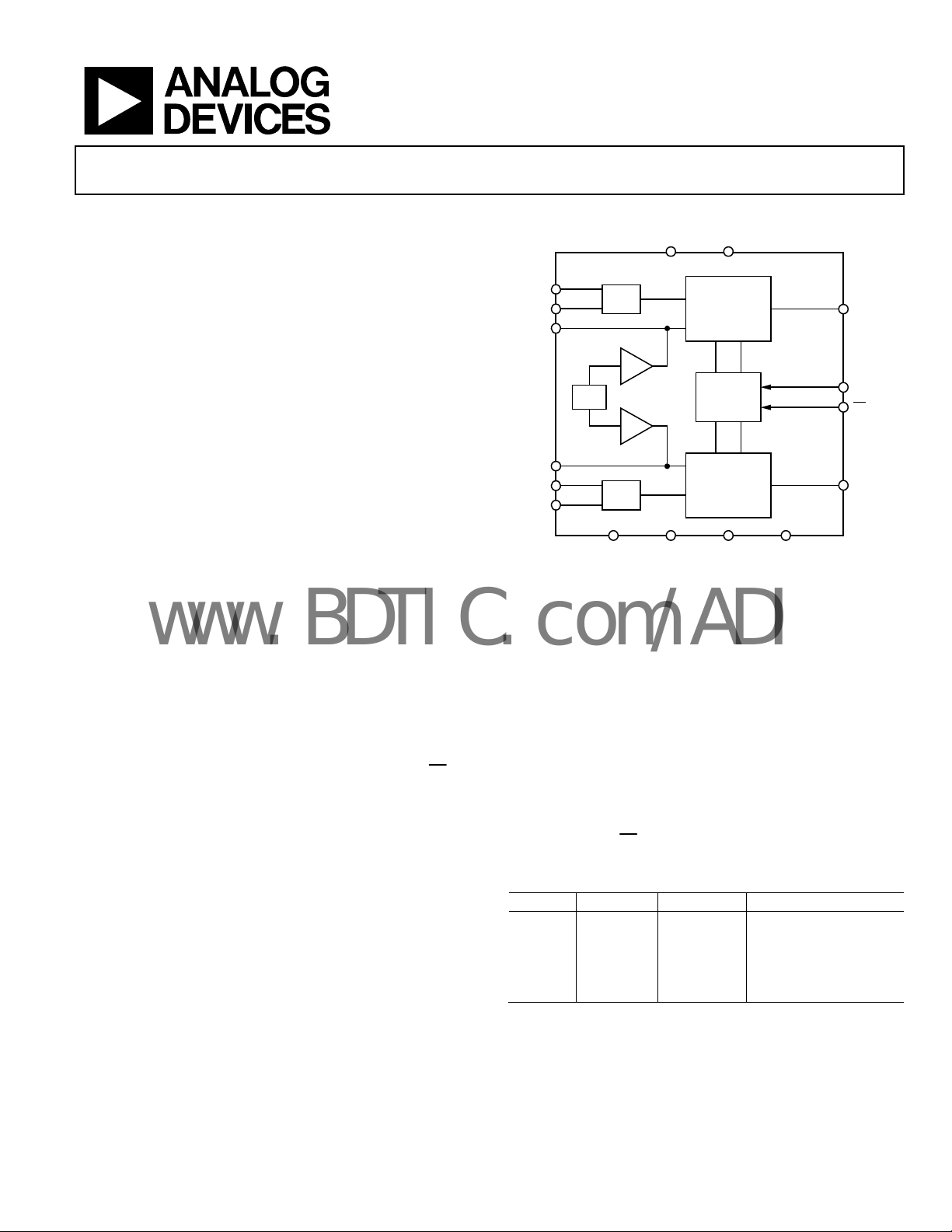
FUNCTIONAL BLOCK DIAGRAM
DRIVE
12-BIT
SUCCESSIVE
APPROXIMATION
ADC
CONTROL
LOGIC
12-BIT
SUCCESSIVE
APPROXIMATION
ADC
Figure 1.
AD7356
SDATA
SCLK
CS
SDATA
06505-001
DGNDREFGNDAGND
V
V
REF
REF
V
V
INA+
INA–
INB+
INB–
DD
T/H
A
BUF
REF
BUF
B
T/H
AGND
B
GENERAL DESCRIPTION
The AD73561 is a dual, 12-bit, high speed, low power, successive
approximation ADC that operates from a single 2.5 V power
supply and features throughput rates up to 5 MSPS. The part
contains two ADCs, each preceded by a low noise, wide bandwidth track-and-hold circuit that can handle input frequencies
in excess of 110 MHz.
The conversion process and data acquisition use standard
control inputs allowing for easy interfacing to microprocessors
or DSPs. The input signal is sampled on the falling edge of
a conversion is also initiated at this point. The conversion time
is determined by the SCLK frequency.
The AD7356 uses advanced design techniques to achieve very
low power dissipation at high throughput rates. With a 2.5 V
supply and a 5 MSPS throughput rate, the part consumes typically
14 mA. The part also offers a flexible power/throughput rate
management option.
The analog input range for the part is the differential common
mode ±V
/2. The AD7356 has an on-chip 2.048 V reference
REF
that can be overdriven when an external reference is preferred.
The AD7356 is available in a 16-lead thin shrink small outline
package (TSSOP).
CS
;
PRODUCT HIGHLIGHTS
1. Two Complete A D C Fu nc tions.
These functions allow simultaneous sampling and
conversion of two channels. The conversion result of both
channels is simultaneously available on separate data lines
or in succession on one data line if only one serial port is
available.
2. High Throughput with Low Power Consumption.
The AD7356 offers a 5 MSPS throughput rate with 36 mW
power consumption.
3. No Conversion Latency.
The AD7356 features two standard successive approximation ADCs with accurate control of the sampling
instant via a
Table 1. Related Devices
Generic Resolution Throughput Analog Input
AD7352 12-bit 3 MSPS Differential
AD7266 12-bit 2 MSPS Differential/single ended
AD7866 12-bit 1 MSPS Single-ended
AD7366 12-bit 1 MSPS Single-ended bipolar
AD7367 14-bit 1 MSPS Single-ended bipolar
CS
input and, once off, conversion control.
1
Protected by U.S. Patent No. 6,681,332.
Rev. 0
Information furnished by Analog Devices is believed to be accurate and reliable. However, no
responsibility is assumed by Anal og Devices for its use, nor for any infringements of p atents or other
rights of third parties that may result from its use. Specifications subject to change without notice. No
license is granted by implication or otherwise under any patent or patent rights of Analog Devices.
Trademarks and registered trademarks are the property of their respective owners.
One Technology Way, P.O. Box 9106, Norwood, MA 02062-9106, U.S.A.
Tel: 781.329.4700 www.analog.com
Fax: 781.461.3113 ©2008 Analog Devices, Inc. All rights reserved.

AD7356
www.BDTIC.com/ADI
TABLE OF CONTENTS
Features .............................................................................................. 1
Functional Block Diagram .............................................................. 1
General Description ......................................................................... 1
Product Highlights ........................................................................... 1
Revision History ............................................................................... 2
Specifications ..................................................................................... 3
Timing Specifications .................................................................. 5
Absolute Maximum Ratings ............................................................ 6
ESD Caution .................................................................................. 6
Pin Configuration and Function Descriptions ............................. 7
Typical Performance Characteristics ............................................. 8
Terminology .................................................................................... 10
Theory of Operation ...................................................................... 12
Circuit Information .................................................................... 12
Converter Operation .................................................................. 12
Analog Input Structure .............................................................. 12
Analog Inputs ............................................................................. 13
Driving Differential Inputs ....................................................... 14
ADC Transfer Function ............................................................. 14
Modes of Operation ....................................................................... 15
Normal Mode .............................................................................. 15
Partial Power-Down Mode ....................................................... 15
Full Power-Down Mode ............................................................ 16
Power-Up Times ......................................................................... 17
Power vs. Throughput Rate ....................................................... 17
Serial Interface ................................................................................ 18
Application Hints ........................................................................... 19
Grounding and Layout .............................................................. 19
Evaluating the AD7356 Performance ...................................... 19
Outline Dimensions ....................................................................... 20
Ordering Guide .......................................................................... 20
REVISION HISTORY
10/08—Revision 0: Initial Version
Rev. 0 | Page 2 of 20

AD7356
www.BDTIC.com/ADI
SPECIFICATIONS
IN+
MAX
and
IN+
and V
1
, unless
are
IN−
VDD = 2.5 V ± 10%, V
= 2.25 V to 3.6 V, internal reference = 2.048 V, f
DRIVE
= 80 MHz, f
SCLK
= 5 MSPS, TA = T
SAMPLE
MIN
to T
otherwise noted.
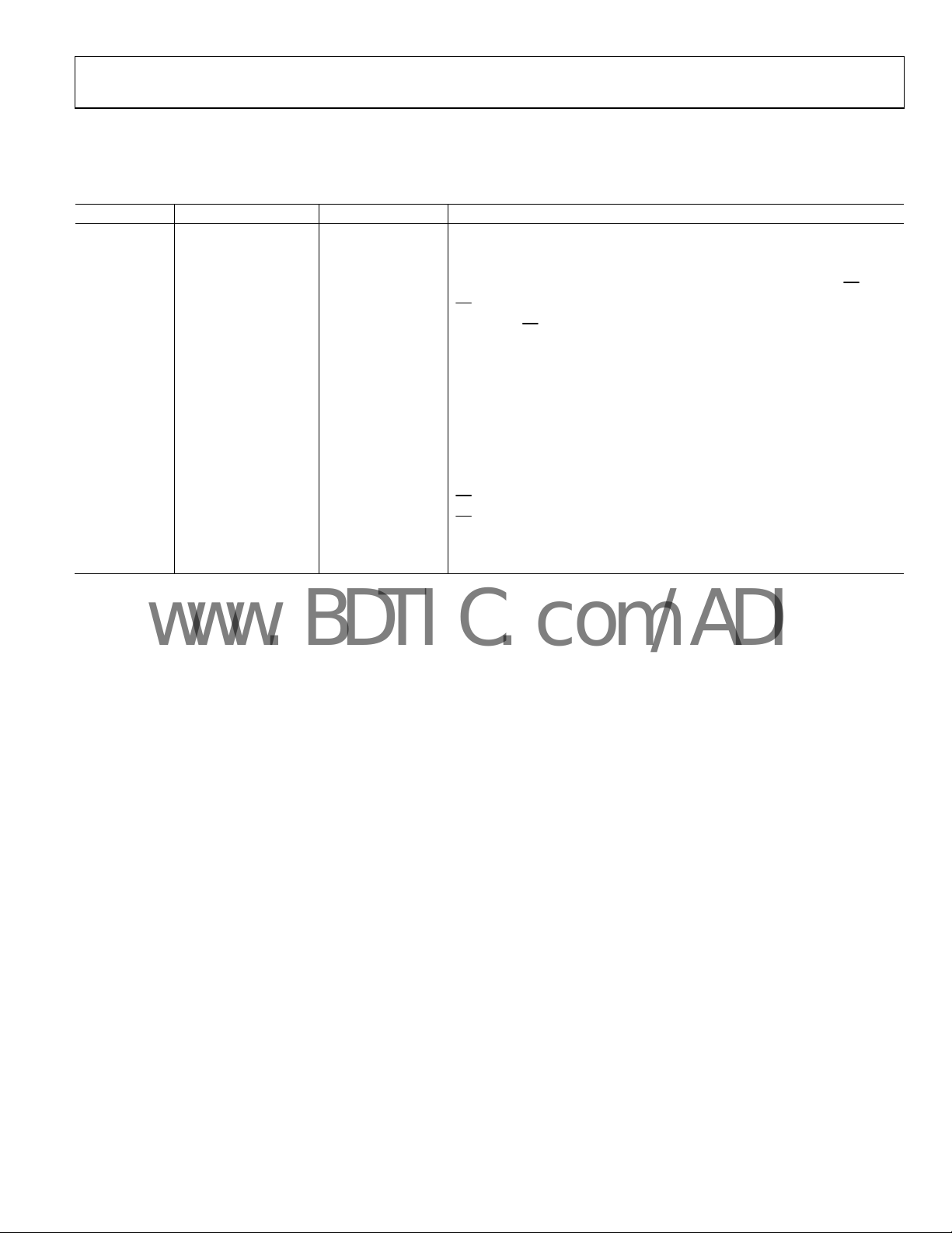
Table 2.
Parameter Min Typ Max Unit Test Conditions/Comments
DYNAMIC PERFORMANCE fIN = 1 MHz sine wave
Signal-to-Noise Ratio (SNR)
Signal-to-(Noise and Distortion) (SINAD)
Total Harmonic Distortion (THD)
Spurious Free Dynamic Range (SFDR)
Intermodulation Distortion (IMD)
Second-Order Terms −84 dB
Third-Order Terms −76 dB
ADC-to-ADC Isolation
2
CMRR
SAMPLE AND HOLD
Aperture Delay 3.5 ns
Aperture Delay Match 40 ps
Aperture Jitter 16 ps
Full Power Bandwidth
@ 3 dB 110 MHz
@ 0.1 dB 77 MHz
DC ACCURACY
Resolution 12 Bits
Integral Nonlinearity (INL)
Differential Nonlinearity (DNL)
Positive Full-Scale Error
Positive Full-Scale Error Match
Midscale Error
2
Midscale Error Match
Negative Full-Scale Error
Negative Full-Scale Error Match
ANALOG INPUT
Fully Differential Input Range (V
Common-Mode Voltage Range 0.5 1.9 V The voltage around which V
DC Leakage Current ±0.5 ±5 A
Input Capacitance 32 pF When in track mode
8 pF When in hold mode
REFERENCE INPUT/OUTPUT
V
Input Voltage Range 2.048 + 0.1 VDD V
REF
V
Input Current 0.3 0.45 mA When in reference overdrive mode
REF
V
Output Voltage 2.038 2.058 V 2.048 V ± 0.5% max @ VDD = 2.5 V ± 5%
REF
2.043 2.053 V 2.048 V ± 0.25% max @ VDD = 2.5 V ± 5% and 25°C
V
Temperature Coefficient 6 20 ppm/°C
REF
V
Long Term Stability 100 ppm For 1000 hours
REF
V
Thermal Hysteresis
REF
V
Noise 60 V rms
REF
V
Output Impedance 1 Ω
REF
2
2
2
2
2
2
2
2
2
70 71.5 dB
2
69.5 71 dB
−84 −77.5 dB
−85 −78.5 dB
fa = 1 MHz + 50 kHz, fb = 1 MHz − 50 KHz
−100 dB fIN = 1 MHz, f
−100 dB f
= 100 kHz to 2.5 MHz
NOISE
= 100 kHz to 2.5 MHz
NOISE
±0.5 ±1 LSB
±0.5 ±0.99 LSB Guaranteed no missed codes to 12 bits
±1 ±6 LSB
±2 ±8 LSB
+5 0/+11 LSB
2
2
2
and V
IN+
±2 ±8 LSB
±1 ±6 LSB
±2 ±8 LSB
) VCM ± V
IN−
/2 V VCM = common-mode voltage, V
REF
must remain within GND and VDD
V
IN−
centered
2
50 ppm
Rev. 0 | Page 3 of 20

AD7356
www.BDTIC.com/ADI
Parameter Min Typ Max Unit Test Conditions/Comments
LOGIC INPUTS
Input High Voltage (V
Input Low Voltage (V
Input Current (I
Input Capacitance (CIN) 3 pF
LOGIC OUTPUTS
Output High Voltage (VOH) V
Output Low Voltage (VOL) 0.2 V
Floating-State Leakage Current ±1 A
Floating-State Output Capacitance 5.5 pF
Output Coding Straight binary
CONVERSION RATE
Conversion Time t2 + 13 × t
Track-and-Hold Acquisition Time
Throughput Rate 5 MSPS
POWER REQUIREMENTS
VDD 2.25 2.75 V Nominal VDD = 2.5 V
V
2.25 3.6 V
DRIVE
4
I
TOTAL
Normal Mode (Operational) 14 20 mA
Normal Mode (Static) 6 7.8 mA SCLK on or off
Partial Power-Down Mode 3.5 4.5 mA SCLK on or off
Full Power-Down Mode 5 40 A SCLK on or off, −40°C to +85°C
90 A SCLK on or off, 85°C to 125°C
Power Dissipation
Normal Mode (Operational) 36 59 mW
Normal Mode (Static) 16 21.5 mW SCLK on or off
Partial Power-Down Mode 9.5 11.5 mW SCLK on or off
Full Power-Down Mode 16 110 W SCLK on or off, −40°C to +85°C
250 W SCLK on or off, 85°C to 125°C
1
Temperature ranges are as follows: Y Grade: −40°C to +125°C; B Grade: −40°C to +85°C.
2
See the Terminology section.
3
Current and power typical specifications are based on results with VDD = 2.5 V and V
4
I
is the total current flowing in VDD and V
TOTAL
) 0.6 × V
INH
) 0.3 × V
INL
) ±1 A VIN = 0 V or V
IN)
2
3
30 ns Full-scale step input, settling to 0.5 LSBs
V
DRIVE
V
DRIVE
− 0.2 V
DRIVE
ns
SCLK
Digital inputs = 0 V or V
= 3.0 V.
DRIVE
.
DRIVE
DRIVE
DRIVE
Rev. 0 | Page 4 of 20

AD7356
www.BDTIC.com/ADI
TIMING SPECIFICATIONS
VDD = 2.5 V ± 10%, V
= 2.25 V to 3.6 V, internal reference = 2.048 V, TA = T
DRIVE
MAX
Table 3.
Parameter Limit at T
f
SCLK
50 kHz min
MIN
, T
MAX
Unit Description
80 MHz max
t
CONVER T
t
5 ns min
QUIET
t
2
2
t
3
2, 3
t
4
12.5 ns max 1.8 V ≤ V
11 ns max 2.25 V ≤ V
9.5 ns max 2.75 V ≤ V
9 ns max 3.3 V ≤ V
t2 + 13 × t
ns max t
SCLK
SCLK
= 1/f
SCLK
Minimum time between end of serial read and next falling edge of CS
5 ns min
6 ns max
to SCLK setup time
CS
Delay from CS
until SDATAA and SDATAB are three-state disabled
Data access time after SCLK falling edge
< 2.25 V
DRIVE
< 2.75 V
DRIVE
< 3.3 V
DRIVE
≤ 3.6 V
DRIVE
t5 5 ns min SCLK low pulse width
t6 5 ns min SCLK high pulse width
2
t
3.5 ns min SCLK to data valid hold time
7
2
t
9.5 ns max
8
t9 5 ns min
2
t
4.5 ns min SCLK falling edge to SDATA
10
rising edge to SDATA , SDATAB high impedance
CS
rising edge to falling edge pulse width
CS
9.5 ns max SCLK falling edge to SDATAA, SDATAB high impedance
1
Temperature ranges are as follows: Y Grade: −40°C to +125°C; B Grade: −40°C to +85°C.
2
Specified with a load capacitance of 10 pF on SDATAA and SDATAB.
3
The time required for the output to cross 0.4 V or 2.4 V.
1
to T
, unless otherwise noted.
MIN
A
, SDATAB high impedance
A
Rev. 0 | Page 5 of 20

AD7356
www.BDTIC.com/ADI
ABSOLUTE MAXIMUM RATINGS
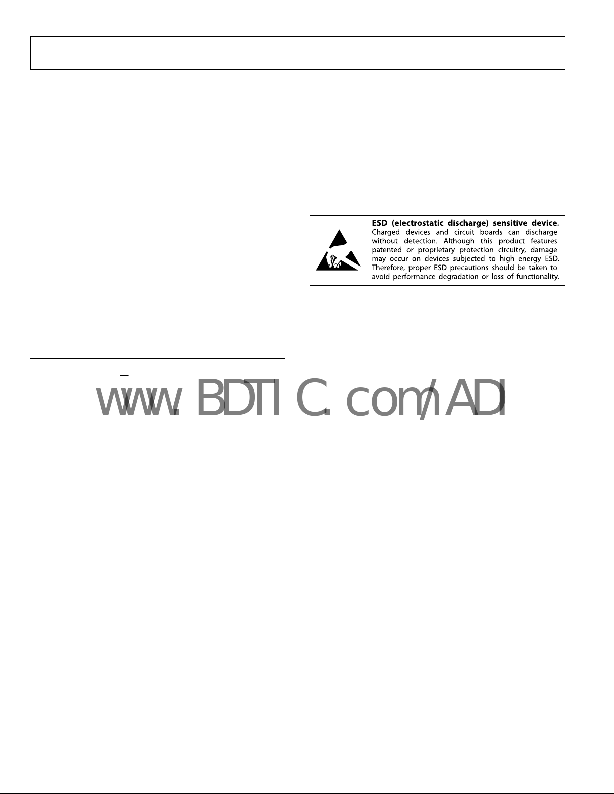
Table 4.
Parameter Rating
VDD to AGND, DGND, REFGND
V
to AGND, DGND, REFGND −0.3 V to +5 V
DRIVE
VDD to V
AGND to DGND to REFGND
Analog Input Voltages1 to AGND
Digital Input Voltages2 to DGND −0.3 V to V
Digital Output Voltages3 to DGND
Input Current to Any Pin Except Supply Pins4 ±10 mA
Operating Temperature Range
Y Grade
B Grade
Storage Temperature Range
Junction Temperature 150°C
TSSOP
θJA Thermal Impedance 143°C/W
θJC Thermal Impedance 45°C/W
Lead Temperature, Soldering
Reflow Temperature (10 sec to 30 sec) 255°C
ESD 1.5 kV
1
Analog input voltages are V
2
Digital input voltages are CS and SCLK.
3
Digital output voltages are SDATAA and SDATAB.
4
Transient currents of up to 100 mA do not cause SCR latch-up.
−5 V to +3 V
DRIVE
, V
, V
INA−
INB+
, V
INA+
−0.3 V to +3 V
−0.3 V to +0.3 V
−0.3 V to V
−0.3 V to V
−40°C to +125°C
−40°C to +85°C
−65°C to +150°C
, REFA, and REFB.
INB−
+ 0.3 V
DD
+ 0.3 V
DRIVE
+ 0.3 V
DRIVE
Stresses above those listed under Absolute Maximum Ratings
may cause permanent damage to the device. This is a stress
rating only; functional operation of the device at these or any
other conditions above those indicated in the operational
section of this specification is not implied. Exposure to absolute
maximum rating conditions for extended periods may affect
device reliability.
ESD CAUTION
Rev. 0 | Page 6 of 20
 Loading...