REV. C
Information furnished by Analog Devices is believed to be accurate and
reliable. However, no responsibility is assumed by Analog Devices for its
use, nor for any infringements of patents or other rights of third parties
which may result from its use. No license is granted by implication or
otherwise under any patent or patent rights of Analog Devices.
a
AD734
One Technology Way, P.O. Box 9106, Norwood, MA 02062-9106, U.S.A.
Tel: 781/329-4700 World Wide Web Site: http://www.analog.com
Fax: 781/326-8703 © Analog Devices, Inc., 1999
10 MHz, 4-Quadrant
Multiplier/Divider
FEATURES
High Accuracy
0.1% Typical Error
High Speed
10 MHz Full-Power Bandwidth
450 V/s Slew Rate
200 ns Settling to 0.1% at Full Power
Low Distortion
–80 dBc from Any Input
Third-Order IMD Typically –75 dBc at 10 MHz
Low Noise
94 dB SNR, 10 Hz to 20 kHz
70 dB SNR, 10 Hz to 10 MHz
Direct Division Mode
2 MHz BW at Gain of 100
APPLICATIONS
High Performance Replacement for AD534
Multiply, Divide, Square, Square Root
Modulator, Demodulator
Wideband Gain Control, RMS-DC Conversion
Voltage-Controlled Amplifiers, Oscillators, and Filters
Demodulator with 40 MHz Input Bandwidth
demodulator with input frequencies as high as 40 MHz as long
as the desired output frequency is less than 10 MHz.
The AD734AQ and AD734BQ are specified for the industrial
temperature range of –40°C to +85°C and come in a 14-lead
ceramic DIP. The AD734SQ/883B, available processed to
MIL-STD-883B for the military range of –55°C to +125°C, is
available in a 14-lead ceramic DIP.
PRODUCT HIGHLIGHTS
The AD734 embodies more than two decades of experience in
the design and manufacture of analog multipliers, to provide:
1. A new output amplifier design with more than twenty times
the slew-rate of the AD534 (450 V/µs versus 20 V/µs) for a
full power (20 V pk-pk) bandwidth of 10 MHz.
2. Very low distortion, even at full power, through the use of
circuit and trimming techniques that virtually eliminate all of
the spurious nonlinearities found in earlier designs.
3. Direct control of the denominator, resulting in higher
multiplier accuracy and a gain-bandwidth product at small
denominator values that is typically 200 times greater than
that of the AD534 in divider modes.
4. Very clean transient response, achieved through the use of a
novel input stage design and wide-band output amplifier,
which also ensure that distortion remains low even at high
frequencies.
5. Superior noise performance by careful choice of device
geometries and operating conditions, which provide a
guaranteed 88 dB of dynamic range in a 20 kHz bandwidth.
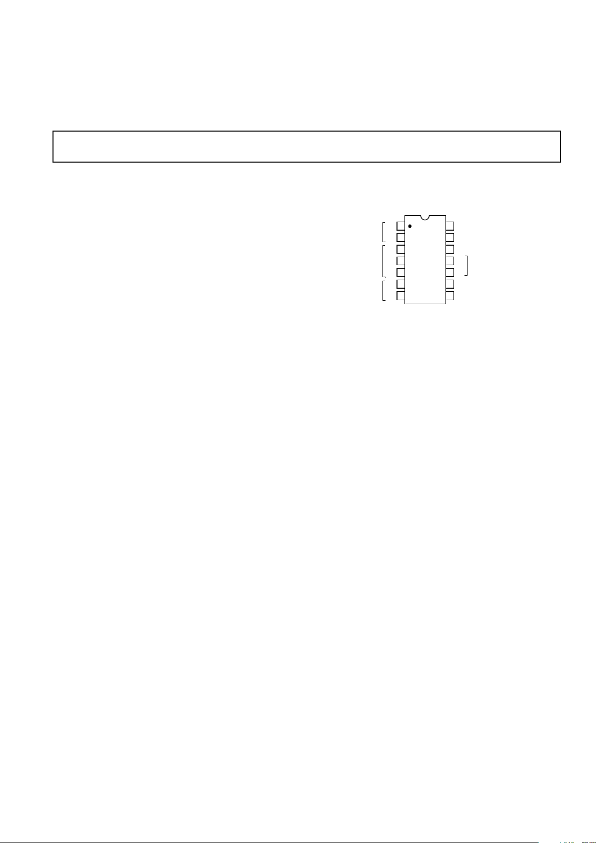
CONNECTION DIAGRAM
14-Lead DIP
(Q Package and N Package)
14
13
12
11
10
9
8
1
2
3
4
7
6
5
TOP VIEW
(Not to Scale)
X1
Z1
W OUTPUT
DD DENOMINATOR DISABLE
VP POSITIVE SUPPLY
X2
U0
U1
AD734
VN NEGATIVE SUPPLY
ER REFERENCE VOLTAGE
Z2
U2
Y1
Y2
Z INPUT
X INPUT
DENOMINATOR
INTERFACE
Y INPUT
PRODUCT DESCRIPTION
The AD734 is an accurate high speed, four-quadrant analog
multiplier that is pin-compatible with the industry-standard
AD534 and provides the transfer function W = XY/U. The
AD734 provides a low-impedance voltage output with a fullpower (20 V pk-pk) bandwidth of 10 MHz. Total static error
(scaling, offsets, and nonlinearities combined) is 0.1% of full
scale. Distortion is typically less than –80 dBc and guaranteed.
The low capacitance X, Y and Z inputs are fully differential. In
most applications, no external components are required to
define the function.
The internal scaling (denominator) voltage U is 10 V, derived
from a buried-Zener voltage reference. A new feature provides
the option of substituting an external denominator voltage,
allowing the use of the AD734 as a two-quadrant divider with a
1000:1 denominator range and a signal bandwidth that remains
10 MHz to a gain of 20 dB, 2 MHz at a gain of 40 dB and
200 kHz at a gain of 60 dB, for a gain-bandwidth product of
200 MHz.
The advanced performance of the AD734 is achieved by a
combination of new circuit techniques, the use of a high speed
complementary bipolar process and a novel approach to lasertrimming based on ac signals rather than the customary dc
methods. The wide bandwidth (>40 MHz) of the AD734’s
input stages and the 200 MHz gain-bandwidth product of the
multiplier core allow the AD734 to be used as a low distortion

–2–
REV. C
AD734–SPECIFICATIONS
TRANSFER FUNCTION
W = A
O
X
1−X2
()
Y
1−Y2
()
U
1−U2
()
− Z1−Z
2
()
ABS
Parameter Conditions Min Typ Max Min Typ Max Min Typ Max Units
MULTIPLIER PERFORMANCE
Transfer Function W = XY/10 W = XY/10 W = XY/10
Total Static Error
1
–10 V ≤ X, Y ≤ 10 V 0.1 0.4 0.1 0.25 0.1 0.4 %
Over T
MIN
to T
MAX
1 0.6 1.25 %
vs. Temperature T
MIN
to T
MAX
0.004 0.003 0.004 %/°C
vs. Either Supply ±V
S
= 14 V to 16 V 0.01 0.05 0.01 0.05 0.01 0.05 %/V
Peak Nonlinearity –10 V ≤ X ≤ +10 V, Y = +10 V 0.05 0.05 0.05 %
–10 V ≤ Y ≤ +10 V, X = +10 V 0.025 0.025 0.025 %
THD
2
X = 7 V rms, Y = +10 V, f ≤ 5 kHz –58 –66 –58 dBc
T
MIN
to T
MAX
–55 –63 –55 dBc
Y = 7 V rms, X = +10 V, f ≤ 5 kHz –60 –80 –60 dBc
T
MIN
to T
MAX
–57 –74 –57 dBc
Feedthrough X = 7 V rms, Y = nulled, f ≤ 5 kHz –85 –60 –85 –70 –85 –60 dBc
Y = 7 V rms, X = nulled, f ≤ 5 kHz –85 –66 –85 –76 –85 –66 dBc
Noise (RTO) X = Y = 0
Spectral Density 100 Hz to 1 MHz 1.0 1.0 1.0 µV/√Hz
Total Output Noise 10 Hz to 20 kHz –94 –88 –94 –88 –94 –88 dBc
T
MIN
to T
MAX
–85 –85 –85 dBc
DIVIDER PERFORMANCE (Y = 10 V)
Transfer Function W = XY/U W = XY/U W = XY/U
Gain Error Y = 10 V, U = 100 mV to 10 V 1 1 1 %
X Input Clipping Level Y ≤ 10 V 1.25 × U 1.25 × U 1.25 × UV
U Input Scaling Error
3
0.3 0.15 0.3 %
T
MIN
to T
MAX
0.8 0.65 1 %
(Output to 1%) U = 1 V to 10 V Step, X = 1 V 100 100 100 ns
INPUT INTERFACES (X, Y, & Z)
3 dB Bandwidth 40 40 40 MHz
Operating Range Differential or Common Mode ±12.5 ±12.5 ±12.5 V
X Input Offset Voltage 15 5 15 mV
T
MIN
to T
MAX
25 15 25 mV
Y Input Offset Voltage 10 5 10 mV
T
MIN
to T
MAX
12 6 12 mV
Z Input Offset Voltage 20 10 20 mV
T
MIN
to T
MAX
50 50 90 mV
Z Input PSRR (Either Supply) f ≤ 1 kHz 54 70 66 70 54 70 dB
T
MIN
to T
MAX
50 56 50 dB
CMRR f = 5 kHz 70 85 70 85 70 85 dB
Input Bias Current (X, Y, Z Inputs) 50 300 50 150 50 300 nA
T
MIN
to T
MAX
400 300 500 nA
Input Resistance Differential 50 50 50 kΩ
Input Capacitance Differential 2 2 2 pF
DENOMINATOR INTERFACES (U0, U1, & U2)
Operating Range VN to VP-3 VN to VP-3 VN to VP-3 V
Denominator Range 1000:1 1000:1 1000:1
Interface Resistor U1 to U2 28 28 28 kΩ
OUTPUT AMPLIFIER (W)
Output Voltage Swing T
MIN
to T
MAX
±12 ±12 ±12 V
Open-Loop Voltage Gain X = Y = 0, Input to Z 72 72 72 dB
Dynamic Response From X or Y Input, CL ≤ 20 pF
3 dB Bandwidth W ≤ 7 V rms 8 10 8 10 8 10 MHz
Slew Rate 450 450 450 V/µs
Settling Time +20 V or –20 V Output Step
To 1% 125 125 125 ns
To 0.1% 200 200 200 ns
Short-Circuit Current T
MIN
to T
MAX
20 50 80 20 50 80 20 50 80 mA
POWER SUPPLIES, ±V
S
Operating Supply Range ±8 ±16.5 ±8 ±16.5 ±8 ±16.5 V
Quiescent Current T
MIN
to T
MAX
6912 6912 6912 mA
NOTES
1
Figures given are percent of full scale (e.g., 0.01% = 1 mV).
2
dBc refers to deciBels relative to the full-scale input (carrier) level of 7 V rms.
3
See Figure 10 for test circuit.
All min and max specifications are guaranteed.
Specifications subject to change without notice.
(TA = +25ⴗC, +VS = VP = +15 V, –VS = VN = –15 V, R
L
≥ 2 k⍀)

AD734
–3–
REV. C
ABSOLUTE MAXIMUM RATINGS
1
Supply Voltage . . . . . . . . . . . . . . . . . . . . . . . . . . . . . . . . ±18 V
Internal Power Dissipation
2
for T
J
max = 175°C . . . . . . . . . . . . . . . . . . . . . . . . 500 mW
X, Y and Z Input Voltages . . . . . . . . . . . . . . . . . . . . VN to VP
Output Short Circuit Duration . . . . . . . . . . . . . . . . Indefinite
Storage Temperature Range
Q . . . . . . . . . . . . . . . . . . . . . . . . . . . . . . . –65°C to +150°C
Operating Temperature Range
AD734A, B (Industrial) . . . . . . . . . . . . . . . –40°C to +85°C
AD734S (Military) . . . . . . . . . . . . . . . . . . –55°C to +125°C
Lead Temperature Range (soldering 60 sec) . . . . . . . . +300°C
Transistor Count . . . . . . . . . . . . . . . . . . . . . . . . . . . . . . . . . 81
ESD Rating . . . . . . . . . . . . . . . . . . . . . . . . . . . . . . . . . . 500 V
NOTES
1
Stresses above those listed under Absolute Maximum Ratings may cause permanent damage to the device. This is a stress rating only; functional operation of the
device at these or any other conditions above those indicated in the operational
section of this specification is not implied.
2
14-Lead Ceramic DIP: θ
JA
= 110°C/W.
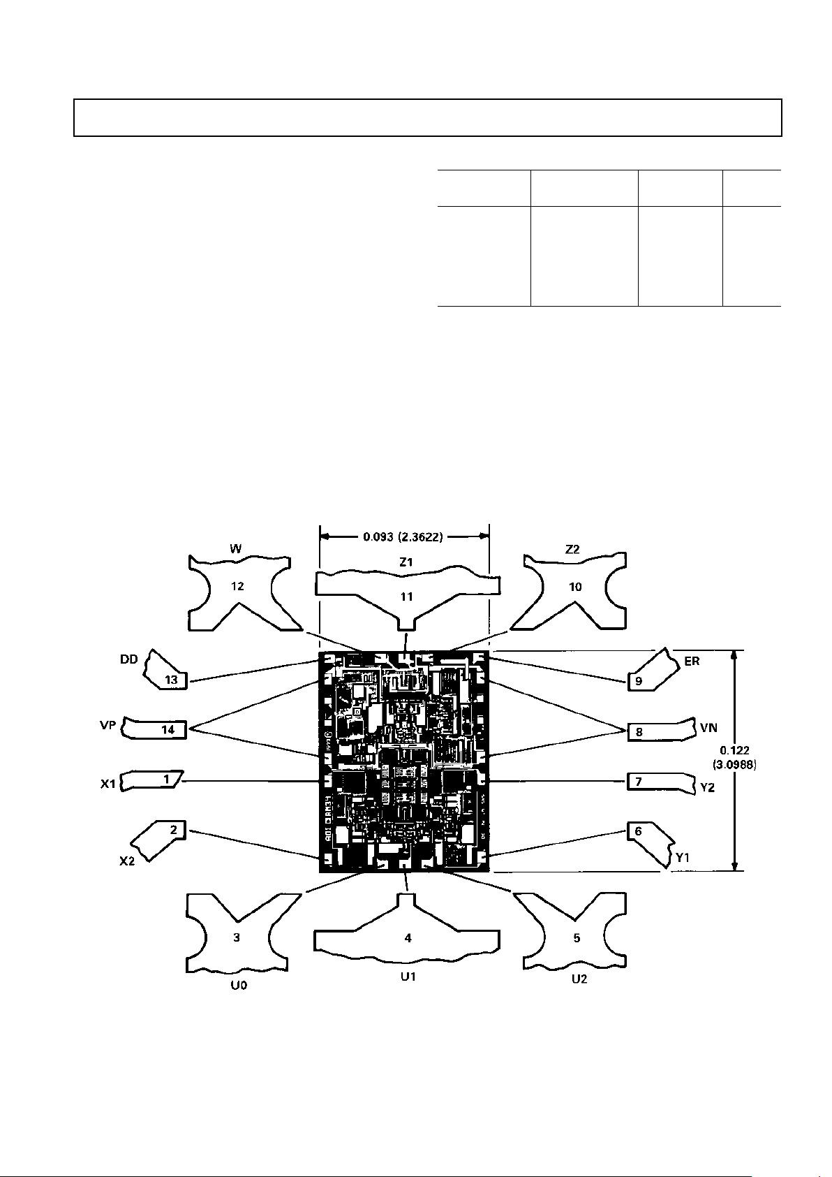
CHIP DIMENSIONS & BONDING DIAGRAM
Dimensions shown in inches and (mm).
(Contact factory for latest dimensions.)
ORDERING GUIDE
Temperature Package Package
Model Range Description Option
AD734AN –40°C to +85°C Plastic DIP N-14
AD734BN –40°C to +85°C Plastic DIP N-14
AD734AQ –40°C to +85°C Cerdip Q-14
AD734BQ –40°C to +85°C Cerdip Q-14
AD734SQ/883B –55°C to +125°C Cerdip Q-14
AD734SCHIPS –55°C to +125°CDie

AD734
–4–
REV. C
is typically less than 5 mV, which corresponds to a bias current
of only 100 nA. This low bias current ensures that mismatches
in the sources resistances at a pair of inputs does not cause an
offset error. These currents remain low over the full temperature
range and supply voltages.
The common-mode range of the X, Y and Z inputs does not
fully extend to the supply rails. Nevertheless, it is often possible
to operate the AD734 with one terminal of an input pair connected to either the positive or negative supply, unlike previous
multipliers. The common-mode resistance is several megohms.
The full-scale output of ±10 V can be delivered to a load resistance of 1 kΩ (although the specifications apply to the standard
multiplier load condition of 2 kΩ). The output amplifier is
stable driving capacitive loads of at least 100 pF, when a slight
increase in bandwidth results from the peaking caused by this
capacitance. The 450 V/µs slew rate of the AD734’s output am-
plifier ensures that the bandwidth of 10 MHz can be maintained
up to the full output of 20 V pk-pk. Operation at reduced supply
voltages is possible, down to ±8 V, with reduced signal levels.
Available Transfer Functions
The uncommitted (open-loop) transfer function of the AD734 is
W = A
O
X
1
− X
2
()
Y
1−Y2
()
U
− Z1− Z
2
()
, (1)
where A
O
is the open-loop gain of the output op-amp, typically
72 dB. When a negative feedback path is provided, the circuit
will force the quantity inside the brackets essentially to zero,
resulting in the equation
(X
1
– X2)(Y1 – Y2) = U (Z1 – Z2) (2)
This is the most useful generalized transfer function for the
AD734; it expresses a balance between the product XY and the
product UZ. The absence of the output, W, in this equation
only reflects the fact that we have not yet specified which of the
inputs is to be connected to the op amp output.
Most of the functions of the AD734 (including division, unlike
the AD534 in this respect) are realized with Z
1
connected to W.
So, substituting W in place of Z
1
in the above equation results in
an output.
W =
X
1
− X
2
()
Y
1−Y2
()
U
+ Z
2
.
(3)
The free input Z2 can be used to sum another signal to the
output; in the absence of a product signal, W simply follows the
voltage at Z2 with the full 10 MHz bandwidth. When not
needed for summation, Z2 should be connected to the ground
associated with the load circuit. We can show the allowable
polarities in the following shorthand form:
±W
()
=
±X
()
±Y
()
+U
()
+±Z.
(4)
In the recommended direct divider mode, the Y input is set to a
fixed voltage (typically 10 V) and U is varied directly; it may
have any value from 10 mV to 10 V. The magnitude of the ratio
X/U cannot exceed 1.25; for example, the peak X-input for U
= 1 V is ±1.25 V. Above this level, clipping occurs at the
positive and negative extremities of the X-input. Alternatively,
Ru
DENOMINATOR
CONTROL
DD
ER
∑
XY/U – Z
∞
HIGH-ACCURACY
TRANSLINER
MULTIPLIER CORE
AD734
X1
X2
U0
U1
U2
Y1
Y2
W
Z1
Z2
U
X = X1 – X
2
Y = Y1 – Y
2
Z = Z1 – Z
2
WIF
ZIF
A
O
XIF
YIF
XZ
U
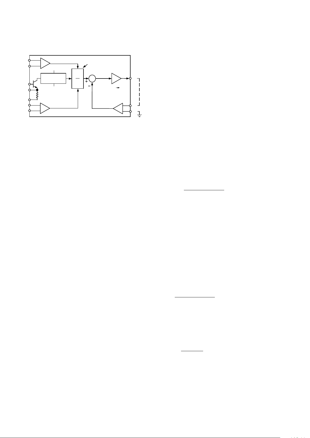
Figure 1. AD734 Block Diagram
FUNCTIONAL DESCRIPTION
Figure 1 is a simplified block diagram of the AD734. Operation
is similar to that of the industry-standard AD534 and in many
applications these parts are pin-compatible. The main functional
difference is the provision for direct control of the denominator
voltage, U, explained fully on the following page. Internal signals are actually in the form of currents, but the function of the
AD734 can be understood using voltages throughout, as shown
in this figure. Pins are named using upper-case characters (such
as X1, Z2) while the voltages on these pins are denoted by subscripted variables (for example, X
1
, Z2).
The AD734’s differential X, Y and Z inputs are handled by
wideband interfaces that have low offset, low bias current and
low distortion. The AD734 responds to the difference signals
X = X
1
– X2, Y = Y1 – Y2 and Z = Z1 – Z2, and rejects
common-mode voltages on these inputs. The X, Y and Z
interfaces provide a nominal full-scale (FS) voltage of ±10 V,
but, due to the special design of the input stages, the linear
range of the differential input can be as large as ±17 V. Also
unlike previous designs, the response on these inputs is not
clipped abruptly above ±15 V, but drops to a slope of one half.
The bipolar input signals X and Y are multiplied in a translinear
core of novel design to generate the product XY/U. The
denominator voltage, U, is internally set to an accurate,
temperature-stable value of 10 V, derived from a buried-Zener
reference. An uncalibrated fraction of the denominator voltage
U appears between the voltage reference pin (ER) and the
negative supply pin (VN), for use in certain applications where
a temperature-compensated voltage reference is desirable. The
internal denom-inator, U, can be disabled, by connecting the
denominator disable Pin 13 (DD) to the positive supply pin
(VP); the denom-inator can then be replaced by a fixed or
variable external volt-age ranging from 10 mV to more than 10 V.
The high-gain output op-amp nulls the difference between
XY/U and an additional signal Z, to generate the final output
W. The actual transfer function can take on several forms, depending on the connections used. The AD734 can perform all
of the functions supported by the AD534, and new functions
using the direct-division mode provided by the U-interface.
Each input pair (X1 and X2, Y1 and Y2, Z1 and Z2) has a
differential input resistance of 50 kΩ; this is formed by “real”
resistors (not a small-signal approximation) and is subject to a
tolerance of ±20%. The common-mode input resistance is
several megohms and the parasitic capacitance is about 2 pF.
The bias currents associated with these inputs are nulled by
laser-trimming, such that when one input of a pair is optionally
ac-coupled and the other is grounded, the residual offset voltage
 Loading...