Dual Low Power CMOS
a
Analog Front End with DSP Microcomputer
FEATURES
AFE PERFORMANCE
Two 16-Bit A/D Converters
Two 16-Bit D/A Converters
Programmable Input/Output Sample Rates
78 dB ADC SNR
77 dB DAC SNR
64 kS/s Maximum Sample Rate
–90 dB Crosstalk
Low Group Delay (25 s Typ per ADC Channel,
50 s Typ per DAC Channel)
Programmable Input/Output Gain
On-Chip Reference
DSP PERFORMANCE
19 ns Instruction Cycle Time @ 3.3 V, 52 MIPS
Sustained Performance
Single-Cycle Instruction Execution
Single-Cycle Context Switch
3-Bus Architecture Allows Dual Operand Fetches in
Every Instruction Cycle
Multifunction Instructions
Power-Down Mode Featuring Low CMOS Standby
Power Dissipation with 400 Cycle Recovery from
Power-Down Condition
Low Power Dissipation in Idle Mode
GENERAL DESCRIPTION
The AD73422 is a single device incorporating a dual analog
front end and a microcomputer optimized for digital signal
processing (DSP) and other high speed numeric processing
applications.
The AD73422’s analog front end (AFE) section features a dual
front-end converter for general purpose applications including
speech and telephony. The AFE section features two 16-bit A/D
conversion channels and two 16-bit D/A conversion channels.
Each channel provides 77 dB signal-to-noise ratio over a
voiceband signal bandwidth. It also features an input-to-output
gain network in both the analog and digital domains. This is
featured on both codecs and can be used for impedance matching or scaling when interfacing to Subscriber Line Interface
Circuits (SLICs).
The AD73422 is particularly suitable for a variety of applications in the speech and telephony area including low bit rate,
high quality compression, speech enhancement, recognition
and synthesis. The low group delay characteristic of the AFE
makes it suitable for single or multichannel active control
AD73422
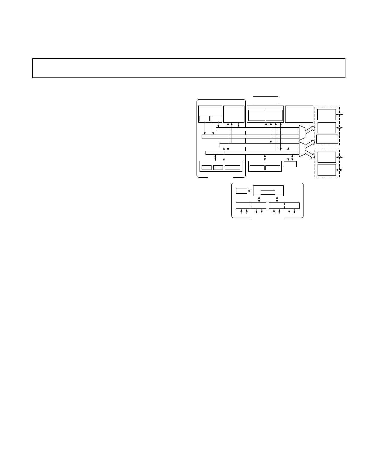
FUNCTIONAL BLOCK DIAGRAM
POWER-DOWN
CONTROL
DATA
ADDRESS
GENERATORS
DAG 2
DAG 1
ARITHMETIC UNITS
ADSP-2100 BASE
ARCHITECTURE
PROGRAM
SEQUENCER
PROGRAM MEMORY ADDRESS
DATA MEMORY ADDRESS
PROGRAM MEMORY DATA
DATA MEMORY DATA
SHIFTERMACALU
REF
MEMORY
16K DM
16K PM
(OPTIONAL
(OPTIONAL
SPORT 0
ANALOG FRONT END
8K)
SERIAL PORTS
SPORT 1
SERIAL PORT
SPORT 2
SECTION
8K)
ADC2 DAC2ADC1 DAC1
PROGRAMMABLE
I/O
AND
FLAGS
TIMER
applications. The A/D and D/A conversion channels feature
programmable input/output gains with ranges 38 dB and 21 dB
respectively. An on-chip reference voltage is included to allow
single supply operation.
The sampling rate of the AFE is programmable with four separate settings offering 64, 32, 16 and 8 kHz sampling rates (from
a master clock of 16.384 MHz), while the serial port (SPORT2)
allows easy expansion of the number of I/O channels by cascading extra AFEs external to the AD73422.
The AD73422’s DSP engine combines the ADSP-2100 family
base architecture (three computational units, data address generators and a program sequencer) with two serial ports, a 16-bit
internal DMA port, a byte DMA port, a programmable timer,
Flag I/O, extensive interrupt capabilities and on-chip program
and data memory.
The AD73422-80 integrates 80K bytes of on-chip memory
configured as 16K words (24-bit) of program RAM, and 16K
words (16-bit) of data RAM. The AD73422-40 integrates 40K
bytes of on-chip memory configured as 8K words (24-bit) of
program RAM, and 8K words (16-bit) of data RAM. Powerdown circuitry is also provided to meet the low power needs of
battery operated portable equipment. The AD73422 is available
in a 119-ball PBGA package.
FULL MEMORY
MODE
EXTERNAL
ADDRESS
BUS
EXTERNAL
DATA
BUS
BYTE DMA
CONTROLLER
OR
EXTERNAL
DATA
BUS
INTERNAL
DMA
PORT
HOST MODE
REV. 0
Information furnished by Analog Devices is believed to be accurate and
reliable. However, no responsibility is assumed by Analog Devices for its
use, nor for any infringements of patents or other rights of third parties
which may result from its use. No license is granted by implication or
otherwise under any patent or patent rights of Analog Devices.
One Technology Way, P.O. Box 9106, Norwood, MA 02062-9106, U.S.A.
Tel: 781/329-4700 World Wide Web Site: http://www.analog.com
Fax: 781/326-8703 © Analog Devices, Inc., 1999

AD73422–SPECIFICATIONS
(AVDD = DVDD = VDD = +3 V to 3.6 V; DGND = AGND = 0 V, f
f
= 64 kHz; TA = T
SAMP
MIN
to T
, unless otherwise noted.)
MAX
= 16.384 MHz,
DMCLK
Parameter Min Typ Max Units Test Conditions
AFE SECTION
REFERENCE
REFCAP
Absolute Voltage, V
REFCAP
1.125 1.25 1.375 V
REFCAP TC 50 ppm/°C 0.1 µF Capacitor Required from
REFOUT REFCAP to AGND2
Typical Output Impedance 130 Ω
Absolute Voltage, V
REFOUT
1.08 1.2 1.32 V Unloaded
Minimum Load Resistance 1 kΩ
Maximum Load Capacitance 100 pF
INPUT AMPLIFIER
Offset ± 1.0 mV
Maximum Output Swing 1.578 V Max Output Swing = (1.578/1.25) ×
V
REFCAP
Feedback Resistance 50 kΩ fC = 32 kHz
Feedback Capacitance 100 pF
ANALOG GAIN TAP
Gain at Maximum Setting +1
Gain at Minimum Setting –1
Gain Resolution 5 Bits Gain Step Size = 0.0625
Gain Accuracy ± 1.0 % Output Unloaded
Settling Time 1.0 ms Tap Gain Change of –FS to +FS
Delay 0.5 ms
ADC SPECIFICATIONS
Maximum Input Range at VIN
2, 3
1.578 V p-p Measured Differentially.
–2.85 dBm Max Input = (1.578/1.25) × V
REFCAP
Nominal Reference Level at VIN 1.0954 V p-p Measured Differentially
(0 dBm0) –6.02 dBm
Absolute Gain
PGA = 0 dB –0.5 0.4 +1.2 dB 1.0 kHz, 0 dBm0
PGA = 38 dB –0.7 dB 1.0 kHz, 0 dBm0
Gain Tracking Error ± 0.1 dB 1.0 kHz, +3 dBm0 to –50 dBm0
Signal to (Noise + Distortion)
PGA = 0 dB 72 78 dB 300 Hz to 3400 Hz; f
78 dB 300 Hz to 3400 Hz; f
55 57 dB 0 Hz to f
SAMP
/2; f
SAMP
PGA = 38 dB 56 dB 300 Hz to 3400 Hz; f
= 64 kHz
SAMP
= 8 kHz
SAMP
= 64 kHz
= 64 kHz
SAMP
Total Harmonic Distortion
PGA = 0 dB –84 –73 dB 300 Hz to 3400 Hz; f
PGA = 38 dB –70 dB 300 Hz to 3400 Hz; f
SAMP
SAMP
= 64 kHz
= 64 kHz
Intermodulation Distortion –65 dB PGA = 0 dB
Idle Channel Noise –71 dBm0 PGA = 0 dB
Crosstalk, ADC-to-DAC –100 dB ADC Input Level: 1.0 kHz, 0 dBm0
DAC Input at Idle
ADC-to-ADC –100 dB ADC1 Input Level: 1.0 kHz, 0 dBm0
ADC2 Input at Idle. Input Amps Bypassed
–70 dB Input Amplifiers Included in Input
Channel
DC Offset –30 +10 +45 mV PGA = 0 dB
Power Supply Rejection –65 dB Input Signal Level at AVDD and DVDD
Group Delay
4, 5
Input Resistance at PGA
2, 4, 6
25 µs
20 kΩ DMCLK = 16.384 MHz; Input
Pins: 1.0 kHz, 100 mV p-p Sine Wave
Amplifiers Bypassed and AGT Off
DIGITAL GAIN TAP
Gain at Maximum Setting +1
Gain at Minimum Setting –1
Gain Resolution 16 Bits Tested to 5 MSBs of Settings
Delay 25 ms Includes DAC Delay
Settling Time 100 ms Tap Gain Change from –FS to +FS;
Includes DAC Settling Time
–2–
REV. 0

AD73422
Parameter Min Typ Max Units Test Conditions
DAC SPECIFICATIONS
Maximum Voltage Output Swing
Single-Ended 1.578 V p-p PGA = 6 dB
Differential 3.156 V p-p PGA = 6 dB
Nominal Voltage Output Swing (0 dBm0)
Single-Ended 1.0954 V p-p PGA = 6 dB
Differential 2.1909 V p-p PGA = 6 dB
Output Bias Voltage 1.2 V REFOUT Unloaded
Absolute Gain –0.85 +0.4 +0.85 dB 1.0 kHz, 0 dBm0; Unloaded
Gain Tracking Error ± 0.1 dB 1.0 kHz, +3 dBm0 to –50 dBm0
Signal to (Noise + Distortion) at 0 dBm0
PGA = 6 dB 62.5 77 dB 300 Hz to 3400 Hz; f
Total Harmonic Distortion at 0 dBm0
PGA = 6 dB –80 –62.5 dB 300 Hz to 3400 Hz; f
Intermodulation Distortion –85 dB PGA = 0 dB
Idle Channel Noise –85 dBm0 PGA = 0 dB
Crosstalk, DAC-to-ADC –90 dB ADC Input Level: AGND;
DAC-to-DAC –100 dB DAC1 Output Level: AGND;
Power Supply Rejection –65 dB Input Signal Level at AVDD and DVDD
Group Delay
Output DC Offset
Minimum Load Resistance, R
Single-Ended
4, 5
2, 7
4
Differential 600 Ω
Maximum Load Capacitance, C
Single-Ended
4
Differential 100 pF
LOGIC INPUTS
, Input High Voltage DVDD – 0.8 DVDD V
V
INH
V
, Input Low Voltage 0 0.8 V
INL
, Input Current –10 +10 µA
I
IH
CIN, Input Capacitance
4
LOGIC OUTPUT
V
, Output High Voltage DVDD – 0.4 DVDD V |IOUT| ≤ 100 µA
OH
, Output Low Voltage 0 0.4 V |IOUT| ≤ 100 µA
V
OL
Three-State Leakage Current –10 +10 µA
POWER SUPPLIES
AVDD 3.0 3.6 V
DVDD 3.0 3.6 V
10
I
DD
NOTES
1
Operating temperature range is as follows: –20°C to +85°C; therefore, T
2
Test conditions: Input PGA set for 0 dB gain, Output PGA set for 6 dB gain, no load on analog outputs (unless otherwise noted).
3
At input to sigma-delta modulator of ADC.
4
Guaranteed by design.
5
Overall group delay will be affected by the sample rate and the external digital filtering.
6
The ADC’s input impedance is inversely proportional to DMCLK and is approximated by: (3.3 × 10¹¹)/DMCLK.
7
Between VOUTP1 and VOUTN1 or between VOUTP2 and VOUTN2.
8
At VOUT output.
9
Frequency responses of ADC and DAC measured with input at audio reference level (the input level that produces an output level of –10 dBm0), with 38 dB preamplifier bypassed and input gain of 0 dB.
10
Test Conditions: no load on digital inputs, analog inputs ac-coupled to ground, no load on analog outputs.
Specifications subject to change without notice.
2
–2.85 dBm Max Output = (1.578/1.25) × V
3.17 dBm Max Output = 2 × ((1.578/1.25) × V
REFCAP
REFCAP
)
–6.02 dBm
0 dBm
= 64 kHz
SAMP
= 64 kHz
SAMP
DAC Output Level: 1.0 kHz, 0 dBm0;
Input Amplifiers Bypassed
–77 dB Input Amplifiers Included in Input Channel
DAC2 Output Level: 1.0 kHz, 0 dBm0
Pins: 1.0 kHz, 100 mV p-p Sine Wave
25 µs Interpolator Bypassed
50 µs
2, 8
L
–20 +20 +60 mV
600 Ω
2, 8
L
500 pF
12 24 pF
See Table I
= –20°C and T
MIN
= +85°C.
MAX
REV. 0 –3–

AD73422–SPECIFICATIONS
(AVDD = DVDD = VDD = +3 V to 3.6 V; DGND = AGND = 0 V, f
f
= 64 kHz; TA = T
SAMP
MIN
to T
, unless otherwise noted.)
MAX
= 16.384 MHz,
DMCLK
Parameter Test Conditions Min Typ Max Units
DSP SECTION
V
IH
V
IH
V
IL
V
OH
V
OL
I
IH
I
IL
I
OZH
I
OZL
I
DD
I
DD
C
I
C
O
NOTES
1
Bidirectional pins: D0–D23, RFS0, RFS1, SCLK0, SCLK1, TFS0, TFS1, A1–A13, PF0–PF7.
2
Input only pins: RESET, BR, DR0, DR1, PWD.
3
Input only pins: CLKIN, RESET, BR, DR0, DR1, PWD.
4
Output pins: BG, PMS, DMS, BMS, IOMS, CMS, RD, WR, PWDACK, A0, DT0, DT1, CLKOUT, FL2–0, BGH.
5
Although specified for TTL outputs, all AD73422 outputs are CMOS-compatible and will drive to VDD and GND, assuming no dc loads.
6
Guaranteed but not tested.
7
Three-statable pins: A0–A13, D0–D23, PMS, DMS, BMS, IOMS, CMS, RD, WR, DT0, DT1, SCLK0, SCLK1, TFS0, TFS1, RFS0, RFS1, PF0–PF7.
8
0 V on BR.
9
Idle refers to AD73422 state of operation during execution of IDLE instruction. Deasserted pins are driven to either VDD or GND.
10
VIN = 0 V and 3 V. For typical figures for supply currents, refer to Power Dissipation section.
11
IDD measurement taken with all instructions executing from internal memory. 50% of the instructions are multifunction (types 1, 4, 5, 12, 13, 14), 30% are type 2
and type 6, and 20% are idle instructions.
12
Applies to PBGA package type.
13
Output pin capacitance is the capacitive load for any three-stated output pin.
Specifications subject to change without notice.
Hi-Level Input Voltage
Hi-Level CLKIN Voltage @ VDD = max 2.2 V
Lo-Level Input Voltage
Hi-Level Output Voltage
Lo-Level Output Voltage
Hi-Level Input Current
Lo-Level Input Current
Three-State Leakage Current
Three-State Leakage Current
Supply Current (Idle)
Supply Current (Dynamic)
Input Pin Capacitance
Output Pin Capacitance
1, 2
1, 3
1, 4, 5
1, 4, 5
3
3
9
3, 6, 12
6, 7, 12, 13
@ VDD = max 2.0 V
@ VDD = min 0.8 V
@ VDD = min
= –0.5 mA 2.4 V
I
OH
@ VDD = min
I
= –100 µA
OH
6
VDD – 0.3 V
@ VDD = min
= 2 mA 0.4 V
I
OL
@ VDD = max
= VDD max 10 µA
V
IN
@ VDD = max
V
= 0 V 10 µA
7
7
11
IN
@ VDD = max
= VDD max
V
IN
@ VDD = max
V
IN
@ VDD = 3.6
t
CK
t
CK
t
CK
8
= 0 V
= 19 ns
= 25 ns
= 30 ns
10
10
10
@ VDD = 3.6
= +25°C
T
AMB
t
= 19 ns
CK
t
= 25 ns
CK
= 30 ns
t
CK
10
10
10
8
10 µA
10 µA
12 mA
10 mA
9mA
54 mA
43 mA
37 mA
@ VIN = 2.5 V
f
= 1.0 MHz
IN
= +25°C812pF
T
AMB
@ VIN = 2.5 V
f
= 1.0 MHz
IN
T
= +25°C 1020pF
AMB
–4–
REV. 0

AD73422
POWER CONSUMPTION
Conditions Typ Max SE AMCLK On Test Conditions
AFE SECTION
ADCs Only On 11.5 12 1 YES REFOUT Disabled
DACs Only On 20 22 1 YES REFOUT Disabled
ADCs and DACs On 24.5 27 1 YES REFOUT Disabled
ADCs and DACs
and Input Amps On 30 34 1 YES REFOUT Disabled
ADCs and DACs
and AGT On 29 32.5 1 YES REFOUT Disabled
All Sections On 37 43.5 1 YES
REFCAP Only On 0.8 1.25 0 NO REFOUT Disabled
REFCAP and
REFOUT Only On 3.5 4.75 0 NO
All AFE Sections Off 1.5 3.0 0 YES AMCLK Active Levels Equal to 0 V and DVDD
All AFE Sections Off 10 µA 40 µA 0 NO Digital Inputs Static and Equal to 0 V or DVDD
NOTES
The above values are in mA and are typical values unless otherwise noted.
Specifications subject to change without notice.
TIMING CHARACTERISTICS–AFE SECTION
1
Parameter Limit Units Description
Clock Signals See Figure 1
t
1
t
2
t
3
61 ns min 16.384 MHz AMCLK Period
24.4 ns min AMCLK Width High
24.4 ns min AMCLK Width Low
Serial Port See Figures 3 and 4
t
4
t
5
t
6
t
7
t
8
t
9
t
10
t
11
t
12
t
13
NOTES
1
For details of the DSP section timing, please refer to the ADSP-2185L data sheet and the ADSP-2100 Family User’s Manual, Third Edition.
Specifications subject to change without notice.
t
1
0.4 × t
1
0.4 × t
1
20 ns min SDI/SDIFS Setup Before SCLK Low
0 ns min SDI/SDIFS Hold After SCLK Low
10 ns max SDOFS Delay from SCLK High
10 ns min SDOFS Hold After SCLK High
10 ns min SDO Hold After SCLK High
10 ns max SDO Delay from SCLK High
30 ns max SCLK Delay from AMCLK
ns min SCLK Period (SCLK = AMCLK)
ns min SCLK Width High
ns min SCLK Width Low
REV. 0 –5–
AD73422
WARNING!
ESD SENSITIVE DEVICE
ABSOLUTE MAXIMUM RATINGS*
(TA = +25°C unless otherwise noted)
AVDD, DVDD to GND . . . . . . . . . . . . . . . . –0.3 V to +4.6 V
AGND to DGND . . . . . . . . . . . . . . . . . . . . . –0.3 V to +0.3 V
Digital I/O Voltage to DGND . . . . . –0.3 V to DVDD + 0.3 V
Analog I/O Voltage to AGND . . . . . –0.3 V to AVDD + 0.3 V
Operating Temperature Range
Industrial (B Version) . . . . . . . . . . . . . . . . –20°C to +85°C
Storage Temperature Range . . . . . . . . . . . . –40°C to +125°C
Reflow Soldering
Maximum Temperature . . . . . . . . . . . . . . . . . . . . . . +225°C
Time at Maximum Temperature . . . . . . . . . . . . . . . . . 15 sec
Maximum Temperature Ramp Rate . . . . . . . . . . . . 1.3°C/sec
*Stresses above those listed under Absolute Maximum Ratings may cause perma-
nent damage to the device. This is a stress rating only; functional operation of the
device at these or any other conditions above those listed in the operational
sections of this specification is not implied. Exposure to absolute maximum rating
conditions for extended periods may affect device reliability.
Maximum Junction Temperature . . . . . . . . . . . . . . . . +150°C
PBGA, θ
Thermal Impedance . . . . . . . . . . . . . . . . . 25°C/W
JA
CAUTION
ESD (electrostatic discharge) sensitive device. Electrostatic charges as high as 4000 V readily
accumulate on the human body and test equipment and can discharge without detection.
Although the AD73422 features proprietary ESD protection circuitry, permanent damage may
occur on devices subjected to high energy electrostatic discharges. Therefore, proper ESD
precautions are recommended to avoid performance degradation or loss of functionality.
ORDERING GUIDE
Temperature Package Package
Model Range Description Option
AD73422BB-80 –20°C to +85°C 119-Ball Plastic Ball Grid Array B-119
AD73422BB-40 –20°C to +85°C 119-Ball Plastic Ball Grid Array B-119
EVAL-AD73422EB Evaluation Board
PBGA BALL CONFIGURATION
1
A
IRQE/ PF4
B
IRQL0/ PF5 PMS WR
IRQL1/ PF6 IOMS RD
C
IRQ2/ PF7 CMS BMS
D
DT0 TFS0 RFS0 A3 /IAD2 A2/ IAD1 A1/IAD0 A0
E
DR0 SCLK0 DT1/F0 PWDACK
F
TFS1/IRQ1 RFS1/IRQ0
G
SCLK1
H
EMS
J
K
ELOUT ELIN
BG D3/ IACK
L
EBG
M
N
BR
EBR
P
SDO SDOFS SDIFS SDI SE REFCAP REFOUT
R
T
VFBP1 VINP1
AGND
U
NOTES:
VDD (INT) – DSP CORE SUPPLY
VDD (EXT) – DSP I/O DRIVER SUPPLY
BOTH VDD (INT) AND VDD (EXT) SHOULD BE POWERED FROM THE SAME SUPPLY.
23
DMS
ERESET RESET
EE ECLK D23 D22 D21 D20
D2/ IAD15
D1/IAD14 VDD (INT)
D0/ IAD13 DVDD DGND
AVDD VOUTP2 VOUTN2 VOUTP1 VOUTN1 VINP2
VDD (INT) CLKIN A11/ IAD10 A7 /IAD6 A4/ IAD3
DR1/FI GND
EINT
D5/ IAL D8 D9 D12 D15
D4/ IS D7/ IWR
VFBN1 VINN1 VFBN2 VINN2 VFBP2
4
XTAL A12 /IAD11 A8 /IAD7 A5 /IAD4
VDD (EXT) A13 /IAD12 A9 /IAD8 GND
CLKOUT GND A10 /IAD9 A6/ IAD5
PF3 FL0 FL1 FL2
D19 D18 D17 D16
D6/ IRD
TOP VIEW
57
BGH
PWD
VDD (EXT) D11 D14
GND D10 D13
ARESET
MODE A /PF0 MODE B /PF1
VDD (EXT) MODE C /PF2
SCLK2 AMCLK
6
–6–
REV. 0

AD73422
PBGA BALL CONFIGURATION DESCRIPTIONS
BGA
Mnemonic Location Function
VINP1 T2 Analog Input to the inverting terminal of the inverting input amplifier on Channel 1’s Positive Input.
VFBP1 T1 Feedback connection from the output of the inverting amplifier on Channel 1’s positive input. When the input
VINN1 T4 Analog Input to the inverting terminal of the inverting input amplifier on Channel 1’s Negative Input.
VFBN1 T3 Feedback connection from the output of the inverting amplifier on Channel 1’s positive input. When the input
REFOUT R7 Buffered Reference Output, which has a nominal value of 1.2 V. As the reference is common to the two
REFCAP R6 A Bypass Capacitor to AGND2 of 0.1 µF is required for the on-chip reference. The capacitor should be
DGND P4 AFE Digital Ground/Substrate Connection.
DVDD P3 AFE Digital Power Supply Connection.
ARESET P5 Active Low Reset Signal. This input resets the entire chip, resetting the control registers and clearing the
SCLK2 P6 Output Serial Clock whose rate determines the serial transfer rate to/from the codec. It is used to clock data
AMCLK P7 AFE Master Clock Input. AMCLK is driven from an external clock signal. If it is required to run the DSP
SDO R1 Serial Data Output of the Codec. Both data and control information may be output on this pin and is clocked on
SDOFS R2 Framing Signal Output for SDO Serial Transfers. The frame sync is one bit wide and is active one SCLK
SDIFS R3 Framing Signal Input for SDI Serial Transfers. The frame sync is one bit wide and is valid one SCLK pe-
SDI R4 Serial Data Input of the Codec. Both data and control information may be input on this pin and are clocked
SE R5 SPORT Enable. Asynchronous input enable pin for the SPORT. When SE is set low by the DSP, the out-
AGND U1 AFE Analog Ground/Substrate Connection.
AVDD U2 AFE Analog Power Supply Connection.
VOUTP2 U3 Analog Output from the Positive Terminal of Output Channel 2.
VOUTN2 U4 Analog Output from the Negative Terminal of Output Channel 2.
VOUTP1 U5 Analog Output from the Positive Terminal of Output Channel 1.
VOUTN1 U6 Analog Output from the Negative Terminal of Output Channel 1.
VINP2 U7 Analog Input to the inverting terminal of the inverting input amplifier on Channel 2’s Positive Input.
VFBP2 T7 Feedback connection from the output of the inverting amplifier on Channel 2’s positive input. When the input
VINN2 T6 Analog Input to the inverting terminal of the inverting input amplifier on Channel 2’s Negative Input.
VFBN2 T5 Feedback connection from the output of the inverting amplifier on Channel 2’s Negative Input. When the input
RESET H3 (Input) Processor Reset Input.
BR N1 (Input) Bus Request Input.
BG L1 (Output) Bus Grant Output.
BGH F5 (Output) Bus Grant Hung Output.
DMS A2 (Output) Data Memory Select Output.
PMS B2 (Output) Program Memory Select Output.
IOMS C2 (Output) Memory Select Output.
BMS D3 (Output) Byte Memory Select Output.
CMS D2 (Output) Combined Memory Select Output.
RD C3 (Output) Memory Read Enable Output.
WR B3 (Output) Memory Write Enable Output.
IRQ2/ (Input) Edge- or Level-Sensitive Interrupt Request
PF7 D1 (Input/Output)
IRQL1/ (Input) Level-Sensitive Interrupt Requests
PF6 C1 (Input/Output) Programmable I/O Pin.
amplifiers are bypassed, this pin allows direct access to the positive input of Channel 1’s sigma-delta modulator.
amplifiers are bypassed, this pin allows direct access to the negative input of Channel 1’s sigma-delta modulator.
codec units, the reference value is set by the wired OR of the CRC:7 bits in each codec’s status register.
fixed to this pin.
digital circuitry.
or control information to and from the serial port (SPORT). The frequency of SCLK is equal to the frequency of the master clock (AMCLK) divided by an integer number—this integer number being the product of the external master clock rate divider and the serial clock rate divider.
and AFE sections from a common clock crystal, AMCLK should be connected to the XTAL pin of the
DSP section.
the positive edge of SCLK. SDO is in three-state when no information is being transmitted and when SE is low.
period before the first bit (MSB) of each output word. SDOFS is referenced to the positive edge of SCLK.
SDOFS is in three-state when SE is low.
riod before the first bit (MSB) of each input word. SDIFS is sampled on the negative edge of SCLK and is
ignored when SE is low.
on the negative edge of SCLK. SDI is ignored when SE is low.
put pins of the SPORT are three-stated and the input pins are ignored. SCLK is also disabled internally in
order to decrease power dissipation. When SE is brought high, the control and data registers of the SPORT
are at their original values (before SE was brought low), however the timing counters and other internal
registers are at their reset values.
amplifiers are bypassed, this pin allows direct access to the positive input of Channel 2’s sigma-delta modulator.
amplifiers are bypassed, this pin allows direct access to the negative input of Channel 2’s sigma-delta modulator.
1
Programmable I/O Pin.
1
.
.
REV. 0
–7–

AD73422
PBGA BALL CONFIGURATION DESCRIPTIONS (Continued)
Mnemonic Location Function
BGA
1
IRQL0/ (Input) Level-Sensitive Interrupt Requests
PF5 B1 (Input/Output) Programmable I/O Pin.
IRQE/ (Input) Edge-Sensitive Interrupt Requests
.
1
.
PF4 A1 (Input/Output) Programmable I/O Pin.
PF3 H4 (Input/Output) Programmable I/O Pin During Normal Operation.
Mode C/ (Input) Mode Select Input—Checked Only During RESET.
PF2 G7 (Input/Output) Programmable I/O Pin During Normal Operation.
Mode B/ (Input) Mode Select Input—Checked Only During RESET.
PF1 F7 (Input/Output) Programmable I/O Pin During Normal Operation.
Mode A/ (Input) Mode Select Input—Checked Only During RESET.
PF0 F6 (Input/Output) Programmable I/O Pin During Normal Operation.
CLKIN A4 (Inputs) Clock or Quartz Crystal Input. The CLKIN input cannot be halted or changed during operation
XTAL B4 nor operated below 10 MHz during normal operation.
CLKOUT D4 (Output) Processor Clock Output.
SPORT0
TFS0 E2 (Input/Output) SPORT0 Transmit Frame Sync.
RFS0 E3 (Input/Output) SPORT0 Receive Frame Sync.
DT0 E1 (Output) SPORT0 Transmit Data.
DR0 F1 (Input) SPORT0 Receive Data.
SCLK0 F2 (Input/Output) SPORT0 Serial Clock.
SPORT1
TFS1/ (Input/Output) SPORT1 Transmit Frame Sync.
IRQ1 G1 (Input) Edge or Level Sensitive Interrupt.
RFS1 (Input/Output) SPORT1 Receive Frame Sync.
IRQ0 G2 (Input) Edge or Level Sensitive Interrupt.
DT1/ (Output) SPORT1 Transmit Data.
FO F3 (Output) Flag Out
DR1/ (Input) SPORT1 Receive Data.
FI G3 (Input) Flag In
2
.
2
.
SCLK1 H1 (Input/Output) SPORT1 Serial Clock.
FL0 H5 (Output) Flag 0.
FL1 H6 (Output) Flag 1.
FL2 H7 (Output) Flag 2.
VDD(INT) A3 (Input) DSP Core Supply.
N3
VDD(EXT) C4 (Input) DSP I/O Interface Supply.
G6
M5
GND C7 DSP Ground.
D5
G4
N5
EZ-ICE Port
ERESET H2
EMS J1
EE J2
ECLK J3
ELOUT K1
ELIN K2
EINT K3
EBR P1
EBG M1
A
ddress Bus A0–E7; A1/IAD0–E6; A2/IAD1–E5; A3/IAD2–E4; A4/IAD3–A7; A5/IAD4–B7; A6/IAD5–D7; A7/IAD6–A6;
A8/IAD7–B6; A9/IAD8–C6; A10/IAD9–D6; A11/IAD10–A5; A12/IAD11–B5; A13/IAD12–C5
Data Bus D0/IAD13–P2; D1/IAD14–N2; D2/IAD15–M2; D3/ IACK–L2; D4/IS–M3; D5/IAL–L3; D6/IRD–N4; D7/IWR–
M4; D8–L4; D9–L5; D10–N6; D11–M6; D12–L6; D13–N7; D14–M7; D15–L7; D16–K7; D17–K6; D18–K5;
D19–K4; D20–J7; D21–J6; D22–J5; D23–J4
NOTES
1
Interrupt/Flag pins retain both functions concurrently. If IMASK is set to enable the corresponding interrupts, then the DSP will vector to the appropriate interrupt
vector address when the pin is asserted, either by external devices, or set as a programmable flag.
2
SPORT configuration determined by the DSP System Control Register. Software configurable.
–8–
REV. 0
AD73422
ARCHITECTURE OVERVIEW
The AD73422 instruction set provides flexible data moves and
multifunction (one or two data moves with a computation)
instructions. Every instruction can be executed in a single processor cycle. The AD73422 assembly language uses an algebraic
syntax for ease of coding and readability. A comprehensive set
of development tools supports program development.
DATA
ADDRESS
GENERATORS
DAG 2
DAG 1
ARITHMETIC UNITS
ADSP-2100 BASE
ARCHITECTURE
PROGRAM
SEQUENCER
PROGRAM MEMORY ADDRESS
DATA MEMORY ADDRESS
PROGRAM MEMORY DATA
DATA MEMORY DATA
SHIFTERMACALU
REF
POWER-DOWN
CONTROL
MEMORY
16K DM
16K PM
(OPTIONAL
(OPTIONAL
SPORT 0
ANALOG FRONT END
8K)
SERIAL PORTS
SPORT 1
SERIAL PORT
SPORT 2
SECTION
8K)
ADC2 DAC2ADC1 DAC1
PROGRAMMABLE
I/O
AND
FLAGS
TIMER
FULL MEMORY
MODE
EXTERNAL
ADDRESS
BUS
EXTERNAL
DATA
BUS
BYTE DMA
CONTROLLER
OR
EXTERNAL
DATA
BUS
INTERNAL
DMA
PORT
HOST MODE
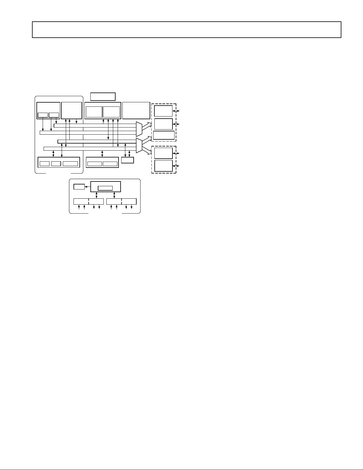
Figure 1. Functional Block Diagram
Figure 1 is an overall block diagram of the AD73422. The processor section contains three independent computational units:
the ALU, the multiplier/accumulator (MAC) and the shifter.
The computational units process 16-bit data directly and have
provisions to support multiprecision computations. The ALU
performs a standard set of arithmetic and logic operations; division primitives are also supported. The MAC performs singlecycle multiply, multiply/add and multiply/subtract operations
with 40 bits of accumulation. The shifter performs logical and
arithmetic shifts, normalization, denormalization and derive
exponent operations.
The internal result (R) bus connects the computational units so
that the output of any unit may be the input of any unit on the
next cycle.
A powerful program sequencer and two dedicated data address
generators ensure efficient delivery of operands to these computational units. The sequencer supports conditional jumps, subroutine calls and returns in a single cycle. With internal loop
counters and loop stacks, the AD73422 executes looped code
with zero overhead; no explicit jump instructions are required to
maintain loops.
Two data address generators (DAGs) provide addresses for
simultaneous dual operand fetches (from data memory and
program memory). Each DAG maintains and updates four
address pointers. Whenever the pointer is used to access data
(indirect addressing), it is post-modified by the value of one of
four possible modify registers. A length value may be associated
with each pointer to implement automatic modulo addressing
for circular buffers.
The two address buses (PMA and DMA) share a single external
address bus, allowing memory to be expanded off-chip, and the
two data buses (PMD and DMD) share a single external data
bus. Byte memory space and I/O memory space also share the
external buses.
An interface to low cost byte-wide memory is provided by the
Byte DMA port (BDMA port). The BDMA port is bidirectional
and can directly address up to four megabytes of external RAM
or ROM for off-chip storage of program overlays or data tables.
The AD73422 can respond to eleven interrupts. There can be
up to six external interrupts (one edge-sensitive, two levelsensitive and three configurable) and seven internal interrupts
generated by the timer, the serial ports (SPORTs), the Byte
DMA port and the power-down circuitry. There is also a master
RESET signal. The two serial ports provide a complete synchronous serial interface with optional companding in hardware and
a wide variety of framed or frameless data transmit and receive
modes of operation.
Each port can generate an internal programmable serial clock or
accept an external serial clock.
The AD73422 provides up to 13 general-purpose flag pins. The
data input and output pins on SPORT1 can be alternatively
configured as an input flag and an output flag. In addition, eight
flags are programmable as inputs or outputs and three flags are
always outputs.
A programmable interval timer generates periodic interrupts. A
16-bit count register (TCOUNT) is decremented every n processor cycle, where n is a scaling value stored in an 8-bit register
(TSCALE). When the value of the count register reaches zero,
an interrupt is generated and the count register is reloaded from
a 16-bit period register (TPERIOD).
Analog Front End
The AFE section is configured as a separate block that is normally connected to either SPORT0 or SPORT1 of the DSP
section. As it is not hardwired to either SPORT, the user has
total flexibility in how they wish to allocate system resources to
support the AFE. It is also possible to further expand the number of analog I/O channels connected to the SPORT by cascading other single or dual channel AFEs (AD73311 or AD73322)
external to the AD73422.
The AFE is configured as a cascade of two I/O channels (similar
to that of the discrete AD73322—refer to the AD73322 data sheet
for more details), with each channel having a separate 16-bit
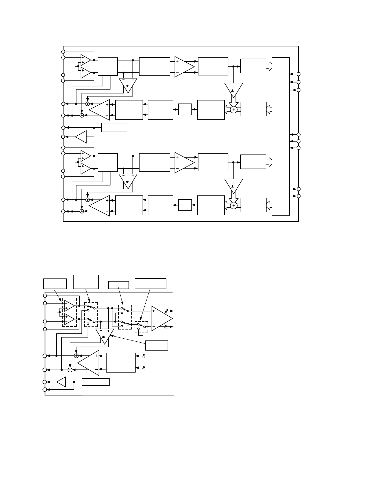
sigma-delta based ADC and DAC. Both channels share a common reference whose nominal value is 1.2 V. Figure 2 shows a
block diagram of the AFE section of the AD73422. It shows two
channels of ADC and DAC conversion, along with a common
reference. Communication to both channels is handled by the
SPORT2 block which interfaces to either SPORT0 or SPORT1 of
the DSP section.
Figure 3 shows the analog connectivity available on each channel of the AFE (Channel 1 is detailed here). Both channels
feature fully differential inputs and outputs. The input section
allows direct connection to the internal Programmable Gain
Amplifier at the input of the sigma-delta ADC section, or optional inverting amplifiers may be configured to provide some
fixed external gain or to interface to a transducer with relatively
high source impedance. The input section also features programmable differential channel inversion and configuration of
the differential input as two separate single-ended inputs. The
ADC features a second order sigma-delta modulator which
REV. 0
–9–
AD73422
VFBN1
VINN1
VINP1
VFBP1
V
REF
ANALOG
LOOP-
BACK
GAIN
1
INVERT
SINGLE-ENDED
ENABLE
0/38dB
PGA
ANALOG
SIGMA-DELTA
MODULATOR
GAIN
DECIMATOR
1
SDI
SDIFS
SCLK2
VOUTP1
VOUTN1
REFCAP
REFOUT
VFBN2
VINN2
VINP2
VFBP2
VOUTP2
VOUTN2
+6/–15dB
PGA
V
REF
+6/–15dB
PGA
REFERENCE
ANALOG
LOOP-
BACK
CONTINUOUS
TIME
LOW-PASS
FILTER
GAIN
1
CONTINUOUS
TIME
LOW-PASS
FILTER
SWITCHED
CAPACITOR
LOW-PASS
FILTER
INVERT
SINGLE-ENDED
ENABLE
SWITCHED
CAPACITOR
LOW-PASS
FILTER
AD73422
AFE SECTION
0/38dB
PGA
Figure 2. Functional Block Diagram of Analog Front End Section
samples at DMCLK/8. Its bitstream output is filtered and decimated by a Sinc-cubed decimator to provide a sample rate selectable from 64 kHz, 32 kHz, 16 kHz or 8 kHz (based on an
AMCLK of 16.384 MHz).
ANALOG
VFBN1
VINN1
VINP1
VFBP1
VOUTP1
VOUTN1
REFOUT
REFCAP
INVERTING
OP AMPS
V
REF
LOOP-BACK
SELECT
+6/–15dB
PGA
REFERENCE
GAIN
1
CONTINUOUS
LOW-PASS
INVERT
TIME
FILTER
SINGLE-ENDED
ENABLE
V
REF
ANALOG
GAIN TAP
AD73422
AFE SECTION
0/38dB
PGA
Figure 3. Analog Front End Configuration
The DAC channel features a Sinc-cubed interpolator which
increases the sample rate from the selected rate to the digital
sigma-delta modulator rate of DMCLK/8. The digital sigmadelta modulator’s output bitstream is fed to a single-bit DAC
whose output is reconstructed/filtered by two stages of low-pass
filtering (switched capacitor and continuous time) before being
applied to the differential output driver.
1-BIT
DAC
1-BIT
DAC
DIGITAL
SIGMADELTA
MODULATOR
ANALOG
SIGMA-DELTA
MODULATOR
DIGITAL
SIGMADELTA
MODULATOR
GAIN
DECIMATOR
1
INTER-
POLATOR
INTER-
POLATOR
SERIAL
I/O
PORT
ARESET
AMCLK
SE
SDO
SDOFS
Each channel also features two programmable gain elements,
Analog Gain Tap (AGT) and Digital Gain Tap (DGT), which,
when enabled, add a signed and scaled amount of the input
signal to the DAC’s output signal. This is of particular use in
line impedance balancing when interfacing the AFE to Subscriber Line Interface Circuits (SLICs).
FUNCTIONAL DESCRIPTION - AFE
Encoder Channels
Both encoder channels consist of a pair of inverting op amps
with feedback connections that can be bypassed if required, a
switched capacitor PGA and a sigma-delta analog-to-digital
converter (ADC). An on-board digital filter, which forms part
of the sigma-delta ADC, also performs critical system-level
filtering. Due to the high level of oversampling, the input antialias requirements are reduced such that a simple single-pole
RC stage is sufficient to give adequate attenuation in the band
of interest.
Programmable Gain Amplifier
Each encoder section’s analog front end comprises a switched
capacitor PGA which also forms part of the sigma-delta modulator. The SC sampling frequency is DMCLK/8. The PGA,
whose programmable gain settings are shown in Table I, may be
used to increase the signal level applied to the ADC from low
output sources such as microphones, and can be used to avoid
placing external amplifiers in the circuit. The input signal level
to the sigma-delta modulator should not exceed the maximum
input voltage permitted.
The PGA gain is set by bits IGS0, IGS1 and IGS2 (CRD:0–2)
in control register D.
–10–
REV. 0
AD73422
Table I. PGA Settings for the Encoder Channel
of these techniques, followed by the application of a digital
filter, sufficiently reduces the noise in band to ensure good
IGS2 IGS1 IGS0 Gain (dB)
000 0
001 6
010 12
011 18
100 20
101 26
110 32
111 38
dynamic performance from the part (Figure 4c).
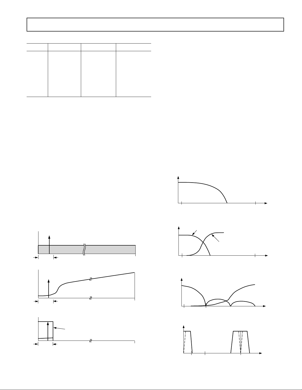
Figure 5 shows the various stages of filtering that are employed
in a typical AD73422 application. In Figure 5a we see the transfer function of the external analog antialias filter. Even though it
is a single RC pole, its cutoff frequency is sufficiently far away
from the initial sampling frequency (DMCLK/8) that it takes
care of any signals that could be aliased by the sampling frequency. This also shows the major difference between the initial
oversampling rate and the bandwidth of interest. In Figure 5b,
the signal and noise-shaping responses of the sigma-delta modu-
ADC
Both ADCs consist of an analog sigma-delta modulator and a
digital antialiasing decimation filter. The sigma-delta modulator noise-shapes the signal and produces 1-bit samples at a
DMCLK/8 rate. This bitstream, representing the analog input
signal, is input to the antialiasing decimation filter. The decimation filter reduces the sample rate and increases the resolution.
Analog Sigma-Delta Modulator
The AD73422’s input channels employ a sigma-delta conversion technique, which provides a high resolution 16-bit output
with system filtering being implemented on-chip.
Sigma-delta converters employ a technique known as oversampling where the sampling rate is many times the highest
lator are shown. The signal response provides further rejection
of any high frequency signals, while the noise-shaping will push
the inherent quantization noise to an out-of-band position. The
detail of Figure 5c shows the response of the digital decimation filter (Sinc-cubed response) with nulls every multiple of
DMCLK/256, which corresponds to the decimation filter update rate for a 64 kHz sampling. The nulls of the Sinc3 response
correspond with multiples of the chosen sampling frequency.
The final detail in Figure 5d shows the application of a final
antialias filter in the DSP engine. This has the advantage of
being implemented according to the user’s requirements and
available MIPS. The filtering in Figures 5a through 5c is implemented in the AD73422.
frequency of interest. In the case of the AD73422, the initial
sampling rate of the sigma-delta modulator is DMCLK/8. The
main effect of oversampling is that the quantization noise is
spread over a very wide bandwidth, up to F
/2 = DMCLK/16
S
(Figure 4a). This means that the noise in the band of interest is
much reduced. Another complementary feature of sigma-delta
converters is the use of a technique called noise-shaping. This
technique has the effect of pushing the noise from the band of
interest to an out-of-band position (Figure 4b). The combination
= DMCLK/8
FB = 4kHz
F
SINIT
a. Analog Antialias Filter Transfer Function
SIGNAL TRANSFER FUNCTION
REV. 0
BAND
OF
INTEREST
a.
NOISE-SHAPING
BAND
OF
INTEREST
b.
DIGITAL FILTER
BAND
OF
INTEREST
c.
Figure 4. Sigma-Delta Noise Reduction
FS/2
DMCLK/16
FS/2
DMCLK/16
FS/2
DMCLK/16
–11–
NOISE TRANSFER FUNCTION
= DMCLK/8
FB = 4kHz
F
SINIT
b. Analog Sigma-Delta Modulator Transfer Function
= DMCLK/256
FB = 4kHz
F
SINTER
c. Digital Decimator Transfer Function
FB = 4kHz
SFINAL
= 8kHz
F
SINTER
= DMCLK/256F
d. Final Filter LPF (HPF) Transfer Function
Figure 5. ADC Frequency Responses
 Loading...