BURIED ZENER REF
COMPARATOR
ANALOG
IN
DB9
HIGH
BYTE
10-BIT
CURRENT
OUTPUT
DAC
V+ V–
DIGITAL
COMMON
CONVERT
INT
CLOCK
10-BIT
SAR
DB8
DB7
DB6
DB5
DB4
DB3
DB2
DB1
DB0
HBE
LBE
MSB
LSB
LOW
BYTE
ANALOG
COMMON
BIPOLAR
OFFSET
CONTROL
DATA
READY
AD573
5k
a
10-Bit A/D Converter
AD573*
FEATURES
FUNCTIONAL BLOCK DIAGRAM
Complete 10-Bit A/D Converter with Reference, Clock
and Comparator
Full 8- or 16-Bit Microprocessor Bus Interface
Fast Successive Approximation Conversion—20 ms typ
No Missing Codes Over Temperature
Operates on +5 V and –12 V to –15 V Supplies
Low Cost Monolithic Construction
PRODUCT DESCRIPTION
The AD573 is a complete 10-bit successive approximation
analog-to-digital converter consisting of a DAC, voltage reference, clock, comparator, successive approximation register
(SAR) and three state output buffers—all fabricated on a single
chip. No external components are required to perform a full
accuracy 10-bit conversion in 20 µs.
The AD573 incorporates advanced integrated circuit design and
processing technologies. The successive approximation function
is implemented with I
2
L (integrated injection logic). Laser trimming of the high stability SiCr thin-film resistor ladder network
insures high accuracy, which is maintained with a temperature
compensated subsurface Zener reference.
Operating on supplies of +5 V and –12 V to –15 V, the AD573
will accept analog inputs of 0 V to +10 V or –5 V to +5 V. The
trailing edge of a positive pulse on the CONVERT line initiates
the 20 µs conversion cycle.
of the conversion.
HIGH BYTE ENABLE (HBE) and LOW
DATA READY indicates completion
BYTE ENABLE (LBE) control the 8-bit and 2-bit three state
output buffers.
PRODUCT HIGHLIGHTS
l. The AD573 is a complete 10-bit A/D converter. No external
components are required to perform a conversion.
2. The AD573 interfaces to many popular microprocessors
without external buffers or peripheral interface adapters. The
10 bits of output data can be read as a 10-bit word or as 8and 2-bit words.
3. The device offers true 10-bit accuracy and exhibits no missing codes over its entire operating temperature range.
4. The AD573 adapts to either unipolar (0 V to +10 V) or
bipolar (–5 V to +5 V) analog inputs by simply grounding or
opening a single pin.
5. Performance is guaranteed with +5 V and –12 V or –15 V
supplies.
6. The AD573 is available in a version compliant with MIL-STD-
883. Refer to the Analog Devices Military Products Databook or current /883B data sheet for detailed specifications.
The AD573 is available in two versions for the 0°C to +70°C
temperature range, the AD573J and AD573K. The AD573S
guarantees ±1 LSB relative accuracy and no missing codes from
–55°C to +125°C.
Three package configurations are offered. All versions are offered
in a 20-pin hermetically sealed ceramic DIP. The AD573J and
AD573K are also available in a 20-pin plastic DIP or 20-pin
leaded chip carrier.
*Protected by U.S. Patent Nos. 3,940,760; 4,213,806; 4,136,349; 4,400,689;
and 4,400,690.
REV. A
Information furnished by Analog Devices is believed to be accurate and
reliable. However, no responsibility is assumed by Analog Devices for its
use, nor for any infringements of patents or other rights of third parties
which may result from its use. No license is granted by implication or
otherwise under any patent or patent rights of Analog Devices.
One Technology Way, P.O. Box 9106, Norwood, MA 02062-9106, U.S.A.
Tel: 617/329-4700 Fax: 617/326-8703

(@ TA = +258C, V+ = +5 V, V– = –12 V or –15 V, all voltages measured with respect
AD573–SPECIFICATIONS
Model Min Typ Max Min Typ Max Min Typ Max Units
RESOLUTION 10 10 10 Bits
RELATIVE ACCURACY
TA = T
MIN
to T
FULL-SCALE CALIBRATION
UNIPOLAR OFFSET 61 61/2 61 LSB
BIPOLAR OFFSET 61 61/2 61 LSB
DIFFERENTIAL NONLINEARITY
TA = T
MIN
to T
TEMPERATURE RANGE 0 +70 0 +70 –55 +125 °C
TEMPERATURE COEFFICIENTS
Unipolar Offset 62 61 62 LSB
Bipolar Offset 62 61 62 LSB
Full-Scale Calibration
POWER SUPPLY REJECTION
Positive Supply
+4.5 V ≤ V + ≤ +5.5 V 62 61 62 LSB
Negative Supply
–15.75 V ≤ V – ≤ –14.25 V 62 61 62 LSB
–12.6 V ≤ V – ≤ –11.4 V 62 61 62 LSB
ANALOG INPUT IMPEDANCE 3.0 5.0 7.0 3.0 5.0 7.0 3.0 5.0 7.0 kΩ
ANALOG INPUT RANGES
Unipolar 0 +10 0 +10 0 +10 V
Bipolar –5 +5 –5 +5 –5 +5 V
OUTPUT CODING
Unipolar Positive True Binary Positive True Binary Positive True Binary
Bipolar Positive True Offset Binary Positive True Offset Binary Positive True Offset Binary
LOGIC OUTPUT
Output Sink Current
= 0.4 V max, T
(V
OUT
Output Source Current
(V
= 2.4 V min, T
OUT
Output Leakage 640 640 640 µA
LOGIC INPUTS
Input Current 6100 6100 6100 µA
Logic “1” 2.0 2.0 2.0 V
Logic “0” 0.8 0.8 0.8 V
CONVERSION TIME
TA = T
MIN
to T
POWER SUPPLY
V+ +4.5 5.0 +7.0 +4.5 +5.0 +7.0 +4.5 +5.0 +7.0 V
V– –11.4 –15 –16.5 +11.4 –15 –16.5 –11.4 –15 –16.5 V
OPERATING CURRENT
V+ 15 20 15 20 15 20 mA
V– 9 15 9 15 9 15 mA
NOTES
1
Relative accuracy is defined as the deviation of the code transition points from the ideal transfer point on a straight line from the zero to the full scale of the device.
2
Full-scale calibration is guaranteed trimmable to zero with an external 50 Ω potentiometer in place of the 15 Ω fixed resistor. Full scale is defined as 10 volts minus
1 LSB, or 9.990 volts.
3
Defined as the resolution for which no missing codes will occur.
4
Change from +25°C value from +25°C to T
5
The data output lines have active pull-ups to source 0.5 mA. The DATA READY line is open collector with a nominal 6 kΩ internal pull-up resistor.
Specifications subject to change without notice.
Specifications shown in boldface are tested on all production units at final electrical test. Results from those tests are used to calculate outgoing quality levels. All min
and max specifications are guaranteed, although only those shown in boldface are tested on all production units.
MAX
MAX
MAX
1
2
3
4
2
to T
5
MIN
MIN
to T
) 3.2 3.2 3.2 mA
MAX
) 0.5 0.5 0.5 mA
MAX
or T
MIN
to digital common, unless otherwise noted.)
AD573J AD573K AD573S
61 61/2 61 LSB
61 61/2 61 LSB
±2 ±2 62 LSB
10 10 10 Bits
91010Bits
64 62 65 LSB
10 20 30 10 20 30 10 20 30 µs
.
MAX
–2–
REV. A

ABSOLUTE MAXIMUM RATINGS
BURIED ZENER REF
COMPARATOR
ANALOG
IN
DB9
HIGH
BYTE
10-BIT
CURRENT
OUTPUT
DAC
V+ V–
DIGITAL
COMMON
CONVERT
INT
CLOCK
10-BIT
SAR
DB8
DB7
DB6
DB5
DB4
DB3
DB2
DB1
DB0
HBE
LBE
MSB
LSB
LOW
BYTE
ANALOG
COMMON
BIPOLAR
OFFSET
CONTROL
DATA
READY
AD573
5k
V+ to Digital Common . . . . . . . . . . . . . . . . . . . . . 0 V to +7 V
V– to Digital Common . . . . . . . . . . . . . . . . . . . 0 V to –16.5 V
Analog Common to Digital Common . . . . . . . . . . . . . . . ±1 V
Analog Input to Analog Common . . . . . . . . . . . . . . . . . ±15 V
Control Inputs . . . . . . . . . . . . . . . . . . . . . . . . . . . . . . 0 V to V+
Digital Outputs (High Impedance State) . . . . . . . . . .0 V to V+
Power Dissipation . . . . . . . . . . . . . . . . . . . . . . . . . . . .800 mW
AD573
ORDERING GUIDE
Model Package Option
2
AD573JN 20-Pin Plastic DIP (N-20) 0°C to +70°C ±1 LSB max
AD573KN 20-Pin Plastic DIP (N-20) 0°C to +70°C ±1/2 LSB max
AD573JP 20-Pin Leaded Chip Carrier (P-20A) 0°C to +70°C ±1 LSB max
AD573KP 20-Pin Leaded Chip Carrier (P-20A) 0°C to +70°C ±1/2 LSB max
AD573JD 20-Pin Ceramic DIP (D-20) 0°C to +70°C ± 1 LSB max
AD573KD 20-Pin Ceramic DIP (D-20) 0°C to +70°C ±1/2 LSB max
AD573 SD 20-Pin Ceramic DIP (D-20) –55°C to +125°C ±1 LSB max
NOTES
1
For details on grade and package offerings screened in accordance with MIL-STD-883, refer to Analog Devices Military
Products Databook.
2
D = Ceramic DIP; N = Plastic DIP; P = Plastic Leaded Chip Carrier.
FUNCTIONAL DESCRIPTION
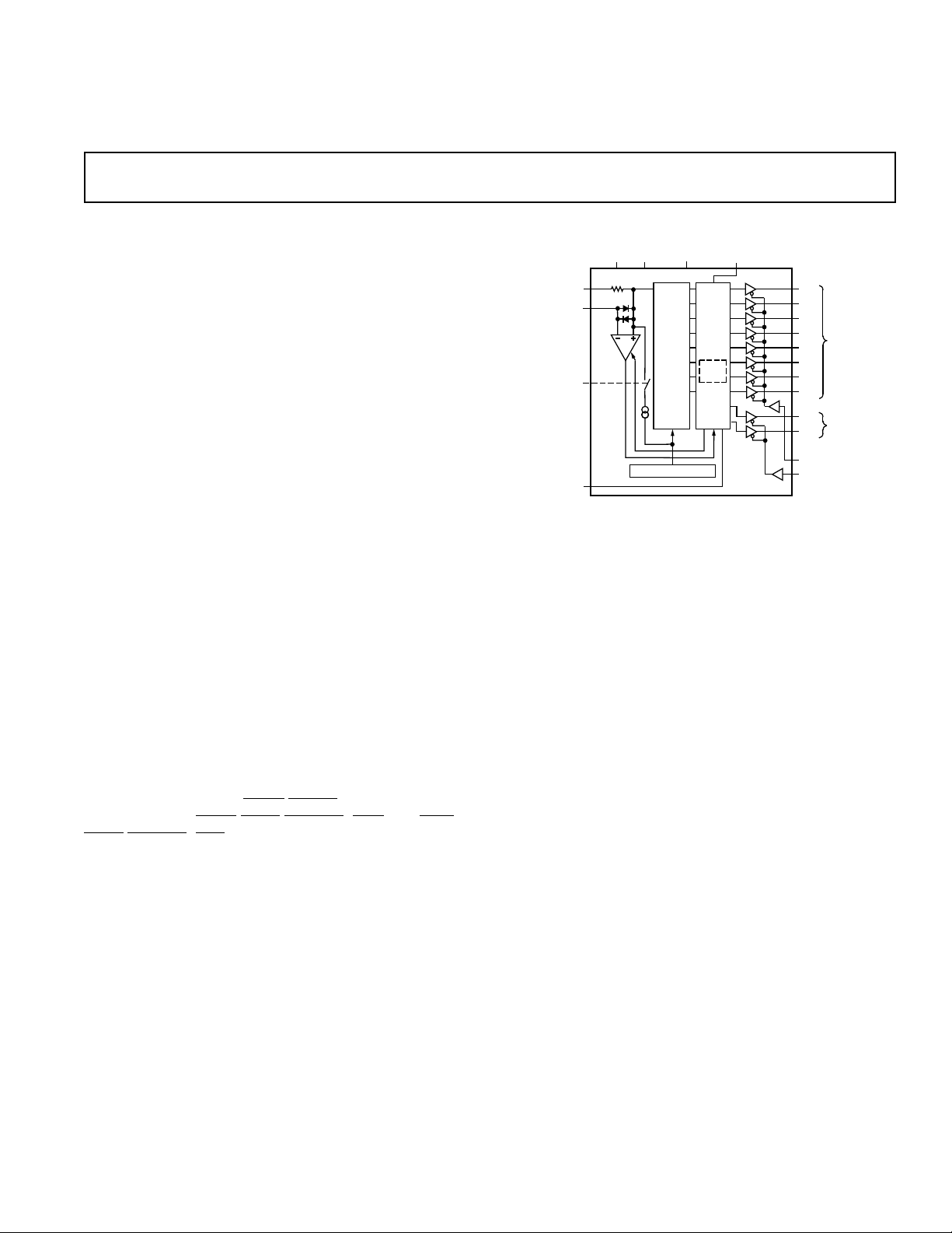
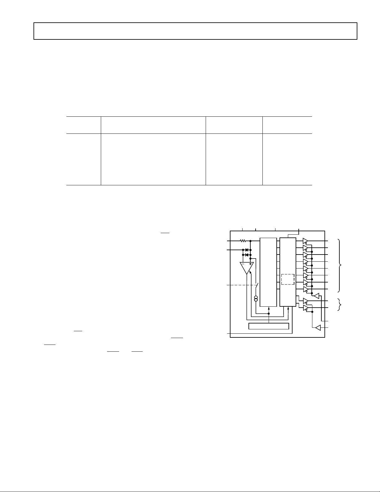
A block diagram of the AD573 is shown in Figure 1. The positive CONVERT pulse must be at least 500 ns wide.
DR goes
high within 1.5 µs after the leading edge of the convert pulse
indicating that the internal logic has been reset. The negative
edge of the CONVERT pulse initiates the conversion. The internal 10-bit current output DAC is sequenced by the integrated
injection logic (I
2
L) successive approximation register (SAR)
from its most significant bit to least significant bit to provide an
output current which accurately balances the input signal current through the 5 kΩ resistor. The comparator determines
whether the addition of each successively weighted bit current
causes the DAC current sum to be greater or less than the input
current; if the sum is more, the bit is turned off. After testing all
bits, the SAR contains a 10-bit binary code which accurately
represents the input signal to within 1/2 LSB (0.05% of full scale).
The SAR drives
DR low to indicate that the conversion is complete and that the data is available to the output buffers.
and
LBE can then be activated to enable the upper 8-bit and
lower 2-bit buffers as desired.
HBE and LBE should be brought
high prior to the next conversion to place the output buffers in
the high impedance state.
The temperature compensated buried Zener reference provides
the primary voltage reference to the DAC and ensures excellent
stability with both time and temperature. The bipolar offset input controls a switch which allows the positive bipolar offset
current (exactly equal to the value of the MSB less 1/2 LSB) to
be injected into the summing (+) node of the comparator to
offset the DAC output. Thus the nominal 0 V to +10 V unipolar
input range becomes a –5 V to +5 V range. The 5 kΩ thin-film
input resistor is trimmed so that with a full-scale input signal, an
input current will be generated which exactly matches the DAC
output with all bits on.
REV. A
1
Temperature Relative
Range Accuracy
HBE
Figure 1. Functional Block Diagram
UNIPOLAR CONNECTION
The AD573 contains all the active components required to perform a complete A/D conversion. Thus, for many applications,
all that is necessary is connection of the power supplies (+5 V
and –12 V to –15 V), the analog input and the convert pulse.
However, there are some features and special connections which
should be considered for achieving optimum performance. The
functional pinout is shown in Figure 2.
The standard unipolar 0 V to +10 V range is obtained by shorting the bipolar offset control pin (Pin 16) to digital common
(Pin 17).
–3–
 Loading...