

BURIED ZENER REF
COMPARATOR
ANALOG
IN
DB9
HIGH
BYTE
10-BIT
CURRENT
OUTPUT
DAC
V+ V–
DIGITAL
COMMON
CONVERT
INT
CLOCK
10-BIT
SAR
DB8
DB7
DB6
DB5
DB4
DB3
DB2
DB1
DB0
HBE
LBE
MSB
LSB
LOW
BYTE
ANALOG
COMMON
BIPOLAR
OFFSET
CONTROL
DATA
READY
AD573
5k
a
REV. B
Tel: 781.329.4700
Fax: 781.461.3113
10-Bit A/D Converter
AD573
PRODUCT DESCRIPTION
The AD573 is a complete 10-bit successive approximation
analog-to-digital converter consisting of a DAC, voltage reference, clock, comparator, successive approximation register
(SAR) and three state output buffers—all fabricated on a single
chip. No external components are required to perform a full
accuracy 10-bit conversion in 20 µs.
The AD573 incorporates advanced integrated circuit design and
processing technologies. The successive approximation function
is implemented with I
ming of the high stability SiCr thin-film resistor ladder network
insures high accuracy, which is maintained with a temperature
compensated subsurface Zener reference.
Operating on supplies of +5 V and –12 V to –15 V, the AD573
will accept analog inputs of 0 V to +10 V or –5 V to +5 V. The
trailing edge of a positive pulse on the CONVERT line initiates
the 20 µs conversion cycle.
of the conversion.
BYTE ENABLE (LBE) control the 8-bit and 2-bit three state
output buffers.
The AD573 is available in two versions for the 0°C to +70°C
temperature range, the AD573J and AD573K. The AD573S
guarantees ±1 LSB relative accuracy and no missing codes from
–55°C to +125°C.
Three package configurations are offered. All versions are offered
in a 20-pin hermetically sealed ceramic DIP. The AD573J and
AD573K are also available in a 20-pin plastic DIP or 20-pin
leaded chip carrier.
Information furnished by Analog Devices is believed to be accurate and
reliable. However, no responsibility is assumed by Analog Devices for its
use, nor for any infringements of patents or other rights of third parties
which may result from its use. No license is granted by implication or
otherwise under any patent or patent rights of Analog Devices.
FEATURES
Complete 10-Bit A/D Converter with Reference, Clock
and Comparator
Full 8- or 16-Bit Microprocessor Bus Interface
Fast Successive Approximation Conversion—20 ms typ
No Missing Codes Over Temperature
Operates on +5 V and –12 V to –15 V Supplies
Low Cost Monolithic Construction
2
L (integrated injection logic). Laser trim-
DATA READY indicates completion
HIGH BYTE ENABLE (HBE) and LOW
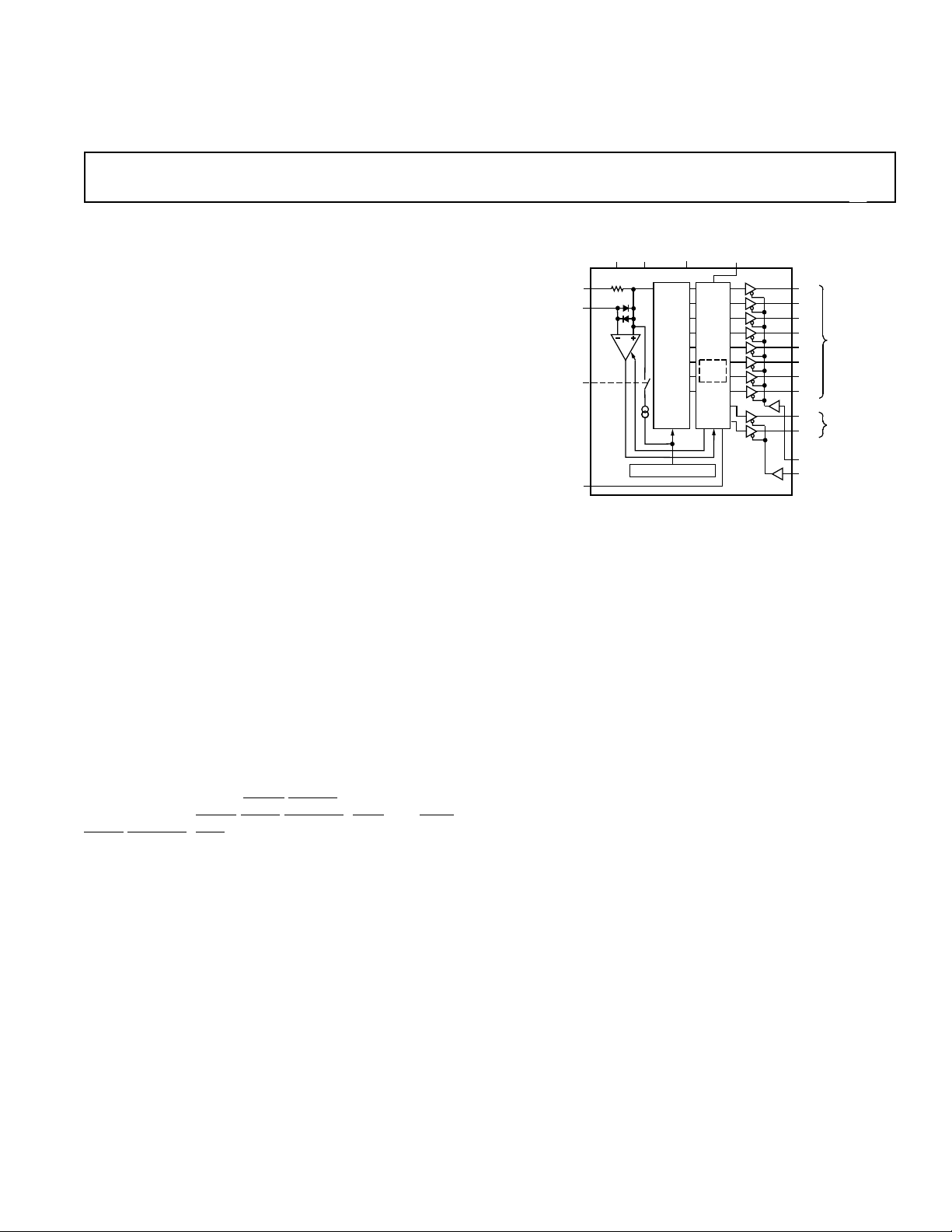
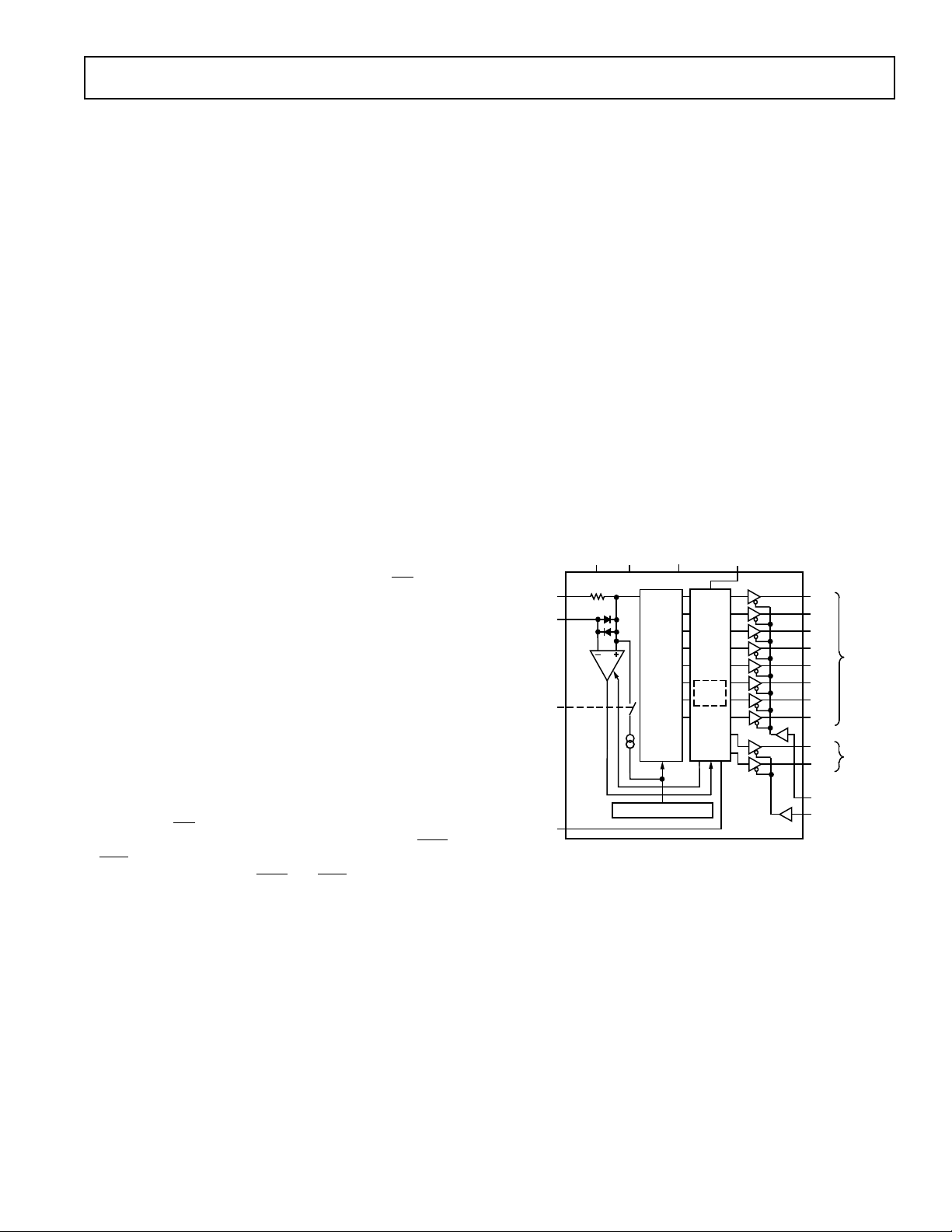
FUNCTIONAL BLOCK DIAGRAM
PRODUCT HIGHLIGHTS
l. The AD573 is a complete 10-bit A/D converter. No external
components are required to perform a conversion.
2. The AD573 interfaces to many popular microprocessors
without external buffers or peripheral interface adapters. The
10 bits of output data can be read as a 10-bit word or as 8and 2-bit words.
3. The device offers true 10-bit accuracy and exhibits no missing codes over its entire operating temperature range.
4. The AD573 adapts to either unipolar (0 V to +10 V) or
bipolar (–5 V to +5 V) analog inputs by simply grounding or
opening a single pin.
5. Performance is guaranteed with +5 V and –12 V or –15 V
supplies.
6. The AD573 is available in a version compliant with MIL-STD-
883. Refer to the Analog Devices Military Products Databook or current /883B data sheet for detailed specifications.
One Technology Way, P.O. Box 9106, Norwood, MA 02062-9106, U.S.A.

(@ TA = +258C, V+ = +5 V, V– = –12 V or –15 V, all voltages measured with respect
REV. B
8
AD573–SPECIFICATIONS
Model Min Typ Max Min Typ Max Min Typ Max Units
RESOLUTION 10 10 10 Bits
RELATIVE ACCURACY
TA = T
MIN
to T
FULL-SCALE CALIBRATION
UNIPOLAR OFFSET 61 61/2 61 LSB
BIPOLAR OFFSET 61 61/2 61 LSB
DIFFERENTIAL NONLINEARITY
TA = T
MIN
to T
TEMPERATURE RANGE 0 +70 0 +70 –55 +125 °C
TEMPERATURE COEFFICIENTS
Unipolar Offset 62 61 62 LSB
Bipolar Offset 62 61 62 LSB
Full-Scale Calibration
POWER SUPPLY REJECTION
Positive Supply
+4.5 V ≤ V + ≤ +5.5 V 62 61 62 LSB
Negative Supply
–15.75 V ≤ V – ≤ –14.25 V 62 61 62 LSB
–12.6 V ≤ V – ≤ –11.4 V 62 61 62 LSB
ANALOG INPUT IMPEDANCE 3.0 5.0 7.0 3.0 5.0 7.0 3.0 5.0 7.0 kΩ
ANALOG INPUT RANGES
Unipolar 0 +10 0 +10 0 +10 V
Bipolar –5 +5 –5 +5 –5 +5 V
OUTPUT CODING
Unipolar Positive True Binary Positive True Binary Positive True Binary
Bipolar Positive True Offset Binary Positive True Offset Binary Positive True Offset Binary
LOGIC OUTPUT
Output Sink Current
= 0.4 V max, T
(V
OUT
Output Source Current
(V
= 2.4 V min, T
OUT
Output Leakage 640 640 640 µA
LOGIC INPUTS
Input Current 6100 6100 6100 µA
Logic “1” 2.0 2.0 2.0 V
Logic “0” 0.8 0.8 0.8 V
CONVERSION TIME
TA = T
MIN
to T
POWER SUPPLY
V+ +4.5 5.0 +7.0 +4.5 +5.0 +7.0 +4.5 +5.0 +7.0 V
V– –11.4 –15 –16.5 +11.4 –15 –16.5 –11.4 –15 –16.5 V
OPERATING CURRENT
V+ 15 20 15 20 15 20 mA
V– 9 15 9 15 9 15 mA
NOTES
1
Relative accuracy is defined as the deviation of the code transition points from the ideal transfer point on a straight line from the zero to the full scale of the device.
2
Full-scale calibration is guaranteed trimmable to zero with an external 50 Ω potentiometer in place of the 15 Ω fixed resistor. Full scale is defined as 10 volts minus
1 LSB, or 9.990 volts.
3
Defined as the resolution for which no missing codes will occur.
4
Change from +25°C value from +25°C to T
5
The data output lines have active pull-ups to source 0.5 mA. The DATA READY line is open collector with a nominal 6 kΩ internal pull-up resistor.
Specifications subject to change without notice.
Specifications shown in boldface are tested on all production units at final electrical test. Results from those tests are used to calculate outgoing quality levels. All min
and max specifications are guaranteed, although only those shown in boldface are tested on all production units.
MAX
MAX
MAX
1
2
3
4
2
to T
5
MIN
MIN
to T
) 3.2 3.2 3.2 mA
MAX
) 0.5 0.5 0.5 mA
MAX
or T
MIN
to digital common, unless otherwise noted.)
AD573J AD573K AD573S
61 61/2 61 LSB
61 61/2 61 LSB
±2 ±2 62 LSB
10 10 10 Bits
91010Bits
64 62 6 LSB
10 20 30 10 20 30 10 20 30 µs
.
MAX
–2–
ABSOLUTE MAXIMUM RATINGS
BURIED ZENER REF
COMPARATOR
ANALOG
IN
DB9
HIGH
BYTE
10-BIT
CURRENT
OUTPUT
DAC
V+ V–
DIGITAL
COMMON
CONVERT
INT
CLOCK
10-BIT
SAR
DB8
DB7
DB6
DB5
DB4
DB3
DB2
DB1
DB0
HBE
LBE
MSB
LSB
LOW
BYTE
ANALOG
COMMON
BIPOLAR
OFFSET
CONTROL
DATA
READY
AD573
5k
REV. B
V+ to Digital Common . . . . . . . . . . . . . . . . . . . . . 0 V to +7 V
V– to Digital Common . . . . . . . . . . . . . . . . . . . 0 V to –16.5 V
Analog Common to Digital Common . . . . . . . . . . . . . . . ±1 V
Analog Input to Analog Common . . . . . . . . . . . . . . . . . ±15 V
Control Inputs . . . . . . . . . . . . . . . . . . . . . . . . . . . . . . 0 V to V+
Digital Outputs (High Impedance State) . . . . . . . . . .0 V to V+
Power Dissipation . . . . . . . . . . . . . . . . . . . . . . . . . . . .800 mW
AD573
FUNCTIONAL DESCRIPTION
A block diagram of the AD573 is shown in Figure 1. The positive CONVERT pulse must be at least 500 ns wide.
DR goes
high within 1.5 µs after the leading edge of the convert pulse
indicating that the internal logic has been reset. The negative
edge of the CONVERT pulse initiates the conversion. The internal 10-bit current output DAC is sequenced by the integrated
injection logic (I
2
L) successive approximation register (SAR)
from its most significant bit to least significant bit to provide an
output current which accurately balances the input signal current through the 5 kΩ resistor. The comparator determines
whether the addition of each successively weighted bit current
causes the DAC current sum to be greater or less than the input
current; if the sum is more, the bit is turned off. After testing all
bits, the SAR contains a 10-bit binary code which accurately
represents the input signal to within 1/2 LSB (0.05% of full scale).
The SAR drives
plete and that the data is available to the output buffers.
and
LBE can then be activated to enable the upper 8-bit and
lower 2-bit buffers as desired.
DR low to indicate that the conversion is com-
HBE
HBE and LBE should be brought
high prior to the next conversion to place the output buffers in
the high impedance state.
The temperature compensated buried Zener reference provides
the primary voltage reference to the DAC and ensures excellent
stability with both time and temperature. The bipolar offset input controls a switch which allows the positive bipolar offset
current (exactly equal to the value of the MSB less 1/2 LSB) to
be injected into the summing (+) node of the comparator to
offset the DAC output. Thus the nominal 0 V to +10 V unipolar
input range becomes a –5 V to +5 V range. The 5 kΩ thin-film
input resistor is trimmed so that with a full-scale input signal, an
input current will be generated which exactly matches the DAC
output with all bits on.
Figure 1. Functional Block Diagram
UNIPOLAR CONNECTION
The AD573 contains all the active components required to perform a complete A/D conversion. Thus, for many applications,
all that is necessary is connection of the power supplies (+5 V
and –12 V to –15 V), the analog input and the convert pulse.
However, there are some features and special connections which
should be considered for achieving optimum performance. The
functional pinout is shown in Figure 2.
The standard unipolar 0 V to +10 V range is obtained by shorting the bipolar offset control pin (Pin 16) to digital common
(Pin 17).
–3–

AD573
REV. B
LSB DB0
DB1
DB2
DB3
DB4
DB5
DB6
DB7
DB8
MSB DB9
1
PIN 1
IDENTIFIER
2
3
4
5
AD573
TOP VIEW
6
(Not to Scale)
7
8
9
10
20
HBE
LBE
19
DR
18
DIG COM
17
BIP OFF
16
ANALOG COM
15
ANALOG IN
14
13
V–
CONVERT
12
V+
11
Figure 2. AD573 Pin Connections
Full-Scale Calibration
The 5 kΩ thin-film input resistor is laser trimmed to produce a
current which matches the full-scale current of the internal
DAC—plus about 0.3%—when an analog input voltage of 9.990
volts (10 volts – 1 LSB) is applied at the input. The input resistor is trimmed in this way so that if a fine trimming potentiometer is inserted in series with the input signal, the input current
at the full-scale input voltage can be trimmed down to match
the DAC full-scale current as precisely as desired. However, for
many applications the nominal 9.99 volt full scale can be
achieved to sufficient accuracy by simply inserting a 15 Ω resistor in series with the analog input to Pin 14. Typical full-scale
calibration error will then be within ± 2 LSB or ±0.2%. If more
precise calibration is desired, a 50 Ω trimmer should be used
instead. Set the analog input at 9.990 volts, and set the trimmer
so that the output code is just at the transition between
11111111 10 and 11111111 11. Each LSB will then have a
weight of 9.766 mV. If a nominal full scale of 10.24 volts is desired (which makes the LSB have a weight of exactly 10.00 mV),
a 100 Ω resistor and a 100 Ω trimmer (or a 200 Ω trimmer with
good resolution) should be used. Of course, larger full-scale
ranges can be arranged by using a larger input resistor, but linearity and full-scale temperature coefficient may be compromised if the external resistor becomes a sizeable percentage of
5 kΩ. Figure 3 illustrates the connections required for full-scale
calibration.
Figure 3. Standard AD573 Connections
Unipolar Offset Calibration
Since the Unipolar Offset is less than ± 1 LSB for all versions of
the AD573, most applications will not require trimming. Figure
4 illustrates two trimming methods which can be used if greater
accuracy is necessary.
Figure 4a shows how the converter zero may be offset by up to
±3 bits to correct the device initial offset and/or input signal
offsets. As shown, the circuit gives approximately symmetrical
adjustment in unipolar mode.
Figure 4a. Figure 4b.
Figure 4. Offset Trims
Figure 5 shows the nominal transfer curve near zero for an
AD573 in unipolar mode. The code transitions are at the edges
of the nominal bit weights. In some applications it will be preferable to offset the code transitions so that they fall between the
nominal bit weights, as shown in the offset characteristics.
Figure 5. AD573 Transfer Curve—Unipolar Operation
(Approximate Bit Weights Shown for Illustration, Nominal
Bit Weights ~ 9.766 mV)
This offset can easily be accomplished as shown in Figure 4b. At
balance (after a conversion) approximately 2 mA flows into the
Analog Common terminal. A 2.7 Ω resistor in series with this
terminal will result in approximately the desired 1/2 bit offset of
the transfer characteristics. The nominal 2 mA Analog Common
current is not closely controlled in manufacture. If high accuracy is required, a 5 Ω potentiometer (connected as a rheostat)
can be used as R1. Additional negative offset range may be obtained by using larger values of R1. Of course, if the zero transition point is changed, the full-scale transition point will also
move. Thus, if an offset of 1/2 LSB is introduced, full-scale
trimming as described on the previous page should be done with
an analog input of 9.985 volts.
NOTE: During a conversion, transient currents from the Analog
Common terminal will disturb the offset voltage. Capacitive
decoupling should not be used around the offset network. These
transients will settle appropriately during a conversion. Capacitive decoupling will “pump up” and fail to settle resulting in
conversion errors. Power supply decoupling, which returns to
analog signal common, should go to the signal input side of the
resistive offset network.
–4–

AD573
REV. B
BIPOLAR CONNECTION
To obtain the bipolar –5 V to +5 V range with an offset binary
output code, the bipolar offset control pin is left open.
A –5.000 volt signal will give a 10-bit code of 00000000 00; an
input of 0.000 volts results in an output code of 10000000 00
and +4.99 volts at the input yields the 11111111 11 code. The
nominal transfer curve is shown in Figure 6.
Figure 6. AD573 Transfer Curve— Bipolar Operation
Note that in the bipolar mode, the code transitions are offset
1/2 LSB such that an input voltage of 0 volts ± 5 mV yields the
code representing zero (10000000 00). Each output code is then
centered on its nominal input voltage.
Full-Scale Calibration
Full-Scale Calibration is accomplished in the same manner as in
unipolar operation except the full scale input voltage is +4.985
volts.
Negative Full-Scale Calibration
The circuit in Figure 4a can also be used in bipolar operation to
offset the input voltage (nominally –5 V) which results in the
00000000 00 code. R2 should be omitted to obtain a symmetrical range.
The bipolar offset control input is not directly TTL compatible
but a TTL interface for logic control can be constructed as
shown in Figure 7.
SAMPLE-HOLD AMPLIFIER CONNECTION TO THE
AD573
Many situations in high speed acquisition systems or digitizing
rapidly changing signals require a sample-hold amplifier (SHA)
in front of the A/D converter. The SHA can acquire and hold a
signal faster than the converter can perform a conversion. A
SHA can also be used to accurately define the exact point in
time at which the signal is sampled. For the AD573, a SHA can
also serve as a high input impedance buffer.
Figure 8 shows the AD573 connected to the AD582 monolithic
SHA for high speed signal acquisition. In this configuration, the
AD582 will acquire a 10 volt signal in less than 10 µs with a
droop rate less than 100 µV/ms.
Figure 8. Sample-Hold Interface to the AD573
DR goes high after the conversion is initiated to indicate that
reset of the SAR is complete. In Figure 8 it is also used to put
the AD582 into the hold mode while the AD573 begins its conversion cycle. (The AD582 settles to final value well in advance
of the first comparator decision inside the AD573).
DR goes low when the conversion is complete placing the
AD582 back in the sample mode. Configured as shown in Figure 8, the next conversion can be initiated after a 10 µs delay to
allow for signal acquisition by the AD582.
Observe carefully the ground, supply, and bypass capacitor connections between the two devices. This will minimize ground
noise and interference during the conversion cycle.
Figure 7. Bipolar Offset Controlled by Logic Gate
Gate Output = 1 Unipolar 0–10 V Input Range
Gate Output = 0 Bipolar ±5 V Input Range
GROUNDING CONSIDERATIONS
The AD573 provides separate Analog and Digital Common
connections. The circuit will operate properly with as much as
±200 mV of common-mode voltage between the two commons.
This permits more flexible control of system common bussing
and digital and analog returns.
In normal operation, the Analog Common terminal may generate transient currents of up to 2 mA during a conversion. In addition a static current of about 2 mA will flow into Analog
Common in the unipolar mode after a conversion is complete.
The Analog Common current will be modulated by the variations in input signal.
The absolute maximum voltage rating between the two commons is ±1 volt. It is recommended that a parallel pair of
back-to-back protection diodes be connected between the commons if they are not connected locally.
–5–

AD573
REV. B
CONTROL AND TIMING OF THE AD573
The operation of the AD573 is controlled by three inputs:
CONVERT, HBE and LBE.
Starting a Conversion
The conversion cycle is initiated by a positive going CONVERT
pulse at least 500 ns wide. The rising edge of this pulse resets
the internal logic, clears the result of the previous conversion,
and sets
conversion cycle. When conversion is completed
low. During the conversion cycle,
high. If
DR high. The falling edge of CONVERT begins the
DR returns
HBE and LBE should be held
HBE or LBE goes low during a conversion, the data
output buffers will be enabled and intermediate conversion results will be present on the data output pins. This may cause
bus conflicts if other devices in a system are trying to use the bus.
V
+ V
IH
CONVERT
DR
IL
2
t
CS
t
DSC
VOH + V
2
t
C
OL
Figure 9. Convert Timing
Reading the Data
The three-state data output buffers are enabled by HBE and
LBE. Access time of these buffers is typically 150 ns (250 maxi-
mum). The data outputs remain valid until 50 ns after the enable signal returns high, and are completely into the high
impedance state 100 ns later.
pulse, and gating it with RD to enable the output buffers. The
use of a memory address and memory WR and RD signals denotes “memory-mapped” I/O interfacing, while the use of a
separate I/O address space denotes “isolated I/O” interfacing. In
8-bit bus systems, the 10-bit AD573 will occupy two locations
when data is to be read; therefore, two (usually consecutive) addresses must be decoded. One of the addresses can also be used
as the address which produces the CONVERT signal during
WR operations.
Figure 11 shows a generalized diagram of the control logic for
an AD573 interfaced to an 8-bit data bus, where two addresses
(ADC ADDR and ADC ADDR + 1) have been decoded. ADC
ADDR starts the converter when written to (the actual data being written to the converter does not matter) and contains the
high byte data during read operations. ADC ADDR + 1 performs no function during write operations, but contains the low
byte data during read operations.
VIH + V
LBE OR HBE
DB0–DB7
OR
DB8–DB9
IL
2
HIGH
IMPEDANCE
t
DD
V
OH
V
OL
DATA
VALID
t
HD
t
HL
HIGH
IMPEDANCE
Figure 10. Read Timing
TIMING SPECIFICATIONS (All grades, TA = T
MIN–TMAX
)
Parameter Symbol Min Typ Max Units
CONVERT Pulse Width t
DR Delay from CONVERT t
Conversion Time t
Data Access Time t
Data Valid after
HBE/LBE
High t
Output Float Delay t
CS
DSC
C
DD
HD
HL
500 – – ns
– 1 1.5 µs
10 20 30 µs
0 150 250 ns
50 – – ns
– 100 200 ns
MICROPROCESSOR INTERFACE CONSIDERATIONS—
GENERAL
When an analog-to-digital converter like the AD573 is interfaced to a microprocessor, several details of the interface must
be considered. First, a signal to start the converter must be generated; then an appropriate delay period must be allowed to pass
before valid conversion data may be read. In most applications,
the AD573 can interface to a microprocessor system with little
or no external logic.
The most popular control signal configuration consists of decoding the address assigned to the AD573, then gating this signal with the system’s WR signal to generate the CONVERT
–6–
Figure 11. General AD573 Interface to 8-Bit Microprocessor
In systems where this read-write interface is used, at least 30
microseconds (the maximum conversion time) must be allowed
to pass between starting a conversion and reading the results.
This delay or “timeout” period can be implemented in a short
software routine such as a countdown loop, enough dummy instructions to consume 30 microseconds, or enough actual useful
instructions to consume the required time. In tightly-timed systems, the
DR line may be read through an external three-state
buffer to determine precisely when a conversion is complete.
Higher speed systems may choose to use
DR to signal an inter-
rupt to the processor at the end of a conversion.
Figure 12. Typical AD573 Interface Timing Diagram

AD573
REV. B
CONVERT Pulse Generation
The AD573 is tested with a CONVERT pulse width of 500 ns
and will typically operate with a pulse as short as 300 ns.
However, some microprocessors produce active WR pulses
which are shorter than this. Either of the circuits shown in Figure 13 can be used to generate an adequate CONVERT pulse
for the AD573.
In both circuits, the short low going WR pulse sets the
CONVERT line high through a flip-flop. The rising edge of
DR (which signifies that the internal logic has been reset) resets
the flip-flop and brings CONVERT low, which starts the
conversion.
Note that t
conversion contains a Logic 1 on the LSB. This means that the
actual CONVERT pulse generated by the circuits in Figure 13
will vary slightly in width.
Figure 13a. Using 74LS00 Figure 13b. Using 1/2 74LS74
Output Data Format
The AD573 output data is presented in a left justified format.
The 8 MSBs (DB9–DB2, Pins 10 through 3) are enabled by
HBE (Pin 20) and the 2 LSBs (DB1, DB0—Pins 2 and 1) are
enabled by
system buses by overlapping the 2 MSBs and the 2 LSBs. The
organization of the data is shown in Figure 14.
When the least significant bits are read (
six remaining bits of the byte will contain meaningless data.
These unwanted bits can be masked by logically ANDing the
byte with 11000000 (C0 hex), which forces the 6 lower bits to
Logic 0 while preserving the two most significant bits of the byte.
Note that it is not possible to reconfigure the AD573 for right
justified data.
is slightly longer when the result of the previous
DSC
LBE (Pin 19). This allows simple interface to 8-bit
LBE brought low), the
This mode is particularly useful for bench-testing of the AD573,
and in applications where dedicated I/O ports of peripheral interface adapter chips are available.
Figure 15. AD573 in “Stand-Alone“ Mode
DR
(Output Data Valid 500 ns After
Apple II Microcomputer Interface
The AD573 can provide a flexible, low cost analog interface for
the popular Apple II microcomputer. The Apple II, based on a
1 MHz 6502 microprocessor, meets all timing requirements for
the AD573. Only a few TTL gates are required to decode the
signals available on the Apple II’s peripheral connector. The
recommended connections are shown in Figure 16.
Goes Low)
Figure 14. AD573 Output Data Format
In systems where all 10 bits are desired at the same time, HBE
and
LBE may be tied together. This is useful in interfacing to
16-bit bus systems. The resulting 10-bit word can then be
placed at the high end of the 16-bit bus for left justification or at
the low end for right justification.
It is also possible to use the AD573 in a “stand-alone” mode,
where the output data buffers are automatically enabled at the
end of a conversion cycle. In this mode, the
to the
HBE and LBE inputs. The outputs thus are forced into
the high impedance state during the conversion period, and
valid data becomes available approximately 500 ns after the
signal goes low at the end of the conversion. The 500 ns delay
allows propagation of the least significant bit through the internal logic.
DR output is wired
DR
–7–
Figure 16. AD573 Interface to Apple ll
The BASIC routine listed here will operate the AD573 circuit
shown in Figure 16. The conversion is started by POKEing to
the location which contains the AD573. The relatively slow execution speed of BASIC eliminates the need for a delay routine
between starting and reading the converter. This routine assumes that the AD573 is connected for a ± 5 volt input range.
Variable I represents the integer value (from 0 to 1023) read
from the AD573. Variable V represents the actual value of the
input signal (in volts).
100 PRINT “WHICH SLOT IS THE A/D IN”;:INPUT S
110 A=49280 + 16*S
120 POKE A,0
130 L=PEEK(A) :H=PEEK(A+1)
140 I =(4*H) + INT(L/64)
150 V=(I/1024)*10-5
160 PRINT “THE INPUT SIGNAL IS”;V;“VOLTS.”

AD573
REV. B
It is also possible to write a faster-executing assembly-language
routine to control the AD573. Such a routine will require a delay between starting and reading the converter. This can be easily implemented by calling the Apple’s WAIT subroutine (which
resides at location $FCA8) after loading the accumulator with a
number greater than or equal to two.
8085-Series Microprocessor Interface
The AD573 can also be used with 8085-series microprocessors.
These processors use separate control signals for RD and WR,
as opposed to the single R/
6500 series processors.
There are two constraints related to operation of the AD573
with 8085-series processors. The first problem is the width of
the CONVERT pulse. The circuit shown in Figure 17 (essentially the same as that shown in Figure 13) will produce a wide
enough CONVERT pulse when the 8085 is running at 5 MHz.
For 8085 systems running at slower clock rates (3 MHz), the
flip-flop-based circuit can be eliminated since the
be approximately 500 ns wide.
The other consideration is the access time of the AD573’s threestate output data buffers, which is 250 ns maximum. It may be
necessary to insert wait states during RD operations from the
AD573. This will not be a problem in systems using memories
with comparable access times, since wait states will have already
been provided in the basic system design.
W control signal used in the 6800/
WR pulse will
Figure 17. AD573–8085A Interface Connections
The following assembly-language subroutine can be used to
control an AD573 residing at memory locations 3000
3001
. The 10 bits of data are returned (left-justified) in the
H
DE register pair.
ADC: LXI H, 3000 ; LOAD HL WITH AD573 ADDRESS
MOV M, A ; START CONVERSION
MVI B, 06 ; LOAD DELAY PERIOD
LOOP: DCR B ; DELAY LOOP
JNZ LOOP ;
MOV A, M ; READ LOW BYTE
ANI C0 ; MASK LOWER 6 BITS
MOV E, A ; STORE CLEAN LOW BYTE IN E
INR L ; LOAD HIGH BYTE ADDRESS
MOV D, M ; MOVE HIGH BYTE TO D
RET ; EXIT
and
H
–8–

AD573
X
OUTLINE DIMENSIONS
0.005 (0.13) MIN
20
PIN 1
1
0.080 (2.03) MA
11
0.300 (7.62)
0.280 (7.11)
10
1.060 (28.92)
0.023 (0.58)
0.014 (0.36)
0.990 (25.15)
0.100
(2.54)
BSC
0.070 (1.78)
0.030 (0.76)
0.200 (5.08)
MAX
0.200 (5.08)
0.125 (3.18)
CONTROLLING DIMENSIONS ARE IN INCHES; MILLIMETER DIMENSIONS
(IN PARENTHESES) ARE ROUNDED-OFF INCH EQUIVALENTS FOR
REFERENCE ONLY AND ARE NOT APPROPRIATE FOR USE IN DESIGN.
0.060 (1.52)
0.015 (0.38)
0.150
(3.81)
MIN
SEATING
PLANE
0.320 (8.13)
0.300 (7.62)
0.015 (0.38)
0.008 (0.20)
Figure 18. 20-Lead Side-Brazed Ceramic Dual In-Line Package [SBDIP]
(D-20)
Dimensions shown in inches and (millimeters)
1.060 (26. 92)
1.030 (26. 16)
0.980 (24. 89)
0.210 (5. 33)
0.150 (3.81)
0.130 (3.30)
0.115 (2.92)
0.022 (0.56)
0.018 (0.46)
0.014 (0.36)
MAX
20
1
0.100 (2.54)
BSC
0.070 (1.7 8)
0.060 (1.5 2)
0.045 (1.1 4)
11
10
0.280 (7.11)
0.250 (6.35 )
0.240 (6.10 )
0.015
(0.38)
MIN
SEATING
PLANE
0.005 (0.1 3)
MIN
0.060 (1.52)
MAX
0.015 (0.38)
GAUGE
PLANE
0.325 (8.26)
0.310 (7.87)
0.300 (7.62)
0.430 (10. 92 )
MAX
0.195 (4.9 5)
0.130 (3.3 0)
0.115 (2.92)
0.014 (0. 36)
0.010 (0. 25)
0.008 (0. 20)
CONTROLLING DIM E NSIONS ARE IN INCHES; MI LLIMETER DIMENSIO NS
(IN PARENTHESES) ARE ROUNDED-OF F I NCH EQUIVALENTS FO R
REFERENCE ONLYAND ARE NOT APPROPRIATE FOR US E IN DESIGN.
CORNER LEADS MAY BE CONFIGURED AS WHOLE OR HALF LEADS.
COMPLI ANT TO JEDEC STANDARDS MS-001
Figure 19. 20-Lead Plastic Dual In-Line Package [PDIP] Narrow Body
(N-20)
Dimensions shown in inches and (millimeters)
REV. B -9-
070706-A

AD573
BSC
0.180 (4.57)
0.165 (4.19)
0.120 (3.04)
0.090 (2.29)
(P-20)
0.20 (0.51)
MIN
0.021 (0.53)
0.013 (0.33)
0.032 (0.81)
0.026 (0.66)
0.045 (1.14)
0.025 (0.64)
0.330 (8.38)
0.290 (7.37)
R
0.020 (0.50)
R
BOTTOM
VIEW
(PINS UP)
0.048 (1.22 )
0.048 (1.22)
0.042 (1.07)
0.020
(0.51)
0.042 (1.07)
3
4
PIN 1
IDENTIFIER
TOP VIEW
(PINS D OWN)
8
9
0.356 (9.04)
R
0.350 (8.89)
0.395 (10.03)
0.385 (9.78)
CONTROLLING DIMENSIONS ARE IN INCHES; MILLIMETER DIMENSIONS
(IN PARENTHESES) ARE ROUNDED-OFF INCH EQUIVALENTS FOR
REFERENCE ONLY AND ARE NOT APPROPRIATE FOR USE IN DESIGN.
0.056 (1.42)
0.042 (1.07)
19
18
0.050
(1.27)
14
13
SQ
SQ
COMPLIANT TO JEDEC STANDARDS MO-047-AA
Figure 20. 20-Lead Plastic Leaded Chip Carrier [PLCC]
Dimensions shown in inches and (millimeters)
ORDERING GUIDE
Model1 Temperature Range Package Description Package Option
5962-8850501RA –55°C to +125°C 20-Lead Side-Brazed Ceramic Dual In-Line Package [SBDIP] D-20
AD573JD 0°C to +70°C 20-Lead Side-Brazed Ceramic Dual In-Line Package [SBDIP] D-20
AD573JN 0°C to +70°C 20-Lead Plastic Dual In-Line Package [PDIP] N-20
AD573JNZ 0°C to +70°C 20-Lead Plastic Dual In-Line Package [PDIP] N-20
AD573JP 0°C to +70°C 20-Lead Plastic Leaded Chip Carrier [PLCC] P-20
AD573JPZ 0°C to +70°C 20-Lead Plastic Leaded Chip Carrier [PLCC] P-20
AD573KD 0°C to +70°C 20-Lead Side-Brazed Ceramic Dual In-Line Package [SBDIP] D-20
AD573KNZ 0°C to +70°C 20-Lead Plastic Dual In-Line Package [PDIP] N-20
AD573SD –55°C to +125°C 20-Lead Side-Brazed Ceramic Dual In-Line Package [SBDIP] D-20
AD573SD/883B –55°C to +125°C 20-Lead Side-Brazed Ceramic Dual In-Line Package [SBDIP] D-20
1
Z = RoHS Compliant Part.
REVISION HISTORY
4/12—Rev. A to Rev. B
Changes to Temperature Coefficients Full-Scale Calibration
Parameter ........................................................................................... 2
Updated Outline Dimensions ......................................................... 9
Moved Ordering Guide; Added Revision History Section ......... 9
©2012 Analog Devices, Inc. All rights reserved. Trademarks and
registered trademarks are the property of their respective owners.
D10740-0-4/12(B)
-10- REV. B
 Loading...