V
Low Power HART Modem
Data Sheet
FEATURES
HART-compliant fully integrated FSK modem
1200 Hz and 2200 Hz sinusoidal shift frequencies
115 μA maximum supply current in receive mode
Suitable for intrinsically safe applications
Integrated receive band-pass filter
Minimal external components required
Clocking optimized for various system configurations
Ultralow power crystal oscillator (60 μA maximum)
External CMOS clock source
Precision internal oscillator (AD5700-1 only)
Buffered HART output—extra drive capability
8 kV HBM ESD rating
2 V to 5.5 V power supply
1.71 V to 5.5 V interface
−40°C to +125°C operation
4 mm × 4 mm LFCSP package
HART physical layer compliant
UART interface
APPLICATIONS
Field transmitters
HART multiplexers
PLC and DCS analog I/O modules
HART network connectivity
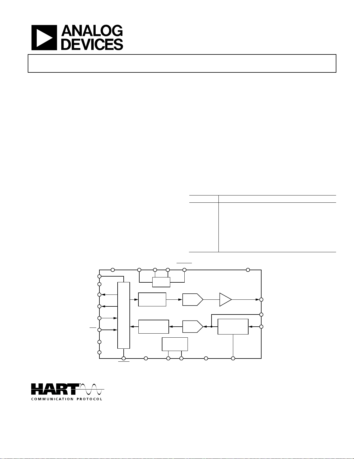
FUNCTIONAL BLOCK DIAGRAM
REG_CAP
CLKOUT
XTAL1
XTAL2
AD5700/AD5700-1
GENERAL DESCRIPTION
The AD5700/AD5700-1 are single-chip solutions, designed
and specified to operate as a HART® FSK half-duplex modem,
complying with the HART physical layer requirements. The
AD5700/AD5700-1 integrate all of the necessary filtering, signal
detection, modulating, demodulating and signal generation
functions, thus requiring few external components. The 0.5%
precision internal oscillator on the AD5700-1 greatly reduces
the board space requirements, making it ideal for line-powered
applications in both master and slave configurations. The maximum supply current consumption is 115 µA, making the AD5700/
AD5700-1 an optimal choice for low power loop-powered applica-
tions. Transmit waveforms are phase continuous 1200 Hz and
2200 Hz sinusoids. The AD5700/AD5700-1 contain accurate
carrier detect circuitry and use a standard UART interface.
Table 1. Related Products
Part No. Description
AD5755-1 Quad-channel, 16-bit, serial input, 4 mA to 20 mA and
AD5421 16-bit, serial input, loop powered, 4 mA to 20 mA DAC
AD5410/
AD5420
AD5412/
AD5422
XTAL_EN
voltage output DAC, dynamic power control, HART
connectivity
Single-channel, 12-bit/16-bit, serial input, 4 mA to 20 mA
current source DACs
Single-channel, 12-bit/16-bit, serial input, current
source and voltage output DACs
CC
IOV
CC
DUPLEX
CD
RXD
TXD
DEMODULATOR
RTS
CLK_CFG0
CLK_CFG1
Rev. A
Information furnished by Analog Devices is believed to be accurate and reliable. However, no
responsibility is assumed by Anal og Devices for its use, nor for any infringements of p atents or other
rights of third parties that may result from its use. Specifications subject to chan ge without notice. No
license is granted by implication or otherwise under any patent or patent rights of Analog Devices.
Trademarks and registered trademarks are the property of their respective owners.
CONTROL L OGIC
RESET
OSC
FSK
MODULATOR
FSK
VO LTAGE
REFERENCE
REF REF_EN AGNDDGND FILTER_SEL
AD5700/AD5700-1
BUFFER
DAC
BAND-PASS
ADC
Figure 1.
One Technology Way, P.O. Box 9106, Norwood, MA 02062-9106, U.S.A.
Tel: 781.329.4700 www.analog.com
Fax: 781.461.3113 ©2012 Analog Devices, Inc. All rights reserved.
FILTER AND
BIASING
HART_OUT
ADC_IP
HART_IN
10435-001

AD5700/AD5700-1 Data Sheet
TABLE OF CONTENTS
Features .............................................................................................. 1
Applications ....................................................................................... 1
General Description ......................................................................... 1
Functional Block Diagram .............................................................. 1
Revision History ............................................................................... 2
Specifications ..................................................................................... 3
Timing Characteristics ................................................................ 5
Absolute Maximum Ratings ............................................................ 6
Thermal Resistance ...................................................................... 6
ESD Caution .................................................................................. 6
Pin Configuration and Function Descriptions ............................. 7
Typical Performance Characteristics ............................................. 9
Terminology .................................................................................... 12
REVISION HISTORY
4/12—Rev. 0 to Rev. A
RTS
Change to Transmit Impedance Parameter,
Changes to Figure 3, Figure 4, Figure 5, and Figure 7 ................. 9
Changes to Figure 10 and Figure 11............................................. 10
Changed AD5755 to AD5755-1 Throughout ............................. 17
Change to Figure 27 ....................................................................... 18
2/12—Revision 0: Initial Version
Low, Table 2 .. 4
Theory of Operation ...................................................................... 13
FSK Modulator ........................................................................... 13
Connecting to HART_OUT ..................................................... 14
FSK Demodulator ...................................................................... 14
Connecting to HART_IN or ADC_IP .................................... 14
Clock Configuration .................................................................. 15
Power-Down Mode .................................................................... 16
Full Duplex Operation ............................................................... 16
Applications Information .............................................................. 17
Supply Decoupling ..................................................................... 17
Typical Connection Diagrams .................................................. 17
Outline Dimensions ....................................................................... 20
Ordering Guide .......................................................................... 20
Rev. A | Page 2 of 20
Data Sheet AD5700/AD5700-1
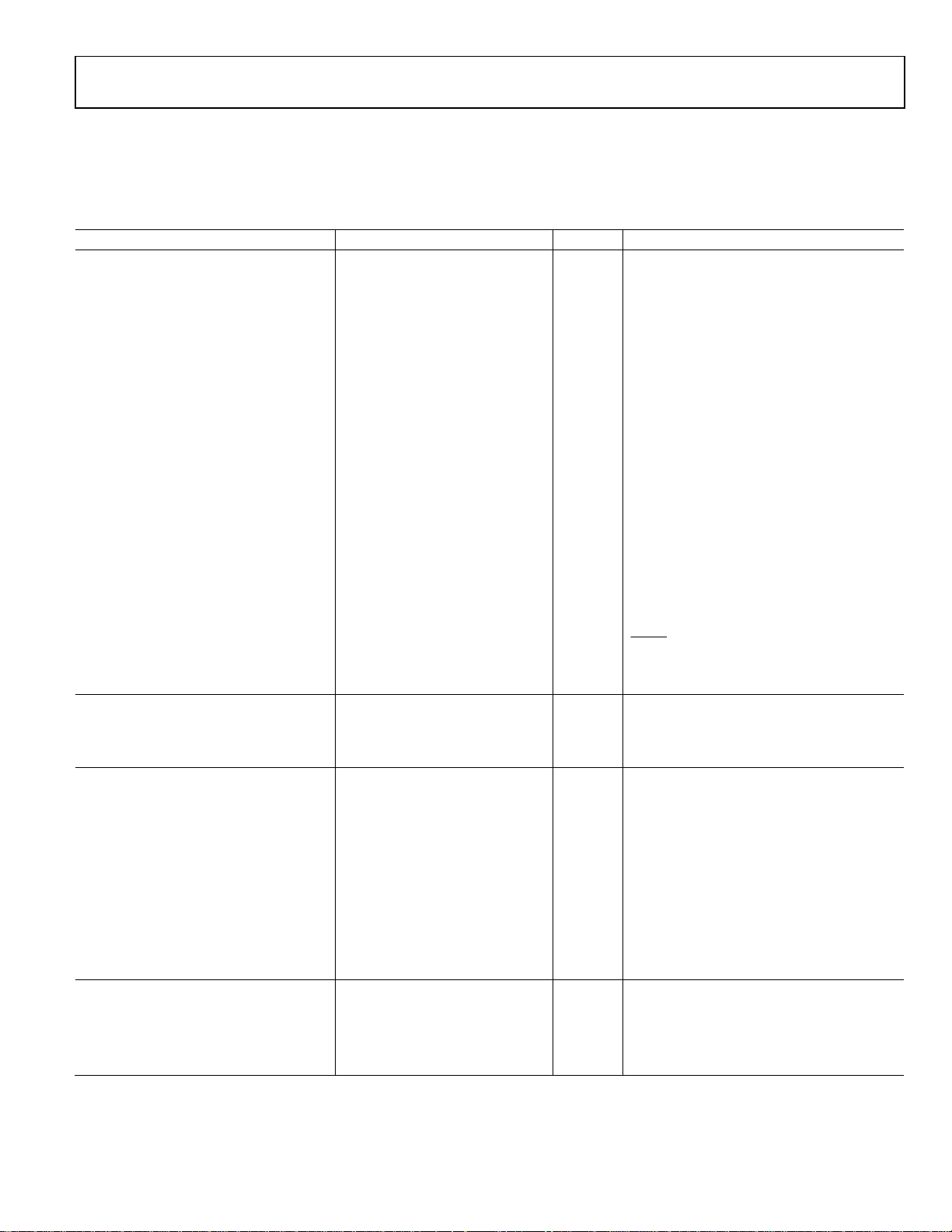
SPECIFICATIONS
VCC = 2 V to 5.5 V, IOVCC = 1.71 V to 5.5 V, AGND = DGND, CLKOUT disabled, HART_OUT with 5 nF load, internal and external
receive filter, internal reference, all specifications are from −40°C to +125°C and relate to both A and B models, unless otherwise noted.
Table 2.
Parameter1 Min Typ Max Unit Test Conditions/Comments
POWER REQUIREMENTS2
VCC 2 5.5 V
IOVCC 1.71 5.5 V
VCC and IOVCC Current Consumption
Demodulator 86 115 μA B model, external clock, −40°C to +85°C
179 μA B model, external clock, −40°C to +125°C
69 97 μA
157 μA
260 μA A model, external clock, −40°C to +125°C
Modulator 124 140 μA B model, external clock, −40°C to +85°C
193 μA B model, external clock, −40°C to +125°C
73 96 μA
153 μA
270 μA A model, external clock, −40°C to +125°C
Crystal Oscillator3 33 60 μA External crystal, 16 pF at XTAL1 and XTAL2
44 71 μA External crystal, 36 pF at XTAL1 and XTAL2
Internal Oscillator4 218 285 μA AD5700-1 only, external crystal not required
Power-Down Mode
VCC and IOVCC Current Consumption 16 35 μA Internal reference disabled, −40°C to +85°C
75 μA Internal reference disabled, −40°C to +125°C
INTERNAL VOLTAGE REFERENCE
Internal Reference Voltage 1.47 1.5 1.52 V
Load Regulation 18 ppm/μA Tested with 50 μA load
OPTIONAL EXTERNAL VOLTAGE
REFERENCE
External Reference Input Voltage 2.47 2.5 2.53 V
External Reference Input Current
Demodulator 16 21 μA
Modulator 28 33 μA
Internal Oscillator 5.5 7 μA
Power-Down 4.6 8.6 μA
DIGITAL INPUTS
VIH, Input High Voltage 0.7 × IOVCC V
VIL, Input Low Voltage 0.3 × IOVCC V
Input Current −0.1 +0.1 μA
Input Capacitance5 5 pF Per pin
B model, external clock, −40°C to +85°C,
external reference
B model, external clock, −40°C to +125 °C,
external reference
B model, external clock, −40°C to +85°C,
external reference
B model, external clock, −40°C to +125°C,
external reference
= REF_EN = DGND
RESET
REF_EN = IOV
reference
REF_EN = DGND to enable use of external
reference, VCC = 2.7 V minimum
Current required by external reference in
receive mode
Current required by external reference in
transmit mode
Current required by external reference if
using internal oscillator
to enable use of internal
CC
Rev. A | Page 3 of 20
AD5700/AD5700-1 Data Sheet
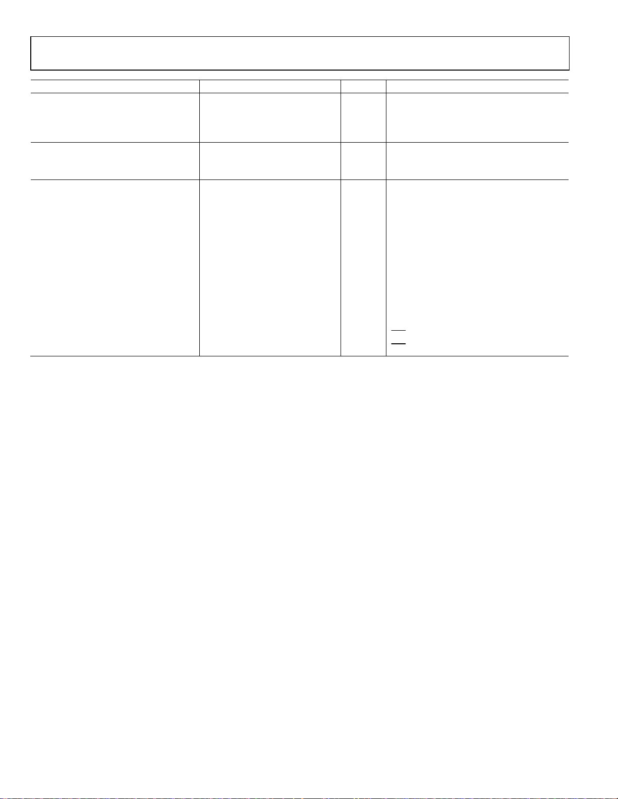
Parameter1 Min Typ Max Unit Test Conditions/Comments
DIGITAL OUTPUTS
VOH, Output High Voltage IOVCC − 0.5 V
VOL, Output Low Voltage 0.4 V
CD Assert6 85 100 110 mV p-p
HART_IN INPUT
Input Voltage Range 0 REF V External reference source
0 1.5 V Internal reference enabled
HART_OUT OUTPUT
Output Voltage 459 493 505 mV p-p
Mark Frequency7 1200 Hz Internal oscillator
Space Frequency7 2200 Hz Internal oscillator
Frequency Error −0.5 +0.5 % Internal oscillator, −40°C to +85°C
−1 +1 % Internal oscillator, −40°C to +125°C
Phase Continuity Error5 0 Degrees
Maximum Load Current5 160 Ω
Transmit Impedance 7 Ω
70 kΩ
1
Temperature range: −40°C to +125°C; typical at 25°C.
2
Current consumption specifications are based on mean current values.
3
The demodulator and modulator currents are specified using an external clock. If using an external crystal oscillator, the crystal oscillator current specification must be
added to the corresponding VCC and IOVCC demodulator/modulator current specification to obtain the total supply current required in this mode.
4
The demodulator and modulator currents are specified using an external clock. If using the internal oscillator, the internal oscillator current specification must be
added to the corresponding VCC and IOVCC demodulator/modulator current specification to obtain the total supply current required in this mode.
5
Guaranteed by design and characterization, but not production tested.
6
Specification set assuming a sinusoidal input signal containing preamble characters at the input and an ideal external filter (see Figure 21).
7
If the internal oscillator is not used, frequency accuracy is dependent on the accuracy of the crystal or clock source used.
5
AC-coupled (2.2 μF), measured at HART_OUT
pin with 160 Ω load (worst-case load), see
Figure 15 and Figure 16 for HART_OUT
voltage vs. load
Worst-case load is 160 Ω, ac-coupled with
2.2 μF, see Figure 19 for recommended
configuration if driving a resistive load
low, at the HART_OUT pin
RTS
high, at the HART_OUT pin
RTS
Rev. A | Page 4 of 20
Data Sheet AD5700/AD5700-1
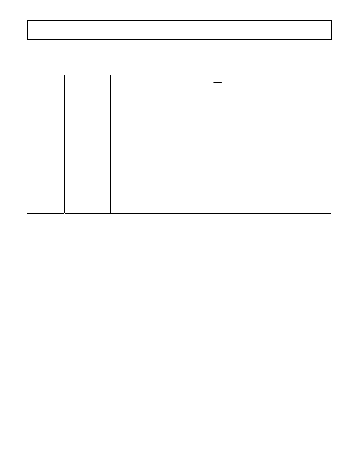
TIMING CHARACTERISTICS
VCC = 2 V to 5.5 V, IOVCC = 1.71 V to 5.5 V, T
Table 3.
Parameter1 Limit at T
MIN
, T
Unit Description
MAX
t1 1 Bit time2 max
t2 1 Bit time2 max
t3 1 Bit time2 max
t4 6 Bit times2 max Carrier detect on. Time from carrier on to CD rising edge. See Figure 5.
t5 6 Bit times2 max Carrier detect off. Time from carrier off to CD falling edge. See Figure 6.
t6 10 Bit times2 max
t7 2.1 ms typ
t8 6 ms typ Crystal oscillator power-up time. Crystal load capacitors = 18 pF.
t9 25 μs typ
t10 10 ms typ Reference power-up time.
t11 30 μs typ
1
Specifications apply to AD5700/AD5700-1 configured with internal or external receive filter.
2
Bit time is the length of time to transfer one bit of data.
MIN
to T
, unless otherwise noted, 1 bit time = 1/1200 Hz = 833.333 µs.
MAX
Carrier start time. Time from RTS
falling edge to carrier reaching its first peak. See
Figure 3.
Carrier stop time. Time from RTS
rising edge to carrier amplitude dropping to ac
zero. See Figure 4.
Carrier decay time. Time from RTS
rising edge to carrier amplitude dropping to ac
zero. See Figure 4.
Carrier detect on when switching from transmit mode to receive mode in the
presence of a constant valid carrier. Time from RTS
rising edge to CD rising edge.
See Figure 7.
Crystal oscillator power-up time. On application of a valid power supply voltage at
or on enabling of the oscillator via the XTAL_EN pin. Crystal load capacitors =
V
CC
8 pF.
Internal oscillator power-up time. On application of a valid power supply voltage
at V
or on enabling of the oscillator via the CLK_CFG0 and CLK_CFG1 pins.
CC
Transition time from power-down mode to normal operating mode (external
clock source, external reference).
Rev. A | Page 5 of 20
AD5700/AD5700-1 Data Sheet
ABSOLUTE MAXIMUM RATINGS
TA = 25°C, unless otherwise noted.
Transient currents of up to 100 mA do not cause SCR latch-up.
Table 4.
Parameter Rating
VCC to GND −0.3 V to +7 V
IOVCC to GND −0.3 V to +7 V
Digital Inputs to DGND −0.3 V to IOVCC + 0.3 V or
Digital Output to DGND −0.3 V to IOVCC + 0.3 V or
HART_OUT to AGND −0.3 V to +2.5 V
HART_IN to AGND −0.3 V to VCC + 0.3 V or
ADC_IP −0.3 V to VCC + 0.3 V or
AGND to DGND −0.3 V to +0.3 V
Operating Temperature Range (TA)
Industrial −40°C to +125°C
Storage Temperature Range −65°C to +150°C
Junction Temperature (TJ
Power Dissipation (TJ
Lead Temperature, JEDEC industry standard
Soldering J-STD-020
ESD
Human Body Model
(ANSI/ESDA/JEDEC JS-001-2010)
Field Induced Charge Model
(JEDEC JESD22_C101E)
Machine Model
(ANSI/ESD S5.2-2009)
) 150°C
MAX
+7 V (whichever is less)
+7 V (whichever is less)
+7 V (whichever is less)
+7 V (whichever is less)
– TA)/θJA
MAX
8 kV
1.5 kV
400 V
Stresses above those listed under Absolute Maximum Ratings
may cause permanent damage to the device. This is a stress
rating only; functional operation of the device at these or any
other conditions above those indicated in the operational
section of this specification is not implied. Exposure to absolute
maximum rating conditions for extended periods may affect
device reliability.
THERMAL RESISTANCE
θJA is specified for the worst-case conditions, that is, a device
soldered in a circuit board for surface-mount packages.
Table 5. Thermal Resistance
Package Type θJA θ
Unit
JC
24-Lead LFCSP 30 3 °C/W
ESD CAUTION
Rev. A | Page 6 of 20
 Loading...