Complete 8-Bit
a
FEATURES
Complete A/D Converter with Reference and Clock
Fast Successive Approximation Conversion: 25 ms
No Missing Codes Over Temperature
08C to +708C: AD570J
–558C to +1258C: AD570S
Digital Multiplexing: Three-State Outputs
18-Pin Ceramic DIP
Low Cost Monolithic Construction
PRODUCT DESCRIPTION
The AD570 is an 8-bit successive approximation A/D converter
consisting of a DAC, voltage reference, clock, comparator, successive approximation register and output buffers—all fabricated
on a single chip. No external components are required to perform a full accuracy 8-bit conversion in 25 µs.
The AD570 incorporates the most advanced integrated circuit
design and processing technology available today. I
grated injection logic) processing in the fabrication of the SAR
function along with laser trimming of the high stability SiCr
thin-film resistor ladder network at the wafer stage (LWT) and a
temperature compensated, subsurface Zener reference insures
full 8-bit accuracy at low cost.
Operating on supplies of +5 V and –15 V, the AD570 accepts
analog inputs of 0 V to +10 V unipolar of ±5 V bipolar, externally selectable. As the BLANK and
low, the three-state outputs go into the high impedance state
and a conversion commences. Upon completion of the conversion, the
the output. Pulling the BLANK and
three states the outputs and readies the device for the next conversion. The AD570 executes a true 8-bit conversion with no
missing codes in approximately 25 µs.
The AD570 is available in two version; the AD570J is specified
for the 0°C to +70°C temperature range, the AD570S for –55°C
to +125°C. Both guarantee full 8-bit accuracy and no missing
codes over their respective temperature ranges.
DATA READY line goes low and the data appears at
CONVERT input is driven
CONVERT input high
2
L (inte-
A-to-D Converter
AD570*
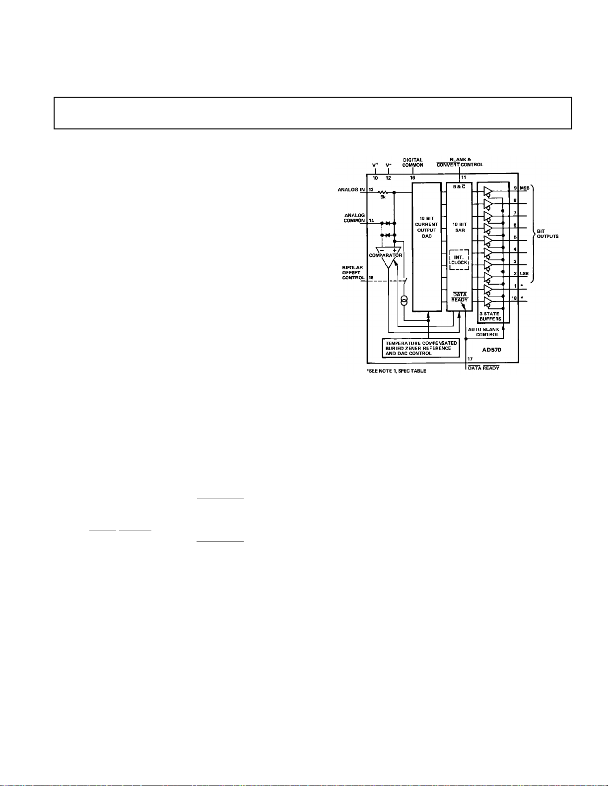
FUNCTIONAL BLOCK DIAGRAM
PRODUCT HIGHLIGHTS
1. The AD570 is a complete 8-bit A/D converter. No external
components are required to perform a conversion. Full-scale
calibration accuracy of ±0.8% (2 LSB of 8 bits) is achieved
without external trims.
2. The AD570 is a single chip device employing the most advanced IC processing techniques. Thus, the user has at his
disposal a truly precision component with the reliability and
low cost inherent in monolithic construction,
3. The AD570 accepts either unipolar (0 V to +10 V) or bipolar
(–5 V to +5 V) analog inputs by grounding or opening a
single pin.
4. The device offers true 8-bit accuracy and exhibits no missing
codes over its entire operating temperature range.
5. Operation is guaranteed with –15 V and +5 V supplies. The
device will also operate with a –12 V supply.
6. The AD570S is also available processed to MIL-STD-883C,
Class B. The military data sheet for the AD570SD/883B is
included in the Analog Devices Military Products Databook.
*U.S. Patents Numbered: 3,940,760; 4,213,806 and 4,136,349.
REV. A
Information furnished by Analog Devices is believed to be accurate and
reliable. However, no responsibility is assumed by Analog Devices for its
use, nor for any infringements of patents or other rights of third parties
which may result from its use. No license is granted by implication or
otherwise under any patent or patent rights of Analog Devices.
One Technology Way, P.O. Box 9106, Norwood, MA 02062-9106, U.S.A.
Tel: 617/329-4700 Fax: 617/326-8703

(TA = +258C, V+ = +5 V, V– = –12 V or –15 V, all voltages measured with respect to
AD570–SPECIFICATIONS
Model Min Typ Max Min Typ Max Units
RESOLUTION
RELATIVE ACCURACY LSB
T
to T
MIN
FULL-SCALE CALIBRATION ±2 ±2 LSB
UNIPOLAR OFFSET 61/2 61/2 LSB
BIPOLAR OFFSET 61/2 61/2 LSB
DIFFERENTIAL NONLINEAIRTY
T
to T
MIN
TEMPERATURE RANGE 0 +70 –55 +125 °C
TEMPERATURE COEFFICIENTS
Unipolar Offset 61 61 LSB
Bipolar Offset 61 61 LSB
Full-Scale Calibration 62 62 LSB
POWER SUPPLY REJECTION
TTL Positive Supply
+4.5 V ≤ V + ≤ +5.5 V 62 62 LSB
Negative Supply
–16.0 V ≤ V – ≤ –13.5 V 62 62 LSB
ANALOG INPUT IMPEDANCE 3.0 5.0 7.0 3.0 5.0 7.0 kΩ
ANALOG INPUT RANGES
Unipolar 0 +10 0 +10 V
Bipolar –5 +5 –5 +5 V
OUTPUT CODING
Unipolar Positive True Binary Positive True Binary
Bipolar Positive True Offset Binary Positive True Offset Binary
LOGIC OUTPUT
Output Sink Current
(V
OUT
Output Source Current
(V
OUT
Output Leakage 640 640 µA
LOGIC INPUTS
Input Current 6100 6100 µA
Logic “1” 2.0 2.0 V
Logic “0” 0.8 0.8 V
CONVERSION TIME 15 25 40 15 25 40 µs
POWER SUPPLY
V+ +4.5 +5.0 +7.0 +4.5 +5.0 +7.0 V
V– –12.0 –15 –16.5 –12.0 –15 –16.5 V
OPERATING CURRENT
V+ 7 10 7 10 mA
V– 9 15 9 15 mA
PACKAGE OPTION
Ceramic
NOTES
1
The AD570 is a selected version of the AD571 10-bit A-to-D converter. Only TTL logic inputs should be connected to Pins 1 and 18 (or no connection made) or
damage may result.
2
For details on grade package offerings for SD-grade in accorance with MIL-STD-883, refer to Analog Devices’ Military Products databook or current /883 data sheet.
Specifications subject to change without notice.
Specifications shown in boldface are tested on all production units at final electrical test. Results from those tests are used to calculate outgoing quality levels. All min
and max specifications are guaranteed, although only those shown in boldface are tested on all production units.
1
MAX
MAX
= 0.4 V max, T
= 2.4 V max, T
2
MIN
MIN
to T
to T
) 3.2 3.2 mA
MAX
) 0.5 0.5 mA
MAX
DIP (D-18) AD570JD AD570SD
digital common, unless otherwise noted)
AD570J AD570S
8 8 Bits
61/2 61/2 LSB
88 Bits
–2–
REV. A

AD570
ABSOLUTE MAXIMUM RATINGS
V+ to Digital Common . . . . . . . . . . . . . . . . . . . . . 0 V to +7 V
V– to Digital Common . . . . . . . . . . . . . . . . . . 0 V to –16.5 V
Analog Common to Digital Common . . . . . . . . . . . . . . . ±1 V
Analog Input to Analog Common . . . . . . . . . . . . . . . . . ±15 V
Control Inputs . . . . . . . . . . . . . . . . . . . . . . . . . . . . . . 0 V to V+
Digital Outputs (Blank Mode) . . . . . . . . . . . . . . . . . . 0 V to V+
Power Dissipation. . . . . . . . . . . . . . . . . . . . . . . . . . . . . 800 mW
CIRCUIT DESCRIPTION
The AD570 is a complete 8-bit A/D converter which requires
no external components to provide the complete successiveapproximation analog-to-digital conversion function. A block
diagram of the AD570 is shown on last page. Upon receipt of
the
CONVERT command, the internal 8-bit current output
DAC is sequenced by the I
2
L successive-approximation register
(SAR) from its most-significant bit (MSB) to least-significant
bit (LSB) to provide an output current which accurately balances the input signal current through the 5 kΩ input resistor.
The comparator determines whether the addition of each successively-weighted bit current causes the DAC current sum to
be greater or less than the input current; if the sum is less the bit
is left on, if more, the bit is turned off. After testing all the bits,
the SAR contains a 8-bit binary code which accurately represents the input signal to within ±1/2 LSB (0.20%).
Upon completion of the sequence, the
DATA READY signal
goes low, and the bit output lines become active high or low
depending on the code in the SAR. When the
BLANK and
CONVERT line is brought high, the output buffers again go
“open”, and the SAR is prepared for another conversion cycle.
The temperature compensated buried Zener reference provides
the primary voltage reference to the DAC and guarantees excellent stability with both time and temperature. The bipolar offset
input controls a switch which allows the positive bipolar offset
current (exactly equal to the value of the MSB less 1/2 LSB)
BIT 2
0.120
BIT 1
MSB
BLANK
&
CONV
BIT 3 BIT 4 BIT 5 BIT 6 BIT 7 BIT 8
V+
LSB
DATA
READY
signal, an input current will be generated which exactly matches
the DAC output with all bits on. (The input resistor is trimmed
slightly low to facilitate user trimming, as discussed on the next
page.)
POWER SUPPLY SELECTION
The AD570 is designed and specified for optimum performance
using a +5 V and –15 V supply. The supply current drawn by
the device is a function of the operating mode (BLANK or
CONVERT), as given on the specification page. The supply
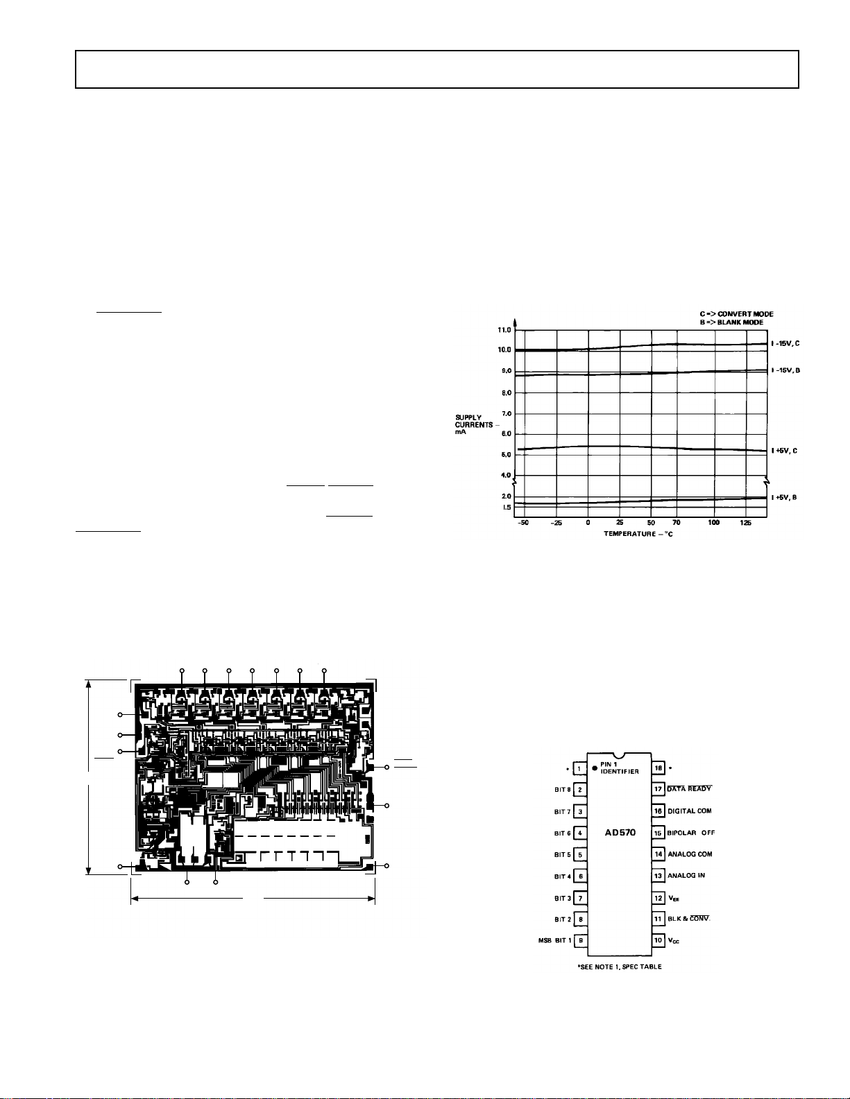
currents change only moderately over temperature as shown in
Figure 2, and do not change significantly with changes in V–
from –10.8 volts to –16 volts.
Figure 2. AD570 Power Supply Current vs. Temperature
CONNECTING THE AD570 FOR STANDARD OPERATION
The AD570 contains all the active components required to perform a complete A/D conversion. Thus, for most situations, all
that is necessary is to connect the power supply (+5 V and –15 V),
the analog input, and the conversion start signal. But, there are
some features and special connections which should be considered for achieving optimum performance. The functional pinout
is shown in Figure 3.
DIGITAL
COMMON
BIPOLAR
V–
ANALOG IN
THE AD570 IS ALSO AVAILABLE IN A LASER-TRIMMED PASSIVATED
CHIP FORM. CONSULT CHIP CATALOG FOR APPLICATION PARTICULARS.
FIGURE 3 SHOWS THE CHIP METALLIZATION LAYOUT AND BONDING PADS.
ANALOG COMMON
0.151
OFFSET
CONTROL
Figure 1. Chip Bonding Diagram
to be injected into the summing (+) node of the comparator to
offset the DAC output. Thus the nominal 0 V to +10 V unipolar input range becomes a –5 V to +5 V range. The 5 kΩ thinfilm input resistor is trimmed so that with a full-scale input
REV. A
–3–
Figure 3. AD570 Pin Connections
 Loading...