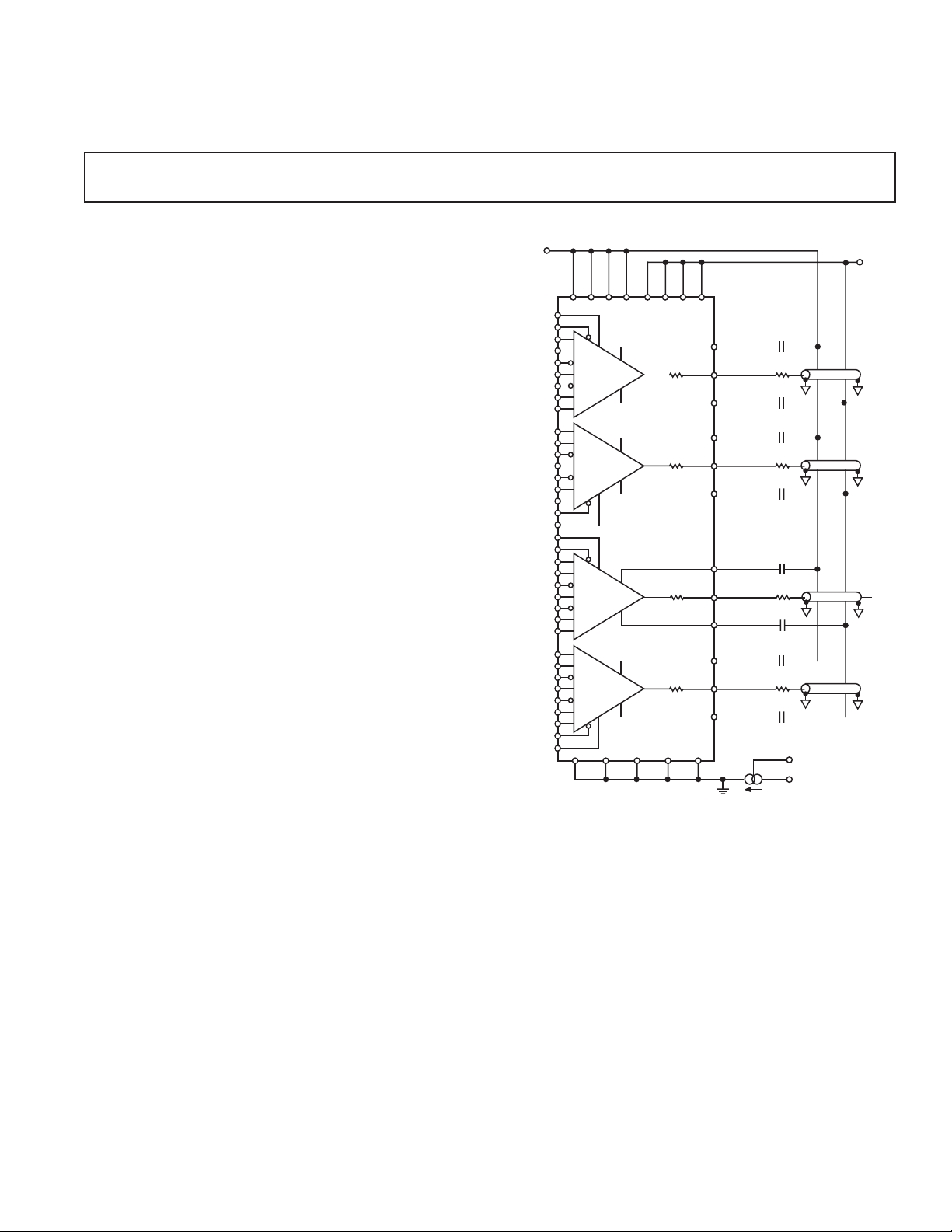
Quad Ultrahigh-Speed Pin Driver
20⍀
ROUT
AD53513
GND
GND
GND
GND
GND
TVCC
THERM
1.0A/K
39nF
39nF
30⍀
50⍀
VCC1
VCC2
VCC3
VCC4
VEE1
VEE2
VEE3
VEE4
VCC
VEE
VH2
DATA2
DATAB2
INH2
INHB2
VL2
VT2
VBB
RLD2
RLD3
VBB
VH3
DATA3
DATAB3
INH3
INHB3
VL3
VT3
VH4
DATA4
DATAB4
INH4
INHB4
VL4
VT4
VBB
RLD4
RLD1
VBB
VH1
DATA1
DATAB1
INH1
INHB1
VL1
VT1
DRIVER 1
VHDCPL1
VOUT1
VLDCPL1
20⍀
ROUT
39nF
39nF
30⍀
50⍀
VHDCPL2
VOUT2
VLDCPL2
DRIVER 2
20⍀
ROUT
39nF
39nF
30⍀
50⍀
VHDCPL3
VOUT3
VLDCPL3
20⍀
ROUT
39nF
39nF
30⍀
50⍀
VHDCPL4
VOUT4
VLDCPL4
DRIVER 4
DRIVER 3
a
FEATURES
500 MHz Driver Operation (1 Gb/s)
Driver Inhibit Function
100 ps Edge Matching
Guaranteed Industry Specifications
20 ⍀ Output Impedance
5 V/ns Slew Rate
Variable Output Voltages for ECL, TTL, and CMOS
High-Speed Differential Inputs for Maximum Flexibility
Ultrasmall 100-Lead LQFP Package with Built-In
Heat Sink
APPLICATIONS
Automatic Test Equipment
Semiconductor Test Systems
Board Test Systems
Instrumentation and Characterization Equipment
PRODUCT DESCRIPTION
The AD53513 is a quad high-speed pin driver designed for use
in digital or mixed-signal test systems. Combining a high-speed
monolithic process with a convenient surface-mount package,
this product attains superb electrical performance while preserving
optimum packaging densities and long-term reliability in a
100-lead, LQFP package with built-in heat sink.
Featuring unity gain programmable output levels of –2.5 V to
+5.5 V, with output swing capability of less than 200 mV to
8 V, the AD53513 is designed to stimulate ECL, TTL, and
CMOS logic families, as well as high-speed memory. The
1.0 Gb/s data rate capacity and matched output impedance
allow for real-time stimulation of these digital logic families.
To test I/O devices, the pin driver can be switched into a high
impedance state (Inhibit Mode), electrically removing the driver
from the path. The pin driver leakage current in inhibit is typically
100 nA and output charge transfer entering inhibit is typically less
than 20 pC.
The AD53513 transition from HI/LO or to inhibit is controlled
through the data and inhibit inputs. The input circuitry uses
high-speed differential inputs with a common-mode range of
± 2 V. This allows for direct interface to precision differential
ECL timing. The analog logic HI/LO inputs are equally easy
to interface. Typically requiring 10 µA of bias current, the
AD53513 can be directly coupled to the output of a digitalto-analog converter.
Each channel of the AD53513 has a Mode Select Pin RLD,
which is a single-sided logic input. The logic threshold is set by
REV. 0
Information furnished by Analog Devices is believed to be accurate and
reliable. However, no responsibility is assumed by Analog Devices for its
use, nor for any infringements of patents or other rights of third parties that
may result from its use. No license is granted by implication or otherwise
under any patent or patent rights of Analog Devices.
with High-Z and V
TERM
Modes
AD53513
FUNCTIONAL BLOCK DIAGRAM
the VBB input which is common to all four channels. The RLD
Mode Select controls whether inhibit puts the driver in High-Z
or V
(DATA, DATAB, INH, INHB, RLD, VBB), must share a
common set of logic levels. The VBB threshold should be set to
the midrange of the logic levels. For example, if ECL levels of
–0.8 V to –1.8 V are used, VBB should be set to –1.3 V.
The AD53513 is available in a 100-lead, LQFP package with a
built-in heat sink and is specified to operate over the ambient
commercial temperature range of –25°C to +85°C.
One Technology Way, P.O. Box 9106, Norwood, MA 02062-9106, U.S.A.
Tel: 781/329-4700 www.analog.com
Fax: 781/326-8703 © Analog Devices, Inc., 2002
mode. (Refer to Table I.) All of the digital logic inputs
TERM

AD53513–SPECIFICATIONS
(All specifications are at TJ = 85ⴗC ⴞ 5ⴗC, +VS = +9 V ⴞ 3%, –VS = –6 V ⴞ 3% unless otherwise noted. All temperature coefficients are measured
at TJ = 75ⴗC–95ⴗC). (A 39 nF capacitor must be connected between VCC and V
Parameter Min Typ* Max Unit Test Conditions
DIFFERENTIAL INPUT CHARACTERISTICS
(Data to DATA, INH to INH), RLD, VBB VBB = –1.3 V
Input Voltage –2 0 Volts
Differential Input Range ECL
Bias Current –1 +1 mA V
VBB Threshold Input Midrange V Set to Midrange of Logic Levels
REFERENCE INPUTS (V
, VH, VT)
L
Bias Currents –50 +50 µAV
OUTPUT CHARACTERISTICS
Logic High Range –2.3 +5.5 Volts DATA = H
Logic Low Range –2.5 +5.3 Volts DATA = L
Amplitude (V
) 0.2 8.0 Volts
H–VL
Absolute Accuracy
Offset –100 +100 mV DATA = H, VH = 0 V, VL = –2 V, VT = +3 V
V
H
V
Gain and Linearity Error ± 0.3 ± 5% of V
H
V
Offset –100 +100 mV DATA = L, VL = 0 V, VH = +5 V, VT = +4.5 V
L
Gain and Linearity Error ± 0.3 ± 5% of V
V
L
Offset –100 +100 mV Term Mode, VT = 0 V, VL = –1 V, VH = +3 V
V
T
V
Gain and Linearity Error ± 0.3 ± 5% of V
T
Offset TC, V
, or VL, or V
H
TERM
± 0.5 mV/°CV
Output Resistance 20 Ω DATA = H, V
Output Leakage –1.0 +1.0 µAV
Dynamic Current Limit 130 mA C
Static Current Limit ± 85 mA Output to –2.5 V, V
PSRR, Drive Mode 35 dB VS = VS ± 3%
DYNAMIC PERFORMANCE, DRIVE
(VH and VL)
Propagation Delay Time 0.3 1.1 ns Measured at 50%, V
Propagation Delay TC ± 0.5 ps/°C Measured at 50%, V
Delay Matching, Edge to Edge 100 ps Measured at 50%, V
Rise and Fall Time
1 V Swing 300 ps Measured 20%–80%, V
2 V Swing 450 ps Measured 10%–90%, V
3 V Swing 650 ps Measured 10%–90%, V
Rise and Fall Time TC
1 V Swing ±1 ps/°C Measured 20%–80%, V
2 V Swing ±1 ps/°C Measured 10%–90%, V
3 V Swing ±1 ps/°C Measured 10%–90%, V
Overshoot, Undershoot, and Preshoot ± (6% +5 0 mV) % of Step + mV a. V
Settling Time
to 15 mV 50 ns V
to 4 mV 10 µsV
Delay Change vs. Pulsewidth 10 ps V
Minimum Pulsewidth
2 V Swing 700 ps 700 ps Input, 10%/90% Output, V
Toggle Rate 3.2 GHz V
–2–
and between VEE and V
HDCPL
= –2 V, 0.0 V
IN
, VH = 2 V
L
+ mV DATA = H, VH = –2 V to +5 V, VL = –2.5 V,
H
+ mV DATA = L, VL = –2 V to +5 V, VH = +5.5 V,
L
+ mV Term Mode, VT = –2.0 V to +5.0 V, VL = 0,
T
= +3 V
V
T
V
= +4.5 V
T
= +3 V
V
H
, VH = 0 V
L
= –2 V to +5 V
OUT
= 39 nF, VH = +5 V, VL = –2 V
BYP
= 0; DATA = H and Output to 5.5 V,
V
T
V
= +5.5 V, VL = –2.5 V, VT = 0
H
= –3 V, DATA = L
V
L
V
= –800 mV
L
V
= –800 mV
L
V
= –800 mV
L
, VH = 0 V, +1 V, VT = –2 V, 50 Ω
L
b. V
, VH = 0 V, +3 V, VT = –2 V, 50 Ω
L
, VH = 0 V, +5 V, VT = –2 V, 50 Ω
c. V
L
= 0 V, VH = +0.5 V, VT = –2 V
L
= 0 V, VH = +0.5 V, VT = –2 V
L
= 0 V, VH = +2 V, VT = –2 V,
L
.)
LDCPL
= 3 V, VL = 0 V, I
H
= +5.5 V, VL = –2.5 V,
H
= 800 mV, 50 Ω Load,
H
= 800 mV, 50 Ω Load,
H
= 800 mV, 50 Ω Load,
H
= 0 V, VH = 1 V, VT = –2 V
L
= 0 V, VH = 2 V, VT = –2 V
L
= 0 V, VH = 3 V, VT = –2 V
L
= 0 V, VH = 1 V, VT = –2 V
L
= 0 V, VH = 2 V, VT = –2 V
L
= 0 V, VH = 3 V, VT = –2 V
L
Pulsewidth/Period = 1.0 ns/4.0 ns, 30 ns/120 ns
= 0 V, VH = +2 V, 50 Ω Terminated
V
L
= –1.8 V, VH = –0.8 V, VT = –2 V,
L
V
> 300 mV p-p at 50 Ω Terminated
OUT
= 45 mA
OUT
= –2 V,
T
REV. 0
 Loading...