Class D/1-Bit Audio Power Output Stage
R
R
AD1991
FEATURES
Class D/1-Bit Audio Power Output Stage
5 V Analog and Digital Supply Voltages
Power Stage Power Supply 8 V to 20 V
Output Power @ 0.1% THD + N
Stereo Mode
2 20 W @ 4 @ 14.4 V
2 20 W @ 8 @ 20 V
Mono Mode
1 40 W @ 4 @ 20 V
< 320 m (per Transistor)
R
ON
Efficiency > 85% @ Full Power/8
Clickless Mute Function
Turn-On and Turn-Off Pop Suppression
Short-Circuit Protection
Overtemperature Protection
Data Loss Protection
2-Channel BTL Outputs or
4-Channel Single-Ended Outputs
52-Lead Exposed Pad TQFP Package
Low Cost DMOS Process
APPLICATIONS
PC Audio Systems
Minicomponents
Automotive Amplifiers
Home Theater Systems
Televisions
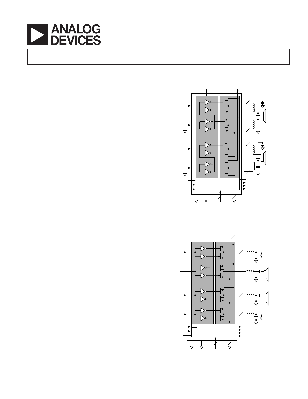
FUNCTIONAL BLOCK DIAGRAMS
2-Channel Mode
INA
LEFT
INPUT
INB
INC
RIGHT
INPUT
IND
CLK
ST/PDN
MUTE
AVDDDV
DD
LEVEL SHIFTER
AND
SWITCH CONTROL
ⴜn
THERMAL PROTECTION
SHORT-CIRCUIT PROTECTION
MUTE CONTROL
AGND DGND
CONTROL
TEST
H-BRIDGE
2 144
A1
A2
B1
B2
C1
C2
D1
D2
PGND
PV
DD
6
4-Channel Mode
OUTA
3
OUTB
3
OUTC
3
OUTD
3
CURRENT OVERLOAD
THERMAL SHUTDOWN
THERMAL WARNING
DATA LOSS
GENERAL DESCRIPTION
The AD1991 is a 2-channel BTL or 4-channel single-ended
class D audio power output stage. The part is configured during
reset to be in either 2-channel mode or 4-channel mode.
To protect the IC as well as the connected speakers, the AD1991
provides turn-on and turn-off pop suppression, short-circuit
protection, and overtemperature shutdown. To control the IC,
a power-down/reset input and a mute pin are available.
The output stage can be operated over a power supply range
from 8 V to 20 V.
In 2-channel mode, Transistors A1, B2, C1, and D2 are turned
on by a Logic 1 on inputs INA and INC, and Transistors A2,
INA
INB
INC
AVDDDV
DD
LEVEL SHIFTER
AND
SWITCH CONTROL
H-BRIDGE
PV
DD
6
A1
OUTA
A2
B1
B2
C1
C2
3
OUTB
3
OUTC
3
LOAD
REQUIRING
DC VOLTAGE
SUPPLY
B1, C2, and D1 are turned on by a Logic 0 on inputs INA and
24 14
TEST
D1
D2
PGND
OUTD
3
CURRENT OVERLOAD
THERMAL SHUTDOWN
THERMAL WARNING
DATA LOSS
LOAD
REQUIRING
DC VOLTAGE
SUPPLY
INC. In 4-channel mode, Transistors A1, B1, C1, and D1 are
turned on by a Logic 1 on the four inputs, and Transistors A2,
IND
B2, C2, and D2 are turned on by a Logic 0 on the four inputs
(see the Functional Block Diagrams).
CLK
ST/PDN
MUTE
REV. 0
Information furnished by Analog Devices is believed to be accurate and
reliable. However, no responsibility is assumed by Analog Devices for its
use, nor for any infringements of patents or other rights of third parties that
may result from its use. No license is granted by implication or otherwise
under any patent or patent rights of Analog Devices. Trademarks and
registered trademarks are the property of their respective companies.
One Technology Way, P.O. Box 9106, Norwood, MA 02062-9106, U.S.A.
Tel: 781/329-4700 www.analog.com
Fax: 781/326-8703 © 2003 Analog Devices, Inc. All rights reserved.
ⴜn
THERMAL PROTECTION
SHORT-CIRCUIT PROTECTION
MUTE CONTROL
AGND DGND
CONTROL

AD1991–SPECIFICATIONS
(AVDD = 5 V, DVDD = 5 V, PV
1
Load Impedance = 8 , unless otherwise noted.)
= 20 V, Ambient Temperature = 25C,
DDX
Parameter Min Typ Max Unit Test Conditions
OUTPUT POWER P
(f = 1 kHz SINE WAVE)
O
EFFICIENCY 87 % f = 1 kHz, P
R
ON
2
20 W RL = 4 Ω, PV
20 W R
= 8 Ω, PV
L
DDX
DDX
= 20 W, RL = 8 Ω
O
Per High-Side Transistor 260 320 mΩ @ 1 A
Per Low-Side Transistor 190 235 mΩ @ 1 A
Temperature Coefficient 0.7 mΩ/°C
THERMAL WARNING ACTIVE 135 °CDie temperature
THERMAL SHUTDOWN ACTIVE 150 °CDie temperature
OVERCURRENT SHUTDOWN ACTIVE 3.8 5 6.75 A
POWER SUPPLIES
Supply Voltage AV
Supply Voltage DV
Supply Voltage PV
DD
DD
DDX
4.5 5.0 5.5 V
4.5 5.0 5.5 V
6.5 8 to 20 22.5 V
Power-Down Current
AV
DV
PV
DD
DD
DDX
614µA RST/PDN held low
113µA RST/PDN held low
17 µA RST/PDN held low
Operating Current
AV
DV
PV
DD
DD
DDX
1.8 2.75 mA
4 5.2 mA
40 mA 50:50 384 kHz square wave on
INA and INC
DIGITAL I/O
Input Voltage High 2.0 DV
DD
V
Input Voltage Low 1.2 V
Output Voltage High DV
– 0.8 V @ 2 mA
DD
Output Voltage Low 0.4 V @ 2 mA
Leakage Current on Digital Inputs 10 µA
NOTES
1
Performance of both channels is identical.
2
Measurement requires PWM modulator.
Specifications subject to change without notice.
= 14 V
= 20 V
DIGITAL TIMING CHARACTERISTICS
(Guaranteed over –40C to +85C, AVDD = DVDD = 5 V 10%, PV
Edge Speed = Slowest, Nonoverlap Time = Shortest.)
= 20 V 10%,
DDX
Symbol Parameter Min Typ Max Unit
t
PDL
t
PST
t
NOL
t
PDRP
t
MSU
t
MH
t
MPDL
Specifications subject to change without notice.
Input transition to output initial response 30 ns
Power transistor switching time 3.5 ns
Nonoverlap time 25 to 40 ns
RST/PDN minimum low pulsewidth 20 ns
Mode pin setup time before RST/PDN going high 5 ns
Mode pin hold time after RST/PDN going high 5 ns
MUTE asserted to output initial response 3 s
REV. 0–2–

AD1991
R
M
INA
OUTA
OUTB
ST/PDN
t
PDL
t
PST
t
PST
t
NOL
t
t
PST
t
PDL
PST
t
NOL
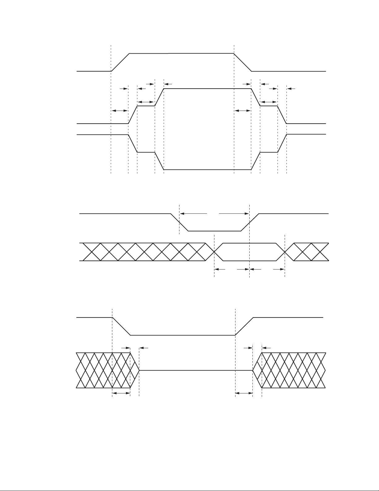
Figure 1. Output Timing
t
PDRP
MODEx
t
MSU
Figure 2.
UTE
t
PST
OUTx
t
MPDL
RESET
Figure 3.
and Mode Timing
MUTE
Timing
t
MPDL
t
MH
t
PST
REV. 0
–3–

AD1991
ABSOLUTE MAXIMUM RATINGS
(TA = 25°C, unless otherwise noted.)
1
AVDD, DVDD to AGND, DGND . . . . . . . . . . –0.3 V to +6.5 V
to PGNDx2 . . . . . . . . . . . . . . . . . . . –0.3 V to +30.0 V
PV
DDX
AGND to DGND to PGNDx . . . . . . . . . . . . –0.3 V to +0.3 V
to DVDD . . . . . . . . . . . . . . . . . . . . . . . –0.5 V to +0.5 V
AV
DD
Operating Temperature Range (Ambient)
Industrial . . . . . . . . . . . . . . . . . . . . . . . . . –40°C to +85°C
Storage Temperature Range . . . . . . . . . . . . –65°C to +150°C
Maximum Junction Temperature . . . . . . . . . . . . . . . . . 150°C
Thermal Resistance3 . . . . . . . . . . . . . . . . . . . . . . . 1°C/W
θ
JC
Lead Temperature
Soldering (10 sec) . . . . . . . . . . . . . . . . . . . . . . . . . . . 260°C
Vapor Phase (60 sec) . . . . . . . . . . . . . . . . . . . . . . . . . 215°C
Infrared (15 sec) . . . . . . . . . . . . . . . . . . . . . . . . . . . . 220°C
ORDERING GUIDE
Temperature Package Package
Model Range Description Option
AD1991ASV –40°C to +85°CThin Quad Flat Pack [TQFP] SV-52
AD1991ASVRL –40°C to +85°CThin Quad Flat Pack [TQFP] SV-52
EVAL-AD1991EB Evaluation Board
NOTES
1
Stresses above those listed under Absolute Maximum Ratings may cause permanent damage to the device. This is a stress rating only; functional operation of the
device at these or any other conditions above those listed in the operational
sections of this specification is not implied. Exposure to absolute maximum rating
conditions for extended periods may affect device reliability. Only one absolute
maximum rating may be applied at any one time.
2
Including any induced voltage due to inductive load.
3
With respect to the temperature of the exposed pad.
CAUTION
ESD (electrostatic discharge) sensitive device. Electrostatic charges as high as 4000 V readily
accumulate on the human body and test equipment and can discharge without detection. Although the
AD1991 features proprietary ESD protection circuitry, permanent damage may occur on devices
subjected to high energy electrostatic discharges. Therefore, proper ESD precautions are recommended
to avoid performance degradation or loss of functionality.
REV. 0–4–
 Loading...