Audio Switching Amplifier
FEATURES
Integrated stereo modulator and power stage
<0.002% THD + N
101 dB dynamic range (A-weighted)
2 × 5 W output power (4 Ω, <0.01% THD + N)
< 0.3 Ω (per transistor)
R
DS-ON
PSRR > 65 dB
On-off-mute pop noise suppression
EMI optimized modulator
Short-circuit protection
Overtemperature protection
Low cost DMOS process
APPLICATIONS
Advanced televisions
Compact multimedia systems
Minicomponents
PGA1 PGA0
AV
GENERAL DESCRIPTION
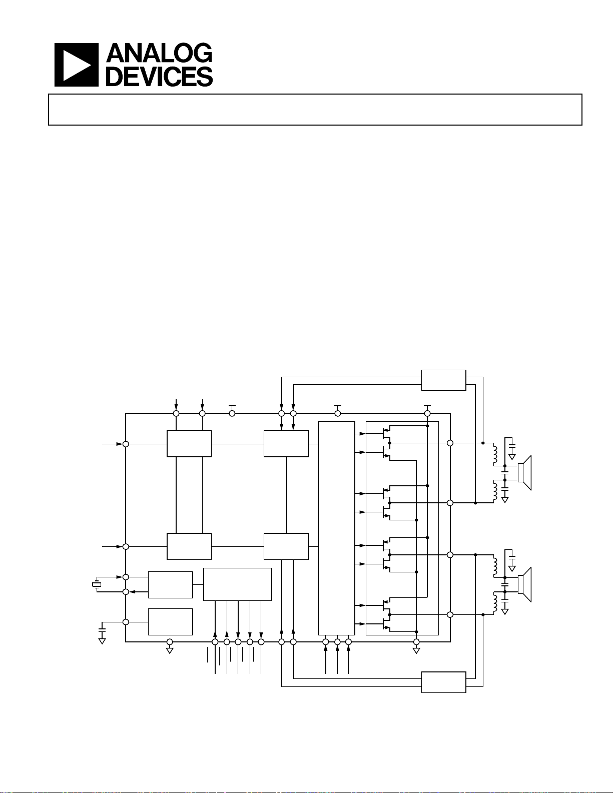
The AD1990 is a 2-channel, bridge tied load (BTL), switching
audio power amplifier with integrated Σ-Δ modulator. The
modulator accepts a single-ended, analog input signal and
converts it to a switching waveform to drive speakers directly. A
digital, microprocessor-compatible interface provides control of
reset, mute, and PGA gain, as well as feedback signals for thermal
and overcurrent error conditions. The output stage can operate
over a power supply voltages range of 8 V to 12 V. The analog
modulator and digital logic operate from a 5 V supply.
FUNCTIONAL BLOCK DIAGRAM
NFL–
DD
NFL+
DV
DD
FEEDBACK
NETWO RK
PV
DD
AD1990
AINL
AINR
CLKI
CLKO
REF_FILT
AD1990
OSCILLATOR
REFERENCE
VOLTAGE
AGND
PGA
PGA
MODE CONT ROL
LOGI C AND
POP/CLICK
SUPPRESSION
ERR2
MUTE
ERR1
RESET
MODULAT OR
MODULAT OR
ERR0
Σ-Δ
LEVEL
SHIFTER
AND
DEAD TIME
CONTROL
Σ-Δ
NFR–
NFR+
DCTRL2
DCTRL1
DCTRL0
A1
A2
B1
B2
H-BRIDGE
C1
C2
D1
D2
PGND
Figure 1.
FEEDBACK
NETWO RK
OUTL+
OUTL–
OUTR+
OUTR–
05380-001
Rev. 0
Information furnished by Analog Devices is believed to be accurate and reliable. However, no
responsibility is assumed by Anal og Devices for its use, nor for any infringements of patents or ot her
rights of third parties that may result from its use. Specifications subject to change without notice. No
license is granted by implication or otherwise under any patent or patent rights of Analog Devices.
Trademarks and registered trademarks are the property of their respective owners.
One Technology Way, P.O. Box 9106, Norwood, MA 02062-9106, U.S.A.
Tel: 781.329.4700 www.analog.com
Fax: 781.461.3113 ©2006 Analog Devices, Inc. All rights reserved.

AD1990
TABLE OF CONTENTS
Features .............................................................................................. 1
Overview ..................................................................................... 11
Applications....................................................................................... 1
General Description ......................................................................... 1
Functional Block Diagram .............................................................. 1
Revision History ............................................................................... 2
Specifications..................................................................................... 3
Absolute Maximum Ratings............................................................ 5
ESD Caution.................................................................................. 5
Pin Configuration and Function Descriptions............................. 6
Typical Performance Characteristics ............................................. 8
Theory of Operation ...................................................................... 11
REVISION HISTORY
4/06—Revision 0: Initial Version
Σ-Δ Modulator............................................................................ 11
and
RESET
..................................................................... 11
MUTE
Gain Structure............................................................................. 11
Power Stage ................................................................................. 13
Clocking....................................................................................... 13
Protection Circuits and Error Reporting ................................ 14
Application Circuits ....................................................................... 15
Outline Dimensions ....................................................................... 16
Ordering Guide .......................................................................... 16
Rev. 0 | Page 2 of 16

AD1990
SPECIFICATIONS
Test conditions, unless otherwise specified.
Table 1.
Parameter Ratings
SUPPLY VOLTAGES
AV
DD
DV
DD
PV
DD
AMBIENT TEMPERATURE 25°C
LOAD IMPEDANCE 6 Ω
CLOCK FREQUENCY 12.288 MHz
PGA GAIN 0 dB
MEASUREMENT BANDWIDTH 20 Hz to 20 kHz
Table 2.
Parameter Min Typ Max Unit Test Conditions/Comments
R
DS-ON
Per High-Side Transistor 260 355 mΩ T = 25°C
Per Low-Side Transistor 210 265 mΩ T = 25°C
MAXIMUM CURRENT THROUGH OUTx 5 A Peak
THERMAL WARNING ACTIVE 135 °C Die temperature
THERMAL SHUTDOWN ACTIVE 150 °C Die temperature
RESTORE TEMPERATURE AFTER THERMAL SHUTDOWN 120 °C Die temperature
Table 3. Performance Specifications
Parameter Typ Unit Test Conditions/Comments
TOTAL HARMONIC DISTORTION AND NOISE (THD + N) 0.003 % PGA = 0 dB, PO = 1 W, 1 kHz
0.006 % PGA = 6 dB, PO = 1 W, 1 kHz
0.01 % PGA = 12 dB, PO = 1 W, 1 kHz
0.02 % PGA = 18 dB, PO = 1 W, 1 kHz
SIGNAL-TO-NOISE RATIO (SNR) 102 dB 1 kHz, A-weighted, 0 dB referred to 1% THD + N output
DYNAMIC RANGE (DNR) 102 dB 1 kHz, A-weighted, −60 dB referred to 1% THD + N output
CROSSTALK (LEFT-TO-RIGHT OR RIGHT-TO-LEFT) −100 dB PGA = 0 dB, PO = 5 W, 1 kHz
Table 4. DC Specifications
Parameter Typ Unit Test Conditions/Comments
INPUT IMPEDANCE 20 kΩ AINL, AINR input pins
OUTPUT DC OFFSET ±4 mV Independent of PGA setting
5 V
5 V
12 V
Rev. 0 | Page 3 of 16

AD1990
Table 5. Power Supplies
Parameter Min Typ Max Unit Test Conditions/Comments
ANALOG SUPPLY, AV
DIGITAL SUPPLY, DV
POWER TRANSISTOR SUPPLY, PV
DD
DD
DD
RESET/POWER-DOWN CURRENT
AV
DD
DV
DD
PV
DD
QUIESCENT CURRENT Inputs grounded, nonoverlap = minimum
AV
DD
DV
DD
PV
DD
OPERATING CURRENT VIN = 1 V rms, RL = 6 Ω, PO = 1 W
AV
DD
DV
DD
PV
DD
Table 6. Digital I/O
Parameter Min Typ Max Unit Test Conditions/Comments
INPUT LOGIC HIGH 2.0 V
INPUT LOGIC LOW 0.8 V
OUTPUT LOGIC HIGH 2.4 V @ 4 mA
OUTPUT LOGIC LOW 0.4 V @ 4 mA
LEAKAGE CURRENT ON DIGITAL OUTPUTS 10 μA
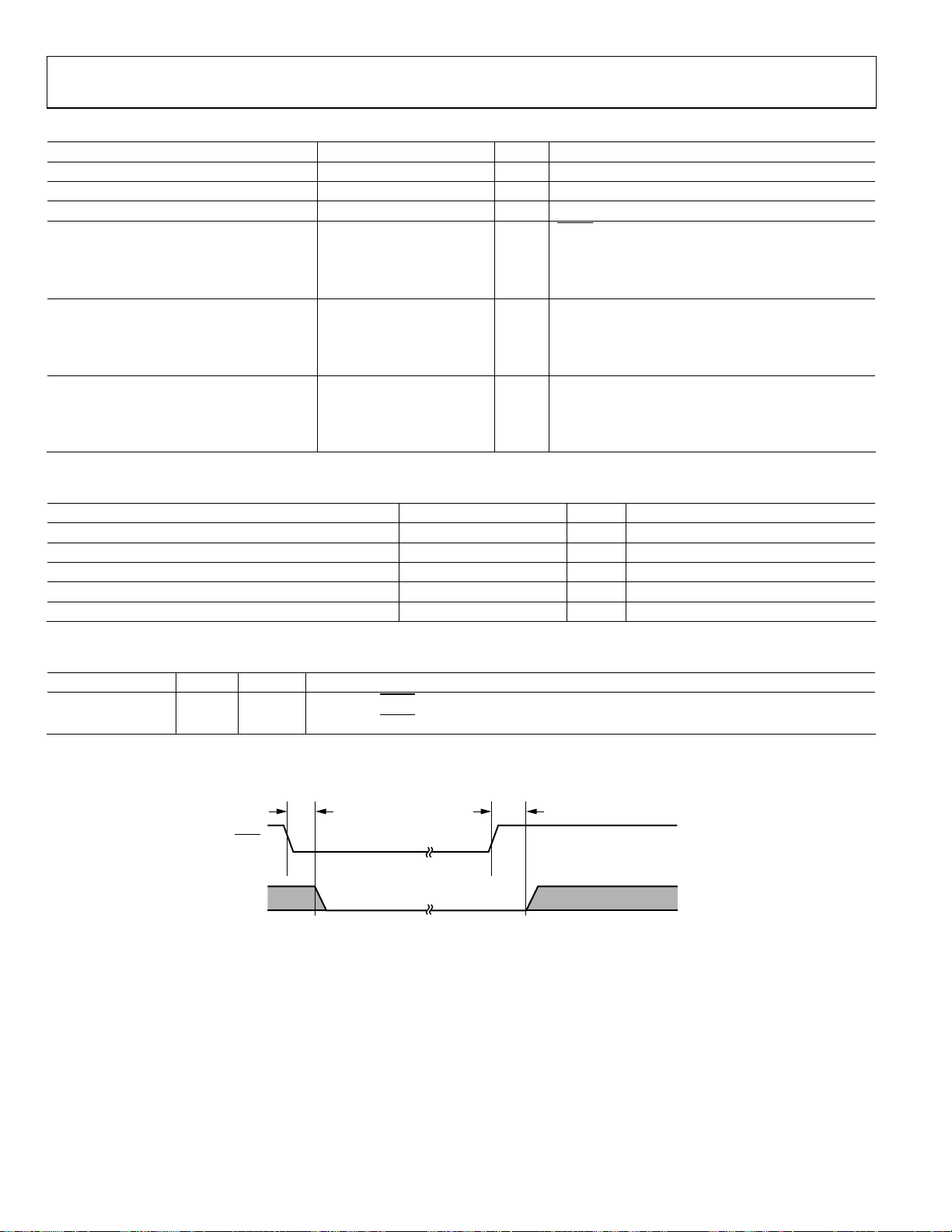
Table 7. Digital Timing
Parameter Typ Unit Test Conditions/Comments
t
MD
t
UD
10 μs
34 μs
4.5 5.0 5.5 V
4.5 5.0 5.5 V
6.5 8 to 12 15 V
RESET held low
0.6 1 μA 5 V
7.5 11 μA 5 V
19 40 μA 12 V
20 mA 5 V
5.5 mA 5 V
30 mA 12 V
20 27 mA 5 V
5.5 7 mA 5 V
218 260 mA 12 V
Delay after
Delay after
MUTE is asserted until output stops switching
MUTE is deasserted until output starts switching
t
UD
05380-002
MUTE
OUTx
t
MD
Figure 2. Mute and Unmute Delay Timing
Rev. 0 | Page 4 of 16

AD1990
ABSOLUTE MAXIMUM RATINGS
Table 8.
Parameter Rating
AVDD, DVDD to AGND, DGND −0.3 V to +6.5 V
PVDDx to PGNDx
AGND to DGND to PGNDx −0.3 V to +0.3 V
AVDD, to DVDD −0.5 V to +0.5 V
Operating Temperature Range –40°C to +85°C
Storage Temperature Range –65°C to +150°C
Maximum Junction Temperature 150°C
Thermal Resistance
θ
JA
θJC (at the Exposed Pad Surface) 0.9°C/W
θJB (on JEDEC Standard PCB) 9.7°C/W
1
Including any induced voltage due to inductive load.
1
−0.3 V to +22.5 V
19.2°C/W
Stresses above those listed under Absolute Maximum Ratings
may cause permanent damage to the device. This is a stress
rating only; functional operation of the device at these or any
other conditions above those indicated in the operational
section of this specification is not implied. Exposure to absolute
maximum rating conditions for extended periods may affect
device reliability.
ESD CAUTION
ESD (electrostatic discharge) sensitive device. Electrostatic charges as high as 4000 V readily accumulate on
the human body and test equipment and can discharge without detection. Although this product features
proprietary ESD protection circuitry, permanent damage may occur on devices subjected to high energy
electrostatic discharges. Therefore, proper ESD precautions are recommended to avoid performance
degradation or loss of functionality.
Rev. 0 | Page 5 of 16
 Loading...