High Definition Audio
ADC0
ADC1
AD1989B
GPIO
AND
EAPD
ADC2
6
6
6
6
6
6
6
6
PORT C
PORT B
PORT A
PORT E
PORT D
PORT G
PORT F
MONO OUT
6
S/PDIF Tx
S/PDIF Tx
S/PDIF Rx
H
D
A
U
D
I
O
I
N
T
E
R
F
A
C
E
DIGITAL
AND ANALOG
PCBEEP
DAC0
DAC1
DAC2
DAC3
6
PORT H
DAC4
S/PDIF OUT 1
S/PDIF OUT 2 (HDMI)
S/PDIF IN
http://www.BDTIC.com/ADI
SoundMAX Codec
AD1989B
FEATURES
Ten 192 kHz, 101 dB DACs
7.1 surround sound plus independent headphone
All independent sample rates, 8 kHz through 192 kHz
Selectable stereo mixer on outputs
16-, 20-, and 24-bit resolution
Six 192 kHz, 92 dB ADCs
Simultaneous record of up to 3 stereo channels
All independent sample rates, 8 kHz through 192 kHz
16-, 20-, and 24-bit resolution
S/PDIF output
2 independent transmitters, second S/PDIF can support
external HDMI interface
Supports 44.1 kHz through 192 kHz sample rates
16-, 20-, and 24-bit data; PCM, and AC3 formats
Digital PCM gain control
S/PDIF input
Supports 44.1 kHz through 192 kHz sample rates
16-, 20-, and 24-bit data; PCM, and AC3 formats
Digital PCM gain control
Auto synchronizes to source sample rate
Dedicated auxiliary pins
Stereo CD/auxiliary I/O port w/GND sense
MONO_OUT pin for internal speaker with EAPD support
Microsoft Vista Premium
®
logo compliant
Support up to 9 audio jacks
Impedance and presence detection; retasking
5 adjustable microphone bias pins
Digital and analog PCBeep
3 general-purpose digital I/O (GPIO) pins
Multiple EAPD pins for external circuit control
3.3 V analog and digital supply voltages
1.5 V and 3.3 V HD Audio link signaling
Advanced power management modes
Rev. 0
Information furnished by Analog Devices is believed to be accurate and reliable.
However, no responsibility is assumed by Analog Devices for its use, nor for any
infringements of patents or other rights of third parties that may result from its use.
Specifications subject to change without notice. No license is granted by implication
or otherwise under any patent or patent rights of Analog Devices. Trademarks and
registered trademarks are the property of their respective owners.
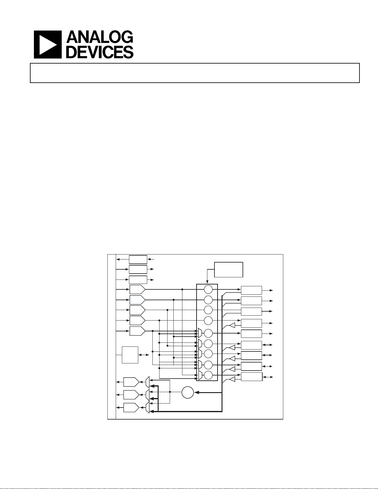
Figure 1. AD1989B Block Diagram
One Technology Way, P.O. Box 9106, Norwood, MA 02062-9106 U.S.A.
Tel: 781.329.4700 www.analog.com
Fax: 781.461.3113 ©2008 Analog Devices, Inc. All rights reserved.

AD1989B
http://www.BDTIC.com/ADI
CONTENTS
Features ................................................................. 1
Contents ................................................................ 2
Revision History ...................................................... 2
General Description ................................................. 3
Special Software Features ........................................ 3
Additional Information .......................................... 3
Jack Configuration ................................................ 3
Specifications .......................................................... 4
Test Conditions .................................................... 4
Performance ........................................................ 4
General Specifications ............................................ 4
HD Audio Link Specification ................................... 7
Power-Down States ............................................... 7
Absolute Maximum Ratings .................................... 8
ESD Caution ........................................................ 8
Environmental Conditions ...................................... 8
Pin Configuration and Function Descriptions ................. 9
HD Audio Widgets ................................................ 12
HD Audio Parameters ............................................. 14
Widget Parameters ................................................. 15
Connection List ..................................................... 17
Default Configuration Bytes ..................................... 19
Outline Dimensions ............................................... 20
Ordering Guide ..................................................... 20
REVISION HISTORY
8/08—Revision 0: Initial Version
Rev. 0 | Page 2 of 20 | August 2008

GENERAL DESCRIPTION
http://www.BDTIC.com/ADI
AD1989B
The AD1989B audio codec and SoundMAX® software provides
superior HD audio quality that exceeds Vista Premium performance. The AD1989B has ten 101 dB DACs and six 92 dB
ADCs, three stereo headphone ports, C/LFE swapping, digital
and analog PCBeep, and two independent S/PDIF outputs,
making the AD1989B the right choice for PCs where performance and a rich feature set are primary considerations.
The jack retasking feature on this product supports various configurations including 7.1 on 5 jacks, 5.1 on 3 jacks, and front
panel jack retasking.
The AD1989B is available in a 48-lead RoHS compliant lead
frame chip scale package in both reels and trays. See Ordering
Guide on Page 20.
SPECIAL SOFTWARE FEATURES
The AD1989B audio codec also supports the following additional software features:
•BlackHawk
controls
• Voice input enhancement: Andrea Electronics best-in-class
noise reduction, beam forming, and echo cancellation
• Output enhancement: Sensaura/Sonic Focus, spreading/downmixing, MP3 refinement, adaptive dynamics,
compressor/limiter, speaker/graphic EQ, Voice Clarity/
X-Matrix
•DTS
®
and SoundMAX GUI contain all user audio
TM
, AGC, UI tuning tools
®
, SRS®, EAX® for gaming
JACK CONFIGURATION
The guidelines shown in Table 1 and Table 2 should be used
when selecting ports for particular functions.
Table 1. Typical Desktop Applications with Discreet Jacks
(Default Configuration)
Port Function
Port A Front Panel Headphone
Port B Front Panel Microphone
Port C Rear Line-In
Port D Rear Line-Out
Port E Rear Microphone
Port F Rear Surround (5.1)
Port G Rear C/LFE
Port H Rear Surround (7.1)
Table 2. Typical Desktop Retasking to Support Input/5.1 on
3 Jacks
Port Function
Port A Front Panel Headphone
Port B Front Panel Microphone
Port C Rear Line-In/Surround Out
Port D Rear Line-Out
Port E Rear Microphone/C/LFE
ADDITIONAL INFORMATION
This data sheet provides a general overview of the AD1989B
SoundMAX codec’s architecture and functionality. Additional
information on the AD1989B is available in the AD1989B Programmers Reference Manual. Please contact your local Analog
Devices, Inc., sales representative for more information. For
information on SoundMAX codecs and software, see Analog
Devices website at http://www.analog.com/soundMAX.
Rev. 0 | Page 3 of 20 | August 2008

AD1989B
http://www.BDTIC.com/ADI
SPECIFICATIONS
TEST CONDITIONS
Parameter Test Condition
Tem pe ra tu re
Digital Supply
Analog Supply
MIC_BIAS_IN (via Low-Pass Filter)
Sample Rate f
S
Input Signal (Frequency Sine Wave)
Amplitude for THD + N
Analog Output Pass Band
DAC 10 kΩ Output Load: Line-Out Tests
ADC 0 dB Gain
PERFORMANCE
Parameter Min Typ Max Unit
Line-Out Drive (10 kΩ loads—DAC to Pin)
Total Harmonic Distortion (THD + N)
Dynamic Range (–60 dB in ref to fS A-Weighted)
Signal-to-Noise Ratio
Headphone Drive (32 Ω loads—DAC to Pin)
Total Harmonic Distortion (THD + N)
Dynamic Range (–60 dB in ref to f
Signal-to-Noise Ratio
Input Ports (Mic Boost = 0 dB)
Total Harmonic Distortion (THD + N)
Dynamic Range (–60 dB in ref to f
Signal-to-Noise Ratio
25°C
3.3 V
3.3 V
5.0 V
48 kHz
1008 Hz
–3.0 dB Full Scale
20 Hz to 20 kHz
32 Ω Output Load: Headphone Tests
A-Weighted)
S
A-Weighted)
S
–86
101
101
–84
101
101
–80
92
92
dB
dB
dB
dB
dB
dB
dB
dB
dB
GENERAL SPECIFICATIONS
Parameter Min Typ Max Unit
DIGITAL DECIMATION AND INTERPOLATION FILTERS—fS = 8 kHz to 96 kHz
Pass Band 0 0.4 f
Pass-Band Ripple ±0.005 dB
Stop Band 0.6 f
Stop-Band Rejection –110 dB
Group Delay 20 1/f
Group Delay Variation Over Pass Band 0 μs
ANALOG-TO-DIGITAL CONVERTERS
Resolution 24 Bits
Gain Error (Full-Scale Span Relative to Nominal Input Voltage)
Interchannel Gain Mismatch (Difference of Gain Errors) ±0.2 ±0.5 dB
ADC Offset Error
ADC Crosstalk
1
1
2
Line Inputs (Input L, Ground R, Read R; Input R, Ground L, Read L) –94 dB
Line Inputs to Other –100 –80 dB
DIGITAL-TO-ANALOG CONVERTERS
Resolution 24 Bits
Gain Error (Full-Scale Span Relative to Nominal Input Voltage)
1
Interchannel Gain Mismatch (Difference of Gain Errors) ±0.5 dB
DAC Crosstalk (Input L, Zero R, Measure R_OUT; Input R, Zero L, Measure L_OUT)
1
S
S
Hz
Hz
±10 %
±5mV
±10 %
1
–104 dB
S
Rev. 0 | Page 4 of 20 | August 2008

AD1989B
http://www.BDTIC.com/ADI
Parameter Min Typ Max Unit
DAC VOLUMES
Step Size (DAC0, DAC1, DAC2, DAC3) 1.5 dB
Output Gain/Attenuation Range –58.5 0 dB
Mute Attenuation of 0 dB Fundamental
ADC VOLUMES
Step Size (ADCSEL-0, ADCSEL-1) 1.5 dB
PGA Gain/Attenuation Range –58.5 +22.5 dB
Mute Attenuation of 0 dB Fundamental
ANALOG MIXER
Signal-to-Noise Reduction (SNR) Input to Output 95 dB
Step Size: All Mixer Inputs –1.5 dB
Input Gain/Attenuation Range: All Mixer Inputs –34.5 +12.0 dB
ANALOG LINE LEVEL OUTPUTS
Full-Scale Output Voltage: Line-Out Drive Enabled 1.0 V rms
ANALOG HP DRIVE OUTPUTS
Full-Scale Output Voltage: Line-Out Drive Enabled 1.0 V rms
Ports A, B and D (when HP Drive is Enabled) 2.83 V p-p
ANALOG INPUTS
Input Voltages—Ports A, B, C, or E
Input Voltages—Microphone Boost
Amplifier, Ports B, C, or E
Input Impedance
PCBEEP
Ports A, B, C, E (Mic Boost = 0 dB)
Input Capacitance
1
MICROPHONE BIAS
MIC_BIAS-B, MIC_BIAS-C
MIC_BIAS_IN (Pin 33) = +5 V or +3.3 V V
V
V
MIC_BIAS_IN (Pin 33) = +5 V V
V
MIC_BIAS_IN (Pin 33) = +3.3 V V
1
1
Output Impedance
External Load Impedance
Output Capacitance
External Load Capacitance
Output Impedance
External Load Impedance
Output Capacitance
External Load Capacitance
1
1
1
1
1
1
1
1
10 kΩ
32 Ω
–80 dB
–80 dB
190 Ω
15 pF
1000 pF
0.5 Ω
15 pF
1000 pF
Mic Boost = 0 dB 1
2.83
Mic Boost = +10 dB 0.316
0.894
Mic Boost = +20 dB 0.1
0.283
Mic Boost = +30 dB 0.032
0.089
23
150
57.5pF
Setting = High-Z High-Z
REF
Setting = 0 V 0 V dc
REF
Setting = 50% 1.65 V dc
REF
Setting = 80% 3.7 V dc
REF
Setting = 100% 3.9 V dc
REF
Setting = 80% 2.86 V dc
REF
V
Setting = 100% 3.0 V dc
REF
V rms
V p-p
V rms
V p-p
V rms
V p-p
V rms
V p-p
kΩ
kΩ
3
3
3
3
3
3
MIC_BIAS-E (When enabled as BIAS) V
Output Drive Current V
Setting = High-Z High-Z
REF
V
Setting = 0 V 0 V dc
REF
V
Setting = 50% 1.65 V dc
REF
V
Setting = 80% 2.86 V dc
REF
V
Setting = 100% 3.0 V dc
REF
Setting = 50%, 80%, or 100% 1.6 mA
REF
Rev. 0 | Page 5 of 20 | August 2008

AD1989B
http://www.BDTIC.com/ADI
Parameter Min Typ Max Unit
GPIO_0, GPIO_1, and GPIO_2
Input Signal High (V
Input Signal Low (V
Output Signal High (V
Output Signal Low (V
Input Leakage Current (Signal High) (IIH) –150 nA
Input Leakage Current (Signal Low) (I
S/PDIF-Out_1, S/PDIF-Out_2
Output Signal High (V
Output Signal Low (V
S/PDIF_IN
Input Signal High (V
Input Signal Low (V
Input Leakage Current (Signal High) (I
Input Leakage Current (Signal Low) (I
POWER SUPPLY
Analog (AV
) 3.3 V ± 5%
DD
Power Supply Range
Power Dissipation
Supply Current
Digital (DV
) 3.3 V ± 10%
DD
Power Supply Range
Power Dissipation
Supply Current
Digital I/O (DV
IO
Power Supply Range
Power Dissipation
Supply Current
Digital I/O (DVIO) 1.5 V ± 5.5%
Power Supply Range
Power Dissipation
Supply Current
Digital GPIO (DV
Power Supply Range
Power Dissipation
Supply Current
Power Supply Rejection (Reference to f
1
Guaranteed but not tested.
2
Measurements reflect main ADC.
3
RMS values assume sine wave input.
)DV
IH
)0DV
IL
) I
OH
)I
OL
IL
) I
OH
)I
OL
)DV
IH
)0DV
IL
IH
)–50μA
IL
= –500 μADV
OUT
= +1500 μA0 DV
OUT
)–50μA
= –500 μADV
OUT
= +1500 μA0 DV
OUT
) 150 nA
× 0.60 DV
GPIO
× 0.72 DV
GPIO
× 0.72 DV
GPIO
× 0.60 DV
GPIO
3.13 3.30
162
49
2.97 3.30
241
73
GPIO
× 0.24 V
GPIO
GPIO
× 0.10 V
GPIO
GPIO
× 0.10 V
GPIO
GPIO
× 0.24 V
GPIO
3.46 V
3.63 V
V
V
V
V
mW
mA
mW
mA
) 3.3 V ± 10%
) 3.3 V ± 10%
GPIO
2.97 3.30
0.66
0.20
1.42 1.50
0.03
0.20
2.97 3.30
3.63
1.10
100 mV p-p Signal @ 1 kHz)1 80 dB
S
3.63 V
mW
mA
1.58 V
mW
mA
3.63 V
mW
mA
Rev. 0 | Page 6 of 20 | August 2008
 Loading...