Analog Devices AD1862 Datasheet

Ultralow Noise
a
FEATURES
120 dB Signal-to-Noise Ratio
102 dB D-Range Performance
61 dB Gain Linearity
61 mA Output Current
16-Pin DIP Package
0.0012% THD + N
APPLICATIONS
High Performance Compact Disc Players
Digital Audio Amplifiers
Synthesizer Keyboards
Digital Mixing Consoles
High Resolution Signal Processing
PRODUCT DESCRIPTION
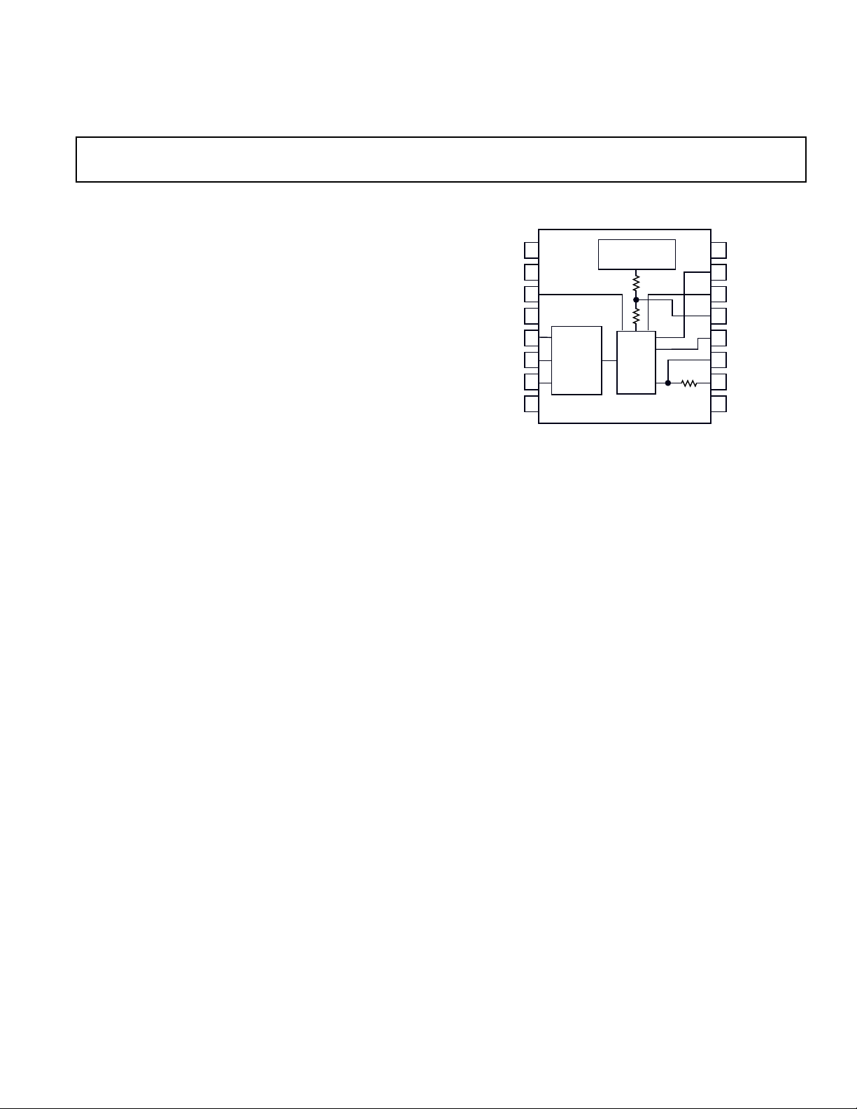
The AD1862 is a monolithic 20-bit digital audio DAC. Each
device provides a 20-bit DAC, 20-bit serial-to-parallel input
register and voltage reference. The digital portion of the
AD1862 is fabricated with CMOS logic elements that are provided by Analog Devices’ BiMOS II process. The analog portion of the AD1862 is fabricated with bipolar and MOS devices
as well as thin-film resistors.
New design, layout and packaging techniques all combine to
produce extremely high performance audio playback. The design of the AD1862 incorporates a digital offset circuit which
improves low-level distortion performance. Low stress packaging techniques are used to minimize stress-induced parametric
shifts. Stress-sensitive circuit elements are located in die areas
which are least affected by packaging stress. Laser-trimming of
initial linearity error affords extremely low total harmonic
distortion. Output glitch is also small, contributing to the overall high level of performance.
The noise performance of the AD1862 is excellent. When used
with the recommended two external noise-reduction capacitors,
it achieves 120 dB signal-to-noise ratio.
The serial input port consists of the clock, data and latch enable
pins. A serial 20-bit, 2s complement data word is clocked into
the DAC, MSB first, by the external data clock. A latch-enable
signal transfers the input word from the internal serial input
20-Bit Audio DAC
AD1862*
FUNCTIONAL BLOCK DIAGRAM
&
VOLTAGE
REFERENCE
20-BIT
DAC
–V
–V
TRIM
+V
CLK
LE
DATA
–V
1
S
2
S
3
4
L
5
INPUT
6
DIGITAL
OFFSET
7
8
L
AD1862
register to the DAC input register. The data clock can function
at 17 MHz, allowing 16 × F
operation. The serial input port is
S
compatible with second-generation digital filter chips for consumer audio products such as the NPC SM5813 and SM5818.
The AD1862 operates with ±5 V to ±12 V supplies for the digital power supplies and ±12 V supplies for the analog supplies.
The digital and analog supplies can be separated for reduced
digital crosstalk. Separate analog and digital common pins are
also provided. The AD1862 typically dissipates less than
300 mW.
The AD1862 is packaged in a 16-pin plastic DIP. The operating
range is guaranteed to be –25°C to +70°C.
PRODUCT HIGHLIGHTS
1. 120 dB signal-to-noise ratio. (typical)
2. 102 dB D-Range performance. (minimum)
3. ±1 dB gain linearity @ –90 dB amplitude.
4. 20-bit resolution provides 120 dB of dynamic range.
5. 16 × F
operation.
S
6. 0.0016% THD+N @ 0 dB signal amplitude. (typical)
7. Space saving 16-pin DIP package.
8. ±1 mA output current.
+V
16
S
15
NR
2
14
ADJ
13
NR
1
12
AGND
11
I
OUT
10
R
F
9
DGND
*Protected by U.S. Patent Numbers: 4,349,811; 4,857,862; 4,855,618;
3,961,326; 4,141,004; 4,902,959.
REV. A
Information furnished by Analog Devices is believed to be accurate and
reliable. However, no responsibility is assumed by Analog Devices for its
use, nor for any infringements of patents or other rights of third parties
which may result from its use. No license is granted by implication or
otherwise under any patent or patent rights of Analog Devices.
One Technology Way, P.O. Box 9106, Norwood, MA 02062-9106, U.S.A.
Tel: 617/329-4700 Fax: 617/326-8703

AD1862–SPECIFICA TIONS
(TA at +258C and 612 V supplies, see Figure 10 for test circuit schematic)
Min Typ Max Units
RESOLUTION 20 Bits
DIGITAL INPUTS V
IH
V
IL
I
@ VIH = 4.0 V 1.0 µA
IH
I
@ VIL = 0.4 V –10 µA
IL
2.0 4.0 V
0.4 0.8 V
Maximum Clock Input Frequency 17 MHz
ACCURACY
Gain Error
Midscale Output Error ±2
TOTAL HARMONIC DISTORTION + NOISE (EIAJ)
1
±
2 %
±
5 µA
0 dB, 990.5 Hz AD1862N-J –98 (0.0012) –96 (0.0016) dB (%)
AD1862N –94 (0.0019) –92 (0.0025) dB (%)
–20 dB, 990.5 Hz AD1862N, N-J –84 (0.0063) –80 (0.01) dB (%)
–60 dB, 990.5 Hz AD1862N, N-J –45 (0.56) –42 (0.8) dB (%)
D-Range, –60 dB, A-Weight Filter 102 dB
SIGNAL-TO-NOISE RATIO
2
: (EIAJ)
1
A-Weight Filter AD1862N-J 113 119 dB
AD1862N 110 119 dB
GAIN LINEARITY
@ –90 dB AD1862N-J ±1dB
AD1862N ±1dB
OUTPUT CURRENT
Bipolar Range ±1mA
Tolerance ±1 62 %
Output Impedance (± 30%) 2.1 kΩ
Settling Time 350 ns
FEEDBACK RESISTOR
Value 3kΩ
Tolerance ±1 62 %
POWER SUPPLY
Voltage V
Voltage V
Current +I, V
and –V
L
and –V
S
L
S
and VS = 12 V, 17 MHz Clock 11 15 mA
L
4.75 12.0 13.2 ±V
10.8 12.0 13.2 ±V
–I, –VL and –VS = –12 V, 17 MHz Clock 13 16 mA
POWER DISSIPATION
VL and VS = 12 V, –VL and –VS = –12 V, 17 MHz Clock 288 372 mW
TEMPERATURE RANGE
Specification +25 °C
Operation –25 +70 °C
Storage –60 +100 °C
NOTES
1
Test Method complies with EIAJ Standard CP-307.
2
The signal-to-noise measurement includes noise contributed by the SE5534A op amp used in the test fixture but does not include the noise contributed by the low
pass filter used in the test fixture.
Specifications in boldface are tested on all production units at final electrical test.
Specifications subject to change without notice.
REV. A–2–

–30
–30
–40
–50
–60
–70
–80
–90
THD N – dB
+
–60dB
0dB
–20dB
–25 0 25 50 75
TEMPERATURE – °C
–40
–50
–60
THD +N – dB
–70
–80
–90
1
FREQUENCY – kHz
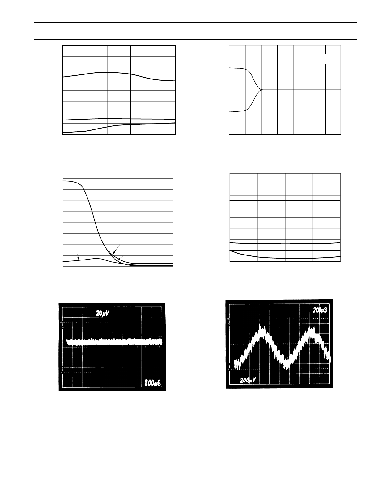
Figure 1. THD+N vs. Frequency
400
350
300
250
Hz
√
200
nV/
150
100
MIDSCALE
50
10
FULLSCALE
–FULLSCALE
–60dB
–20dB
0dB
AD1862
2
AD1862N-J
GAIN LINEARITY
1
–
1
ANALOG OUTPUT ERROR – dB
–
2
–
–
–
–
60
20
DIGITAL INPUT – dB
40
Figure 4. Gain Linearity
0100–80
20
0
1 10 100 1k 10k 100k
Hz
Figure 2. Noise Density
Figure 3. Broadband Noise (20 kHz Bandwidth, Midscale)
Figure 5. THD+N vs. Temperature (1 kHz)
Figure 6. Midscale Differential Linearity
REV. A
–3–

AD1862
WARNING!
ESD SENSITIVE DEVICE
ABSOLUTE MAXIMUM RATINGS*
VL to DGND . . . . . . . . . . . . . . . . . . . . . . . . . . . . 0 to +13.2 V
–V
to DGND . . . . . . . . . . . . . . . . . . . . . . . . . . . . . –VS to 0 V
L
V
to AGND . . . . . . . . . . . . . . . . . . . . . . . . . . . . 0 to +13.2 V
S
–V
to AGND . . . . . . . . . . . . . . . . . . . . . . . . . . . –13.2 to 0 V
S
*Stresses greater than those listed under “Absolute Maximum Ratings” may cause
permanent damage to the device. This is a stress rating only and functional
operation of the device at these or any other conditions above those indicated in the
operational section of this specification is not implied. Exposure to absolute
maximum rating conditions for extended periods may affect device reliability.
AGND to DGND . . . . . . . . . . . . . . . . . . . . . . . –0.3 to +0.3 V
Digital Inputs to DGND . . . . . . . . . . . . . . . . . . . . . –0.3 to V
L
Soldering . . . . . . . . . . . . . . . . . . . . . . . . . . . . . +300°C, 10 sec
Storage Temperature . . . . . . . . . . . . . . . . . . –60°C to +100°C
CAUTION
ESD (electrostatic discharge) sensitive device. Electrostatic charges as high as 4000 V readily
accumulate on the human body and test equipment and can discharge without detection.
Although the AD1862 features proprietary ESD protection circuitry, permanent damage may
occur on devices subjected to high energy electrostatic discharges. Therefore, proper ESD
precautions are recommended to avoid performance degradation or loss of functionality.
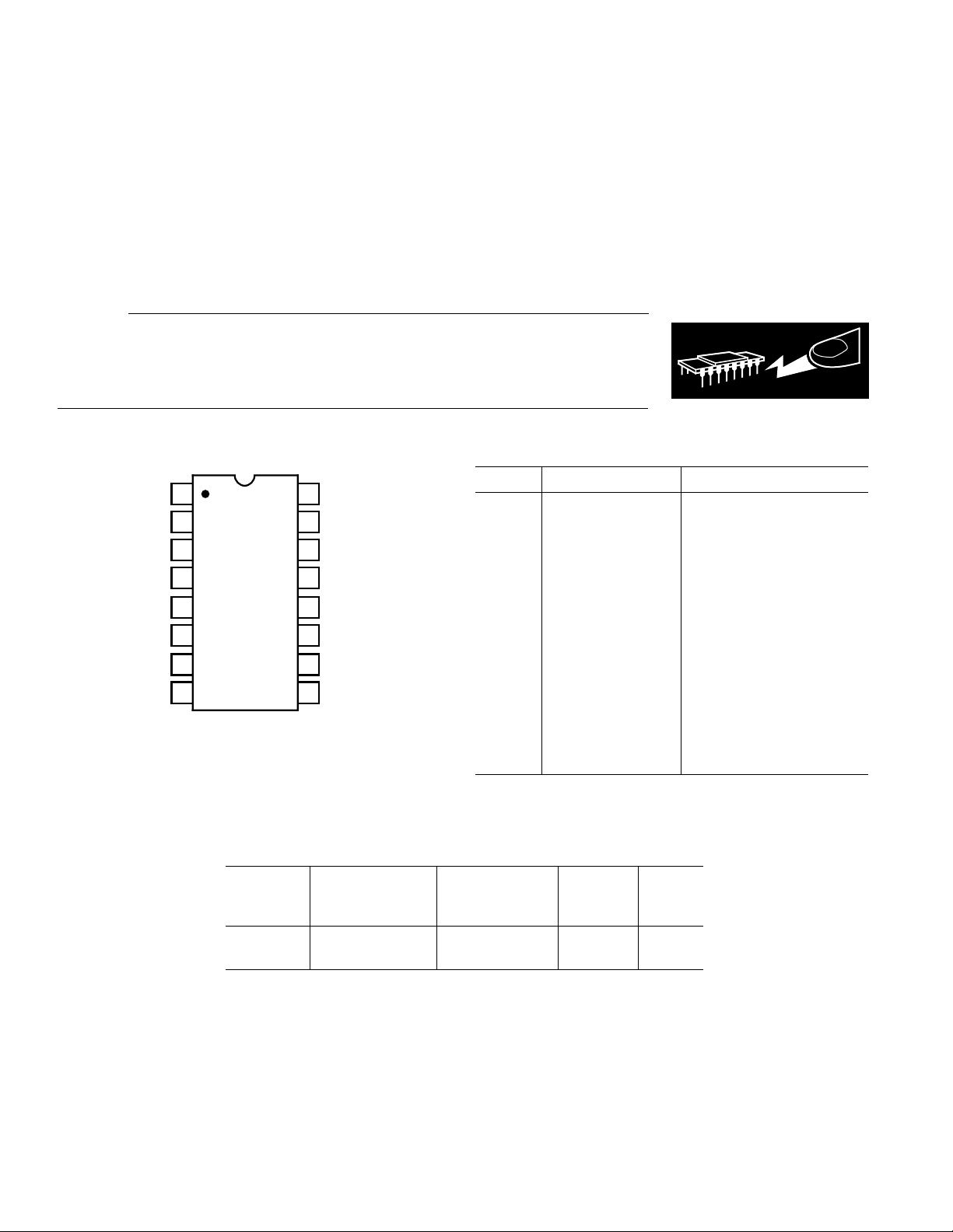
PIN CONFIGURATION PIN DESIGNATIONS
Pin Function Description
–V
–V
TRIM
+V
CLK
LE
DATA
–V
1
S
2
S
3
AD1862
4
L
L
TOP VIEW
(Not to Scale)
5
6
7
89
16
15
14
13
12
11
10
+V
S
NR
2
ADJ
NR
1
AGND
I
OUT
R
F
DGND
11–V
12–V
S
S
13 TRIM Trim Pot Connection
14+V
L
15 CLK External Clock Input
16 LE Latch Enable Input
17 D Data Input
18–V
L
19 DGND Digital Ground
10 R
11 I
F
OUT
12 AGND Analog Ground
13 NR
1
14 ADJ Midscale Adjust
15 NR
16 +V
2
S
Bias Capacitor
Analog Negative Supply
Positive Logic Supply
Negative Logic Supply
Feedback Resistor
Output Current
Reference Capacitor
Bias Capacitor
Positive Analog Supply
ORDERING GUIDE
Operating
Temperature Package
Model Range THD+N @ FS SNR Option*
AD1862N –25°C to +70°C –92 dB, 0.0025% 110 dB N-16
AD1862N-J –25°C to +70°C –96 dB, 0.0016% 113 dB N-16
*N = Plastic DIP.
–4–
REV. A
 Loading...