

1
2
3
4
5
6
7
8
9
LATCH
DAC
SERIAL
INPUT
REGISTER
CONTROL
LOGIC
AD1851/
AD1861
DGND
NC
CLK
LE
DATA
NC = NO CONNECT
TRIM
MSB ADJ
I
OUT
AGND
SJ
R
F
V
OUT
10
11
12
13
14
15
16
NC
+V
S
–V
S
+V
L
I
OUT
a
16-Bit/18-Bit, 16 3 F
PCM Audio DACs
AD1851/AD1861
S
FEATURES
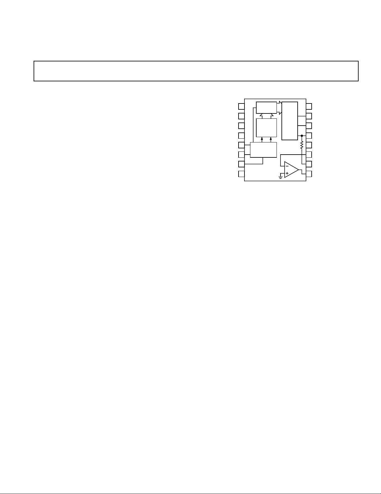
FUNCTIONAL BLOCK DIAGRAM
110 dB SNR
Fast Settling Permits 163 Oversampling
63 V Output
Optional Trim Allows Super-Linear Performance
65 V Operation
16-Pin Plastic DIP and SOIC Packages
Pin-Compatible with AD1856 & AD1860 Audio DACs
2s Complement, Serial Input
APPLICATIONS
High-End Compact Disc Players
Digital Audio Amplifiers
DAT Recorders and Players
Synthesizers and Keyboards
PRODUCT DESCRIPTION
The AD1851/AD1861 is a monolithic PCM audio DAC. The
AD1851 is a 16-bit device, while the AD1861 is an 18-bit device. Each device provides a voltage output amplifier, DAC,
serial-to-parallel register and voltage reference. The digital portion of the AD1851/AD1861 is fabricated with CMOS logic
elements that are provided by Analog Devices’ 2 µm ABCMOS
process. The analog portion of the AD1851/AD1861 is fabricated with bipolar and MOS devices as well as thin-film
resistors.
This combination of circuit elements, as well as careful design
and layout techniques, results in high performance audio playback. Laser-trimming of the linearity error affords low total harmonic distortion. An optional linearity trim pin is provided to
allow residual differential linearity error at midscale to be eliminated. This feature is particularly valuable for low distortion
reproductions of low amplitude signals. Output glitch is also
small, contributing to the overall high level of performance. The
output amplifier achieves fast settling and high slew rates, providing a full ±3 V signal at load currents up to 8 mA. When
used in current output mode, the AD1851/AD1861 provides a
±1 mA output signal. The output amplifier is short circuit
protected and can withstand indefinite shorts to ground.
The serial input interface consists of the clock, data and latch
enable pins. The serial 2s complement data word is clocked into
the DAC, MSB first, by the external clock. The latch enable
signal transfers the input word from the internal serial input
register to the parallel DAC input register. The AD1851 input
clock can support a 12.5 MHz data rate, while the AD1861 input clock can support a 13.5 MHz data rate. This serial input
port is compatible with second generation digital filter chips
used in consumer audio products. These filters operate at oversampling rates of 23, 43, 83 and 163 sampling frequencies.
REV. A
Information furnished by Analog Devices is believed to be accurate and
reliable. However, no responsibility is assumed by Analog Devices for its
use, nor for any infringements of patents or other rights of third parties
which may result from its use. No license is granted by implication or
otherwise under any patent or patent rights of Analog Devices.
The critical specifications of THD+N and signal-to-noise ratio
are 100% tested for all devices.
The AD1851/AD1861 operates with ± 5 V power supplies, making it suitable for home use markets. The digital supply, V
be separated from the analog supplies, V
and –VS, for reduced
S
, can
L
digital crosstalk. Separate analog and digital ground pins are
also provided. Power dissipation is 100 mW typical.
The AD1851/AD1861 is available in either a 16-pin plastic DIP
or a 16-pin plastic SOIC package. Both packages incorporate
the industry standard pinout found on the AD1856 and
AD1860 PCM audio DACs. As a result, the AD1851/AD1861
is a drop-in replacement for designs where ± 5 V supplies have
been used with the AD1856/AD1860. Operation is guaranteed
over the temperature range of –25°C to +70°C and over the
voltage supply range of ±4.75 V to ±5.25 V.
PRODUCT HIGHLIGHTS
l. AD1851 16-bit resolution provides 96 dB dynamic range.
AD1861 18-bit resolution provides 108 dB dynamic range.
2. No external components are required.
3. Operates with ±5 V supplies.
4. Space saving 16-pin SOIC and plastic DIP packages.
5. 100 mW power dissipation.
6. High input clock data rates and 1.5 µs settling time permits
23, 43, 83 and 163 oversampling.
7. ±3 V or ±1 mA output capability.
8. THD + Noise and SNR are 100% tested.
9. Pin-compatible with AD1856 & AD1860 PCM audio DACs.
One Technology Way, P.O. Box 9106, Norwood, MA 02062-9106, U.S.A.
Tel: 617/329-4700 Fax: 617/326-8703
AD1851/AD1861–SPECIFICATIONS
NC = NO CONNECT
1
2
3
4
5
6
7
8 9
10
11
12
13
14
15
16
16-BIT
LATCH
16-BIT
DAC
SERIAL
INPUT
REGISTER
CONTROL
LOGIC
AD1851
DGND
NC
CLK
LE
DATA
TRIM
MSB ADJ
AGND
SJ
NC
–V
S
+V
L
+V
S
I
OUT
R
F
V
OUT
I
OUT
(TA @ +258C and 65 V supplies, unless otherwise noted)
Min Typ Max Units
DIGITAL INPUTS
V
IH
V
IL
I
, VIH = V
IH
L
2.0 +V
0.8 V
1.0 µA
L
V
IIL, VIL = 0.4 –10 µA
ACCURACY
Gain Error ±1%
Midscale Output Voltage ±10 mV
DRIFT (0°C to +70°C)
Total Drift ± 25 ppm of FSR/°C
Bipolar Zero Drift ±4 ppm of FSR/°C
SETTLING TIME (To ±0.0015% of FSR)
Voltage Output
6 V Step 1.5 µs
1 LSB Step 1.0 µs
Slew Rate 9 V/µs
Current Output
1 mA Step 10 Ω to 100 Ω Load 350 ns
1 kΩ Load 350 ns
OUTPUT
Voltage Output Configuration
Bipolar Range 62.88 ±3.0 63.12 V
Output Current ±8mA
Output Impedance 0.1 Ω
Short Circuit Duration Indefinite to Common
Current Output Configuration
Bipolar Range (±30%) ±1.0 mA
Output Impedance (± 30%) 1.7 kΩ
POWER SUPPLY
Voltage
+V
–V
and +V
L
S
S
4.75 5.25 V
–5.25 –4.75 V
TEMPERATURE RANGE
Specification 0 +25 +70 °C
Operation –25 +70 °C
Storage –60 +100 °C
WARM-UP TIME 1 min
Specifications subject to change without notice.
–V
1
S
DGND
2
+V
L
3
NC
4
CLK
5
LE
6
DATA
7
NC
8 9
NC = NO CONNECT
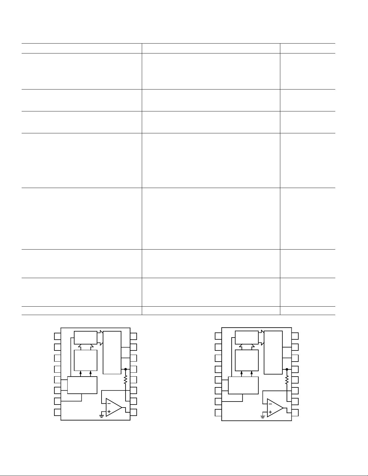
AD1851 Functional Block Diagram
AD1851
16-BIT
LATCH
SERIAL
INPUT
REGISTER
CONTROL
LOGIC
16-BIT
DAC
+V
16
S
TRIM
15
MSB ADJ
14
I
OUT
I
13
OUT
AGND
12
SJ
11
R
10
F
V
OUT
AD1861 Functional Block Diagram
–2–
REV. A
AD1851
AD1851/AD1861
Min Typ Max Units
RESOLUTION 16 Bits
TOTAL HARMONIC DISTORTION + NOISE
0 dB, 990.5 Hz
AD1851N-J, R-J 0.003 0.004 %
AD1851N, R 0.004 0.008 %
–20 dB, 990.5 Hz
AD1851N-J, R-J 0.009 0.016 %
AD1851N, R 0.009 0.040 %
–60 dB, 990.5 Hz
AD1851N-J, R-J 0.9 1.6 %
AD1851N, R 0.9 4.0 %
D-RANGE* (With A-Weight Filter)
–60 dB, 990.5 Hz AD1851N, R 88 dB
AD1851N-J, R-J 96 dB
SIGNAL-TO-NOISE RATIO 107 110 dB
MAXIMUM CLOCK INPUT FREQUENCY 12.5 MHz
ACCURACY
Differential Linearity Error ±0.001 % of FSR
MONOTONICITY 14 Bits
POWER SUPPLY
Current
+I 10.0 13.0 mA
–I –10.0 –15.0 mA
Power Dissipation 100 mW
AD1861
Min Typ Max Units
RESOLUTION 18 Bits
TOTAL HARMONIC DISTORTION + NOISE
0 dB, 990.5 Hz
AD1861N-J, R-J 0.003 0.004 %
AD1861N, R 0.004 0.008 %
–20 dB, 990.5 Hz
AD1861N-J, R-J 0.009 0.016 %
AD1861N, R 0.009 0.040 %
–60 dB, 990.5 Hz
AD1861N-J, R-J 0.9 1.6 %
AD1861N, R 0.9 4.0 %
D-RANGE* (With A-Weight Filter)
–60 dB, 990.5 Hz AD1861N, R 88 dB
AD1861N-J, R-J 96 dB
SIGNAL-TO-NOISE RATIO 107 110 dB
MAXIMUM CLOCK INPUT FREQUENCY 13.5 MHz
ACCURACY
Differential Linearity Error ±0.001 % of FSR
MONOTONICITY 15 Bits
POWER SUPPLY
Current
+I 10.0 13.0 mA
–I –10.0 –15.0 mA
Power Dissipation 100 mW
*Tested in accordance with EIAJ Test Standard CP-307.
Specifications subject to change without notice.
REV. A
–3–
AD1851/AD1861
WARNING!
ESD SENSITIVE DEVICE
ABSOLUTE MAXIMUM RATINGS*
VL to DGND . . . . . . . . . . . . . . . . . . . . . . . . . . . 0 V to 6.50 V
V
to AGND . . . . . . . . . . . . . . . . . . . . . . . . . . . 0 V to 6.50 V
S
–V
to AGND . . . . . . . . . . . . . . . . . . . . . . . . . –6.50 V to 0 V
S
Digital Inputs to DGND . . . . . . . . . . . . . . . . . . . –0.3 V to V
L
AGND to DGND . . . . . . . . . . . . . . . . . . . . . . . . . . . . ±0.3 V
Short Circuit . . . . . . . . . . . . . . . . .Indefinite Short to Ground
Soldering . . . . . . . . . . . . . . . . . . . . . . . . . . . . .+300°C, 10 sec
Storage Temperature . . . . . . . . . . . . . . . . . . –60°C to +100°C
*Stresses greater than those listed under “Absolute Maximum Ratings” may cause
permanent damage to the device. This is a stress rating only and functional
operation of the device at these or any other conditions above those indicated in the
operational section of this specification is not implied. Exposure to absolute
maximum rating conditions for extended periods may affect device reliability.
ORDERING GUIDE
Package
Model Resolution THD + N Option*
AD1851N 16 Bits 0.008% N-16
AD1851N-J 16 Bits 0.004% N-16
AD1851R 16 Bits 0.008% R-16
AD1851R-J 16 Bits 0.004% R-16
AD1861N 18 Bits 0.008% N-16
AD1861N-J 18 Bits 0.004% N-16
AD1861R 18 Bits 0.008% R-16
AD1861R-J 18 Bits 0.004% R-16
*N = Plastic DIP Package; R = Small Outline (SOIC) Package.
PIN DESCRIPTIONS
1–V
S
Analog Negative Power Supply
2 DGND Logic Ground
3V
L
Logic Positive Power Supply
4 NC No Connection
5 CLK Clock Input
6 LE Latch Enable Input
7 DATA Serial Data Input
8 NC No Internal Connection*
9V
10 R
OUT
F
Voltage Output
Feedback Resistor
11 SJ Summing Junction
12 AGND Analog Ground
13 I
OUT
Current Output
14 MSB ADJ MSB Adjustment Terminal
15 TRIM MSB Trimming Potentiometer Terminal
16 V
*Pin 8 has no internal connection; -VL from AD1856 or AD1860 socket can be
safely applied.
S
Analog Positive Power Supply
CAUTION
ESD (electrostatic discharge) sensitive device. The digital control inputs are diode protected;
however, permanent damage may occur on unconnected devices subject to high energy electrostatic fields. Unused devices must be stored in conductive foam or shunts. The protective foam
should be discharged to the destination socket before devices are inserted.
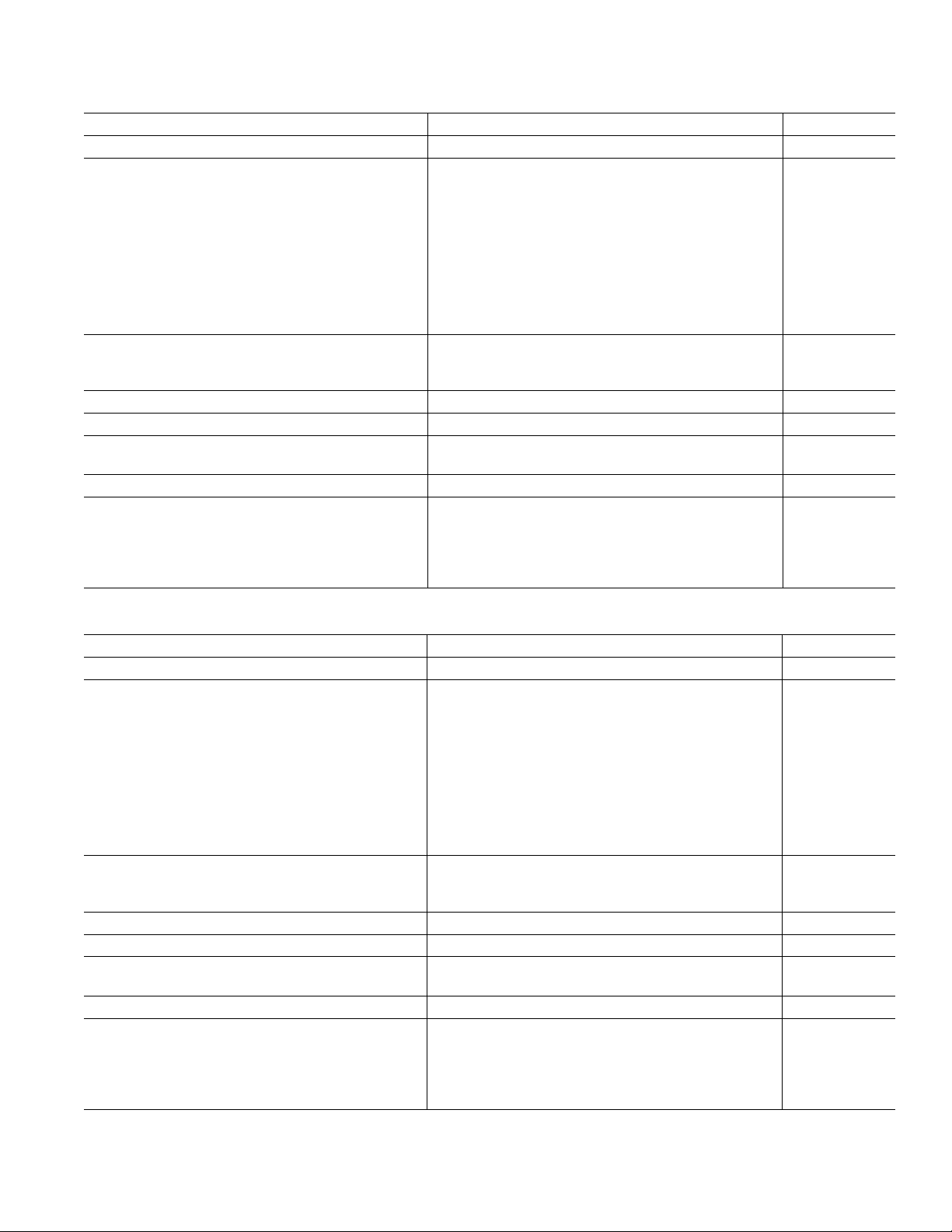
Typical Performance
10
175
150
125
100
PD – mW
75
50
25
2 4 6 8 10 12 14
CLOCK FREQUENCY – MHz
1
0.1
THD+N – %
0.01
0.001
–30 –20 –10 0 10 20 30 40 50 60 70 80 90
TEMPERATURE – °C
–60dB
–20dB
0dB
Power Dissipation vs. Clock Frequency
–4–
THD vs. Temperature
REV. A

TOTAL HARMONIC DISTORTION
REFERENCE
I
OUT
DAC
R
F
AUDIO
OUTPUT
INPUT LATCH
DATALECLOCK
SERIAL-TO-PARALLEL
CONVERSION
Total harmonic distortion plus noise (THD+N) is defined as
the ratio of the square root of the sum of the squares of the values of the first 19 harmonics and noise to the value of the fundamental input frequency. It is usually expressed in percent (%).
THD+N is a measure of the magnitude and distribution of linearity error, differential linearity error, quantization error and
noise. The distribution of these errors may be different, depending on the amplitude of the output signal. Therefore, to be most
useful, THD+N should be specified for both large (0 dB) and
small signal amplitudes (–20 dB and –60 dB).
The THD+N figure of an audio DAC represents the amount of
undesirable signal produced during reconstruction and playback
of an audio waveform. This specification, therefore, provides a
direct method to classify and choose an audio DAC for a
desired level of performance.
SETTLING TIME
Settling time is the time required for the output of the DAC to
reach and remain within a specified error band about its final
value, measured from the digital input transition. It is a primary
measure of dynamic performance.
MIDSCALE ERROR
Midscale error, or bipolar zero error, is the deviation of the actual analog output from the ideal output (0 V) when the 2s
complement input code representing half scale is loaded in the
input register.
D-RANGE DISTORTION
D-range distortion is equal to the value of the total harmonic
distortion + noise (THD+N) plus 60 dB when a signal level of
–60 dB below full scale is reproduced. D-range is tested with a
1 kHz input sine wave. This is measured with a standard Aweight filter as specified by EIAJ Standard CP-307.
SIGNAL-TO-NOISE RATIO
The signal-to-noise ratio (SNR) is defined as the ratio of the
amplitude of the output when a full-scale output is present to
the amplitude of the output with no signal present. This is measured with a standard A-weight filter as specified by EIAJ
Standard CP-307.
AD1851/AD1861
Figure 1. AD1851/AD1861 Functional Block Diagram
FUNCTIONAL DESCRIPTION
The AD1851/AD1861 is a complete monolithic PCM audio
DAC. No additional external components are required for operation. As shown in Figure 1 above, each chip contains a voltage reference, an output amplifier, a DAC, an input latch and a
parallel input register.
The voltage reference consists of a bandgap circuit and buffer
amplifier. This combination of elements produces a reference
voltage that is unaffected by changes in temperature and age.
The DAC output voltage, which is derived from the reference
voltage, is also unaffected by these environmental changes.
The output amplifier uses both MOS and bipolar devices to
produce low offset, high slew rate and optimum settling time.
When combined with the on-chip feedback resistor, the output
op amp converts the output current of the AD1851/AD1861 to
a voltage output.
The DAC uses a combination of segmented decoder and R-2R
architecture to achieve consistent linearity and differential linearity. The resistors which form the ladder structure are fabricated with silicon chromium thin film. Laser-trimming of these
resistors further reduces linearity error, resulting in low output
distortion.
The input register and serial-to-parallel converter are fabricated
with CMOS logic gates. These gates allow the achievement of
fast switching speeds and low power consumption. This contributes to the overall low power dissipation of the AD1851/
AD1861.
REV. A
–5–

AD1851/AD1861
Analog Circuit Considerations
GROUNDING RECOMMENDATIONS
The AD1851/AD1861 has two ground pins, designated Analog
and Digital ground. The analog ground pin is the “high quality”
ground reference point for the device. The analog ground pin
should be connected to the analog common point in the system.
The output load should also be connected to that same point.
The digital ground pin returns ground current from the digital
logic portions of the AD1851/AD1861 circuitry. This pin
should be connected to the digital common point in the system.
As illustrated in Figure 2, the analog and digital grounds should
be connected together at one point in the system.
5V
+
3 16
+V
AD1851/AD1861
DGND AGND
DIGITAL
GROUND
L
–V
S
12 12
5V
–
+5V
+V
S
ANALOG
GROUND
However, three separate voltage supplies are not necessary for
good circuit performance. For example, Figure 3 illustrates a
system where only a single positive and a single negative supply
are available.
In this example, the positive logic and positive analog supplies
must both be connected to +5 V, while the negative analog supply will be connected to –5 V. Performance would benefit from
a measure of isolation between the supplies introduced by using
simple low pass filters in the individual power supply leads.
–V
–5V
+5V
16
+V
S
S
12
12
ANALOG
GROUND
AD1851/AD1861
DGND AGND
DIGITAL
GROUND
+5V
+V
3
L
Figure 3. Alternate Recommended Schematic
As with most linear circuits, changes in the power supplies will
affect the output of the DAC. Analog Devices recommends that
well regulated power supplies with less than 1% ripple be incorporated into the design of any system using the AD1851/AD1861.
Figure 2. Recommended Circuit Schematic
POWER SUPPLIES AND DECOUPLING
The AD1851/AD1861 has three power supply input pins. The
±V
supplies provide the supply voltages to operate the linear
S
portions of the DAC including the voltage reference, output amplifier and control amplifier. The ± V
supplies are designed to
S
operate at ±5 V.
The +V
supply operates the digital portions of the chip includ-
L
ing the input shift register and the input latching circuitry. The
+V
supply is designed to operate at +5 V.
L
Decoupling capacitors should be used on all power supply pins.
Furthermore, good engineering practice suggests that these capacitors be placed as close as possible to the package pins as
well as to the common points. The logic supply, +V
decoupled to digital common, while the analog supplies, ± V
, should be
L
S
,
should be decoupled to analog common.
The use of three separate power supplies will reduce feedthrough
from the digital portion of the system to the linear portion of the
system, thus contributing to improved performance.
OPTIONAL MSB ADJUSTMENT
Use of an optional adjustment circuit allows residual differential
linearity error around midscale to be eliminated. This error is
especially important when low amplitude signals are being reproduced. In those cases, as the signal amplitude decreases, the
ratio of the midscale differential linearity error to the signal amplitude increases, thereby increasing THD.
Therefore, for best performance at low output levels, the optional MSB adjust circuitry shown in Figure 4 may be used to
improve performance. The adjustment should be made with a
small signal input (–20 dB or –60 dB).
TRIM
15
14
MSB
ADJUST
470kΩ 100kΩ 200kΩ
–V
S
1
Figure 4. Optional THD Adjust Circuit
–6–
REV. A

AD1851/AD1861
DATA
CLOCK
LATCH
L
S
B
M
B
S
>40ns
>40ns
>30ns
>30ns
>15ns
>40ns
DATA
CLOCK
LATCH
>15ns
>30ns
>74.1ns
>15ns
AD1851 DIGITAL CIRCUIT CONSIDERATIONS
AD1851 Input Data
Data is transmitted to the AD1851 in a bit stream composed of
16-bit words with a serial, MSB first format. Three signals
must be present to achieve proper operation. They are the
Data, Clock and Latch Enable (LE) signals. Input data bits are
clocked into the input register on the rising edge of the Clock
signal. The LSB is clocked in on the 16th clock pulse. When all
data bits are loaded, a low-going Latch Enable pulse updates
the DAC input. Figure 5 illustrates the general signal requirements for data transfer to the AD1851.
CLOCK
DATA
LATCH
M
S
B
L
S
B
Figure 5. Signal Requirements for AD1851
Figure 6 illustrates the specific timing requirements that must
be met in order for the data transfer to be accomplished properly. The input pins of the AD1851 are both TTL and 5 V
CMOS compatible. The input requirements illustrated in Figures 5 and 6 are compatible with data outputs provided by
popular DSP filter chips used in digital audio playback systems.
The AD1851 input clock can run at a 12.5 MHz rate. This
clock rate will allow data transfer rates for 23, 43 or 83 or
163 oversampling reconstructions.
>30ns
AD1861 DIGITAL CIRCUIT CONSIDERATIONS
AD1861 Input Data
Data is transmitted to the AD1861 in a bit stream composed of
18-bit words with a serial, MSB first format. Three signals
must be present to achieve proper operation. They are the
Data, Clock and Latch Enable (LE) signals. Input data bits are
clocked into the input register on the rising edge of the Clock
signal. The LSB is clocked in on the 18th clock pulse. When all
data bits are loaded, a low-going Latch Enable pulse updates
the DAC input. Figure 7 illustrates the general signal requirements for data transfer to the AD1861.
Figure 7. Signal Requirements for AD1861
Figure 8 illustrates the specific timing requirements that must
be met in order for the data transfer to be accomplished properly. The input pins of the AD1861 are both TTL and 5 V
CMOS compatible. The input requirements illustrated in Figures 7 and 8 are compatible with data outputs provided by
popular DSP filter chips used in digital audio playback systems.
The AD1861 input clock can run at a 13.5 MHz rate. This
clock rate will allow data transfer rates for 23, 43 or 83 or
163 oversampling reconstructions.
DATA
>80.0ns
>40ns
>15ns
>40ns
>30ns
>15ns
>40ns
>15ns
CLOCK
>30ns
LATCH
Figure 6. Timing Relationships of AD1851 Input Signals
Figure 8. Timing Relationships of AD1861 Input Signals
REV. A
–7–

AD1851/AD1861
APPLICATIONS
Figures 9 through 12 show connection diagrams for the
AD1851 and AD1861 and the Yamaha YM3434 and the NPC
SM5813AP/APT digital filter chips.
CLK
+5V
X1 ST 16/18
YM3434
Figure 9. AD1851 with Yamaha YM3434 Digital Filter
+5V
CLK
X1 ST 16/18
YM3434
DLO
BCO
WCO
DRO
DLO
BCO
WCO
CLK
LATCH
DATA
DATA
LATCH
CLK
CLK
LATCH
DATA
AD1851
AD1851
AD1861
OUT
OUT
OUT
LOW
PASS
FILTER
LOW
PASS
FILTER
LOW
PASS
FILTER
LEFT
OUTPUT
RIGHT
OUTPUT
LEFT
OUTPUT
DRO
DATA
LATCH
CLK
AD1861
OUT
LOW
PASS
FILTER
Figure 10. AD1861 with Yamaha YM3434 Digital Filter
RIGHT
OUTPUT
–8–
REV. A

AD1851/AD1861
CLK
X1
COB OW20
SM5813AP/APT
OW18
+5V
Figure 11. AD1851 with NPC SM5813AP/APT Digital Filter
CLK
X1
COB OW20
+5V
+5V
DOL
BCKO
WCKO
DOR
DOL
CLK
LATCH
DATA
DATA
LATCH
CLK
CLK
LATCH
DATA
AD1851
AD1851
AD1861
OUT
OUT
OUT
LOW
PASS
FILTER
LOW
PASS
FILTER
LOW
PASS
FILTER
LEFT
OUTPUT
RIGHT
OUTPUT
LEFT
OUTPUT
SM5813AP/APT
OW18
Figure 12. AD1861 with NPC SM5813AP/APT Digital Filter
BCKO
WCKO
DOR
DATA
LATCH
CLK
AD1861
OUT
LOW
PASS
FILTER
RIGHT
OUTPUT
REV. A
–9–

AD1851/AD1861
2
3
4
5
6
7
89
10
11
12
13
14
15
16
18-BIT
LATCH
18-BIT
DAC
SERIAL
INPUT
REGISTER
CONTROL
LOGIC
AD1860
–V
S
DGND
NC
CLK
LE
DATA
–V
L
+V
L
NC = NO CONNECT
+V
S
TRIM
MSB ADJ
I
OUT
AGND
SJ
R
F
V
OUT
1
I
OUT
1
2
3
4
5
6
7
8
9
10
11
12
TRIM
MSB
I
OUT
AGND
SJ
DR
LR
CK
18-BIT
LATCH
REFERENCE
18-BIT
LATCH
DGND
TRIM
MSB
AGND
SJ
DL
LL
20
13
14
15
16
17
18
19
21
22
23
24
REFERENCE
18-BIT
D/A
18-BIT
D/A
AD1864
+
+
–
–
V
OUT
–V
S
R
F
+V
L
+V
S
I
OUT
R
F
V
OUT
–V
L
OTHER DIGITAL AUDIO COMPONENTS AVAILABLE
FROM ANALOG DEVICES
–V
1
S
DGND
2
+V
3
L
4
NC
5
CLK
6
LE
DATA
7
–V
89
L
16-BIT
LATCH
SERIAL
INPUT
REGISTER
CONTROL
LOGIC
AD1856
16-BIT
DAC
I
OUT
16
15
14
13
12
11
10
+V
S
TRIM
MSB ADJ
I
OUT
AGND
SJ
R
F
V
OUT
NC = NO CONNECT
AD1856 16-BIT AUDIO DAC
Complete, No External Components Required
0.0025% THD
Low Cost
16-Pin DIP or SOIC Package
Standard Pinout
–V
–V
TRIM
+V
CLK
DATA
–V
1
S
2
S
VOLTAGE
REFERENCE
3
4
L
5
INPUT
6
LE
7
8
L
AND
DIGITAL
OFFSET
AD1862
20-BIT
DAC
16
+V
S
15
NR2
14
ADJ
13
NR1
AGND
12
I
11
OUT
R
10
F
DGND
9
AD1860 18-BIT AUDIO DAC
Complete, No External Components Required
0.0025% THD+N
108 dB Signal-to-Noise Ratio
16-Pin DIP or SOIC Package
Standard Pinout
NC = NO CONNECT
AD1862 20-BIT AUDIO DAC
119 dB Signal-to-Noise Ratio
0.0016% THD+N
102 dB D-Range Performance
±1 dB Gain Linearity
16-Pin DIP
–10–
AD1864 DUAL 18-BIT AUDIO DAC
Complete, No External Components
0.0025% THD+N
108 dB Signal-to-Noise Ratio
Cophased Outputs
24-Pin Package
REV. A

OUTLINE DIMENSIONS
Dimensions shown in inches and (mm).
N (Plastic DIP) Package
R (SOIC Surface Mount) Package
AD1851/AD1861
0.299
(7.60)
PIN
1
0.104
(2.650)
16
1
0.050 (1.27)
0.413 (10.50)
0.019
(0.49)
9
8
0.012
(0.30)
0.419
(10.65)
0.013
(0.32)
0.030
(0.75)
0.042
(1.07)
REV. A
–11–

C1458–7–10/90
–12–
PRINTED IN U.S.A.
 Loading...