Analog Devices AD1315KZ Datasheet

High Speed Active Load
a
FEATURES
+50 mA Voltage Programmable Current Range
1.5 ns Propagation Delay
Inhibit Mode Function
High Speed Differential Inputs for Maximum Flexibility
Hermetically Sealed Small Gull Wing Package
Compatible with AD1321, AD1324 Pin Drivers
APPLICATIONS
Automatic Test Equipment
Semiconductor Test System
Board Level Test System
with Inhibit Mode
AD1315
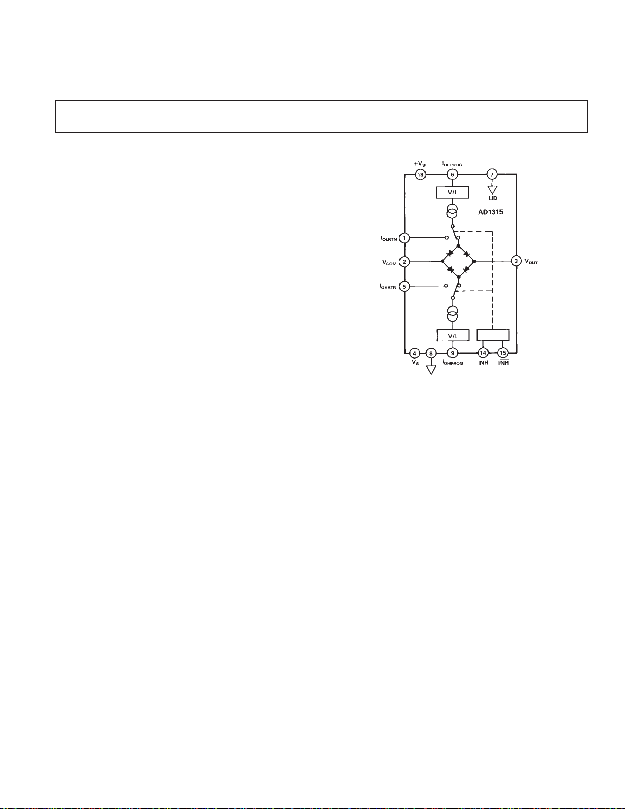
FUNCTIONAL BLOCK DIAGRAM
PRODUCT DESCRIPTION
The AD1315 is a complete, high speed, current switching load
designed for use in linear, digital or mixed signal test systems.
By combining a high speed monolithic process with a unique
surface mount package, this product attains superb electrical
performance while preserving optimum packaging densities in
an ultrasmall 16-lead, hermetically sealed gull wing package.
Featuring current programmability of up to +50 mA, the
AD1315 is designed to force the device under test to source or
sink the programmed I
and IOL currents are determined by applying a corresponding
voltage (5 V = 50 mA) to the I
to-current conversion is performed within the AD1315 thus
allowing the current levels to be set by a standard voltage out
digital-to-analog converter.
The AD1315’s transition from IOH to IOL occurs when the
output voltage of the device under test slews above or below the
programmed threshold, or commutation voltage. The commuta-
OHPROG
and I
and IOL pins. The voltage-
OH
currents. The I
OLPROG
OH
tion voltage is programmable from 2 V to +7 V, covering the
large spectrum of logic devices while able to support the large
current specifications (48 mA) typically associated with line
drivers. To test I/O devices, the active load can be switched into
a high impedance state (Inhibit mode) electrically removing the
active load from the path through the Inhibit mode feature. The
active load leakage current in Inhibit is typically 20 nA.
The Inhibit input circuitry is implemented utilizing high speed
differential inputs with a common-mode voltage range of 7 volts
and a maximum differential voltage of 4 volts. This allows for
the direct interface to the precision of differential ECL timing or
the simplicity of switching the Active Load from a single ended
TTL or CMOS logic source. With switching speeds from IOH
or Io~ into Inhibit of less than 1.5 ns, the AD1315 can be
electrically removed from the signal path “on-the-fly.”
The AD1315 is available in a 16-lead, hermetically sealed gull
wing package and is specified to operate over the ambient commercial temperature range from 0°C to +70°C.
REV. A
Information furnished by Analog Devices is believed to be accurate and
reliable. However, no responsibility is assumed by Analog Devices for its
use, nor for any infringements of patents or other rights of third parties
which may result from its use. No license is granted by implication or
otherwise under any patent or patent rights of Analog Devices.
One Technology Way, P.O. Box 9106, Norwood, MA 02062-9106, U.S.A.
Tel: 617/329-4700 World Wide Web Site: http://www.analog.com
Fax: 617/326-8703 © Analog Devices, Inc., 1997

(All measurements made in free air at +258C. +VS = +10 V, –VS = –5.2 V, unless
AD1315–SPECIFICATIONS
otherwise noted.)
AD1315KZ
Parameter Min Typ Max Units Comments
DIFFERENTIAL INPUT CHARACTERISTICS
INH to INH
Input Voltage, Any One Input –3.0 4.0 Volts
Differential Input Range 0.4 ECL 4.0 Volts
Bias Current –2.0 1.0 2.0 mA
Current Program Voltage Range
I
, 0 mA to +50 mA (Sink)
OH
I
, 0 mA to –50 mA (Source)
OL
Input Resistance 50 kΩ
I
, I
OHRTN
V
OCRTN
, V
COM
I
OH
Range –2.0 +7.0 Volts
DUT
, 0 mA to +50 mA 0.5 +7.0 Volts V
Range
2
IOL, 0 mA to –50 mA –2.0 +4.0 Volts V
OUTPUT CHARACTERISTICS
1
1
0 +5.0 Volts
0 +5.0 Volts
–2.0 +7.0 Volts
– V
DUT
COM
3
– V
COM
DUT
Active (Sink/Source) Mode
Transfer Function 10 mA/V See Figure 1
Accuracy See Figure 1
Linearity Error –0.12 +0.12 % FSR
Gain Error –2.0 +2.0 % FSR
Offset Error –1.0 +1.0 mA
Output Current TC 10 µA/°C
Inhibit Mode
Output Capacitance 3.0 pF
Inhibit Leakage –200 20 200 nA
(t
PD1
PD2
3
4
)
4
)
0.5 1.5 ns
1.5 3.0 ns
DYNAMIC PERFORMANCE
Propagation Delay See Figure 2
±I
to INHIBIT (t
MAX
INHIBIT to ±I
MAX
POWER SUPPLIES
to +VS Difference 15.2 15.4 Volts
–V
S
Supply Range
Positive Supply +9.5 +10 +10.5 Volts
Negative Supply –5.45 –5.2 –4.95 Volts
Current
Positive Supply
Negative Supply
Power Dissipation
7
PSRR
NOTES
1
I
OHPROG/IOLPROG
2
I
OHRTN/IOLRTN
3
V
DUT
4
Measured from the ECL crossing to the 10% change in the output current.
5
I
PROGRAM
6
Maximum power dissipation with +VS = +10 V, –VS = 5.2 V, I
7
For a 1% change in +VS or VS, the output current may change a maximum of 0.05% of Full Scale Range (FSR).
Specifications subject to change without notice.
should be connected to V
= –2 V to +7 V, C
= ±50 mA.
5
5
6
voltage range may be extended to –100 mV due to a possible 1 mA offset current.
= 10 pF, R
TOTAL
to minimize power dissipation.
COM
= 10 Ω. For inhibit leakage tests, V
DUT
PROGRAM
5
+70
5
–100
50 mA, V
+85 +100 mA
–85 –70 mA
1.3 1.54
= 0 V to +5.9 V, IOH = –4 mA, IOL = +4 mA, T
DUT
= V
DUT
= 0 V.
COM
0.05 %/%
CASE
= +36°C.
>1 V
>1 V
–2–
REV. A

AD1315
ABSOLUTE MAXIMUM RATINGS
1
Power Supply Voltage
+V
to GND . . . . . . . . . . . . . . . . . . . . . . . . . . . . . . . +12 V
S
–V
to GND . . . . . . . . . . . . . . . . . . . . . . . . . . . . . . . . –11 V
S
Difference from +V
to –VS . . . . . . . . . . . . . . . . . . . . . 16 V
S
Inputs
Difference from INH to INH . . . . . . . . . . . . . . . . . . . . . 5 V
INH, INH . . . . . . . . . . . . . . . . . . +V
V
, V
COM
I
, IOH Program Voltage . . . . . . . . +VS – 15 V, –VS + 15 V
OL
. . . . . . . . . . . . . . . +VS – 13.1 V, –VS + 13.2 V
DUT
– 13.4 V, –VS + 11 V
S
Operating Temperature Range . . . . . . . . . . . . . . . 0 to +70°C
Storage Temperature Range . . . . . . . . . . . . –65°C to +125°C
Lead Temperature Range (Soldering 20 sec)
2
. . . . . . .+300°C
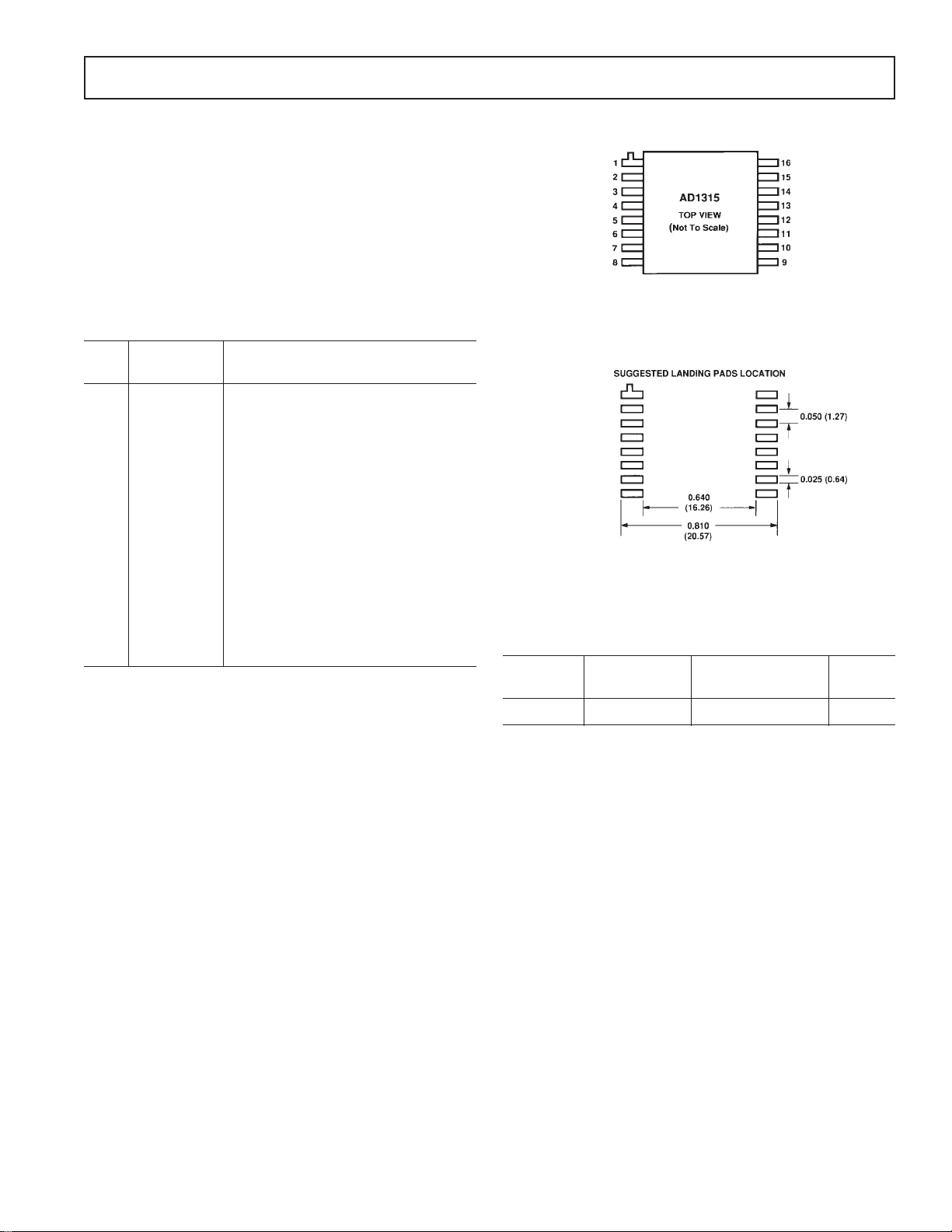
Pin
No. Symbol Function
1I
2V
3V
4–V
5I
6I
OLRTN
COM
DUT
S
OHRTN
OLPROG
Logic Low Current Return
Communication Voltage
Load/Dot Connection
Negative Supply
Logic High Current Return
Logic Low Current Program Voltage
7 LID Lid Connection (Internal)
8 GND Ground
9I
OHPROG
Logic High Current Program Voltage
10 N/C No Connection
11 N/C No Connection
12 N/C No Connection
13 +V
S
Positive Supply
14 INH Inhibit
15 INH Inhibit
16 N/C No Connection
1
Stresses above those listed under Absolute Maximum Ratings may cause permanent damage to the device. This is a stress rating only; functional operation of the
device at these or any other conditions above those indicated in the operational
sections of this specification is not implied. Exposure to absolute maximum rating
conditions for extended periods may affect device reliability.
2
To ensure lead coplanarity (±0.002 inches) and solderability, handling with bare
hands should be avoided and the device should be stored in an environment at
24°C, ±5°C (75°F, ±10°F) with relative humidity not to exceed 65%.
CONNECTION DIAGRAM
SUGGESTED PAD LOCATION
Dimensions shown in inches and (mm).
ORDERING GUIDE
Temperature Package Package
Model Range Description Option*
AD1315KZ 0 to +70°C 16-Lead Gull Wing Z-16B
*Z = Leaded Chip Carrier (Ceramic).
REV. A
–3–
 Loading...