12-Bit 400 MSPS
FEATURES
400 MSPS sample rate
SNR of 63 dBFS @128 MHz
SFDR of 70 dBFS @128 MHz
VSWR of 1:1.5
Wideband ac-coupled input signal conditioning
Enhanced spurious-free dynamic range
Single-ended or differential encode signal
LVDS output levels
Twos complement output data
APPLICATIONS
Communications test equipment
Radar and satellite subsystems
Phased array antennas—digital beam forming
Multichannel, multimode receivers
Secure communications
Wireless and wired broadband communications
Wideband carrier frequency systems
GENERAL DESCRIPTION
The AD12400 is a 12-bit analog-to-digital converter with a
transformer-coupled analog input and digital post processing
for enhanced SFDR. The product operates at a 400 MSPS
conversion rate with outstanding dynamic performance in
wideband carrier systems.
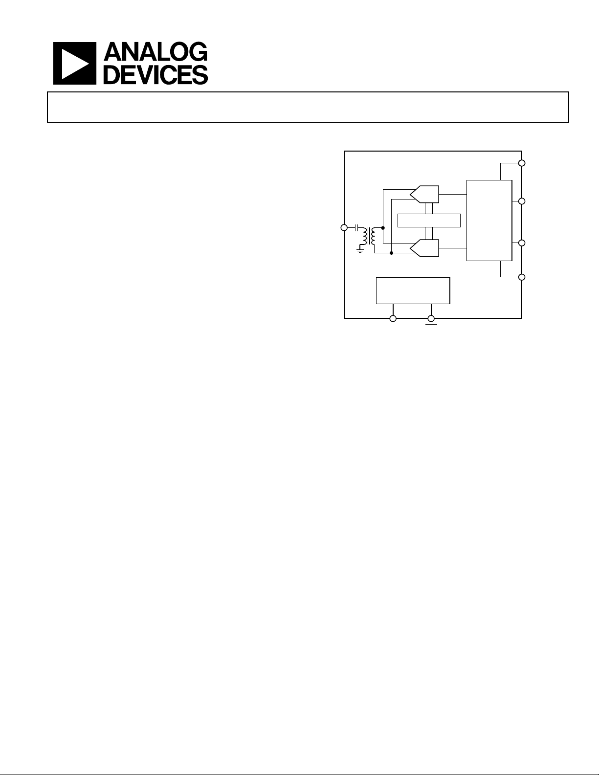
A/D Converter
AD12400
FUNCTIONAL BLOCK DIAGRAM
DATA
AD12400
ADC
A
POST-
A
IN
CLK DISTRIBUTION
ADC
B
CLOCK DISTRIBUTION
DIVIDE BY 2
ENC ENC
Figure 1.
PROCESSING
PRODUCT HIGHLIGHTS
1. Guaranteed sample rate of 400 MSPS.
2. Input signal conditioning with optimized dynamic
performance to 180 MHz.
3. Additional performance options available—contact factory.
READY
A
DA0–DA11
DB0–DB11
DATA
READY
B
03735-0-001
The AD12400 requires 3.8 V analog, 3.3 V digital, and 1.5 V
digital supplies and provides a flexible encode signal that can be
differential or single-ended. No external reference is required.
The AD12400 package style is an enclosed 2.9" × 2.6" × 0.6"
module. Performance is rated over a 0°C to 60°C case
temperature range.
Rev. 0
Information furnished by Analog Devices is believed to be accurate and reliable.
However, no responsibility is assumed by Analog Devices for its use, nor for any
infringements of patents or other rights of third parties that may result from its use.
Specifications subject to change without notice. No license is granted by implication
or otherwise under any patent or patent rights of Analog Devices. Trademarks and
registered trademarks are the property of their respective owners.
4. Proprietary Advanced Filter Bank™ digital post processing
from VCorp® Technologies, Inc.
One Technology Way, P.O. Box 9106, Norwood, MA 02062-9106, U.S.A.
Tel: 781.329.4700 www.analog.com
Fax: 781.326.8703 © 2003 Analog Devices, Inc. All rights reserved.

AD12400
TABLE OF CONTENTS
Specifications..................................................................................... 3
DC Specifications ......................................................................... 3
AC Specifications.......................................................................... 4
Explanation of Test Levels ............................................................... 5
Absolute Maximum Ratings............................................................ 6
ESD Caution.................................................................................. 6
Pin Configuration and Function Descriptions............................. 8
Definitions of Specifications ......................................................... 11
Typical Performance Characteristics ...........................................13
Theory of Operation ...................................................................... 15
Time-Interleaving ADCs ........................................................... 15
Analog Input............................................................................... 16
Clock Input.................................................................................. 16
Digital Outputs ........................................................................... 16
Lead/Lag ...................................................................................... 17
Thermal Considerations............................................................ 17
Package Integrity/Mounting Guidelines ................................. 18
AD12400 Evaluation KIT.......................................................... 19
Power Connector ................................................................... 19
Analog Input........................................................................... 19
Encode ..................................................................................... 19
Data Outputs........................................................................... 19
Adapter Card .......................................................................... 19
Digital Post Processing Control........................................... 19
RESET
...................................................................................... 19
Layout Guidelines........................................................................... 25
PCB Interface.............................................................................. 25
Outline Dimensions....................................................................... 27
Power Supplies ............................................................................ 16
START-UP AND
RESET
........................................................... 17
REVISION HISTORY
Revision 0: Initial Version
Ordering Guide .......................................................................... 27
Rev. 0 | Page 2 of 28

AD12400
SPECIFICATIONS
DC SPECIFICATIONS
Table 1. VA = 3.8 V, VC = 3.3 V, VD = 1.5 V, Encode = 400 MSPS, 0°C ≤ T
AD12400JWS AD12400KWS
Parameter Case Temp Test Level Min Typ Max Min Typ Max Unit
RESOLUTION 12 12 Bits
ACCURACY
No Missing Codes Full IV Guaranteed Guaranteed
Offset Error Full I −12 +12 −12 +12 LSB
Gain Error @ 10 MHz Full I −10 +10 −10 +10 %FS
Differential Nonlinearity
(DNL)
Integral Nonlinearity (INL) 60°C V 0.5 0.5 LSB
TEMPERATURE DRIFT
Gain Error 60°C V 0.02 0.02 %/°C
ANALOG INPUT (AIN)
Full-Scale Input Voltage
Range
Frequency Range Full IV 10 180 10 180 MHz
Flatness (10 MHz-180 MHz) Full IV 0.5 1 0.5 1 dB
Input VSWR (50 Ω )
(10 MHz–180 MHz)
Analog Input Bandwidth 60°C V 450 450 MHz
POWER SUPPLY1
Supply Voltage
VA Full IV 3.6 3.8 3.6 3.8 V
VC Full IV 3.2 3.4 3.2 3.4 V
VD Full IV 1.475 1.575 1.475 1.575 V
Supply Current
IVA (VA = 3.8 V) Full I 0.95 1.11 0.95 1.11 A
IVC (VC = 3.3 V) Full I 400 500 400 500 mA
IVD (VD = 1.5 V) Full I 1.4 1.8 1.4 1.8 A
Total Power Dissipation Full I 7.0 8.5 7.0 8.5 W
ENCODE INPUTS2
Differential Inputs (ENC,
ENC
)
Input Voltage Range Full IV 0.4 0.4 V
Input Resistance 60°C V 100 100 Ω
Input Capacitance 60°C V 4 4 pF
Common-Mode Voltage 60°C V ±3 ±3 V
Single-Ended Inputs (ENC)
Input Voltage Full IV 0.4 2 2.5 0.4 2 2.5 V p-p
Input Resistance 60°C V 50 50 Ω
LOGIC INPUTS (
Logic 1 Voltage Full IV 2.0 2.0 V
Logic 0 Voltage Full IV 0.8 0.8 V
Source IIH 60°C V 10 10 µA
Source IIL 60°C V 1 1 mA
LOGIC OUTPUTS
(DRA, DRB, Output Bits)4
Differential Output Voltage Full IV 247 454 247 454 mV
RESET
)3
60°C V 0.3 0.3 LSB
60°C V 3.2 3.2 V p-p
60°C V 1.5 1.5
≤ 60°C, unless otherwise noted.
CASE
Rev. 0 | Page 3 of 28

AD12400
AD12400JWS AD12400KWS
LOGIC OUTPUTS
Output Drive Current Full IV −4 +4 −4 +4 mA
Output Common-Mode
Voltage
Start-Up Time Full IV 600 600 ms
1
Tested using input frequency of 70 MHz. See Figure 17 for I(VD) variation vs. input frequency.
2
All ac specifications tested by driving ENC single-ended.
3
Refer to Table 5 for logic convention on all logic inputs.
4
Digital Output Logic Levels: DR V = 3.3 V, C
Specifications subject to change without notice.
AC SPECIFICATIONS
Table 2. VA = 3.8 V, VC = 3.3 V, VD = 1.5 V, Encode = 400 MSPS, 0°C ≤ T
AD12400JWS AD12400KWS
Parameter Case Temp Test Level Min Typ Max Min Typ Max Unit
DYNAMIC PERFORMANCE2
SNR
Analog Input 10 MHz Full I 62 64.4 62 64.4 dBFS
@ −1.0 dBFS 70 MHz Full I 61.5 64 61.5 64 dBFS
128 MHz Full I 60 63.5 60 63.5 dBFS
180 MHz Full I 60 62.5 60 62.5 dBFS
SINAD3
Analog Input 10 MHz Full I 61 64 61 64 dBFS
@ −1.0 dBFS 70 MHz Full I 60.5 64 60.5 64 dBFS
128 MHz Full I 59 62.5 59 62.5 dBFS
180 MHz Full I 57 61 57 61 dBFS
Spurious-Free Dynamic Range3
Analog Input 10 MHz Full I 69 80 69 80 dBFS
@ −1.0 dBFS 70 MHz Full I 69 84 69 84 dBFS
128 MHz Full I 67 76 67 76 dBFS
180 MHz Full I 62 71 62 71 dBFS
Image Spur4
Analog Input 10 MHz Full I 60 75 62 75 dBFS
@ −1.0 dBFS 70 MHz Full I 60 72 62 72 dBFS
128 MHz Full I 56 70 62 70 dBFS
180 MHz Full I 54 70 62 70 dBFS
Offset Spur4 60°C V 65 65 dBFS
Analog Input @ −1.0 dBFS
Two-Tone IMD5
F1, F2 @ −6 dBFS 60°C V −75 −75 dBc
SWITCHING SPECIFICATIONS
Conversion Rate6 Full IV 396 400 404 396 400 404 MSPS
Encode Pulsewidth High (tEH)1 60°C V 1.25 1.25 ns
Encode Pulsewidth Low (tEL)1 60°C V 1.25 1.25 ns
DIGITAL OUTPUT PARAMETERS
Valid Time (tV) Full IV 1.9 2.4 3.1 1.9 2.4 3.1 ns
Propagation Delay (tPD) 60°C V 1.20 1.20 ns
Rise Time (tR) (20% to 80%) 60°C V 1 1 ns
Fall Time (tF) (20% to 80%) 60°C V 1 1 ns
Full IV 1.125 1.375 1.125 1.375 V
= 8 pF. 3.3 V LVDS R1 = 100 Ω.
LOAD
1
≤ 60°C, unless otherwise noted.
CASE
Rev. 0 | Page 4 of 28

AD12400
AD12400JWS AD12400KWS
Parameter Case Temp Test Level Min Typ Max Min Typ Max Unit
DR Propagation Delay (t
Data to DR Skew (t
Pipeline Latency7 Full IV 40 40 Cycles
Aperture Delay (tA) 60°C V 1.6 1.6 ns
Aperture Uncertainty (Jitter, tJ) 60°C V 0.4 0.4 ps rms
1
All ac specifications tested with a single-ended 2.0 V p-p ENCODE.
2
Dynamic performance guaranteed for analog input frequencies of 10 MHz to 180 MHz.
3
Not including image spur.
4
Image spur will be at fs/2–A
5
F1 = 70 MHz, F2 = 73 MHz.
6
Parts are tested with 400 MSPS encode. Device can be clocked at lower encode rates, but specifications are not guaranteed. Specifications will be guaranteed by
design for encode 400 MSPS ± 1%.
7
Pipeline latency will be exactly 40 cycles.
EXPLANATION OF TEST LEVELS
I 100% production tested.
II 100% production tested at 25°C and sample tested at specified temperatures.
III Sample tested only.
IV Parameter is guaranteed by design and characterization testing.
V Parameter is a typical value only.
VI
100% production tested at 25°C; guaranteed by design and characterization testing for industrial temperature range; 100%
production tested at temperature extremes for military devices.
) 60°C V 3.88 3.88 ns
EDR
− tPD) 60°C V 2.68 2.68 ns
EDR
and the offset spur will be at fs/2.
IN
Rev. 0 | Page 5 of 28

AD12400
ABSOLUTE MAXIMUM RATINGS
Table 3.
Parameter Value
VA to AGND 5 V
VC to DGND 4 V
VD to DGND 1.65 V
Analog Input Voltage 6 V (DC)
Analog Input Power 18 dBm (AC)
Encode Input Voltage 6 V (DC)
Encode Input Power 12 dBm (AC)
Logic Inputs and Outputs to DGND 5 V
Storage Temperature Range, Ambient −65°C to +150°C
Operating Temperature 0°C to 60°C
ESD CAUTION
ESD (electrostatic discharge) sensitive device. Electrostatic charges as high as 4000 V readily accumulate on
the human body and test equipment and can discharge without detection. Although this product features
proprietary ESD protection circuitry, permanent damage may occur on devices subjected to high energy
electrostatic discharges. Therefore, proper ESD precautions are recommended to avoid performance
degradation or loss of functionality.
Stresses above those listed under Absolute Maximum Ratings
may cause permanent damage to the device. This is a stress
rating only; functional operation of the device at these or any
other conditions above those indicated in the operational
sections of this specification is not implied. Exposure to
absolute maximum rating conditions for extended periods may
affect device reliability.
Rev. 0 | Page 6 of 28

B
AD12400
Table 4. Output Coding (Twos Complement)
Code AIN (V) Digital Output
4095 +1.6 0111 1111 1111
. . .
. . .
. . .
2048 0 0000 0000 0000
2047 −0.000781 1111 1111 1111
. . .
. . .
0 −1.6 1000 0000 0000
Table 5. Option Pin List With Necessary Associated Circuitry
Active
High or
Pin Name
RESET
Low
Low LVTTL High 3.74 kΩ Pull-Up
LEAD/LAG Low LVTTL Low
Logic
Level
Typ e
Default
Level
Associated
Circuitry
Within Part
10 kΩ − 60 kΩ
Pull-Down
3.3V
100Ω
100Ω
100Ω
100Ω
PECL
DRIVER
03735-0-003
ENCODE
ENCODE
3.3V
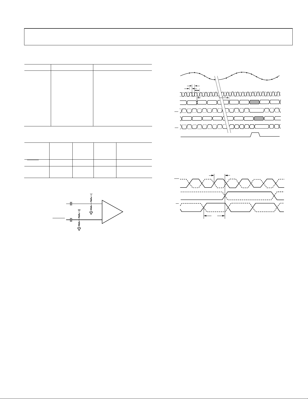
Figure 2. Encode Equivalent Circuit
ENCODE
400MHZ
DATA OUT A
DATA OUT
LEAD LAG
DATA OUT
N– 1
N + 1
N + 2
N + 3
t
EL
t
EH
DRA
DRA
DRB
DRB
*DATA LOST DUE TO ASSERTION OF LEAD/LAG. LATENCY OF 40 ENCODE CLOCK CYCLES BEFORE DATA VALID.
NOTES:
1 IF A SINGLE-ENDED SINEWAVE IS USED FOR ENCODE, USE THE "ZERO CROSSING" POINT (AC-COUPLED) AS THE 50%
POINT AND APPLY THE SAME TIMING INFORMATION.
2 THE LEAD/LAG PIN IS USED TO SYNCHRONIZE THE COLLECTION OF DATA INTO EXTERNAL BUFFER MEMORIES. THE
LEAD/LAG PIN CAN BE APPLIED SYNCHRONOUSLY OR ASYNCHRONOUSLY TO THE AD12400. IF APPLIED
ASYNCHRONOUSLY, LEAD/LAG MUST BE HELD HIGH FOR A MINIMUM OF 5ns TO ENSURE CORRECT OPERATION. THE
FUNCTION WILL SHUT OFF DRA AND DRB UNTIL THE LEAD/LAG PIN IS RELEASED. DRA AND DRB WILL RESUME ON THE
NEXT VALID DRA AFTER LEAD/LAG IS RELEASED.
1/f
S
40 CLOCK CYCLES
N – 40
N – 39
NNN + 2
N + 1
*
N + 4 N + 6 N + 8
*
N + 3 N + 5 N + 7
Figure 3. Timing Diagram
t
ENC
ENC
DR
DR
PD
t
V
Figure 4. Highlighted Timing Diagram
03735-0-002
03735-0-004
Rev. 0 | Page 7 of 28

AD12400
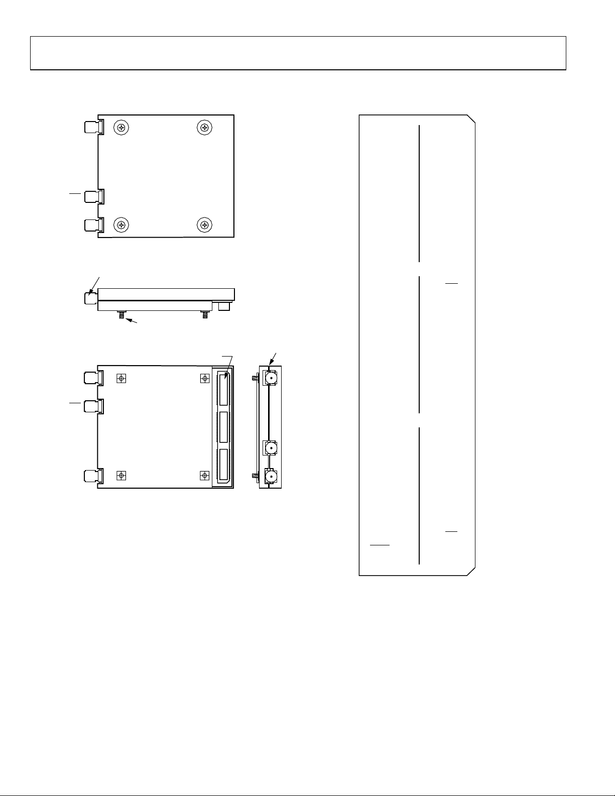
PIN CONFIGURATION AND FUNCTION DESCRIPTIONS
AIN
ENC
ENC
TOP VIEW
JOHNSON SMA-50 OHM CONNECT NO. 142-0711-821
2-56 STUDS 4×
END VIEW
SAMTEC CONNECTOR
QTE-060-01-L-D-A-K-TR
ENC
ENC
AIN
BOTTOM VIEW
NOTES
FOR MATING HALF, USE SAMTEC, INC.
PART NO. QSE-60-01-L-D-A-K.
*INTEGRAL GROUND PLANE CONNECTIONS.
SECTION A = DGND, PINS 121–124.
SECTION B = DGND, PINS 125–128.
SECTION C = AGND, PINS 129–132.
PIN 1
BOARD
LEFT SIDE VIEW
Figure 5. Pin Configuration
PIN 119
PIN 79
PIN 39
PIN 1
VA
VA
VA
VA
AGND
AGND
DNC
DNC
DNC
DNC
DNC
DNC
AGND
AGND
AGND
AGND
AGND
AGND
AGND
AGND
DNC
LEAD/LAG
DA1+
DA1–
DA3+
DA3–
DA5+
DA5–
DA7+
DA7–
DA9+
DA9–
DA11+
DA11–
DNC
DNC
VD
VD
VD
VD
DB1+
DB1–
DB3+
DB3–
DB5+
DB5–
DB7+
DB7–
DB9+
DB9–
DB11+
DB11–
DNC
DNC
DNC
DNC
DNC
RESET
VC
VC
*
VA
VA
VA
VA
AGND
AGND
DNC
DNC
DNC
DNC
DNC
DNC
DNC
AGND
AGND
AGND
AGND
AGND
AGND
AGND
*
DRA
DRA
DA0+
DA0–
DA2+
DA2–
DA4+
DA4–
DA6+
DA6–
DA8+
DA8–
DA10+
DA10–
DNC
PASS
VD
VD
VD
VD
*
DB0+
DB0–
DB2+
DB2–
DB4+
DB4–
DB6+
DB6–
DB8+
DB8–
DB10+
DB10–
DNC
DNC
DRB
DRB
DNC
DNC
VC
VC
PIN 120
C
PIN 80
B
PIN 40
A
PIN 2
03735-0-005
Rev. 0 | Page 8 of 28

AD12400
Table 6. Pin Function Descriptions
Pin Number Mnemonic Function
1, 2, 3, 4 VC Digital Supply, +3.3 V.
5
6−9, 11, 13−16, DNC Do Not Connect.
49, 51−52, 79,
96−108
10
12 DRB Channel B Data Ready. True output.
17 DB11− Channel B Data Bit 11. Complement output bit.
18 DB10− Channel B Data Bit 10. Complement output bit.
19 DB11+ Channel B Data Bit 11. True output bit.
20 DB10+ Channel B Data Bit 10. True output bit.
21 DB9− Channel B Data Bit 9. Complement output bit.
22 DB8− Channel B Data Bit 8. Complement output bit.
23 DB9+ Channel B Data Bit 9. True output bit.
24 DB8+ Channel B Data Bit 8. True output bit.
25 DB7− Channel B Data Bit 7. Complement output bit.
26 DB6− Channel B Data Bit 6. Complement output bit.
27 DB7+ Channel B Data Bit 7. True output bit.
28 DB6+ Channel B Data Bit 6. True output bit.
29 DB5− Channel B Data Bit 5. Complement output bit.
30 DB4− Channel B Data Bit 4. Complement output bit.
31 DB5+ Channel B Data Bit 5. True output bit.
32 DB4+ Channel B Data Bit 4. True output bit.
33 DB3− Channel B Data Bit 3. Complement output bit.
34 DB2− Channel B Data Bit 2. Complement output bit.
35 DB3+ Channel B Data Bit 3. True output bit.
36 DB2+ Channel B Data Bit 2. True output bit.
37 DB1− Channel B Data Bit 1. Complement output bit.
38 DB0− Channel B Data Bit 0. Complement output bit. DB0 is LSB.
39 DB1+ Channel B Data Bit 1. True output bit.
40 DB0+ Channel B Data Bit 0. True output bit. DB0 is LSB.
41−48 VD Digital Supply, +1.5 V.
50 PASS LVTTL. Factory use only. (DNC)
53 DA11− Channel A Data Bit 11. Complement output bit.
54 DA10− Channel A Data Bit 10. Complement output bit.
55 DA11+ Channel A Data Bit 11. True output bit.
56 DA10+ Channel A Data Bit 10. True output bit.
57 DA9− Channel A Data Bit 9. Complement output bit.
58 DA8− Channel A Data Bit 8. Complement output bit.
59 DA9+ Channel A Data Bit 9. True output bit.
60 DA8+ Channel A Data Bit 8. True output bit.
61 DA7− Channel A Data Bit 7. Complement output bit.
62 DA6− Channel A Data Bit 6. Complement output bit.
63 DA7+ Channel A Data Bit 7. True output bit.
64 DA6+ Channel A Data Bit 6. True output bit.
65 DA5− Channel A Data Bit 5. Complement output bit.
66 DA4− Channel A Data Bit 4. Complement output bit.
67 DA5+ Channel A Data Bit 5. True output bit.
RESET
DRB
LVTTL. 0 = Device Reset. Minimum Width = 200 ns. Device resumes operation after 600 ms maximum.
Channel B Data Ready. Complement output.
Rev. 0 | Page 9 of 28
 Loading...