

Page 1

AMD Geode™ SC2200 Processor
Data Book
March 2006
Publication ID: 32580B
AMD Geode™ SC2200 Processor Data Book
Page 2

© 2006 Advanced Micro Devices, Inc. All rights reserved.
The contents of this document are provided in connection with Advanced Micro
Devices, Inc. (“AMD”) products. AMD makes no representations or warranties with
respect to the accuracy or completeness of the contents of this publication and
reserves the right to make changes to specifications and product descriptions at
any time without notice. No license, whether express, implied, arising by estoppel
or otherwise, to any intellectual property rights is granted by this publication.
Except as set forth in AMD’s Standard Terms and Conditions of Sale, AMD
assumes no liability whatsoever, and disclaims any express or implied warranty,
relating to its products including, but not limited to, the implied warranty of merchantability, fitness for a particular purpose, or infringement of any intellectual
property right.
AMD’s products are not designed, intended, authorized or warranted for use as
components in systems intended for surgical implant into the body, or in other
applications intended to support or sustain life, or in any other application in which
the failure of AMD’s product could create a situation where personal injury, death,
or severe property or environmental damage may occur. AMD reserves the right to
discontinue or make changes to its products at any time without notice.
Contacts
www.amd.com
Trademarks
AMD, the AMD Arrow logo, and combinations thereof, and Geode and Virtual System Architecture are
trademarks of Advanced Micro Devices, Inc.
Microsoft and Windows are registered trademarks of Microsoft Corporation in the United States and/or
other jurisdictions.
MMX is a registered trademark of Intel Corporation in the United States and/or other jurisdictions.
Other product names used in this publication are for identification purposes only and may be trademarks
of their respective companies.
2 AMD Geode™ SC2200 Processor Data Book
Page 3

Contents 32580B
Contents
List of Figures . . . . . . . . . . . . . . . . . . . . . . . . . . . . . . . . . . . . . . . . . . . . . . . . . . . . . . . . . . 5
List of Tables . . . . . . . . . . . . . . . . . . . . . . . . . . . . . . . . . . . . . . . . . . . . . . . . . . . . . . . . . . . 9
1.0 Overview . . . . . . . . . . . . . . . . . . . . . . . . . . . . . . . . . . . . . . . . . . . . . . . . . . . . . . . . . 13
1.1 General Description . . . . . . . . . . . . . . . . . . . . . . . . . . . . . . . . . . . . . . . . . . . . . . . . . . . . . . . . . . 13
1.2 Features . . . . . . . . . . . . . . . . . . . . . . . . . . . . . . . . . . . . . . . . . . . . . . . . . . . . . . . . . . . . . . . . . . . 14
2.0 Architecture Overview . . . . . . . . . . . . . . . . . . . . . . . . . . . . . . . . . . . . . . . . . . . . . . 17
2.1 GX1 Module . . . . . . . . . . . . . . . . . . . . . . . . . . . . . . . . . . . . . . . . . . . . . . . . . . . . . . . . . . . . . . . . 17
2.2 Video Processor Module . . . . . . . . . . . . . . . . . . . . . . . . . . . . . . . . . . . . . . . . . . . . . . . . . . . . . . 22
2.3 Core Logic Module . . . . . . . . . . . . . . . . . . . . . . . . . . . . . . . . . . . . . . . . . . . . . . . . . . . . . . . . . . . 23
2.4 SuperI/O Module . . . . . . . . . . . . . . . . . . . . . . . . . . . . . . . . . . . . . . . . . . . . . . . . . . . . . . . . . . . . 23
2.5 Clock, Timers, and Reset Logic . . . . . . . . . . . . . . . . . . . . . . . . . . . . . . . . . . . . . . . . . . . . . . . . . 24
3.0 Signal Definitions . . . . . . . . . . . . . . . . . . . . . . . . . . . . . . . . . . . . . . . . . . . . . . . . . . 25
3.1 Ball Assignments . . . . . . . . . . . . . . . . . . . . . . . . . . . . . . . . . . . . . . . . . . . . . . . . . . . . . . . . . . . . 27
3.2 Strap Options . . . . . . . . . . . . . . . . . . . . . . . . . . . . . . . . . . . . . . . . . . . . . . . . . . . . . . . . . . . . . . . 45
3.3 Multiplexing Configuration . . . . . . . . . . . . . . . . . . . . . . . . . . . . . . . . . . . . . . . . . . . . . . . . . . . . . 46
3.4 Signal Descriptions . . . . . . . . . . . . . . . . . . . . . . . . . . . . . . . . . . . . . . . . . . . . . . . . . . . . . . . . . . 52
4.0 General Configuration Block . . . . . . . . . . . . . . . . . . . . . . . . . . . . . . . . . . . . . . . . 75
4.1 Configuration Block Addresses . . . . . . . . . . . . . . . . . . . . . . . . . . . . . . . . . . . . . . . . . . . . . . . . . 75
4.2 Multiplexing, Interrupt Selection, and Base Address Registers . . . . . . . . . . . . . . . . . . . . . . . . . 76
4.3 WATCHDOG . . . . . . . . . . . . . . . . . . . . . . . . . . . . . . . . . . . . . . . . . . . . . . . . . . . . . . . . . . . . . . . 83
4.4 High-Resolution Timer . . . . . . . . . . . . . . . . . . . . . . . . . . . . . . . . . . . . . . . . . . . . . . . . . . . . . . . . 85
4.5 Clock Generators and PLLs . . . . . . . . . . . . . . . . . . . . . . . . . . . . . . . . . . . . . . . . . . . . . . . . . . . . 87
5.0 SuperI/O Module . . . . . . . . . . . . . . . . . . . . . . . . . . . . . . . . . . . . . . . . . . . . . . . . . . 95
5.1 Features . . . . . . . . . . . . . . . . . . . . . . . . . . . . . . . . . . . . . . . . . . . . . . . . . . . . . . . . . . . . . . . . . . . 96
5.2 Module Architecture . . . . . . . . . . . . . . . . . . . . . . . . . . . . . . . . . . . . . . . . . . . . . . . . . . . . . . . . . . 97
5.3 Configuration Structure/Access . . . . . . . . . . . . . . . . . . . . . . . . . . . . . . . . . . . . . . . . . . . . . . . . . 98
5.4 Standard Configuration Registers . . . . . . . . . . . . . . . . . . . . . . . . . . . . . . . . . . . . . . . . . . . . . . 100
5.5 Real-Time Clock (RTC) . . . . . . . . . . . . . . . . . . . . . . . . . . . . . . . . . . . . . . . . . . . . . . . . . . . . . . 111
5.6 System Wakeup Control (SWC) . . . . . . . . . . . . . . . . . . . . . . . . . . . . . . . . . . . . . . . . . . . . . . . 123
5.7 ACCESS.bus Interface . . . . . . . . . . . . . . . . . . . . . . . . . . . . . . . . . . . . . . . . . . . . . . . . . . . . . . . 128
5.8 Legacy Functional Blocks . . . . . . . . . . . . . . . . . . . . . . . . . . . . . . . . . . . . . . . . . . . . . . . . . . . . 136
AMD Geode™ SC2200 Processor Data Book 3
Page 4

32580B
Contents
6.0 Core Logic Module . . . . . . . . . . . . . . . . . . . . . . . . . . . . . . . . . . . . . . . . . . . . . . . . 149
6.1 Feature List . . . . . . . . . . . . . . . . . . . . . . . . . . . . . . . . . . . . . . . . . . . . . . . . . . . . . . . . . . . . . . . 149
6.2 Module Architecture . . . . . . . . . . . . . . . . . . . . . . . . . . . . . . . . . . . . . . . . . . . . . . . . . . . . . . . . . 150
6.3 Register Descriptions . . . . . . . . . . . . . . . . . . . . . . . . . . . . . . . . . . . . . . . . . . . . . . . . . . . . . . . . 183
6.4 Chipset Register Space . . . . . . . . . . . . . . . . . . . . . . . . . . . . . . . . . . . . . . . . . . . . . . . . . . . . . . 198
7.0 Video Processor Module . . . . . . . . . . . . . . . . . . . . . . . . . . . . . . . . . . . . . . . . . . . 319
7.1 Module Architecture . . . . . . . . . . . . . . . . . . . . . . . . . . . . . . . . . . . . . . . . . . . . . . . . . . . . . . . . . 320
7.2 Functional Description . . . . . . . . . . . . . . . . . . . . . . . . . . . . . . . . . . . . . . . . . . . . . . . . . . . . . . . 321
7.3 Register Descriptions . . . . . . . . . . . . . . . . . . . . . . . . . . . . . . . . . . . . . . . . . . . . . . . . . . . . . . . . 338
8.0 Debugging and Monitoring . . . . . . . . . . . . . . . . . . . . . . . . . . . . . . . . . . . . . . . . . 365
8.1 Testability (JTAG) . . . . . . . . . . . . . . . . . . . . . . . . . . . . . . . . . . . . . . . . . . . . . . . . . . . . . . . . . . . 365
8.2 Engineering Note: Carmel Rev B1 - DFT ACP . . . . . . . . . . . . . . . . . . . . . . . . . . . . . . . . . . . . 366
9.0 Electrical Specifications . . . . . . . . . . . . . . . . . . . . . . . . . . . . . . . . . . . . . . . . . . . 369
9.1 General Specifications . . . . . . . . . . . . . . . . . . . . . . . . . . . . . . . . . . . . . . . . . . . . . . . . . . . . . . . 369
9.2 DC Characteristics . . . . . . . . . . . . . . . . . . . . . . . . . . . . . . . . . . . . . . . . . . . . . . . . . . . . . . . . . . 379
9.3 AC Characteristics . . . . . . . . . . . . . . . . . . . . . . . . . . . . . . . . . . . . . . . . . . . . . . . . . . . . . . . . . . 384
10.0 Package Specifications . . . . . . . . . . . . . . . . . . . . . . . . . . . . . . . . . . . . . . . . . . . . 443
10.1 Thermal Characteristics . . . . . . . . . . . . . . . . . . . . . . . . . . . . . . . . . . . . . . . . . . . . . . . . . . . . . . 443
10.2 Physical Dimensions . . . . . . . . . . . . . . . . . . . . . . . . . . . . . . . . . . . . . . . . . . . . . . . . . . . . . . . . 445
Appendix A Support Documentation . . . . . . . . . . . . . . . . . . . . . . . . . . . . . . . . . . . . 447
A.1 Order Information . . . . . . . . . . . . . . . . . . . . . . . . . . . . . . . . . . . . . . . . . . . . . . . . . . . . . . . . . . 447
A.2 Data Book Revision History . . . . . . . . . . . . . . . . . . . . . . . . . . . . . . . . . . . . . . . . . . . . . . . . . . 448
4 AMD Geode™ SC2200 Processor Data Book
Page 5

List of Figures 32580B
List of Figures
Figure 1-1. Block Diagram . . . . . . . . . . . . . . . . . . . . . . . . . . . . . . . . . . . . . . . . . . . . . . . . . . . . . . . . . . . . 13
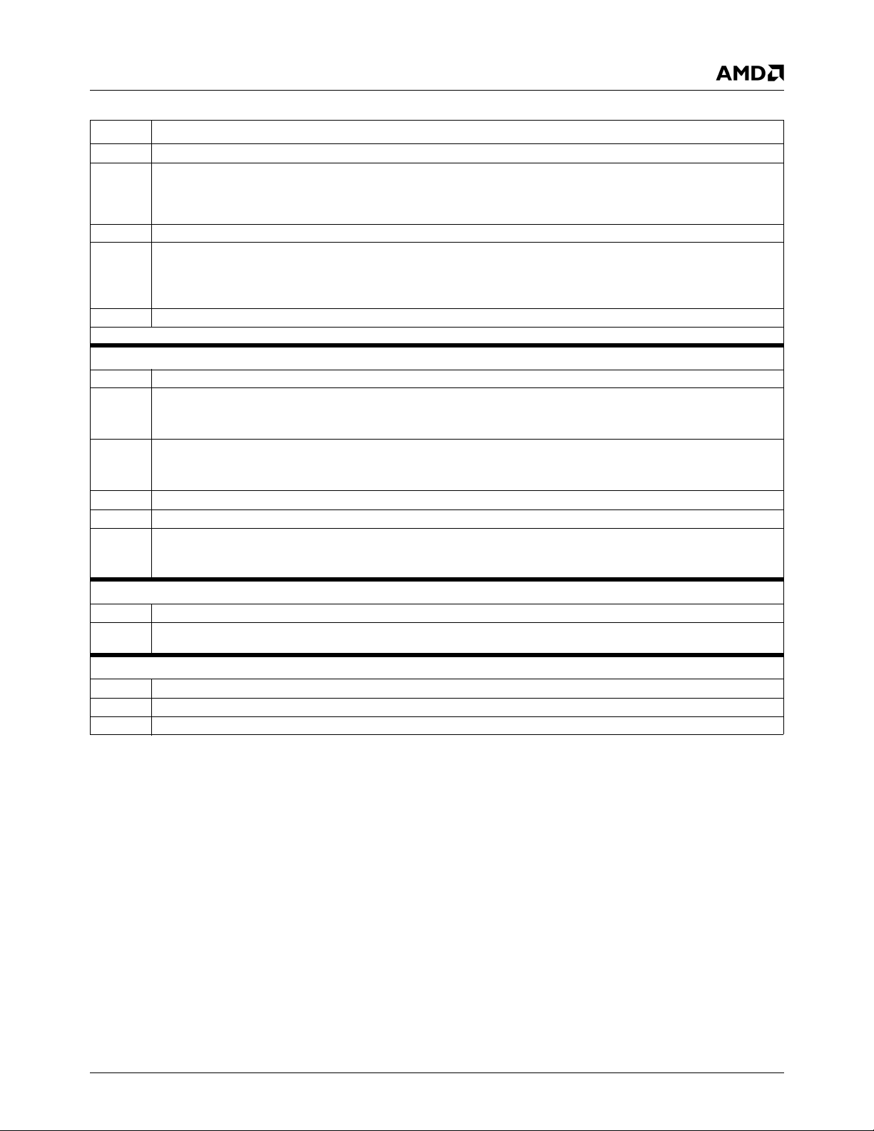
Figure 3-1. Signal Groups . . . . . . . . . . . . . . . . . . . . . . . . . . . . . . . . . . . . . . . . . . . . . . . . . . . . . . . . . . . . 25
Figure 3-2. BGU481 Ball Assignment Diagram . . . . . . . . . . . . . . . . . . . . . . . . . . . . . . . . . . . . . . . . . . . . 28
Figure 4-1. WATCHDOG Block Diagram . . . . . . . . . . . . . . . . . . . . . . . . . . . . . . . . . . . . . . . . . . . . . . . . . 83
Figure 4-2. Clock Generation Block Diagram . . . . . . . . . . . . . . . . . . . . . . . . . . . . . . . . . . . . . . . . . . . . . . 87
Figure 4-3. Recommended Oscillator External Circuitry . . . . . . . . . . . . . . . . . . . . . . . . . . . . . . . . . . . . . 88
Figure 4-4. PLL3 and Dividers Block Diagram . . . . . . . . . . . . . . . . . . . . . . . . . . . . . . . . . . . . . . . . . . . . . 91
Figure 5-1. SIO Block Diagram . . . . . . . . . . . . . . . . . . . . . . . . . . . . . . . . . . . . . . . . . . . . . . . . . . . . . . . . 95
Figure 5-2. Detailed SIO Block Diagram . . . . . . . . . . . . . . . . . . . . . . . . . . . . . . . . . . . . . . . . . . . . . . . . . 97
Figure 5-3. Structure of the Standard Configuration Register File . . . . . . . . . . . . . . . . . . . . . . . . . . . . . . 98
Figure 5-4. Standard Configuration Registers Map . . . . . . . . . . . . . . . . . . . . . . . . . . . . . . . . . . . . . . . . 100
Figure 5-5. Recommended Oscillator External Circuitry . . . . . . . . . . . . . . . . . . . . . . . . . . . . . . . . . . . . 111
Figure 5-6. External Oscillator Connections . . . . . . . . . . . . . . . . . . . . . . . . . . . . . . . . . . . . . . . . . . . . . . 112
Figure 5-7. Divider Chain Control . . . . . . . . . . . . . . . . . . . . . . . . . . . . . . . . . . . . . . . . . . . . . . . . . . . . . . 112
Figure 5-8. Power Supply Connections . . . . . . . . . . . . . . . . . . . . . . . . . . . . . . . . . . . . . . . . . . . . . . . . . 114
Figure 5-9. Typical Battery Configuration . . . . . . . . . . . . . . . . . . . . . . . . . . . . . . . . . . . . . . . . . . . . . . . . 114
Figure 5-10. Typical Battery Current: Battery Backed Power Mode @ T
Figure 5-11. Typical Battery Current: Normal Operation Mode . . . . . . . . . . . . . . . . . . . . . . . . . . . . . . . . 114
Figure 5-12. Interrupt/Status Timing . . . . . . . . . . . . . . . . . . . . . . . . . . . . . . . . . . . . . . . . . . . . . . . . . . . . . 116
Figure 5-13. Bit Transfer . . . . . . . . . . . . . . . . . . . . . . . . . . . . . . . . . . . . . . . . . . . . . . . . . . . . . . . . . . . . . 128
Figure 5-14. Start and Stop Conditions . . . . . . . . . . . . . . . . . . . . . . . . . . . . . . . . . . . . . . . . . . . . . . . . . . 128
Figure 5-15. ACCESS.bus Data Transaction . . . . . . . . . . . . . . . . . . . . . . . . . . . . . . . . . . . . . . . . . . . . . . 129
Figure 5-16. ACCESS.bus Acknowledge Cycle . . . . . . . . . . . . . . . . . . . . . . . . . . . . . . . . . . . . . . . . . . . . 129
Figure 5-17. A Complete ACCESS.bus Data Transaction . . . . . . . . . . . . . . . . . . . . . . . . . . . . . . . . . . . . 130
Figure 5-18. UART Mode Register Bank Architecture . . . . . . . . . . . . . . . . . . . . . . . . . . . . . . . . . . . . . . . 138
Figure 5-19. IRCP/SP3 Register Bank Architecture . . . . . . . . . . . . . . . . . . . . . . . . . . . . . . . . . . . . . . . . . 142
Figure 6-1. Core Logic Module Block Diagram . . . . . . . . . . . . . . . . . . . . . . . . . . . . . . . . . . . . . . . . . . . 150
Figure 6-2. Non-Posted Fast-PCI to ISA Access . . . . . . . . . . . . . . . . . . . . . . . . . . . . . . . . . . . . . . . . . . 156
Figure 6-3. PCI to ISA Cycles with Delayed Transaction Enabled . . . . . . . . . . . . . . . . . . . . . . . . . . . . . 157
Figure 6-4. ISA DMA Read from PCI Memory . . . . . . . . . . . . . . . . . . . . . . . . . . . . . . . . . . . . . . . . . . . . 158
Figure 6-5. ISA DMA Write to PCI Memory . . . . . . . . . . . . . . . . . . . . . . . . . . . . . . . . . . . . . . . . . . . . . . 158
Figure 6-6. PCI Change to Sub-ISA and Back . . . . . . . . . . . . . . . . . . . . . . . . . . . . . . . . . . . . . . . . . . . . 160
Figure 6-7. PIT Timer . . . . . . . . . . . . . . . . . . . . . . . . . . . . . . . . . . . . . . . . . . . . . . . . . . . . . . . . . . . . . . . 162
Figure 6-8. PIC Interrupt Controllers . . . . . . . . . . . . . . . . . . . . . . . . . . . . . . . . . . . . . . . . . . . . . . . . . . . 163
Figure 6-9. PCI and IRQ Interrupt Mapping . . . . . . . . . . . . . . . . . . . . . . . . . . . . . . . . . . . . . . . . . . . . . . 164
Figure 6-10. SMI Generation for NMI . . . . . . . . . . . . . . . . . . . . . . . . . . . . . . . . . . . . . . . . . . . . . . . . . . . . 165
Figure 6-11. General Purpose Timer and UDEF Trap SMI Tree Example . . . . . . . . . . . . . . . . . . . . . . . . 173
Figure 6-12. PRD Table Example . . . . . . . . . . . . . . . . . . . . . . . . . . . . . . . . . . . . . . . . . . . . . . . . . . . . . . 177
Figure 6-13. AC97 V2.0 Codec Signal Connections . . . . . . . . . . . . . . . . . . . . . . . . . . . . . . . . . . . . . . . . 178
Figure 6-14. Audio SMI Tree Example . . . . . . . . . . . . . . . . . . . . . . . . . . . . . . . . . . . . . . . . . . . . . . . . . . . 180
Figure 6-15. Typical Setup . . . . . . . . . . . . . . . . . . . . . . . . . . . . . . . . . . . . . . . . . . . . . . . . . . . . . . . . . . . . 181
Figure 7-1. Video Processor Block Diagram . . . . . . . . . . . . . . . . . . . . . . . . . . . . . . . . . . . . . . . . . . . . . 320
Figure 7-2. NTSC 525 Lines, 60 Hz, Odd Field . . . . . . . . . . . . . . . . . . . . . . . . . . . . . . . . . . . . . . . . . . . 322
Figure 7-3. NTSC 525 Lines, 60 Hz, Even Field . . . . . . . . . . . . . . . . . . . . . . . . . . . . . . . . . . . . . . . . . . 322
Figure 7-4. VIP Block Diagram . . . . . . . . . . . . . . . . . . . . . . . . . . . . . . . . . . . . . . . . . . . . . . . . . . . . . . . . 323
= 25°C . . . . . . . . . . . . . . . . . 114
C
AMD Geode™ SC2200 Processor Data Book 5
Page 6

32580B
List of Figures
Figure 7-5. Capture Video Mode Bob Example Using One Video Frame Buffer . . . . . . . . . . . . . . . . . . 325
Figure 7-6. Capture Video Mode Weave Example Using Two Video Frame Buffers . . . . . . . . . . . . . . . 326
Figure 7-7. Video Block Diagram . . . . . . . . . . . . . . . . . . . . . . . . . . . . . . . . . . . . . . . . . . . . . . . . . . . . . . 327
Figure 7-8. Horizontal Downscaler Block Diagram . . . . . . . . . . . . . . . . . . . . . . . . . . . . . . . . . . . . . . . . . 328
Figure 7-9. Linear Interpolation Calculation . . . . . . . . . . . . . . . . . . . . . . . . . . . . . . . . . . . . . . . . . . . . . . 329
Figure 7-10. Mixer/Blender Block Diagram . . . . . . . . . . . . . . . . . . . . . . . . . . . . . . . . . . . . . . . . . . . . . . . 330
Figure 7-11. Graphics/Video Frame with Alpha Windows . . . . . . . . . . . . . . . . . . . . . . . . . . . . . . . . . . . . 332
Figure 7-12. Color Key and Alpha Blending Logic . . . . . . . . . . . . . . . . . . . . . . . . . . . . . . . . . . . . . . . . . . 334
Figure 7-13. DAC Voltage Levels . . . . . . . . . . . . . . . . . . . . . . . . . . . . . . . . . . . . . . . . . . . . . . . . . . . . . . . 335
Figure 7-14. TFT Power Sequence . . . . . . . . . . . . . . . . . . . . . . . . . . . . . . . . . . . . . . . . . . . . . . . . . . . . . 336
Figure 7-15. PLL Block Diagram . . . . . . . . . . . . . . . . . . . . . . . . . . . . . . . . . . . . . . . . . . . . . . . . . . . . . . . 337
Figure 9-1. Differential Input Sensitivity for Common Mode Range . . . . . . . . . . . . . . . . . . . . . . . . . . . . 382
Figure 9-2. General Drive level and Measurement Points . . . . . . . . . . . . . . . . . . . . . . . . . . . . . . . . . . . 384
Figure 9-3. Drive Level and Measurement Points . . . . . . . . . . . . . . . . . . . . . . . . . . . . . . . . . . . . . . . . . 385
Figure 9-4. Memory Controller Output Valid Timing Diagram . . . . . . . . . . . . . . . . . . . . . . . . . . . . . . . . 387
Figure 9-5. Read Data In Setup and Hold Timing Diagram . . . . . . . . . . . . . . . . . . . . . . . . . . . . . . . . . . 387
Figure 9-6. Video Input Port Timing Diagram . . . . . . . . . . . . . . . . . . . . . . . . . . . . . . . . . . . . . . . . . . . . . 388
Figure 9-7. TFT Timing Diagram . . . . . . . . . . . . . . . . . . . . . . . . . . . . . . . . . . . . . . . . . . . . . . . . . . . . . . 389
Figure 9-8. ACB Signals: Rising Time and Falling Timing Diagram . . . . . . . . . . . . . . . . . . . . . . . . . . . . 392
Figure 9-9. ACB Start and Stop Condition Timing Diagram . . . . . . . . . . . . . . . . . . . . . . . . . . . . . . . . . . 392
Figure 9-10. ACB Start Condition Timing Diagram . . . . . . . . . . . . . . . . . . . . . . . . . . . . . . . . . . . . . . . . . 393
Figure 9-11. ACB Data Bit Timing Diagram . . . . . . . . . . . . . . . . . . . . . . . . . . . . . . . . . . . . . . . . . . . . . . . 393
Figure 9-12. Testing Setup for Slew Rate and Minimum Timing . . . . . . . . . . . . . . . . . . . . . . . . . . . . . . . 394
Figure 9-13. V/I Curves for PCI Output Signals . . . . . . . . . . . . . . . . . . . . . . . . . . . . . . . . . . . . . . . . . . . . 395
Figure 9-14. PCICLK Timing and Measurement Points . . . . . . . . . . . . . . . . . . . . . . . . . . . . . . . . . . . . . . 396
Figure 9-15. Load Circuits for Maximum Time Measurements . . . . . . . . . . . . . . . . . . . . . . . . . . . . . . . . 397
Figure 9-16. Output Timing Measurement Conditions . . . . . . . . . . . . . . . . . . . . . . . . . . . . . . . . . . . . . . . 398
Figure 9-17. Input Timing Measurement Conditions . . . . . . . . . . . . . . . . . . . . . . . . . . . . . . . . . . . . . . . . 399
Figure 9-18. PCI Reset Timing . . . . . . . . . . . . . . . . . . . . . . . . . . . . . . . . . . . . . . . . . . . . . . . . . . . . . . . . . 399
Figure 9-19. Sub-ISA Read Operation Timing Diagram . . . . . . . . . . . . . . . . . . . . . . . . . . . . . . . . . . . . . . 402
Figure 9-20. Sub-ISA Write Operation Timing Diagram . . . . . . . . . . . . . . . . . . . . . . . . . . . . . . . . . . . . . . 403
Figure 9-21. LPC Output Timing Diagram . . . . . . . . . . . . . . . . . . . . . . . . . . . . . . . . . . . . . . . . . . . . . . . . 404
Figure 9-22. LPC Input Timing Diagram . . . . . . . . . . . . . . . . . . . . . . . . . . . . . . . . . . . . . . . . . . . . . . . . . . 404
Figure 9-23. IDE Reset Timing Diagram . . . . . . . . . . . . . . . . . . . . . . . . . . . . . . . . . . . . . . . . . . . . . . . . . 405
Figure 9-24. Register Transfer to/from Device Timing Diagram . . . . . . . . . . . . . . . . . . . . . . . . . . . . . . . . 407
Figure 9-25. PIO Data Transfer to/from Device Timing Diagram . . . . . . . . . . . . . . . . . . . . . . . . . . . . . . . 409
Figure 9-26. Multiword DMA Data Transfer Timing Diagram . . . . . . . . . . . . . . . . . . . . . . . . . . . . . . . . . . 411
Figure 9-27. Initiating an UltraDMA Data in Burst Timing Diagram . . . . . . . . . . . . . . . . . . . . . . . . . . . . . 413
Figure 9-28. Sustained UltraDMA Data In Burst Timing Diagram . . . . . . . . . . . . . . . . . . . . . . . . . . . . . . 414
Figure 9-29. Host Pausing an UltraDMA Data In Burst Timing Diagram . . . . . . . . . . . . . . . . . . . . . . . . . 415
Figure 9-30. Device Terminating an UltraDMA Data In Burst Timing Diagram . . . . . . . . . . . . . . . . . . . . 416
Figure 9-31. Host Terminating an UltraDMA Data In Burst Timing Diagram . . . . . . . . . . . . . . . . . . . . . . 417
Figure 9-32. Initiating an UltraDMA Data Out Burst Timing Diagram . . . . . . . . . . . . . . . . . . . . . . . . . . . . 418
Figure 9-33. Sustained UltraDMA Data Out Burst Timing Diagram . . . . . . . . . . . . . . . . . . . . . . . . . . . . . 419
Figure 9-34. Device Pausing an UltraDMA Data Out Burst Timing Diagram . . . . . . . . . . . . . . . . . . . . . . 420
Figure 9-35. Host Terminating an UltraDMA Data Out Burst Timing Diagram . . . . . . . . . . . . . . . . . . . . . 421
Figure 9-36. Device Terminating an UltraDMA Data Out Burst Timing Diagram . . . . . . . . . . . . . . . . . . . 422
Figure 9-37. Data Signal Rise and Fall Timing Diagram . . . . . . . . . . . . . . . . . . . . . . . . . . . . . . . . . . . . . 425
Figure 9-38. Source Differential Data Jitter Timing Diagram . . . . . . . . . . . . . . . . . . . . . . . . . . . . . . . . . . 425
Figure 9-39. EOP Width Timing Diagram . . . . . . . . . . . . . . . . . . . . . . . . . . . . . . . . . . . . . . . . . . . . . . . . . 426
Figure 9-40. Receiver Jitter Tolerance Timing Diagram . . . . . . . . . . . . . . . . . . . . . . . . . . . . . . . . . . . . . . 426
Figure 9-41. UART, Sharp-IR, SIR, and Consumer Remote Control Timing Diagram . . . . . . . . . . . . . . . 427
Figure 9-42. Fast IR (MIR and FIR) Timing Diagram . . . . . . . . . . . . . . . . . . . . . . . . . . . . . . . . . . . . . . . . 428
Figure 9-43. Standard Parallel Port Typical Data Exchange Timing Diagram . . . . . . . . . . . . . . . . . . . . . 429
Figure 9-44. Enhanced Parallel Port Timing Diagram . . . . . . . . . . . . . . . . . . . . . . . . . . . . . . . . . . . . . . . 430
6 AMD Geode™ SC2200 Processor Data Book
Page 7

List of Figures
32580B
Figure 9-45. ECP Forward Mode Timing Diagram . . . . . . . . . . . . . . . . . . . . . . . . . . . . . . . . . . . . . . . . . . 431
Figure 9-46. ECP Reverse Mode Timing Diagram . . . . . . . . . . . . . . . . . . . . . . . . . . . . . . . . . . . . . . . . . . 432
Figure 9-47. AC97 Reset Timing Diagram . . . . . . . . . . . . . . . . . . . . . . . . . . . . . . . . . . . . . . . . . . . . . . . . 433
Figure 9-48. AC97 Sync Timing Diagram . . . . . . . . . . . . . . . . . . . . . . . . . . . . . . . . . . . . . . . . . . . . . . . . . 433
Figure 9-49. AC97 Clocks Diagram . . . . . . . . . . . . . . . . . . . . . . . . . . . . . . . . . . . . . . . . . . . . . . . . . . . . . 434
Figure 9-50. AC97 Data TIming Diagram . . . . . . . . . . . . . . . . . . . . . . . . . . . . . . . . . . . . . . . . . . . . . . . . . 435
Figure 9-51. AC97 Rise and Fall Timing Diagram . . . . . . . . . . . . . . . . . . . . . . . . . . . . . . . . . . . . . . . . . . 436
Figure 9-52. AC97 Low Power Mode Timing Diagram . . . . . . . . . . . . . . . . . . . . . . . . . . . . . . . . . . . . . . . 437
Figure 9-53. PWRBTN# Trigger and ONCTL# Timing Diagram . . . . . . . . . . . . . . . . . . . . . . . . . . . . . . . 438
Figure 9-54. GPWIO and ONCTL# Timing Diagram . . . . . . . . . . . . . . . . . . . . . . . . . . . . . . . . . . . . . . . . 438
Figure 9-55. Power-Up Sequencing With PWRBTN# Timing Diagram . . . . . . . . . . . . . . . . . . . . . . . . . . 439
Figure 9-56. Power-Up Sequencing Without PWRBTN# Timing Diagram . . . . . . . . . . . . . . . . . . . . . . . . 440
Figure 9-57. TCK Measurement Points and Timing Diagram . . . . . . . . . . . . . . . . . . . . . . . . . . . . . . . . . 441
Figure 9-58. JTAG Test Timing Diagram . . . . . . . . . . . . . . . . . . . . . . . . . . . . . . . . . . . . . . . . . . . . . . . . . 442
Figure 10-1. Heatsink Example . . . . . . . . . . . . . . . . . . . . . . . . . . . . . . . . . . . . . . . . . . . . . . . . . . . . . . . . 444
Figure 10-2. BGU481 Package - Top View . . . . . . . . . . . . . . . . . . . . . . . . . . . . . . . . . . . . . . . . . . . . . . . 445
Figure 10-3. BGU481 Package - Bottom View . . . . . . . . . . . . . . . . . . . . . . . . . . . . . . . . . . . . . . . . . . . . . 446
AMD Geode™ SC2200 Processor Data Book 7
Page 8

32580B
List of Figures
8 AMD Geode™ SC2200 Processor Data Book
Page 9

List of Tables 32580B
List of Tables
Table 2-1. SC2200 Memory Controller Register Summary . . . . . . . . . . . . . . . . . . . . . . . . . . . . . . . . . . . 18
Table 2-2. SC2200 Memory Controller Registers . . . . . . . . . . . . . . . . . . . . . . . . . . . . . . . . . . . . . . . . . .18
Table 3-1. Signal Definitions Legend . . . . . . . . . . . . . . . . . . . . . . . . . . . . . . . . . . . . . . . . . . . . . . . . . . . 27
Table 3-2. BGU481 Ball Assignment - Sorted by Ball Number . . . . . . . . . . . . . . . . . . . . . . . . . . . . . . . . 29
Table 3-3. BGU481 Ball Assignment - Sorted Alphabetically by Signal Name . . . . . . . . . . . . . . . . . . . 41
Table 3-4. Strap Options . . . . . . . . . . . . . . . . . . . . . . . . . . . . . . . . . . . . . . . . . . . . . . . . . . . . . . . . . . . . . 45
Table 3-5. Two-Signal/Group Multiplexing . . . . . . . . . . . . . . . . . . . . . . . . . . . . . . . . . . . . . . . . . . . . . . . 46
Table 3-6. Three-Signal/Group Multiplexing . . . . . . . . . . . . . . . . . . . . . . . . . . . . . . . . . . . . . . . . . . . . . . 48
Table 3-7. Four-Signal/Group Multiplexing . . . . . . . . . . . . . . . . . . . . . . . . . . . . . . . . . . . . . . . . . . . . . . . 50
Table 4-1. General Configuration Block Register Summary . . . . . . . . . . . . . . . . . . . . . . . . . . . . . . . . . . 75
Table 4-2. Multiplexing, Interrupt Selection, and Base Address Registers . . . . . . . . . . . . . . . . . . . . . . . 76
Table 4-3. WATCHDOG Registers . . . . . . . . . . . . . . . . . . . . . . . . . . . . . . . . . . . . . . . . . . . . . . . . . . . . . 84
Table 4-4. High-Resolution Timer Registers . . . . . . . . . . . . . . . . . . . . . . . . . . . . . . . . . . . . . . . . . . . . . . 86
Table 4-5. Crystal Oscillator Circuit Components . . . . . . . . . . . . . . . . . . . . . . . . . . . . . . . . . . . . . . . . . . 88
Table 4-6. Core Clock Frequency . . . . . . . . . . . . . . . . . . . . . . . . . . . . . . . . . . . . . . . . . . . . . . . . . . . . . . 89
Table 4-7. Strapped Core Clock Frequency . . . . . . . . . . . . . . . . . . . . . . . . . . . . . . . . . . . . . . . . . . . . . . 89
Table 4-8. PLL3 Clock Frequency . . . . . . . . . . . . . . . . . . . . . . . . . . . . . . . . . . . . . . . . . . . . . . . . . . . . . . 90
Table 4-9. Clock Generator Configuration . . . . . . . . . . . . . . . . . . . . . . . . . . . . . . . . . . . . . . . . . . . . . . . 92
Table 5-1. SIO Configuration Options . . . . . . . . . . . . . . . . . . . . . . . . . . . . . . . . . . . . . . . . . . . . . . . . . . . 98
Table 5-2. LDN Assignments . . . . . . . . . . . . . . . . . . . . . . . . . . . . . . . . . . . . . . . . . . . . . . . . . . . . . . . . . 98
Table 5-3. Standard Configuration Registers . . . . . . . . . . . . . . . . . . . . . . . . . . . . . . . . . . . . . . . . . . . . 101
Table 5-4. SIO Control and Configuration Register Map . . . . . . . . . . . . . . . . . . . . . . . . . . . . . . . . . . . 103
Table 5-5. SIO Control and Configuration Registers . . . . . . . . . . . . . . . . . . . . . . . . . . . . . . . . . . . . . . . 103
Table 5-6. Relevant RTC Configuration Registers . . . . . . . . . . . . . . . . . . . . . . . . . . . . . . . . . . . . . . . . 104
Table 5-7. RTC Configuration Registers . . . . . . . . . . . . . . . . . . . . . . . . . . . . . . . . . . . . . . . . . . . . . . . . 105
Table 5-8. Relevant SWC Registers . . . . . . . . . . . . . . . . . . . . . . . . . . . . . . . . . . . . . . . . . . . . . . . . . . . 106
Table 5-9. Relevant IRCP/SP3 Registers . . . . . . . . . . . . . . . . . . . . . . . . . . . . . . . . . . . . . . . . . . . . . . . 107
Table 5-10. IRCP/SP3 Configuration Register . . . . . . . . . . . . . . . . . . . . . . . . . . . . . . . . . . . . . . . . . . . . 107
Table 5-11. Relevant Serial Ports 1 and 2 Registers . . . . . . . . . . . . . . . . . . . . . . . . . . . . . . . . . . . . . . . 108
Table 5-12. Serial Ports 1 and 2 Configuration Register . . . . . . . . . . . . . . . . . . . . . . . . . . . . . . . . . . . . . 108
Table 5-13. Relevant ACB1 and ACB2 Registers . . . . . . . . . . . . . . . . . . . . . . . . . . . . . . . . . . . . . . . . . . 109
Table 5-14. ACB1 and ACB2 Configuration Register . . . . . . . . . . . . . . . . . . . . . . . . . . . . . . . . . . . . . . . 109
Table 5-15. Relevant Parallel Port Registers . . . . . . . . . . . . . . . . . . . . . . . . . . . . . . . . . . . . . . . . . . . . . 110
Table 5-16. Parallel Port Configuration Register . . . . . . . . . . . . . . . . . . . . . . . . . . . . . . . . . . . . . . . . . . . 110
Table 5-17. Crystal Oscillator Circuit Components . . . . . . . . . . . . . . . . . . . . . . . . . . . . . . . . . . . . . . . . . 111
Table 5-18. System Power States . . . . . . . . . . . . . . . . . . . . . . . . . . . . . . . . . . . . . . . . . . . . . . . . . . . . . . 115
Table 5-19. RTC Register Map . . . . . . . . . . . . . . . . . . . . . . . . . . . . . . . . . . . . . . . . . . . . . . . . . . . . . . . . 117
Table 5-20. RTC Registers . . . . . . . . . . . . . . . . . . . . . . . . . . . . . . . . . . . . . . . . . . . . . . . . . . . . . . . . . . . 117
Table 5-21. Divider Chain Control / Test Selection . . . . . . . . . . . . . . . . . . . . . . . . . . . . . . . . . . . . . . . . . 121
Table 5-22. Periodic Interrupt Rate Encoding . . . . . . . . . . . . . . . . . . . . . . . . . . . . . . . . . . . . . . . . . . . . . 121
Table 5-23. BCD and Binary Formats . . . . . . . . . . . . . . . . . . . . . . . . . . . . . . . . . . . . . . . . . . . . . . . . . . . 121
Table 5-24. Standard RAM Map . . . . . . . . . . . . . . . . . . . . . . . . . . . . . . . . . . . . . . . . . . . . . . . . . . . . . . . 122
Table 5-25. Extended RAM Map . . . . . . . . . . . . . . . . . . . . . . . . . . . . . . . . . . . . . . . . . . . . . . . . . . . . . . . 122
Table 5-26. Time Range Limits for CEIR Protocols . . . . . . . . . . . . . . . . . . . . . . . . . . . . . . . . . . . . . . . . 123
Table 5-27. Banks 0 and 1 - Common Control and Status Register Map . . . . . . . . . . . . . . . . . . . . . . . . 124
AMD Geode™ SC2200 Processor Data Book 9
Page 10

32580B
List of Tables
Table 5-28. Bank 1 - CEIR Wakeup Configuration and Control Register Map . . . . . . . . . . . . . . . . . . . . 124
Table 5-29. Banks 0 and 1 - Common Control and Status Registers . . . . . . . . . . . . . . . . . . . . . . . . . . . 125
Table 5-30. Bank 1 - CEIR Wakeup Configuration and Control Registers . . . . . . . . . . . . . . . . . . . . . . . 126
Table 5-31. ACB Register Map . . . . . . . . . . . . . . . . . . . . . . . . . . . . . . . . . . . . . . . . . . . . . . . . . . . . . . . . 133
Table 5-32. ACB Registers . . . . . . . . . . . . . . . . . . . . . . . . . . . . . . . . . . . . . . . . . . . . . . . . . . . . . . . . . . . 133
Table 5-33. Parallel Port Register Map for First Level Offset . . . . . . . . . . . . . . . . . . . . . . . . . . . . . . . . . 136
Table 5-34. Parallel Port Register Map for Second Level Offset . . . . . . . . . . . . . . . . . . . . . . . . . . . . . . 136
Table 5-35. Parallel Port Bit Map for First Level Offset . . . . . . . . . . . . . . . . . . . . . . . . . . . . . . . . . . . . . . 137
Table 5-36. Parallel Port Bit Map for Second Level Offset . . . . . . . . . . . . . . . . . . . . . . . . . . . . . . . . . . . 137
Table 5-37. Bank 0 Register Map . . . . . . . . . . . . . . . . . . . . . . . . . . . . . . . . . . . . . . . . . . . . . . . . . . . . . . 138
Table 5-38. Bank Selection Encoding . . . . . . . . . . . . . . . . . . . . . . . . . . . . . . . . . . . . . . . . . . . . . . . . . . . 139
Table 5-39. Bank 1 Register Map . . . . . . . . . . . . . . . . . . . . . . . . . . . . . . . . . . . . . . . . . . . . . . . . . . . . . . 139
Table 5-40. Bank 2 Register Map . . . . . . . . . . . . . . . . . . . . . . . . . . . . . . . . . . . . . . . . . . . . . . . . . . . . . . 139
Table 5-41. Bank 3 Register Map . . . . . . . . . . . . . . . . . . . . . . . . . . . . . . . . . . . . . . . . . . . . . . . . . . . . . . 140
Table 5-42. Bank 0 Bit Map . . . . . . . . . . . . . . . . . . . . . . . . . . . . . . . . . . . . . . . . . . . . . . . . . . . . . . . . . . . 140
Table 5-43. Bank 1 Bit Map . . . . . . . . . . . . . . . . . . . . . . . . . . . . . . . . . . . . . . . . . . . . . . . . . . . . . . . . . . . 141
Table 5-44. Bank 2 Bit Map . . . . . . . . . . . . . . . . . . . . . . . . . . . . . . . . . . . . . . . . . . . . . . . . . . . . . . . . . . . 141
Table 5-45. Bank 3 Bit Map . . . . . . . . . . . . . . . . . . . . . . . . . . . . . . . . . . . . . . . . . . . . . . . . . . . . . . . . . . . 141
Table 5-46. Bank 0 Register Map . . . . . . . . . . . . . . . . . . . . . . . . . . . . . . . . . . . . . . . . . . . . . . . . . . . . . . 142
Table 5-47. Bank Selection Encoding . . . . . . . . . . . . . . . . . . . . . . . . . . . . . . . . . . . . . . . . . . . . . . . . . . . 143
Table 5-48. Bank 1 Register Map . . . . . . . . . . . . . . . . . . . . . . . . . . . . . . . . . . . . . . . . . . . . . . . . . . . . . . 143
Table 5-49. Bank 2 Register Map . . . . . . . . . . . . . . . . . . . . . . . . . . . . . . . . . . . . . . . . . . . . . . . . . . . . . . 143
Table 5-50. Bank 3 Register Map . . . . . . . . . . . . . . . . . . . . . . . . . . . . . . . . . . . . . . . . . . . . . . . . . . . . . . 144
Table 5-51. Bank 4 Register Map . . . . . . . . . . . . . . . . . . . . . . . . . . . . . . . . . . . . . . . . . . . . . . . . . . . . . . 144
Table 5-52. Bank 5 Register Map . . . . . . . . . . . . . . . . . . . . . . . . . . . . . . . . . . . . . . . . . . . . . . . . . . . . . . 144
Table 5-53. Bank 6 Register Map . . . . . . . . . . . . . . . . . . . . . . . . . . . . . . . . . . . . . . . . . . . . . . . . . . . . . . 145
Table 5-54. Bank 7 Register Map . . . . . . . . . . . . . . . . . . . . . . . . . . . . . . . . . . . . . . . . . . . . . . . . . . . . . . 145
Table 5-55. Bank 0 Bit Map . . . . . . . . . . . . . . . . . . . . . . . . . . . . . . . . . . . . . . . . . . . . . . . . . . . . . . . . . . . 145
Table 5-56. Bank 1 Bit Map . . . . . . . . . . . . . . . . . . . . . . . . . . . . . . . . . . . . . . . . . . . . . . . . . . . . . . . . . . . 146
Table 5-57. Bank 2 Bit Map . . . . . . . . . . . . . . . . . . . . . . . . . . . . . . . . . . . . . . . . . . . . . . . . . . . . . . . . . . . 146
Table 5-58. Bank 3 Bit Map . . . . . . . . . . . . . . . . . . . . . . . . . . . . . . . . . . . . . . . . . . . . . . . . . . . . . . . . . . . 146
Table 5-59. Bank 4 Bit Map . . . . . . . . . . . . . . . . . . . . . . . . . . . . . . . . . . . . . . . . . . . . . . . . . . . . . . . . . . . 146
Table 5-60. Bank 5 Bit Map . . . . . . . . . . . . . . . . . . . . . . . . . . . . . . . . . . . . . . . . . . . . . . . . . . . . . . . . . . . 147
Table 5-61. Bank 6 Bit Map . . . . . . . . . . . . . . . . . . . . . . . . . . . . . . . . . . . . . . . . . . . . . . . . . . . . . . . . . . . 147
Table 5-62. Bank 7 Bit Map . . . . . . . . . . . . . . . . . . . . . . . . . . . . . . . . . . . . . . . . . . . . . . . . . . . . . . . . . . . 147
Table 6-1. Physical Region Descriptor Format . . . . . . . . . . . . . . . . . . . . . . . . . . . . . . . . . . . . . . . . . . . 153
Table 6-2. UltraDMA/33 Signal Definitions . . . . . . . . . . . . . . . . . . . . . . . . . . . . . . . . . . . . . . . . . . . . . . 154
Table 6-3. Cycle Multiplexed PCI / Sub-ISA Balls . . . . . . . . . . . . . . . . . . . . . . . . . . . . . . . . . . . . . . . . . 159
Table 6-4. PIC Interrupt Mapping . . . . . . . . . . . . . . . . . . . . . . . . . . . . . . . . . . . . . . . . . . . . . . . . . . . . . 163
Table 6-5. Wakeup Events Capability . . . . . . . . . . . . . . . . . . . . . . . . . . . . . . . . . . . . . . . . . . . . . . . . . . 167
Table 6-6. Power Planes Control Signals vs. Sleep States . . . . . . . . . . . . . . . . . . . . . . . . . . . . . . . . . 168
Table 6-7. Power Planes vs. Sleep/Global States . . . . . . . . . . . . . . . . . . . . . . . . . . . . . . . . . . . . . . . . 168
Table 6-8. Power Management Events . . . . . . . . . . . . . . . . . . . . . . . . . . . . . . . . . . . . . . . . . . . . . . . . . 168
Table 6-9. Device Power Management Programming Summary . . . . . . . . . . . . . . . . . . . . . . . . . . . . . 174
Table 6-10. Bus Masters That Drive Specific Slots of the AC97 Interface . . . . . . . . . . . . . . . . . . . . . . . 175
Table 6-11. Physical Region Descriptor Format . . . . . . . . . . . . . . . . . . . . . . . . . . . . . . . . . . . . . . . . . . . 176
Table 6-12. Cycle Types . . . . . . . . . . . . . . . . . . . . . . . . . . . . . . . . . . . . . . . . . . . . . . . . . . . . . . . . . . . . . 182
Table 6-13. PCI Configuration Address Register (0CF8h) . . . . . . . . . . . . . . . . . . . . . . . . . . . . . . . . . . . 183
Table 6-14. F0: PCI Header/Bridge Configuration Registers for GPIO and LPC Support Summary . . . 184
Table 6-15. F0BAR0: GPIO Support Registers Summary . . . . . . . . . . . . . . . . . . . . . . . . . . . . . . . . . . . 187
Table 6-16. F0BAR1: LPC Support Registers Summary . . . . . . . . . . . . . . . . . . . . . . . . . . . . . . . . . . . . 187
Table 6-17. F1: PCI Header Registers for SMI Status and ACPI Support Summary . . . . . . . . . . . . . . . 188
Table 6-18. F1BAR0: SMI Status Registers Summary . . . . . . . . . . . . . . . . . . . . . . . . . . . . . . . . . . . . . . 188
Table 6-19. F1BAR1: ACPI Support Registers Summary . . . . . . . . . . . . . . . . . . . . . . . . . . . . . . . . . . . . 189
Table 6-20. F2: PCI Header Registers for IDE Controller Support Summary . . . . . . . . . . . . . . . . . . . . . 190
10 AMD Geode™ SC2200 Processor Data Book
Page 11

List of Tables
32580B
Table 6-21. F2BAR4: IDE Controller Support Registers Summary . . . . . . . . . . . . . . . . . . . . . . . . . . . . . 191
Table 6-22. F3: PCI Header Registers for Audio Support Summary . . . . . . . . . . . . . . . . . . . . . . . . . . . 191
Table 6-23. F3BAR0: Audio Support Registers Summary . . . . . . . . . . . . . . . . . . . . . . . . . . . . . . . . . . . 192
Table 6-24. F5: PCI Header Registers for X-Bus Expansion Support Summary . . . . . . . . . . . . . . . . . . 193
Table 6-25. F5BAR0: I/O Control Support Registers Summary . . . . . . . . . . . . . . . . . . . . . . . . . . . . . . . 193
Table 6-26. PCIUSB: USB PCI Configuration Register Summary . . . . . . . . . . . . . . . . . . . . . . . . . . . . . 194
Table 6-27. USB_BAR: USB Controller Registers Summary . . . . . . . . . . . . . . . . . . . . . . . . . . . . . . . . . 195
Table 6-28. ISA Legacy I/O Register Summary . . . . . . . . . . . . . . . . . . . . . . . . . . . . . . . . . . . . . . . . . . . 196
Table 6-29. F0: PCI Header/Bridge Configuration Registers for GPIO and LPC Support . . . . . . . . . . . 198
Table 6-30. F0BAR0+I/O Offset: GPIO Configuration Registers . . . . . . . . . . . . . . . . . . . . . . . . . . . . . . 233
Table 6-31. F0BAR1+I/O Offset: LPC Interface Configuration Registers . . . . . . . . . . . . . . . . . . . . . . . . 237
Table 6-32. F1: PCI Header Registers for SMI Status and ACPI Support . . . . . . . . . . . . . . . . . . . . . . . 245
Table 6-33. F1BAR0+I/O Offset: SMI Status Registers . . . . . . . . . . . . . . . . . . . . . . . . . . . . . . . . . . . . . 246
Table 6-34. F1BAR1+I/O Offset: ACPI Support Registers . . . . . . . . . . . . . . . . . . . . . . . . . . . . . . . . . . . 255
Table 6-35. F2: PCI Header/Channels 0 and 1 Registers for IDE Controller Configuration . . . . . . . . . . 266
Table 6-36. F2BAR4+I/O Offset: IDE Controller Configuration Registers . . . . . . . . . . . . . . . . . . . . . . . . 270
Table 6-37. F3: PCI Header Registers for Audio Configuration . . . . . . . . . . . . . . . . . . . . . . . . . . . . . . . 272
Table 6-38. F3BAR0+Memory Offset: Audio Configuration Registers . . . . . . . . . . . . . . . . . . . . . . . . . . 273
Table 6-39. F5: PCI Header Registers for X-Bus Expansion . . . . . . . . . . . . . . . . . . . . . . . . . . . . . . . . . 287
Table 6-40. F5BAR0+I/O Offset: X-Bus Expansion Registers . . . . . . . . . . . . . . . . . . . . . . . . . . . . . . . . 290
Table 6-41. PCIUSB: USB PCI Configuration Registers . . . . . . . . . . . . . . . . . . . . . . . . . . . . . . . . . . . . . 292
Table 6-42. USB_BAR+Memory Offset: USB Controller Registers . . . . . . . . . . . . . . . . . . . . . . . . . . . . 295
Table 6-43. DMA Channel Control Registers . . . . . . . . . . . . . . . . . . . . . . . . . . . . . . . . . . . . . . . . . . . . . 305
Table 6-44. DMA Page Registers . . . . . . . . . . . . . . . . . . . . . . . . . . . . . . . . . . . . . . . . . . . . . . . . . . . . . . 310
Table 6-45. Programmable Interval Timer Registers . . . . . . . . . . . . . . . . . . . . . . . . . . . . . . . . . . . . . . . 311
Table 6-46. Programmable Interrupt Controller Registers . . . . . . . . . . . . . . . . . . . . . . . . . . . . . . . . . . . 313
Table 6-47. Keyboard Controller Registers . . . . . . . . . . . . . . . . . . . . . . . . . . . . . . . . . . . . . . . . . . . . . . . 316
Table 6-48. Real-Time Clock Registers . . . . . . . . . . . . . . . . . . . . . . . . . . . . . . . . . . . . . . . . . . . . . . . . . 317
Table 6-49. Miscellaneous Registers . . . . . . . . . . . . . . . . . . . . . . . . . . . . . . . . . . . . . . . . . . . . . . . . . . . 317
Table 7-1. Valid Mixing/Blending Configurations . . . . . . . . . . . . . . . . . . . . . . . . . . . . . . . . . . . . . . . . . 331
Table 7-2. Truth Table for Alpha Blending . . . . . . . . . . . . . . . . . . . . . . . . . . . . . . . . . . . . . . . . . . . . . . 333
Table 7-3. F4: PCI Header Registers for Video Processor Support Summary . . . . . . . . . . . . . . . . . . . 338
Table 7-4. F4BAR0: Video Processor Configuration Registers Summary . . . . . . . . . . . . . . . . . . . . . . 338
Table 7-5. F4BAR2: VIP Support Registers Summary . . . . . . . . . . . . . . . . . . . . . . . . . . . . . . . . . . . . . 340
Table 7-6. F4: PCI Header Registers for Video Processor Support Registers . . . . . . . . . . . . . . . . . . . 341
Table 7-7. F4BAR0+Memory Offset: Video Processor Configuration Registers . . . . . . . . . . . . . . . . . . 343
Table 7-8. F4BAR2+Memory Offset: VIP Configuration Registers . . . . . . . . . . . . . . . . . . . . . . . . . . . . 360
Table 8-1. JTAG Mode Instruction Support . . . . . . . . . . . . . . . . . . . . . . . . . . . . . . . . . . . . . . . . . . . . . . 365
Table 8-2. Test Modes . . . . . . . . . . . . . . . . . . . . . . . . . . . . . . . . . . . . . . . . . . . . . . . . . . . . . . . . . . . . . 366
Table 8-3. Observe Clocks Mode . . . . . . . . . . . . . . . . . . . . . . . . . . . . . . . . . . . . . . . . . . . . . . . . . . . . . 366
Table 8-4. Bypass Clocks Mode . . . . . . . . . . . . . . . . . . . . . . . . . . . . . . . . . . . . . . . . . . . . . . . . . . . . . . 366
Table 8-5. Vodka_C Scan Clocks . . . . . . . . . . . . . . . . . . . . . . . . . . . . . . . . . . . . . . . . . . . . . . . . . . . . . 367
Table 8-6. Vodka Scan Chains . . . . . . . . . . . . . . . . . . . . . . . . . . . . . . . . . . . . . . . . . . . . . . . . . . . . . . . 367
Table 8-7. BhargavaB Scan Clocks . . . . . . . . . . . . . . . . . . . . . . . . . . . . . . . . . . . . . . . . . . . . . . . . . . . 367
Table 8-8. BhargavaB Scan Chains . . . . . . . . . . . . . . . . . . . . . . . . . . . . . . . . . . . . . . . . . . . . . . . . . . . 367
Table 8-9. Vodka Internal Test Modes . . . . . . . . . . . . . . . . . . . . . . . . . . . . . . . . . . . . . . . . . . . . . . . . . 368
Table 8-10. BhargavaB Internal Test Modes . . . . . . . . . . . . . . . . . . . . . . . . . . . . . . . . . . . . . . . . . . . . . 368
Table 9-1. Electro Static Discharge (ESD) . . . . . . . . . . . . . . . . . . . . . . . . . . . . . . . . . . . . . . . . . . . . . . 369
Table 9-2. Absolute Maximum Ratings . . . . . . . . . . . . . . . . . . . . . . . . . . . . . . . . . . . . . . . . . . . . . . . . . 369
Table 9-3. Operating Conditions . . . . . . . . . . . . . . . . . . . . . . . . . . . . . . . . . . . . . . . . . . . . . . . . . . . . . . 370
Table 9-4. Power Planes of External Interface Signals . . . . . . . . . . . . . . . . . . . . . . . . . . . . . . . . . . . . . 371
Table 9-5. System Conditions Used to Measure SC2200 Current During the On State . . . . . . . . . . . . 372
Table 9-6. DC Characteristics for On State . . . . . . . . . . . . . . . . . . . . . . . . . . . . . . . . . . . . . . . . . . . . . . 372
Table 9-7. DC Characteristics for Active Idle, Sleep, and Off States . . . . . . . . . . . . . . . . . . . . . . . . . . 373
Table 9-8. Ball Capacitance and Inductance . . . . . . . . . . . . . . . . . . . . . . . . . . . . . . . . . . . . . . . . . . . . 374
AMD Geode™ SC2200 Processor Data Book 11
Page 12

32580B
List of Tables
Table 9-9. Balls with PU/PD Resistors . . . . . . . . . . . . . . . . . . . . . . . . . . . . . . . . . . . . . . . . . . . . . . . . . 375
Table 9-10. PLL4 (48 MHz) . . . . . . . . . . . . . . . . . . . . . . . . . . . . . . . . . . . . . . . . . . . . . . . . . . . . . . . . . . . 376
Table 9-11. PLL3 . . . . . . . . . . . . . . . . . . . . . . . . . . . . . . . . . . . . . . . . . . . . . . . . . . . . . . . . . . . . . . . . . . . 376
Table 9-12. PLL6 (57.273 MHz) . . . . . . . . . . . . . . . . . . . . . . . . . . . . . . . . . . . . . . . . . . . . . . . . . . . . . . . 377
Table 9-13. PLL2 Characteristics . . . . . . . . . . . . . . . . . . . . . . . . . . . . . . . . . . . . . . . . . . . . . . . . . . . . . . 377
Table 9-14. PLL5 (66.67 MHz) . . . . . . . . . . . . . . . . . . . . . . . . . . . . . . . . . . . . . . . . . . . . . . . . . . . . . . . . 378
Table 9-15. Buffer Types . . . . . . . . . . . . . . . . . . . . . . . . . . . . . . . . . . . . . . . . . . . . . . . . . . . . . . . . . . . . . 379
Table 9-16. Default Levels for Measurement of Switching Parameters . . . . . . . . . . . . . . . . . . . . . . . . . 384
Table 9-17. Memory Controller Timing Parameters . . . . . . . . . . . . . . . . . . . . . . . . . . . . . . . . . . . . . . . . 386
Table 9-18. Video Input Port Timing Parameters . . . . . . . . . . . . . . . . . . . . . . . . . . . . . . . . . . . . . . . . . . 388
Table 9-19. TFT Timing Parameters . . . . . . . . . . . . . . . . . . . . . . . . . . . . . . . . . . . . . . . . . . . . . . . . . . . . 389
Table 9-20. CRT VESA Compatible DAC (RED, GREEN, and BLUE Outputs) . . . . . . . . . . . . . . . . . . . 390
Table 9-21. ACCESS.bus Input Timing Parameters . . . . . . . . . . . . . . . . . . . . . . . . . . . . . . . . . . . . . . . . 391
Table 9-22. ACCESS.bus Output Timing Parameters . . . . . . . . . . . . . . . . . . . . . . . . . . . . . . . . . . . . . . 391
Table 9-23. PCI AC Specifications . . . . . . . . . . . . . . . . . . . . . . . . . . . . . . . . . . . . . . . . . . . . . . . . . . . . . 394
Table 9-24. PCI Clock Parameters . . . . . . . . . . . . . . . . . . . . . . . . . . . . . . . . . . . . . . . . . . . . . . . . . . . . . 396
Table 9-25. PCI Timing Parameters . . . . . . . . . . . . . . . . . . . . . . . . . . . . . . . . . . . . . . . . . . . . . . . . . . . . 397
Table 9-26. Measurement Condition Parameters . . . . . . . . . . . . . . . . . . . . . . . . . . . . . . . . . . . . . . . . . . 398
Table 9-27. Sub-ISA Timing Parameters . . . . . . . . . . . . . . . . . . . . . . . . . . . . . . . . . . . . . . . . . . . . . . . . 400
Table 9-28. LPC and SERIRQ Timing Parameters . . . . . . . . . . . . . . . . . . . . . . . . . . . . . . . . . . . . . . . . . 404
Table 9-29. IDE General Timing Parameters . . . . . . . . . . . . . . . . . . . . . . . . . . . . . . . . . . . . . . . . . . . . . 405
Table 9-30. IDE Register Transfer to/from Device Timing Parameters . . . . . . . . . . . . . . . . . . . . . . . . . . 406
Table 9-31. IDE PIO Data Transfer to/from Device Timing Parameters . . . . . . . . . . . . . . . . . . . . . . . . . 408
Table 9-32. IDE Multiword DMA Data Transfer Timing Parameters . . . . . . . . . . . . . . . . . . . . . . . . . . . . 410
Table 9-33. IDE UltraDMA Data Burst Timing Parameters . . . . . . . . . . . . . . . . . . . . . . . . . . . . . . . . . . . 412
Table 9-34. USB Timing Parameters . . . . . . . . . . . . . . . . . . . . . . . . . . . . . . . . . . . . . . . . . . . . . . . . . . . 423
Table 9-35. UART, Sharp-IR, SIR, and Consumer Remote Control Timing Parameters . . . . . . . . . . . . 427
Table 9-36. Fast IR Port Timing Parameters . . . . . . . . . . . . . . . . . . . . . . . . . . . . . . . . . . . . . . . . . . . . . 428
Table 9-37. Standard Parallel Port Timing Parameters . . . . . . . . . . . . . . . . . . . . . . . . . . . . . . . . . . . . . 429
Table 9-39. ECP Forward Mode Timing Parameters . . . . . . . . . . . . . . . . . . . . . . . . . . . . . . . . . . . . . . . 431
Table 9-40. ECP Reverse Mode Timing Parameters . . . . . . . . . . . . . . . . . . . . . . . . . . . . . . . . . . . . . . . 432
Table 9-41. AC Reset Timing Parameters . . . . . . . . . . . . . . . . . . . . . . . . . . . . . . . . . . . . . . . . . . . . . . . 433
Table 9-42. AC97 Sync Timing Parameters . . . . . . . . . . . . . . . . . . . . . . . . . . . . . . . . . . . . . . . . . . . . . . 433
Table 9-43. AC97 Clocks Parameters . . . . . . . . . . . . . . . . . . . . . . . . . . . . . . . . . . . . . . . . . . . . . . . . . . . 434
Table 9-44. AC97 I/O Timing Parameters . . . . . . . . . . . . . . . . . . . . . . . . . . . . . . . . . . . . . . . . . . . . . . . . 435
Table 9-45. AC97 Signal Rise and Fall Timing Parameters . . . . . . . . . . . . . . . . . . . . . . . . . . . . . . . . . . 436
Table 9-46. AC97 Low Power Mode Timing Parameters . . . . . . . . . . . . . . . . . . . . . . . . . . . . . . . . . . . . 437
Table 9-47. PWRBTN# Timing Parameters . . . . . . . . . . . . . . . . . . . . . . . . . . . . . . . . . . . . . . . . . . . . . . 438
Table 9-48. Power Management Event (GPWIO) and ONCTL# Timing Parameters . . . . . . . . . . . . . . . 438
Table 9-49. Power-Up Sequence Using the Power Button Timing Parameters . . . . . . . . . . . . . . . . . . . 439
Table 9-50. Power-Up Sequence Not Using the Power Button Timing Parameters . . . . . . . . . . . . . . . . 440
Table 9-51. JTAG Timing Parameters . . . . . . . . . . . . . . . . . . . . . . . . . . . . . . . . . . . . . . . . . . . . . . . . . . 441
Table 10-1. q
(×C/W) . . . . . . . . . . . . . . . . . . . . . . . . . . . . . . . . . . . . . . . . . . . . . . . . . . . . . . . . . . . . . . 443
JC
Table 10-2. Case-to-Ambient Thermal Resistance Example @ 85×C . . . . . . . . . . . . . . . . . . . . . . . . . . 443
Table A-1. Revision History . . . . . . . . . . . . . . . . . . . . . . . . . . . . . . . . . . . . . . . . . . . . . . . . . . . . . . . . . . 448
Table A-2. Edits to Current Revision . . . . . . . . . . . . . . . . . . . . . . . . . . . . . . . . . . . . . . . . . . . . . . . . . . . 449
12 AMD Geode™ SC2200 Processor Data Book
Page 13
Overview 32580B
1.0Overview
1.1 General Description
The AMD Geode™ SC2200 processor is a member of the
AMD Geode processor family of fully integrated x86 system
chips. The SC2200 processor includes:
• The Geode GX1 processor module combines advanced
CPU performance with MMX™ support, fully accelerated 2D graphics, a 64-bit synchronous DRAM
(SDRAM) interface, a PCI bus controller, and a display
controller.
• A low-power CRT and TFT Video Processor module with
a Video Input Port (VIP), and a hardware video accelerator for scaling, filtering, and color space conversion.
• The Core Logic module includes: PC/AT functionality, a
USB interface, an IDE interface, a PCI bus interface, an
LPC bus interface, Advanced Configuration Power Interface (ACPI) version 1.0 compliant power management,
and an audio codec interface.
• The SuperI/O module has: three Serial Ports (UART1,
UART2, and UART3 with fast infrared), a Parallel Port,
two ACCESS.bus (ACB) interfaces, and a Real-Time
Clock (RTC).
These features, combined with the device’s low power consumption, enable a small form factor design making it ideal
as the core for a thin client application.
1
GX1
CPU
Core
IDE I/F
USB
PCI/Sub-ISA
Bus I/F
GPIO
Audio Codec I/F
LPC I/F
Memory Controller
2D Graphics
Accelerator
PCI Bus
Controller
Display
Controller
Fast-PCI Bus
Bridge
PCI Bus
X-Bus
Config.
Block
Fast X-Bus
Core Logic
PIT
PIC
DMAC
Pwr Mgmnt
Configuration
ISA Bus I/F
Figure 1-1 shows the relationships between the modules.
Video Processor
CRT I/F
RTC
I/F
Video
Mixer
Clock & Reset Logic
TFT I/F
Parallel
Por t
ACB1
I/F
ACB2
I/F
UART1
UART2
UART3
& IR
Video
Scaling
Video Input Port (VIP)
Host Interface
SuperI/O
ISA Bus
Figure 1-1. Block Diagram
AMD Geode™ SC2200 Processor Data Book 13
Page 14

1.2 Features
32580B
Overview
General Features
■ 32-Bit x86 processor, up to 300 MHz, with MMX
instruction set support
■ Memory controller with 64-bit SDRAM interface
■ 2D graphics accelerator
■ CRT controller with hardware video accelerator
■ CCIR-656 video input port with direct video for full
screen display
■ PC/AT functionality
■ PCI bus controller
■ IDE interface, two channels
■ USB, three ports, OHCI (OpenHost Controller Interface)
version 1.0 compliant
■ Audio, AC97/AMC97 version 2.0 compliant
■ Virtual System Architecture™ (VSA) technology support
■ Power management, ACPI (Advanced Configuration
Power Interface) version 1.0 compliant
■ Package:
— BGU481 (481-Terminal Ball Grid Array Cavity Up)
GX1 Processor Module
■ CPU Core:
— 32-Bit x86, 300 MHz, with MMX compatible instruc-
tion set support
— 16 KB unified L1 cache
— Integrated FPU (Floating Point Unit)
— Re-entrant SMM (System Management Mode)
enhanced for VSA
■ 2D Graphics Accelerator:
— Accelerates BitBLTs, line draw and text
— Supports all 256 raster operations
— Supports transparent BLTs
— Runs at core clock frequency
■ Memory Controller:
— 64-Bit SDRAM interface
— 66 MHz to 100 MHz frequency range
— Direct interface with CPU/cache, display controller
and 2D graphic accelerator
— Supports clock suspend and power-down/
self-refresh
— Up to two banks of SDRAM (8 devices total) or one
SODIMM
■ Display Controller:
— Hardware graphics frame buffer compress/
decompress
— Hardware cursor, 32x32 pixels
Video Processor Module
■ Video Accelerator:
— Flexible video scaling support of up to 8x
(horizontally and vertically)
— Bilinear interpolation filters (with two taps, and eight
phases) to smooth output video
■ Video/Graphics Mixer:
— 8-bit value alpha blending
— Three blending windows with constant alpha value
— Color key
■ Video Input Port (VIP):
— Video capture or display
— CCIR-656 and VESA Video Interface Port v1.1
compliant
— Lock display timing to video input timing (GenLock)
— Able to transfer video data into main memory
— Direct video transfer for full screen display
— Separate memory location for VBI
■ CRT Interface:
— Uses three 8-bit DACs
— Supports up to 135 MHz
— 1280x1024 non-interlaced CRT @ 8 bpp, up to 75 Hz
— 1024x768 non-interlaced CRT @ 16 bpp, up to 85 Hz
■ TFT Interface:
— Direct connection to TFT panels
— 800x600 non-interlaced TFT @ 16 bpp graphics,
up to 85 Hz
— 1024x768 non-interlaced TFT @ 16 bpp graphics,
up to 75 Hz
— TFT on IDE: FPCLK max is 40 MHz
— TFT on Parallel Port: FPCLK max is 80 MHz
Core Logic Module
■ Audio Codec Interface:
— AC97/AMC97 (Rev. 2.0) codec interface
— Six DMA channels
■ PC/AT Functionality:
— Programmable Interrupt Controller (PIC),
8259A-equivalent
— Programmable Interval Timer (PIT), 8254-equivalent
— DMA Controller (DMAC), 8237-equivalent
■ Power Management:
— ACPI v1.0 compliant
— Sx state control of three power planes
— Cx/Sx state control of clocks and PLLs
— Thermal event input
— Wakeup event support:
– Three general-purpose events
– AC97 codec event
– UART2 RI# signal
– Infrared (IR) event
14 AMD Geode™ SC2200 Processor Data Book
Page 15

Overview
32580B
■
General Purpose I/Os (GPIOs):
— 27 multiplexed GPIO signals
■ Low Pin Count (LPC) Bus Interface:
— Specification v1.0 compatible
■ PCI Bus Interface:
— PCI v2.1 compliant with wakeup capability
— 32-Bit data path, up to 33 MHz
— Glueless interface for an external PCI device
— Fixed priority
— 3.3V signal support only
■ Sub-ISA Bus Interface:
— Up to 16 MB addressing
— Supports a chip select for ROM or Flash EPROM
boot device
— Supports either:
– M-Systems DiskOnChip DOC2000 Flash file
system
– NAND EEPROM
— Supports up to two chip selects for external I/O
devices
— 8-Bit (optional 16-bit) data bus width
— Shares balls with PCI signals
— Is not a subtractive agent
■ IDE Interface:
— Two IDE channels for up to four external IDE devices
— Supports ATA-33 synchronous DMA mode transfers,
up to 33 MB/s
■ Universal Serial Bus (USB):
— USB OpenHCI v1.0 compliant
— Three ports
Other Features
■ High-Resolution Timer:
— 32-Bit counter with 1 μs count interval
■ WATCHDOG Timer:
— Interfaces to INTR, SMI, Reset
■ Clocks:
— Input (external crystals):
– 32.768 KHz (internal clock oscillator)
– 27 MHz (internal clock oscillator)
—Output:
– AC97 clock (24.576 MHz)
– Memory controller clock (66 MHz to 100 MHz)
– PCI clock (33 MHz)
■ JTAG Testability:
— Bypass, Extest, Sample/Preload, IDcode, Clamp, HiZ
■ Voltages:
— Internal logic:
– 233 MHz @ 1.8V
– 266 MHz @ 1.8V
– 300 MHz @ 2.1V
— Standby logic:
– 233 MHz @ 1.8V
– 266 MHz @ 1.8V
– 300 MHz @ 2.1V
— I/O: 3.3V
— Standby I/O: 3.3V
— Battery (if used): 3.0V
SuperI/O Module
■ Real-Time Clock (RTC):
— DS1287, MC146818 and PC87911 compatible
— Multi-century calendar
■ ACCESS.bus (ACB) Interface:
— Two ACB interface ports
■ Parallel Port:
— EPP 1.9 compliant
— IEEE 1284 ECP compliant, including level 2
■ Serial Port (UART):
— UART1, 16550A compatible (SIN, SOUT, BOUT
pins), used for SmartCard interface
— UART2, 16550A compatible
— Enhanced UART with fast Infrared (IR)
AMD Geode™ SC2200 Processor Data Book 15
Page 16

32580B
Overview
16 AMD Geode™ SC2200 Processor Data Book
Page 17

Architecture Overview 32580B
2.0Architecture Overview
2
As illustrated in Figure 1-1 on page 13, the SC2200 processor contains the following modules in one integrated
device:
• GX1 Module:
— Combines advanced CPU performance with MMX
support, fully accelerated 2D graphics, a 64-bit
synchronous DRAM (SDRAM) interface and a PCI
bus controller. Integrates GX1 silicon revision 8.1.1.
• Video Processor Module:
— A low-power CRT and TFT support module with a
video input port, and a hardware video accelerator
for scaling, filtering and color space conversion.
• Core Logic Module:
— Includes PC/AT functionality, an IDE interface, a
Universal Serial Bus (USB) interface, ACPI 1.0
compliant power management, and an audio codec
interface.
• SuperI/O Module:
— Includes two Serial Ports, an Infrared (IR) Port, a
Parallel Port, two ACCESS.bus interfaces, and a
Real-Time Clock (RTC).
2.1 GX1 Module
The GX1 processor (silicon revision 8.1.1) is the central
module of the SC2200. For detailed information regarding
the GX1 module, refer to the AMD Geode™ GX1 Proces-
sor Data Book and the AMD Geode™ GX1 Processor Silicon Revision 8.1.1 Specification Update document.
The device ID of the SC2200 processor is contained in the
GX1 module. Software can detect the revision by reading
the DIR0 and DIR1 Configuration registers (see Configuration registers in the AMD Geode™ GX1 Processor Data
Book). The AMD Geode™ SC2200 Processor Specification Update document contains the specific values.
2.1.1 Memory Controller
The GX1 module is connected to external SDRAM devices.
For more information see Section 3.4.2 "Memory Interface
Signals" on page 54, and the “Memory Controller” chapter
in the AMD Geode™ GX1 Processor Data Book.
There are some differences in the memory controller of the
SC2200 processor and the standalone GX1 processor’s
memory controller:
1) There is drive strength/slew control in the SC2200 that
is not in the GX1. The bits that control this function are
in the MC_MEM_CNTRL1 and MC_MEM_CNTRL2
registers. In the GX1 processor, these bits are marked
as reserved.
2) The SC2200 supports two banks of memory. The GX1
supports four banks of memory. In addition, the
SC2200 supports a maximum of eight devices and the
GX1 supports up to 32 devices. With this difference,
the MC_BANK_CFG register is different.
Table 2-1 summarizes the 32-bit registers contained in the
SC2200’s memory controller. Table 2-2 gives detailed register/bit formats.
AMD Geode™ SC2200 Processor Data Book 17
Page 18
32580B
Table 2-1. SC2200 Memory Controller Register Summary
Architecture Overview
GX_BASE+
Memory Offset
Width
(Bits) Type Name/Function Reset Value
8400h-8403h 32 R/W MC_MEM_CNTRL1. Memory Controller Control Register 1 248C0040h
8404h-8407h 32 R/W MC_MEM_CNTRL2. Memory Controller Control Register 2 00000801h
8408h-840Bh 32 R/W MC_BANK_CFG. Memory Controller Bank Configuration 41104110h
840Ch-840Fh 32 R/W MC_SYNC_TIM1. Memory Controller Synchronous Timing
2A733225h
Register 1
8414h-8417h 32 R/W MC_GBASE_ADD. Memory Controller Graphics Base
00000000h
Address Register
8418h-841Bh 32 R/W MC_DR_ADD. Memory Controller Dirty RAM Address
00000000h
Register
841Ch-841Fh 32 R/W MC_DR_ACC. Memory Controller Dirty RAM Access
0000000xh
Register
Table 2-2. SC2200 Memory Controller Registers
Bit Description
GX_BASE+ 8400h-8403h MC_MEM_CNTRL1 (R/W) Reset Value: 248C0040h
31:30 MDCTL (MD[63:0] Drive Strength). 11 is strongest, 00 is weakest.
29 RSVD (Reserved) Write as 0.
28:27 MABACTL (MA[12:0] and BA[1:0] Drive Strength). 11 is strongest, 00 is weakest.
26 RSVD (Reserved). Write as 0.
25:24 MEMCTL (RASA#, CASA#, WEA#, CS[1:0]#, CKEA, DQM[7:0] Drive Strength). 11 is strongest, 00 is weakest.
23:22 RSVD (Reserved). Write as 0.
21 RSVD (Reserved). Must be written as 0. Wait state on the X-Bus x_data during read cycles - for debug only.
20:18 SDCLKRATE (SDRAM Clock Ratio). Selects SDRAM clock ratio.
000: Reserved 100: ÷ 3.5
001: ÷ 2 101: ÷ 4
010: ÷ 2.5 110: ÷ 4.5
011: ÷ 3 (Default) 111: ÷ 5
Ratio does not take effect until the SDCLKSTRT bit (bit 17 of this register) transitions from 0 to 1.
17 SDCLKSTRT (Start SDCLK). Start operating SDCLK using the new ratio and shift value (selected in bits [20:18] of this reg-
ister).
0: Clear.
1: Enable.
This bit must transition from zero (written to zero) to one (written to one) in order to start SDCLK or to change the shift value.
16:8 RFSHRATE (Refresh Interval). This field determines the number of processor core clocks multiplied by 64 between refresh
cycles to the DRAM. By default, the refresh interval is 00h. Refresh is turned off by default.
7:6 RFSHSTAG (Refresh Staggering). This field determines number of clocks between the RFSH commands to each of the
four banks during refresh cycles:
00: 0 SDRAM clocks
01: 1 SDRAM clocks (Default)
10: 2 SDRAM clocks
11: 4 SDRAM clocks
Staggering is used to help reduce power spikes during refresh by refreshing one bank at a time. If only one bank is installed,
this field must be written as 00.
18 AMD Geode™ SC2200 Processor Data Book
Page 19
Architecture Overview
32580B
Table 2-2. SC2200 Memory Controller Registers (Continued)
Bit Description
5 2CLKADDR (Two Clock Address Setup). Assert memory address for one extra clock before CS# is asserted.
0: Disable.
1: Enable.
This can be used to compensate for address setup at high frequencies and/or high loads.
4 RFSHTST (Test Refresh). This bit, when set high, generates a refresh request. This bit is only used for testing purposes.
3 XBUSARB (X-Bus Round Robin). When round robin is enabled, processor, graphics pipeline, and low priority display con-
troller requests are arbitrated at the same priority level. When disabled, processor requests are arbitrated at a higher priority
level. High priority Display Controller requests always have the highest arbitration priority.
0: Disable.
1: Enable round robin.
2 SMM_MAP (SMM Region Mapping). Maps the SMM memory region at GX_BASE+400000 to physical address A0000 to
BFFFF in SDRAM.
0: Disable.
1: Enable.
1 RSVD (Reserved). Write as 0.
0 SDRAMPRG (Program SDRAM). When this bit is set, the memory controller will program the SDRAM MRS register using
LTMODE in MC_SYNC_TIM1.
This bit must transition from zero (written to zero) to one (written to one) in order to program the SDRAM devices.
GX_BASE+8404h-8407h MC_MEM_CNTRL2 (R/W) Reset Value: 00000801h
31:14 RSVD (Reserved). Write as 0.
13:12 SDCLKCTL (SDCLK High Drive/Slew Control). Controls the high drive and slew rate of SDCLK[3:0] and SDCLK_OUT.
11 is strongest, 00 is weakest.
11 RSVD (Reserved). Write as 0.
10 SDCLKOMSK# (Enable SDCLK_OUT). Turns on the output.
0: Enable.
1: Disable.
9 SDCLK3MSK# (Enable SDCLK3). Turns on the output.
0: Enable.
1: Disable.
8 SDCLK2MSK# (Enable SDCLK2). Turns on the output.
0: Enable.
1: Disable.
7 SDCLK1MSK# (Enable SDCLK1). Turns on the output.
0: Enable.
1: Disable.
6 SDCLK0MSK# (Enable SDCLK0). Turns on the output.
0: Enable.
1: Disable.
5:3 SHFTSDCLK (Shift SDCLK). This function allows shifting SDCLK to meet SDRAM setup and hold time requirements. The
shift function will not take effect until the SDCLKSTRT bit (bit 17 of MC_MEM_CNTRL1) transitions from 0 to 1:
000: No shift 100: Shift 2 core clocks
001: Shift 0.5 core clock 101: Shift 2.5 core clocks
010: Shift 1 core clock 110: Shift 3 core clocks
011: Shift 1.5 core clock 111: Reserved
2 RSVD (Reserved). Write as 0.
1 RD (Read Data Phase). Selects if read data is latched one or two core clock after the rising edge of SDCLK.
0: 1 Core clock.
1: 2 Core clocks.
0 FSTRDMSK (Fast Read Mask). Do not allow core reads to bypass the request FIFO.
0: Disable.
1: Enable.
AMD Geode™ SC2200 Processor Data Book 19
Page 20
32580B
Architecture Overview
Table 2-2. SC2200 Memory Controller Registers (Continued)
Bit Description
GX_BASE+8408h-840Bh MC_BANK_CFG (R/W) Reset Value: 41104110h
31:16 RSVD (Reserved). Write as 0070h
15 RSVD (Reserved). Write as 0.
14 SODIMM_MOD_BNK (SODIMM Module Banks - Banks 0 and 1). Selects number of module banks installed per SODIMM
for SODIMM:
0: 1 Module bank (Bank 0 only).
1: 2 Module banks (Bank 0 and 1).
13 RSVD (Reserved). Write as 0.
12 SODIMM_COMP_BNK (SODIMM Component Banks - Banks 0 and 1). Selects the number of component banks per
module bank for SODIMM:
0: 2 Component banks.
1: 4 Component banks.
Banks 0 and 1 must have the same number of component banks.
11 RSVD (Reserved). Write as 0.
10:8 SODIMM_SZ (SODIMM Size - Banks 0 and 1). Selects the size of SODIMM:
000: 4 MB 010: 16 MB 100: 64 MB 110: 256 MB
001: 8 MB 011: 32 MB 101: 128 MB 111: 512 MB
This size is the total of both banks 0 and 1. Also, banks 0 and 1 must be the same size.
7 RSVD (Reserved). Write as 0.
6:4 SODIMM_PG_SZ (SODIMM Page Size - Banks 0 and 1). Selects the page size of SODIMM:
000: 1 KB 010: 4 KB 1xx: 16 KB
001: 2 KB 011: 8 KB 111: SODIMM not installed
Both banks 0 and 1 must have the same page size.
3:0 RSVD (Reserved). Write as 0.
GX_BASE+840Ch-840Fh MC_SYNC_TIM1 (R/W) Reset Value: 2A733225h
31 RSVD (Reserved). Write as 0.
30:28 LTMODE (CAS Latency). CAS latency is the delay, in SDRAM clock cycles, between the registration of a read command
27:24 RC (RFSH to RFSH/ACT Command Period, tRC). Minimum number of SDRAM clock between RFSH and RFSH/ACT
23:20 RAS (ACT to PRE Command Period, tRAS). Minimum number of SDRAM clocks between ACT and PRE commands:
18:16 RP (PRE to ACT Command Period, tRP). Minimum number of SDRAM clocks between PRE and ACT commands:
14:12 RCD (Delay Time ACT to READ/WRT Command, tRCD). Minimum number of SDRAM clock between ACT and READ/
and the availability of the first piece of output data. This parameter significantly affects system performance. Optimal setting
should be used. If an SODIMM is used, BIOS can interrogate EEPROM across the ACCESS.bus interface to determine this
value:
000: Reserved 010: 2 CLK 100: 4 CLK 110: 6 CLK
001: Reserved 011: 3 CLK 101: 5 CLK 111: 7 CLK
This field will not take effect until SDRAMPRG (bit 0 of MC_MEM_CNTRL1) transitions from 0 to 1.
commands:
0000: Reserved 0100: 5 CLK 1000: 9 CLK 1100: 13 CLK
0001: 2 CLK 0101: 6 CLK 1001: 10 CLK 1101: 14 CLK
0010: 3 CLK 0110: 7 CLK 1010: 11 CLK 1110: 15 CLK
0011: 4 CLK 0111: 8 CLK 1011: 12 CLK 1111: 16 CLK
0000: Reserved 0100: 5 CLK 1000: 9 CLK 1100: 13 CLK
0001: 2 CLK 0101: 6 CLK 1001: 10 CLK 1101: 14 CLK
0010: 3 CLK 0110: 7 CLK 1010: 11 CLK 1110: 15 CLK
0011: 4 CLK 0111: 8 CLK 1011: 12 CLK 1111: 16 CLK
19 RSVD (Reserved). Write as 0.
000: Reserved 010: 2 CLK 100: 4 CLK 110: 6 CLK
001: 1 CLK 011: 3 CLK 101: 5 CLK 111: 7 CLK
15 RSVD (Reserved). Write as 0.
WRT commands. This parameter significantly affects system performance. Optimal setting should be used:
000: Reserved 010: 2 CLK 100: 4 CLK 110: 6 CLK
001: 1 CLK 011: 3 CLK 101: 5 CLK 111: 7 CLK
20 AMD Geode™ SC2200 Processor Data Book
Page 21
Architecture Overview
32580B
Table 2-2. SC2200 Memory Controller Registers (Continued)
Bit Description
11 RSVD (Reserved). Write as 0.
10:8 RRD (ACT(0) to ACT(1) Command Period, tRRD). Minimum number of SDRAM clocks between ACT and ACT command
to two different component banks within the same module bank. The memory controller does not perform back-to-back Activate commands to two different component banks without a READ or WRITE command between them. Hence, this field
should be written as 001.
7 RSVD (Reserved). Write as 0.
6:4 DPL (Data-in to PRE command period, tDPL). Minimum number of SDRAM clocks from the time the last write datum is
3:0 RSVD (Reserved). Leave unchanged. Always returns a 101h.
Note: Refer to the SDRAM manufacturer’s specification for more information on component banks.
GX_BASE+8414h-8417h MC_GBASE_ADD (R/W) Reset Value: 00000000h
31:18 RSVD (Reserved). Write as 0.
15:12 SEL (Select). This field is used for debug purposes only and should be left at zero for normal operation.
10:0 GBADD (Graphics Base Address). This field indicates the graphics memory base address, which is programmable on 512
GX_BASE+8418h-841Bh MC_DR_ADD (R/W) Reset Value: 00000000h
31:10 RSVD (Reserved). Write as 0.
9:0 DRADD (Dirty RAM Address). This field is the address index that is used to access the Dirty RAM with the MC_DR_ACC
GX_BASE+841Ch-841Fh MC_DR_ACC (R/W) Reset Value: 0000000xh
31:2 RSVD (Reserved). Write as 0.
sampled till the bank is precharged:
000: Reserved 010: 2 CLK 100: 4 CLK 110: 6 CLK
001: 1 CLK 011: 3 CLK 101: 5 CLK 111: 7 CLK
17 TE (Test Enable TEST[3:0]).
0: TEST[3:0] are driven low (normal operation).
1: TEST[3:0] pins are used to output test information.
16 TECTL (Test Enable Shared Control Pins).
0: RASB#, CASB#, CKEB, WEB# (normal operation).
1: RASB#, CASB#, CKEB, WEB# are used to output test information.
11 RSVD (Reserved). Write as 0.
KB boundaries. This field corresponds to address bits [29:19].
Note that BC_DRAM_TOP must be set to a value lower than the Graphics Base Address.
register. This field does not auto increment.
1 D (Dirty Bit). This bit is read/write accessible.
0 V (Valid Bit). This bit is read/write accessible.
AMD Geode™ SC2200 Processor Data Book 21
Page 22

32580B
Architecture Overview
2.1.2 Fast-PCI Bus
The GX1 module communicates with the Core Logic module via a Fast-PCI bus that can work at up to 66 MHz. The
Fast-PCI bus is internal for the SC2200 and is connected to
the General Configuration Block (see Section 4.0 on page
75 for details on the General Configuration Block).
This bus supports seven bus masters. The requests
(REQs) are fixed in priority. The seven bus masters in order
of priority are:
1) VIP
2) IDE Channel 0
3) IDE Channel 1
4) Audio
5) USB
6) External REQ0#
7) External REQ1#
2.1.3 Display
The GX1 module generates display timing, and controls
internal signals CRT_VSYNC and CRT_HSYNC of the
Video Processor module.
The GX1 module interfaces with the Video Processor via a
video data bus and a graphics data bus.
• Video data. The GX1 module uses the core clock,
divided by 2 or 4 (typically 100 - 133 MHz). It drives the
video data using this clock. Internal signals VID_VAL
and VID_RDY are used as data-flow handshake signals
between the GX1 module and the Video Processor.
• Graphics data. The GX1 module uses the internal
signal DCLK, supplied by the PLL of the Video
Processor, to drive the 18-bit graphics-data bus of the
Video Processor. Each six bits of this bus define a
different color. Each of these 6-bit color definitions is
expanded (by adding two zero LSB lines) to form an
8-bit bus, at the Video Processor.
For more information about the GX1 module’s interface to
the Video Processor, see the “Display Controller” chapter
in the AMD Geode™ GX1 Processor Data Book.
2.2 Video Processor Module
The Video Processor provides high resolution and graphics
for a CRT or TFT/DSTN interface. The following subsections provide a summary of how the Video Processor interfaces with the other modules of the SC2200. For detailed
information about the Video Processor, see Section 7.0
"Video Processor Module" on page 319.
2.2.1 GX1 Module Interface
The Video Processor is connected to the GX1 module in
the following way:
• The Video Processor’s DOTCLK output signal is used as
the GX1 module’s DCLK input signal.
• The GX1 module’s PCLK output signal is used as the
GFXCLK input signal of the Video Processor.
2.2.2 Video Input Port
The Video Input Port (VIP) within the Video Processor contains a standard interface that is typically connected to a
media processor or TV encoder. The clock is supplied by
the externally connected device; typically at 27 MHz.
Video input can be sent to the GX1 module’s video frame
buffer (Capture Video mode) or can be used directly (Direct
Video mode).
2.2.3 Core Logic Module Interface
The Video Processor interfaces to the Core Logic module
for accessing PCI function configuration registers.
2.2.4 CRT DAC
The Video Processor drives three CRT DACs with up to
135M pixels per second.
The interface for these DACs can be monitored via external
balls of the SC2200. For more information, see Section
3.4.4 "CRT/TFT Interface Signals" on page 56.
22 AMD Geode™ SC2200 Processor Data Book
Page 23

Architecture Overview
32580B
2.3 Core Logic Module
The Core Logic module is described in detail in Section 6.0
"Core Logic Module" on page 149.
The Core Logic module is connected to the Fast-PCI bus. It
uses signal AD28 as the IDSEL for all PCI configuration
functions except for USB which uses AD29.
2.3.1 Other Interfaces of the Core Logic Module
The following interfaces of the Core Logic module are
implemented via external balls of the SC2200. Each interface is listed below with a reference to the descriptions of
the relevant balls.
• IDE: See Section 3.4.9 "IDE Interface Signals" on page
63.
• AC97: See Section 3.4.14 "AC97 Audio Interface
Signals" on page 68.
• PCI: See Section 3.4.6 "PCI Bus Interface Signals" on
page 57.
• USB: See Section 3.4.10 "Universal Serial Bus (USB)
Interface Signals" on page 64. The USB function uses
signal AD29 as the IDSEL for PCI configuration.
• LPC: See Section 3.4.8 "Low Pin Count (LPC) Bus Inter-
face Signals" on page 62.
• Sub-ISA: See Section 3.4.7 "Sub-ISA Interface Signals"
on page 61, Section 6.2.5 "Sub-ISA Bus Interface" on
page 155, and Section 4.2 "Multiplexing, Interrupt Selection, and Base Address Registers" on page 76
• GPIO: See Section 3.4.16 "GPIO Interface Signals" on
page 70.
• More detailed information about each of these interfaces
is provided in Section 6.2 "Module Architecture" on page
150.
• Super/IO Block Interfaces: See Section 4.2 "Multi-
plexing, Interrupt Selection, and Base Address Registers" on page 76, Section 3.4.5 "ACCESS.bus Interface
Signals" on page 57, Section 3.4.13 "Fast Infrared (IR)
Port Interface Signals" on page 67, and Section 3.4.12
"Parallel Port Interface Signals" on page 66.
The Core Logic module interface to the GX1 module consists of seven miscellaneous connections, the PCI bus
interface signals, plus the display controller connections.
Note that the PC/AT legacy signals NMI, WM_RST, and
A20M are all virtual functions executed in SMM (System
Management Mode) by the BIOS.
• PSERIAL is a one-way serial bus from the GX1 to the
Core Logic module used to communicate powermanagement states and VSYNC information for VGA
emulation.
• IRQ13 is an input from the GX1 module indicating that a
floating point error was detected and that INTR should
be asserted.
• INTR is the level output from the integrated 8259A PICs
and is asserted if an unmasked interrupt request (IRQn)
is sampled active.
• SMI# is a level-sensitive interrupt to the GX1 module
that can be configured to assert on a number of different
system events. After an SMI# assertion, SMM is entered
and program execution begins at the base of the SMM
address space. Once asserted, SMI# remains active
until the SMI source is cleared.
• SUSP# and SUSPA# are handshake signals for implementing CPU Clock Stop and clock throttling.
• CPU_RST resets the CPU and is asserted for approximately 100 µs after the negation of POR#.
• PCI bus interface signals.
2.4 SuperI/O Module
The SuperI/O (SIO) module is PC98 and ACPI compliant. It
offers a single-cell solution to the most commonly used ISA
peripherals.
The SIO module incorporates: two Serial Ports, an Infrared
Communication Port that supports FIR, MIR, HP-SIR,
Sharp-IR, and Consumer Electronics-IR, a full IEEE 1284
Parallel Port, two ACCESS.bus Interface (ACB) ports, System Wakeup Control (SWC), and a Real-Time Clock (RTC)
that provides RTC timekeeping.
AMD Geode™ SC2200 Processor Data Book 23
Page 24

32580B
Architecture Overview
2.5 Clock, Timers, and Reset Logic
In addition to the four main modules (i.e., GX1, Core Logic,
Video Processor and SIO) that make up the SC2200, the
following blocks of logic have also been integrated into the
SC2200:
• Clock Generators as described in Section 4.5 "Clock
Generators and PLLs" on page 87.
• Configuration Registers as described in Section 4.2
"Multiplexing, Interrupt Selection, and Base Address
Registers" on page 76.
• A WATCHDOG timer as described in Section 4.3
"WATCHDOG" on page 83.
• A High-Resolution timer as described in Section 4.4
"High-Resolution Timer" on page 85.
2.5.1 Reset Logic
This section provides a description of the reset flow of the
SC2200.
2.5.1.1 Power-On Reset
Power-on reset is triggered by assertion of the POR# signal. Upon power-on reset, the following things happen:
• Strap balls are sampled.
• PLL4, PLL5, and PLL6 are reset, disabling their output.
When the POR# signal is negated, the clocks lock and
then each PLL outputs its clock. PLL6 is the last clock
generator to output a clock. See Section 4.5 "Clock
Generators and PLLs" on page 87.
• Certain WATCHDOG and High-Resolution Timer
register bits are cleared.
2.5.1.2 System Reset
System reset causes signal PCIRST# to be issued, thus
triggering a reset of all PCI and LPC agents. A system
reset is triggered by any of the following events:
• Power-on, as indicated by POR# signal assertion.
• A WATCHDOG reset event (see Section 4.3.2
"WATCHDOG Registers" on page 84).
• Software initiated system reset.
24 AMD Geode™ SC2200 Processor Data Book
Page 25
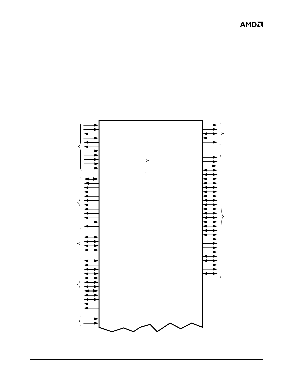
Signal Definitions 32580B
3.0Signal Definitions
3
This section defines the signals and describes the external
interface of the SC2200 processor. Figure 2-1 shows the
signals organized by their functional groups. Where signals
are multiplexed, the default signal name is listed first and is
POR#
X32I
X32O
X27I
System
Interface
Memory
Interface
ACCESS.bus
Interface
Parallel Port/
TFT Interface
X27O
PCIRST#
BOOT16+ROMCS#
LPC_ROM+PCICLK1
TFT_PRSNT+SDATA_OUT
FPCI_MON+PCICLK0
DID0+GNT0#, DID1+GNT1#
MD[63:0]
MA[12:0]
BA[1:0]
CS[1:0]#
RASA#
CASA#
WEA#
DQM[7:0]
CKEA
SDCLK[3:0]
SDCLK_IN
SDCLK_OUT
AB1C+GPIO20+DOCCS#
AB1D+GPIO1+IOCS1#
GPIO12+AB2C
GPIO13+AB2D
ACK#+TFTDE
AFD#/DSTRB#+TFTD2
BUSY/WAIT#+TFTD3
ERR#+TFTD4
INIT#+TFTD5
PD7+TFTD13
PD6+TFTD1
PD[5:0]+TFTD[11:6]
PE+TFTD14
SLCT+TFTD15
SLIN#/ASTRB#+TFTD16
STB#/WRITE#+TFTD17
AMD Geode™
SC2200
Processor
separated by a plus sign (+). A slash (/) in a signal name
means that the function is always enabled and available
(i.e., cycle multiplexed).
HSYNC
RED, GREEN, BLUE
Straps
IDE_ADDR2+TFTD4
IDE_ADDR1+TFTD2
IDE_ADDR0+TFTD3
IDE_DATA15+TFTD7
IDE_DATA14+TFTD17
IDE_DATA13+TFTD15
IDE_DATA12+TFTD13
IDE_DATA11+GPIO41
IDE_DATA10+DDC_SCL
IDE_DATA9+DDC_SDA
IDE_DATA8+GPIO40
IDE_DATA7+INTD#
IDE_DATA6+IRQ9
IDE_DATA5+CLK27M
IDE_DATA4+FP_VDD_ON
IDE_DATA3+TFTD12
IDE_DATA2+TFTD14
IDE_DATA1+TFTD16
IDE_DATA0+TFTD6
IDE_IOR0#+TFTD10
IDE_IOW0#+TFTD9
IDE_CS0#+TFTD5
IDE_CS1#+TFTDE
IDE_IORDY0+TFTD11
IDE_DREQ0+TFTD8
IDE_DACK0#+TFTD0
IDE_RST#+TFTDCK
VSYNC
VREF
SETRES
IRQ14+TFTD1
CRT
Interface
IDE/TFT
Interface
Video Port
Interface
VPD[7:0]
VPCKIN
Note: Straps are not the default signal, shown with system signals for reader convenience. However, they are also listed with the
appropriate functional group.
Figure 3-1. Signal Groups
AMD Geode™ SC2200 Processor Data Book 25
Page 26
32580B
Signal Definitions
USB
Interface
Serial Ports
(UARTs)/IDE
Interface
IR Port
Interface
AC97 Audio
Interface
Power
Management
Interface
JTAG
Interface
POWER_EN
OVER _CUR#
DPOS_PORT1
DNEG_PORT1
DPOS_PORT2
DNEG_PORT2
DPOS_PORT3
DNEG_PORT3
SIN1
SIN2+SDTEST3
SOUT1+CLKSEL1
SOUT2+CLKSEL2
GPIO7+RTS2#+IDE_DACK1#+SDTEST0
GPIO8+CTS2#+IDE_DREQ1+SDTEST4
GPIO18+DTR1#/BOUT1
GPIO6+DTR2#/BOUT2+IDE_IOR1#+SDTEST5
GPIO11+RI2#+IRQ15
GPIO9+DCD2#+IDE_IOW1#+SDTEST2
GPIO10+DSR2#+IDE_IORDY1+SDTEST1
IRRX1+SIN3
IRTX+SOUT3
BIT_CLK
SDATA_OUT+TFT_PRSNT
SDATA_IN
SDATA_IN2
SYNC+CLKSEL3
AC97_CLK
AC97_RST#
GPIO16+PC_BEEP
CLK32
GPWIO[2:0]
LED#
ONCTL#
PWRBTN#
PWRCNT[1:2]
THRM#
TCK
TDI
TDO
TMS
TRST#
AMD Geode™
SC2200
Processor
GPIO17+TFTDCK+IOCS0#
GPIO20+DOCCS#+TFTD0
GPIO15+DOCW#+IOW#
GPIO19+INTC#+IOCHRDY
GPIO38+IRRX2+LPCPD
TEST3+GXCLK+FP_VDD_ON
PCICLK0+FPCI_MON
PCICLK1+LPC_ROM
PCICLK
INTA#, INTB#
FRAME#
LOCK#
PERR#
SERR#
REQ[1:0]#
GNT0#+DID0
GNT1#+DID1
A[23:0]/AD[23:0]
D[7:0]/AD[31:24]
D[11:8]/C/BE[3:0]#
D12/PAR
D13/TRDY#
D14/IRDY#
D15/STOP#
BHE#/DEVSEL#
GPIO1+IOCS1+TFTD12
ROMCS#/BOOT16
RD#+CLKSEL0
WR#
GPIO14+DOCR#+IOR#
GPIO0+TRDE#
GPIO32+LAD0
GPIO33+LAD1
GPIO34+LAD2
GPIO35+LAD3
GPIO36+LDRQ#
GPIO37+LFRAME#
GPIO39+SERIRQ
TEST1+PLL6B
TEST0+PLL2B
TEST2+PLL5B
GTEST
TDP, TDN
Sub-ISA/PCI Bus
Interface
GPIO/LPC Bus
Interface
Test and
Measurement
Interface
Figure 3-1. Signal Groups (Continued)
The remaining subsections of this chapter describe:
• Section 3.1 "Ball Assignments": Provides a ball assignment diagram and tables listing the signals sorted
according to ball number and alphabetically by signal
name.
• Section 3.2 "Strap Options": Several balls are read at
power-up that set up the state of the SC2200. This
section provides details regarding those balls.
26 AMD Geode™ SC2200 Processor Data Book
• Section 3.3 "Multiplexing Configuration": Lists multi-
plexing options and their configurations.
• Section 3.4 "Signal Descriptions": Detailed descriptions
of each signal according to functional group.
Page 27
Signal Definitions
3.1 Ball Assignments
The SC2200 is highly configurable as illustrated in Figure
3-1 on page 25. Strap options and register programming
are used to set various modes of operation and specific
signals on specific balls. This section describes which signals are available on which balls and provides configuration
information:
• Figure 3-2 on page 28: Illustrates the BGU481 ball
assignments.
• Table 3-2 on page 29: Lists signals according to ball
number. Power Rail, Signal Type, Buffer Type and,
where relevant, Pull-Up or Pull-Down resistors are indicated for each ball in this table. For multiplexed balls, the
necessary configuration for each signal is listed as well.
• Table 3-3 on page 41: Quick reference signal list sorted
alphabetically - listing all signal names and ball
numbers.The tables in this chapter use several common
abbreviations. Table 3-1 lists the mnemonics and their
meanings
Notes:
1) For each GPIO signal, there is an optional pull-up
resistor on the relevant ball. After system reset, the
pull-up is present.
This pull-up resistor can be disabled via registers in
the Core Logic module. The configuration is without
regard to the selected ball function (except for
GPIO12, GPIO13, and GPIO16). Alternate functions
for GPIO12, GPIO13, and GPIO16 control pull-up
resistors.
For more information, see Section 6.4.1 "Bridge,
GPIO, and LPC Registers - Function 0" on page 198.
2) Configuration settings listed in this table are with
regard to the Pin Multiplexing Register (PMR). See
Section 4.2 "Multiplexing, Interrupt Selection, and
Base Address Registers" on page 76 for a detailed
description of this register.
32580B
Table 3-1. Signal Definitions Legend
Mnemonic Definition
A Analog
AV
SS
AV
CC
GCB General Configuration Block registers.
I Input ball
I/O Bidirectional ball
MCR[x] Miscellaneous Configuration Register
O Output ball
OD Open-drain
PD Pull-down in KΩ
PMR[x] Pin Multiplexing Register Bit x: A regis-
PU Pull-up in KΩ
TS TRI-STATE
V
CORE
V
IO
V
SS
# The # symbol in a signal name indicates
/ A / in a signal name indicates both func-
+ A + in signal name indicates the function
Ground ball: Analog
Power ball: Analog
Refer to Section 4.0 "General Configuration Block" on page 75.
Location of the General Configuration
Block cannot be determined by software.
See the AMD Geode™ SC2200 Proces-
sor Specification Update.
Bit x: A register, located in the GCB.
Refer to Section 4.1 "Configuration
Block Addresses" on page 75 for further
details.
ter, located in the GCB, used to configure balls with multiple functions. Refer to
Section 4.1 "Configuration Block
Addresses" on page 75 for further
details.
Power ball: 1.2V
Power ball: 3.3V
Ground ball
that the active or asserted state occurs
when the signal is at a low voltage level.
Otherwise, the signal is asserted when
at a high voltage level.
tions are always enabled (i.e., cycle multiplexed).
is available on the ball, but that either
strapping options or register programming is required to select the desired
function.
AMD Geode™ SC2200 Processor Data Book 27
Page 28
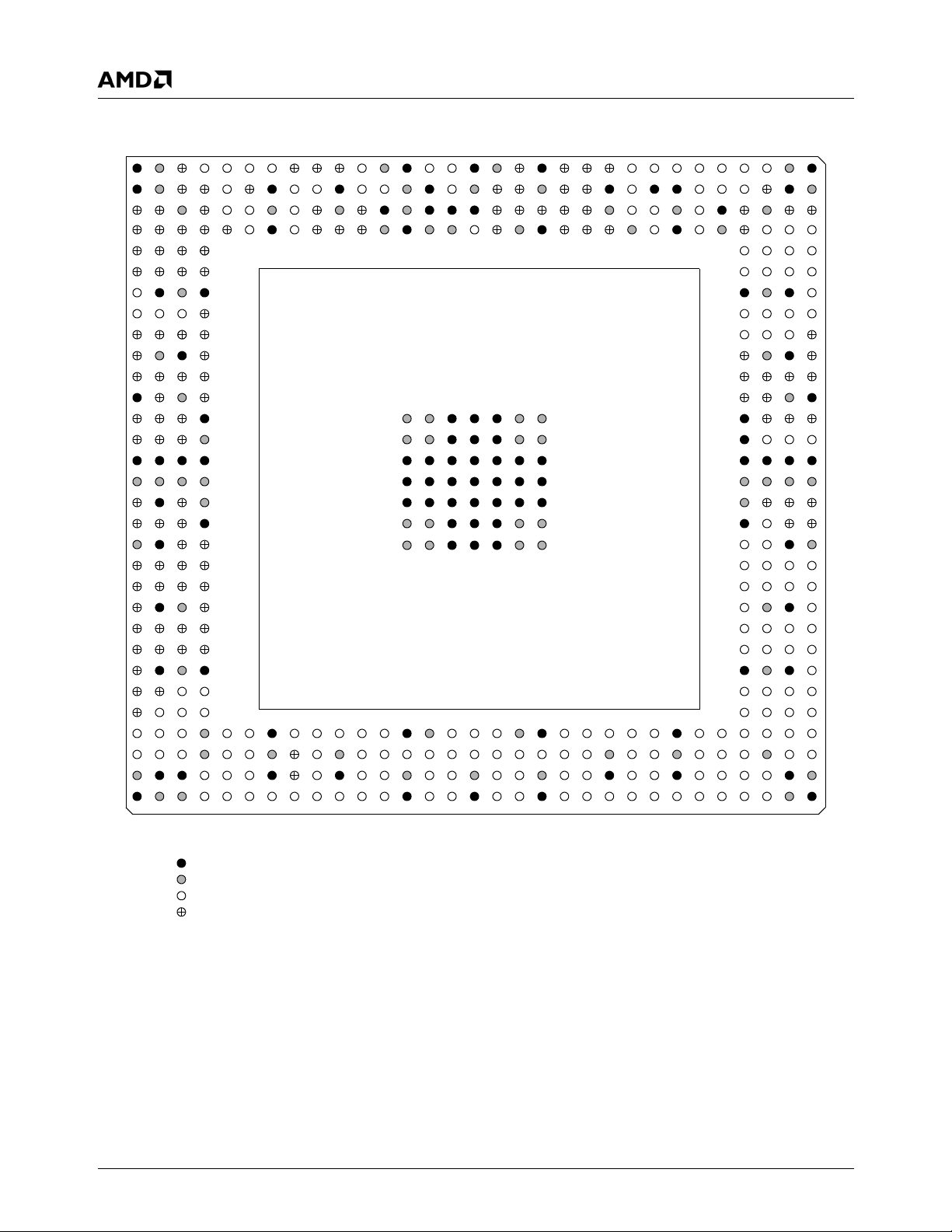
32580B
Signal Definitions
12345678910111213141516171819202122232425262728293031
SSVIOVSS
S
S
SSS
FRM# IOR# GP1 TRDE# V
SS
GREEN BLUE VSSV
CCCTVSS
STRES VIOBUSY ACK# VIOSLIN# INIT# VSSNC VSSVSSNC D+P2 D-P2 GP10 VSSV
SSCT
SSCTAVCCCTAVSSCTAVSSCTAVSSP2
CCCTVSSVIOAVCCCT
VREF PE VIOVSSPD2 ERR# AFD# VIONC VSSINTA# AV
PD7 VSSPD6 PD1 STB# NC NC N C D+P3 D-P3 D+P1 D-P1 VIOV
PLL2
SLCT PD4 PD5 PD3 PD0 VIONC NC VIOINTB# AV
SSUSB
CCUSB
AMD Geode™
AD14 GP38 VIOVSSGP37
IOVSS
SC2200 Processor
SS
CORE
CORE
SS
IDAT3
SSVIO
SSVIOVSS
S
PBTN# GPW0 VSSCK32 POR# MD3 MD5 WEA# VSSVIOMA1 MD34 MD37 VIOVSSMD41 MA9 MA8 DQM1 MD13 VSSMA11 CS1# MD18 MD48 MD20 MD51
IO
ONCT# GPW2 VIOGP11 MD0 VIOMD6 CASA# BA0 MA10 MD32 MD33 MD36 MD47 MD45 MD42 SDCK0 VIOMA6 MA3 VIOMD11 SDCKI MD19 VIOMD22 MD17
PLL3
THRM#GPW1 PCNT1 VSSIRRX1 MD1 VSSMD7 RASA# VIOBA1 MA2 VIOMD35 MD46 VIOMD43 DQM5 VSSMA5 MD15 VSSMD14 MD12 SDCKO MD16 VSSV
LED# VSBV
BAT
PCNT2 SDATI2 MD2 MD4 DQM0 CS0# VSSMA0 DQM4 VSSMD38 MD39 VSSMD44 MD40 CKEA MA7 MA4 MD8 MD10 MD9 MA12 MD23 VIOV
SBL
V
COREVCOREVSSVSSVSSVCOREVCORE
V
COREVCOREVSSVSSVSSVCOREVCORE
VSSVSSVSSVSSVSSVSSV
VSSVSSVSSVSSVSSVSSV
VSSVSSVSSVSSVSSVSSV
V
COREVCOREVSSVSSVSSVCOREVCORE
V
COREVCOREVSSVSSVSSVCOREVCORE
(Top View)
SS
SS
SS
GP9 VIOGP7 GP8
GP6 SOUT TDP TDN
TMS TDI GTST VPCKI
VSSVIOVSSVPD7
VPD6 VPD5 VPD4 VPD3
VPD2 VPD1 VPD0 GP39
GP36 GP35 GP34 GP33
GP32 GP13 V
VSSGP12 AB1D AB1C
V
CORE
V
SSVSSVSSVSS
V
COREVCOREVCOREVCORE
V
CORE
V
SS
MD57 SDCK1 V
MD58 MD59 MD60 MD56
SDCK2 MD61 MD62 MD63
MD24 V
MD25 MD26 MD27 DQM3
MD52 MD29 MD30 MD31
V
SSVIOVSS
MD50 MD49 MD54 MD53
MD21 DQM6 DQM2 MD55
A
VSSVIOAD30 PCK0 REQ1# PRST# PCICK IOW# GP20 GP17 HSNC AV
B
VSSVIOAD29 AD28 REQ0# AD23 VSSRD# WR# VSSVSNC RED VIOAV
C
AD26 AD24 VIOAD25 GNT0# GNT1# VIORMCS# GP19 VIOIRTX V
D
AD21 AD22 AD20 AD27 AD31 PCK1 V
E
AD16 AD19 AD18 DVSL# SIN2 TRST# TDO TCK
F
TRDY# IRDY# CBE2# AD17
G
STOP# V
H
SRR# PRR# LOCK# CBE3#
J
AD13 CBE1# AD15 PAR
K
AD11 V
L
CBE0# AD9 AD10 A D12
M
AD7 VIOAD8
V
SS
N
AD3 AD6 AD5 V
P
AD4 ICS1# AD1 V
R
V
SSVSSVSSVSS
T
V
COREVCOREVCOREVCORE
U
AD0 IAD2 AD2 V
V
IDAT15 IDAT14 IDAT13 V
W
VIOVSSIDAT12 IDAT11
Y
IDAT10 IDAT9 IDAT8 IIOR0#
AA
IRST# IDAT7 IDAT6 IDAT5
AB
IDAT4 V
AC
IDAT1 IDAT2 IDAT0 IDRQ0
AD
IIORY0 IIOW0# IAD0 IDACK0#
AE
IAD1 V
AF
IRQ14 ICS0# SOUT1 OVRCUR#
AG
GP18 SIN1 X27I TEST1
AH
PWRE X27O TEST0 V
AJ
TEST2 X32I X32O V
AK
V
IOVSSAVSSP3
AL
VSSVIOV
12345678910111213141516171819202122232425262728293031
Note: Signal names have been abbreviated in this figure due to space constraints.
= GND Ball
= PWR Ball
S
= Strap Option Ball
= Multiplexed Ball
SS
IOVSS
SS
SDO SYNC ACCK
ACRST# BITCK SDI
SDCK3 GXCK GP16
SSVIO
DQM7
IOVSS
MD28
A
SS
B
IO
C
D
E
F
G
H
J
K
L
M
N
P
R
T
U
V
W
Y
AA
AB
AC
AD
AE
AF
AG
AH
AJ
AK
IO
AL
SS
Figure 3-2. BGU481 Ball Assignment Diagram
28 AMD Geode™ SC2200 Processor Data Book
Page 29
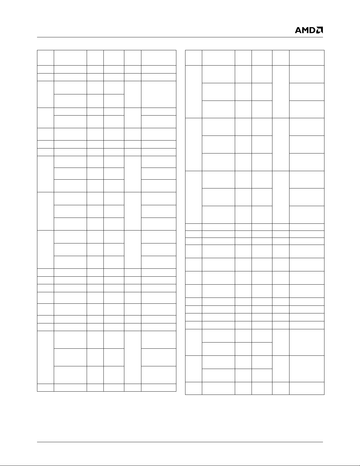
Signal Definitions
Table 3-2. BGU481 Ball Assignment - Sorted by Ball Number
1
O
O
STRP
, O
T
O
O
O
O
14/14
14/14
PCI
PCI
PCI
PCI
PCI
PCI
PCI
T
3/5
3/5
, O
3/5
1/4
, O
3/5
1/4
1/4
1/4
Power
,
,
3/5
3/5VIO
3/5VIO
Ball
No. Signal Name
A1 V
A2 V
SS
IO
I/O
Buffer
(PU/PD)
Typ e
GND --- --- ---
PWR --- --- ---
A3 AD30 I/O IN
D6 I/O IN
A4 PCICLK0 O O
FPCI_MON I
(PD
A5 REQ1# I
(PU
100
22.5
IN
)
IN
)
A6 PCIRST# O O
A7 PCICLK I IN
A8 IOW# O O
DOCW# O O
GPIO15 I/O
A9 GPIO20 I/O
(PU
(PU
22.5
22.5
IN
TS
)
IN
)
DOCCS# O
(PU
)
22.5
TFTD0 O
A10 GPIO17 I/O
IOCS0# O
(PU
(PU
(PU
22.5
22.5
22.5
)
IN
TS
)
)
TFTDCK O
(PU
)
22.5
A11 HSYNC O O
A12 AV
A13 V
CCCRT
SS
PWR --- --- ---
GND --- --- ---
A14 GREEN O WIRE AV
A15 BLUE O WIRE AV
A16 V
A17 V
A18
SS
PLL2
6, 2
PD7 I/O INT,
GND --- --- ---
PWR --- --- ---
O
TFTD13 O O
F_AD7 O O
A19 V
SS
GND --- --- ---
Rail Configuration
VIOCycle Multiplexed
VIO---
Strap (See Table
3-4 on page 45.)
VIO---
VIO---
VIO---
VIOPMR[21] = 0 and
PMR[2] = 0
PMR[21] = 0 and
PMR[2] = 1
PMR[21] = 1 and
PMR[2] = 1
PMR[23]3 = 0 and
PMR[7] = 0
PMR[23]3 = 0 and
PMR[7] = 1
PMR[23]3 = 1
PMR[23]3 = 0 and
PMR[5] = 0
PMR[23]3 = 0 and
PMR[5] = 1
PMR[23]3 = 1
VIO---
---
C-
CCRT
---
C-
CCRT
V
IO
PMR[23]3 = 0 and
(PMR[27] = 0 and
FPCI_MON = 0)
PMR[23]3 = 1 and
(PMR[27] = 0 and
FPCI_MON = 0)
PMR[23]3 = 0 and
(PMR[27] = 1 or
FPCI_MON = 1)
32580B
1
O
O
O
O
O
14/14
1/4
14/14
14/14
1/4
14/14
14/14
1/4
14/14
USB
USB
USB
USB
USB
USB
USB
USB
PCI
PCI
PCI
PCI
PCI
PCI
PCI
PCI
PCI
Power
Rail Configuration
V
IO
V
IO
V
IO
,
AV
C-
CUSB
,
AV
C-
CUSB
,
AV
C-
CUSB
,
AV
C-
CUSB
,
VIOCycle Multiplexed
,
,
VIOCycle Multiplexed
,
VIO---
Ball
No. Signal Name
6, 2
PD6 I/O INT,
A20
I/O
(PU/PD)
Buffer
Typ e
O
TFTD1 O O
F_AD6 O O
6, 2
PD1 I/O INT,
A21
O
TFTD7 O O
F_AD1 O O
6, 2
STB#/WRITE# O O
A22
TFTD17 O
F_FRAME# O O
A23 NC --- --- --- ---
A24 NC --- --- --- ---
A25 NC --- --- --- ---
6
DPOS_PORT3 I/O IN
A26
6
DNEG_PORT3 I/O IN
A27
6
DPOS_PORT1 I/O IN
A28
6
DNEG_PORT1 I/O IN
A29
A30 V
A31 V
B1 V
B2 V
IO
SS
SS
IO
PWR --- --- ---
GND --- --- ---
GND --- --- ---
PWR --- --- ---
O
O
O
O
B3 AD29 I/O IN
D5 I/O IN
B4 AD28 I/O IN
D4 I/O IN
B5 REQ0# I
(PU
22.5
IN
)
PMR[23]3 = 0 and
(PMR[27] = 0 and
FPCI_MON = 0)
PMR[23]3 = 1 and
(PMR[27] = 0 and
FPCI_MON = 0
PMR[23]3 = 0 and
(PMR[27] = 1 or
FPCI_MON = 1)
PMR[23]3 = 0 and
(PMR[27] = 0 and
FPCI_MON = 0)
PMR[23]3 = 1 and
(PMR[27] = 0 and
FPCI_MON = 0)
PMR[23]3 = 0 and
(PMR[27] = 1 or
FPCI_MON = 1)
PMR[23]3 = 0 and
(PMR[27] = 0 and
FPCI_MON = 0)
PMR[23]3 = 1 and
(PMR[27] = 0 and
FPCI_MON = 0)
PMR[23]3 = 0 and
(PMR[27] = 1 or
FPCI_MON = 1)
---
---
---
---
AMD Geode™ SC2200 Processor Data Book 29
Page 30
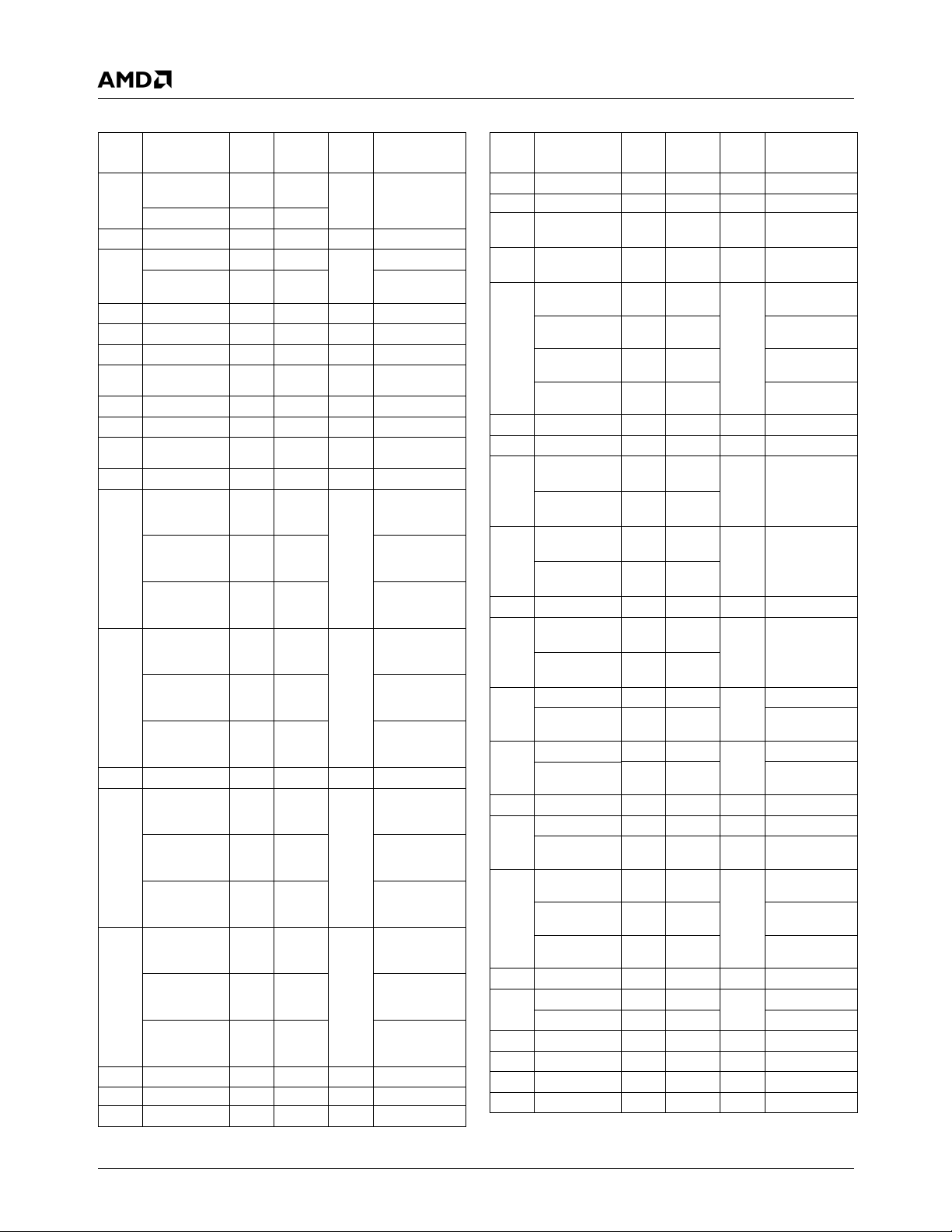
32580B
Table 3-2. BGU481 Ball Assignment - Sorted by Ball Number (Continued)
1
O
STRP
14/14
14/14
14/14
14/14
Power
Rail Configuration
,
VIOCycle Multiplexed
PCI
PCI
PCI
VIO---
3/5
V
3/5
1/4
1/4
1/4
1/4
1/4
1/4
1/4
IO
VIO---
C-
CCRT
C-
CCRT
V
T
IO
V
T
IO
V
IO
V
IO
Ball
No. Signal Name
I/O
(PU/PD)
Buffer
Typ e
B6 AD23 I/O IN
A23 O O
B7 V
SS
GND --- --- ---
B8 RD# O O
CLKSEL0 I
(PD
100
IN
)
B9 WR# O O
B10 V
SS
GND --- --- ---
B11 VSYNC O O
B12 RED O WIRE AV
B13 V
B14 AV
IO
SSCRT
PWR --- --- ---
GND --- --- ---
B15 SETRES I WIRE AV
B16 V
B17
IO
6, 2
BUSY/WAIT# I IN
PWR --- --- ---
TFTD3 O O
F_C/BE1# O O
6, 2
ACK# I IN
B18
TFTDE O O
FPCICLK O O
B19 V
B20
IO
6,2
SLIN#/ASTRB# O O
PWR --- --- ---
TFTD16 O O
F_IRDY# O O
6,2
INIT# O O
B21
TFTD5 O O
SMI_O O O
B22 V
SS
GND --- --- ---
B23 NC --- --- --- ---
B24 V
SS
GND --- --- ---
Strap (See Table
3-4 on page 45.)
---
---
PMR[23]3 = 0 and
(PMR[27] = 0 and
FPCI_MON = 0)
PMR[23]3 = 1 and
(PMR[27] = 0 and
FPCI_MON = 0)
PMR[23]3 = 0 and
(PMR[27] = 1 or
FPCI_MON = 1)
PMR[23]3 = 0 and
(PMR[27] = 0 and
FPCI_MON = 0)
PMR[23]3 = 1 and
(PMR[27] = 0 and
FPCI_MON = 0)
PMR[23]3 = 0 and
(PMR[27] = 1 or
FPCI_MON = 1)
PMR[23]3 = 0 and
(PMR[27] = 0 and
FPCI_MON = 0)
PMR[23]3 = 1 and
(PMR[27] = 0 and
FPCI_MON = 0)
PMR[23]3 = 0 and
(PMR[27] = 1 or
FPCI_MON = 1)
PMR[23]3 = 0 and
(PMR[27] = 0 and
FPCI_MON = 0)
PMR[23]3 = 1 and
(PMR[27] = 0 and
FPCI_MON = 0)
PMR[23]3 = 0 and
(PMR[27] = 1 or
FPCI_MON = 1)
Signal Definitions
1
USB
USB
USB
USB
IN
O
O
O
O
O
O
O
STRP
STRP
STRP
IN
Power
Rail Configuration
,
AV
C-
CUSB
,
AV
C-
CUSB
, O
8/8VIO
TS
TS1
2/5
,
VIOCycle Multiplexed
PCI
PCI
,
PCI
PCI
,
VIOCycle Multiplexed
PCI
PCI
,
PCI
PCI
,
VIOCycle Multiplexed
PCI
PCI
,
PCI
PCI
VIO---
PCI
VIO---
PCI
VIO---
3/5
VIOStrap (See Table
, O
3/5VIO
TS
TS1
VIOPMR[6] = 0
8/8
8/8
Ball
No. Signal Name
B25 V
SS
I/O
Buffer
(PU/PD)
Typ e
GND --- --- ---
B26 NC --- --- --- ---
6
DPOS_PORT2 I/O IN
B27
6
DNEG_PORT2 I/O IN
B28
B29 GPIO10 I/O
(PU
DSR2# I
IDE_IORDY1 I
SDTEST1 O
B30 V
B31 V
SS
IO
(PU
(PU
(PU
GND --- --- ---
PWR --- --- ---
22.5
22.5
22.5
22.5
O
O
IN
TS
)
)
IN
)
)
C1 AD26 I/O IN
D2 I/O IN
C2 AD24 I/O IN
D0 I/O IN
C3 V
IO
PWR --- --- ---
C4 AD25 I/O IN
D1 I/O IN
C5 GNT0# O O
DID0 I
(PD
100
IN
)
C6 GNT1# O O
DID1 I
C7 V
(PD
IO
IN
)
100
PWR --- --- ---
C8 ROMCS# O O
BOOT16 I
(PD
C9 GPIO19 I/O
INTC# I
IOCHRDY I
C10 V
IO
(PU
(PU
(PU
IN
)
100
IN
TS
)
22.5
)
22.5
IN
)
22.5
PWR --- --- ---
C11 IRTX O O
SOUT3 O O
C12 V
C13 AV
C14 AV
C15 AV
SSCRT
CCCRT
SSCRT
SSCRT
GND --- --- ---
PWR --- --- ---
GND --- --- ---
GND --- --- ---
---
---
PMR[18] = 0 and
PMR[8] = 0
PMR[18] = 1 and
PMR[8] = 0
PMR[18] = 0 and
PMR[8] = 1
PMR[18] = 1 and
PMR[8] = 1
Strap (See Table
3-4 on page 45.)
Strap (See Table
3-4 on page 45.)
3-4 on page 45.)
PMR[9] = 0 and
PMR[4] = 0
PMR[9] = 0 and
PMR[4] = 1
PMR[9] = 1 and
PMR[4] = 1
PMR[6] = 1
30 AMD Geode™ SC2200 Processor Data Book
Page 31

Signal Definitions
Table 3-2. BGU481 Ball Assignment - Sorted by Ball Number (Continued)
1
14/14
14/14
14/14
14/14
14/14
14/14
14/14
14/14
, O
IN
O
O
Power
Rail Configuration
V
T
IO
1/4
1/4
,
V
T
IO
1/4
V
IO
1/4
V
IO
1/4
V
IO
1/4
VIO---
PCI
1/4VIO
TS
1/4
2/5
Ball
No. Signal Name
C16 AV
C17
SSPLL2
6,2
SLCT I IN
I/O
Buffer
(PU/PD)
Typ e
GND --- --- ---
TFTD15 O O
F_C/BE3# O O
C18 PD4 I/O IN
O
TFTD10 O O
F_AD4 O O
6,2
PD5 I/O INT,
C19
O
TFTD11 O O
F_AD5 O O
6,2
PD3 I/O INT,
C20
O
TFTD9 O O
F_AD3 O O
6,2
PD0 I/O INT,
C21
O
TFTD6 O O
F_AD0 O O
C22 V
IO
PWR --- --- ---
C23 NC --- --- --- ---
C24 NC --- --- --- ---
C25 V
IO
C26 INTB# I
C27 AV
SSUSB
C28 GPIO9 I/O
DCD2# I
IDE_IOW1# O
PWR --- --- ---
IN
)
(PU
22.5
GND --- --- ---
IN
TS
)
(PU
22.5
)
(PU
22.5
)
(PU
22.5
SDTEST2 O
)
(PU
22.5
PMR[23]3 = 0 and
(PMR[27] = 0 and
FPCI_MON = 0)
PMR[23]3 = 1 and
(PMR[27] = 0 and
FPCI_MON = 0)
PMR[23]3 = 0 and
(PMR[27] = 1 or
FPCI_MON = 1)
PMR[23]3 = 0 and
(PMR[27] = 0 and
FPCI_MON = 0)
PMR[23]3 = 1 and
(PMR[27] = 0 and
FPCI_MON = 0)
PMR[23]3 = 0 and
(PMR[27] = 1 or
FPCI_MON = 1)
PMR[23]3 = 0 and
(PMR[27] = 0 and
FPCI_MON = 0)
PMR[23]3 = 1 and
(PMR[27] = 0 and
FPCI_MON = 0)
PMR[23]3 = 0 and
(PMR[27] = 1 or
FPCI_MON = 1)
PMR[23]3 = 0 and
(PMR[27] = 0 and
FPCI_MON = 0)
PMR[23]3 = 1 and
(PMR[27] = 0 and
FPCI_MON = 0)
PMR[23]3 = 0 and
(PMR[27] = 1 or
FPCI_MON = 1)
PMR[23]3 = 0 and
(PMR[27] = 0 and
FPCI_MON = 0)
PMR[23]3 = 1 and
(PMR[27] = 0 and
FPCI_MON = 0)
PMR[23]3 = 0 and
(PMR[27] = 1 or
FPCI_MON = 1)
PMR[18] = 0 and
PMR[8] = 0
PMR[18] = 1 and
PMR[8] = 0
PMR[18] = 0 and
PMR[8] = 1
PMR[18] = 1 and
PMR[8] = 1
32580B
Ball
No. Signal Name
C29 V
IO
C30 GPIO7 I/O
RTS2# O
IDE_DACK1# O
SDTEST0 O
C31 GPIO8 I/O
CTS2# I
IDE_DREQ1 I
SDTEST4 O
D1 AD21 I/O IN
A21 O O
D2 AD22 I/O IN
A22 O O
D3 AD20 I/O IN
A20 O O
D4 AD27 I/O IN
D3 I/O IN
D5 AD31 I/O IN
D7 I/O IN
D6 PCICLK1 O O
LPC_ROM I
D7 V
SS
D8 FRAME# I/O
D9 IOR# O O
DOCR# O O
GPIO14 I/O
D10 GPIO1 I/O
IOCS1# O
TFTD12 O
D11 TRDE# O O
GPIO0 I/O
D12 V
CCCRT
I/O
(PU/PD)
Buffer
PWR --- --- ---
IN
)
(PU
22.5
(PU
)
22.5
(PU
)
22.5
)
(PU
22.5
IN
)
(PU
22.5
)
(PU
22.5
)
(PU
22.5
)
(PU
22.5
IN
)
(PD
100
GND --- --- ---
IN
)
(PU
22.5
IN
)
(PU
22.5
IN
)
(PU
22.5
(PU
)
22.5
(PU
)
22.5
IN
)
(PU
22.5
PWR --- --- ---
Typ e
, O
TS
O
1/4
O
1/4
O
2/5
, O
TS
IN
IN
TS1
O
2/5
PCI
O
PCI
PCI
PCI
O
PCI
PCI
PCI
O
PCI
PCI
PCI
O
PCI
PCI
O
PCI
PCI
O
PCI
PCI
O
PCI
PCI
STRP
PCI
O
PCI
3/5
3/5
, O
TS
, O
T
O
3/5
O
1/4
3/5
, O
TS
TS
1
Power
Rail Configuration
1/4VIO
PMR[17] = 0 and
PMR[8] = 0
PMR[17] = 1 and
PMR[8] = 0
PMR[17] = 0 and
PMR[8] = 1
PMR[17] = 1 and
PMR[8] = 1
8/8VIO
PMR[17] = 0 and
PMR[8] = 0
PMR[17] = 1 and
PMR[8] = 0
PMR[17] = 0 and
PMR[8] = 1
PMR[17] = 1 and
PMR[8] = 1
,
VIOCycle Multiplexed
,
VIOCycle Multiplexed
,
VIOCycle Multiplexed
,
VIOCycle Multiplexed
,
,
VIOCycle Multiplexed
,
VIO---
Strap (See Table
3-4 on page 45.)
,
VIO---
VIOPMR[21] = 0 and
PMR[2] = 0
PMR[21] = 0 and
PMR[2] = 1
3/5
3/5VIO
PMR[21] = 1 and
PMR[2] = 1
PMR[23]3 = 0 and
PMR[13] = 0
V
IO
PMR[23]3 = 0 and
PMR[13] = 1
V
IO
PMR[23]3 = 1
VIOPMR[12] = 0
3/5VIO
PMR[12] = 1
AMD Geode™ SC2200 Processor Data Book 31
Page 32

32580B
Table 3-2. BGU481 Ball Assignment - Sorted by Ball Number (Continued)
1
IN
14/14
14/14
14/14
14/14
O
O
O
T
1/4
1/4
1/4
1/4
1/4
1/4
PCI
, O
1/4
1/4
2/5
Power
Rail Configuration
C-
CCRT
V
IO
V
IO
1/4VIO
V
IO
VIO---
1/4VIO
Ball
No. Signal Name
D13 V
D14 V
D15 AV
SS
IO
CCCRT
I/O
Buffer
(PU/PD)
Typ e
GND --- --- ---
PWR --- --- ---
PWR --- --- ---
D16 VREF I/O WIRE AV
6, 2
PE I
D17
(PU
PD
22.5
22.5
)
TFTD14 O O
F_C/BE2# O O
D18 V
D19 V
D20
IO
SS
6, 2
PD2 I/O INT,
PWR --- --- ---
GND --- --- ---
O
TFTD8 O O
F_AD2 O O
6, 2
ERR# I INT, O
D21
TFTD4 O O
F_C/BE0# O O
6, 2
AFD#/DSTRB# O O
D22
TFTD2 O O
INTR_O O O
D23 V
IO
PWR --- --- ---
D24 NC --- --- --- ---
D25 V
SS
D26 INTA# I
D27 AV
CCUSB
D28 GPIO6 I/O
DTR2#/BOUT2 O
IDE_IOR1# O
SDTEST5 O
GND --- --- ---
IN
)
(PU
22.5
PWR --- --- ---
IN
TS
)
(PU
22.5
)
(PU
22.5
)
(PU
22.5
)
(PU
22.5
---
PMR[23]3 = 0 and
(PMR[27] = 0 and
FPCI_MON = 0)
(PU/PD under
software control.)
PMR[23]3 = 1 and
(PMR[27] = 0 and
FPCI_MON = 0)
PMR[23]3 = 0 and
(PMR[27] = 1 or
FPCI_MON = 1)
PMR[23]3 = 0 and
(PMR[27] = 0 and
FPCI_MON = 0)
PMR[23]3 = 1 and
(PMR[27] = 0 and
FPCI_MON = 0)
PMR[23]3 = 0 and
(PMR[27] = 1 or
FPCI_MON = 1)
PMR[23]3 = 0 and
(PMR[27] = 0 and
FPCI_MON = 0)
PMR[23]3 = 1 and
(PMR[27] = 0 and
FPCI_MON = 0)
PMR[23]3 = 0 and
(PMR[27] = 1 or
FPCI_MON = 1)
PMR[23]3 = 0 and
(PMR[27] = 0 and
FPCI_MON = 0)
PMR[23]3 = 1 and
(PMR[27] = 0 and
FPCI_MON = 0)
PMR[23]3 = 0 and
(PMR[27] = 1 or
FPCI_MON = 1)
PMR[18] = 0 and
PMR[8] = 0
PMR[18] = 1 and
PMR[8] = 0
PMR[18] = 0 and
PMR[8] = 1
PMR[18] = 1 and
PMR[8] = 1
Signal Definitions
)
)
)
)
)
)
)
)
)
)
)
)
)
)
Buffer
Typ e
8/8
IN
STRP
PCI
O
PCI
PCI
PCI
O
PCI
PCI
PCI
O
PCI
PCI
IN
PCI
O
PCI
PCI
TS
2/5
IN
PCI
PCI
IN
PCI
IN
PCI
O
PCI
IN
PCI
O
PCI
IN
PCI
O
PCI
IN
PCI
O
PCI
IN
PCI
O
PCI
IN
PCI
O
PCI
PCI
O
PCI
PCI
IN
PCI
IN
PCI
IN
T
T
IN
PCI
O
PCI
IN
PCI
O
PCI
1
Power
Rail Configuration
VIO---
IO
,
VIOCycle Multiplexed
,
VIOCycle Multiplexed
,
VIOCycle Multiplexed
,
VIOCycle Multiplexed
VIOPMR[28] = 0
VIO---
VIO---
VIO---
,
VIOCycle Multiplexed
,
,
VIOCycle Multiplexed
,
,
VIOCycle Multiplexed
,
,
VIOCycle Multiplexed
VIO---
VIO---
VIO---
VIO---
,
VIOCycle Multiplexed
,
Ball
No. Signal Name
I/O
(PU/PD)
D29 SOUT2 O O
CLKSEL2 I
)
(PD
100
D30 TDP I/O Diode --- ---
D31 TDN I/O WIRE V
E1 AD16 I/O IN
A16 O O
E2 AD19 I/O IN
A19 O O
E3 AD18 I/O IN
A18 O O
E4 DEVSEL# I/O
(PU
22.5
BHE# O O
E28 SIN2 I IN
SDTEST3 O O
E29 TRST# I
(PU
22.5
E30 TDO O O
E31 TCK I
(PU
22.5
F1 TRDY# I/O
(PU
22.5
D13 I/O
(PU
22.5
F2 IRDY# I/O
(PU
22.5
D14 I/O
(PU
22.5
F3 C/BE2# I/O
D10 I/O
(PU
(PU
22.5
22.5
F4 AD17 I/O IN
A17 O O
F28 TMS I
(PU
22.5
F29 TDI I
F30 GTEST I
(PU
(PD
22.5
22.5
F31 VPCKIN I IN
G1 STOP# I/O
D15 I/O
G2 V
G3 V
G4 V
G28 V
SS
IO
SS
SS
(PU
22.5
(PU
22.5
GND --- --- ---
PWR --- --- ---
GND --- --- ---
GND --- --- ---
Strap (See Table
3-4 on page 45.)
---
PMR[28] = 1
32 AMD Geode™ SC2200 Processor Data Book
Page 33
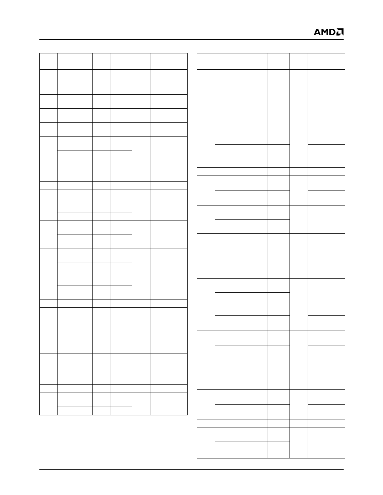
Signal Definitions
Table 3-2. BGU481 Ball Assignment - Sorted by Ball Number (Continued)
Ball
No. Signal Name
G29 V
G30 V
IO
SS
G31 VPD7 I IN
H1 SERR# I/O
H2 PERR# I/O
H3 LOCK# I/O
H4 C/BE3# I/O
D11 I/O
H28 VPD6 I IN
H29 VPD5 I IN
H30 VPD4 I IN
H31 VPD3 I IN
J1 AD13 I/O IN
A13 O O
J2 C/BE1# I/O
D9 I/O
J3 AD15 I/O IN
A15 O O
J4 PAR I/O
D12 I/O
J28 VPD2 I IN
J29 VPD1 I IN
J30 VPD0 I IN
J31 GPIO39 I/O
SERIRQ I/O IN
K1 AD11 I/O IN
A11 O O
K2 V
K3 V
IO
SS
K4 AD14 I/O IN
A14 O O
I/O
Buffer
(PU/PD)
Typ e
PWR --- --- ---
GND --- --- ---
22.5
22.5
IN
)
OD
IN
)
(PU
(PU
IN
)
(PU
22.5
IN
)
(PU
22.5
IN
)
(PU
22.5
IN
)
(PU
22.5
IN
)
(PU
22.5
IN
)
(PU
22.5
22.5
22.5
IN
)
IN
)
(PU
(PU
PWR --- --- ---
GND --- --- ---
32580B
1
Power
Rail Configuration
VIO---
T
,
VIO---
PCI
PCI
,
VIO---
PCI
O
PCI
,
VIO---
PCI
O
PCI
,
VIOCycle Multiplexed
PCI
O
PCI
,
PCI
O
PCI
VIO---
T
VIO---
T
VIO---
T
VIO---
T
,
VIOCycle Multiplexed
PCI
O
PCI
PCI
,
VIOCycle Multiplexed
PCI
O
PCI
,
PCI
O
PCI
,
VIOCycle Multiplexed
PCI
O
PCI
PCI
,
VIOCycle Multiplexed
PCI
O
PCI
,
PCI
O
PCI
VIO---
T
VIO---
T
VIO---
T
,
V
PCI
O
PCI
PCI
O
PCI
PCI
O
PCI
PCI
PCI
O
PCI
PCI
IO
PMR[14]4 = 0 and
PMR[22]
,
PMR[14]4 = 1 and
PMR[22]
,
VIOCycle Multiplexed
,
VIOCycle Multiplexed
4
4
= 0
= 1
Ball
No. Signal Name
K28 GPIO38/IRRX2 I/O
I/O
(PU/PD)
(PU
22.5
LPCPD# O O
K29 V
K30 V
IO
SS
K31 GPIO37 I/O
PWR --- --- ---
GND --- --- ---
(PU
22.5
LFRAME# O O
L1 C/BE0# I/O
D8 I/O
(PU
(PU
22.5
22.5
L2 AD9 I/O IN
A9 O O
L3 AD10 I/O IN
A10 O O
L4 AD12 I/O IN
A12 O O
L28 GPIO36 I/O
(PU
22.5
LDRQ# I IN
L29 GPIO35 I/O
(PU
22.5
LAD3 I/O
(PU
22.5
L30 GPIO34 I/O
LAD2 I/O
L31 GPIO33 I/O
LAD1 I/O
M1 V
SS
(PU
22.5
(PU
22.5
(PU
22.5
(PU
22.5
GND --- --- ---
M2 AD7 I/O IN
A7 O O
M3 V
IO
PWR --- --- ---
)
)
)
)
)
)
)
)
)
)
)
Buffer
Typ e
IN
PCI
O
PCI
PCI
IN
PCI
O
PCI
PCI
IN
PCI
O
PCI
IN
PCI
O
PCI
PCI
O
PCI
PCI
PCI
O
PCI
PCI
PCI
O
PCI
PCI
IN
PCI
O
PCI
PCI
IN
PCI
O
PCI
IN
PCI
O
PCI
IN
PCI
O
PCI
IN
PCI
O
PCI
IN
PCI
O
PCI
IN
PCI
O
PCI
PCI
O
PCI
PCI
1
Power
Rail Configuration
,
V
IO
PMR[14]4 = 0 and
PMR[22]
The IRRX2 input
is connected to
the input path of
GPIO38. There is
no logic required
to enable IRRX2,
just a simple connection. Hence,
when GPIO38 is
the selected function, IRRX2 is
also selected.
PMR[14]4 = 1 and
PMR[22]
,
V
IO
PMR[14]4 = 0 and
PMR[22]
PMR[14]4 = 1 and
PMR[22]
,
VIOCycle Multiplexed
,
,
VIOCycle Multiplexed
,
VIOCycle Multiplexed
,
VIOCycle Multiplexed
,
V
IO
PMR[14]4 = 0 and
PMR[22]
PMR[14]4 = 1 and
PMR[22]
,
V
IO
PMR[14]4 = 0 and
PMR[22]
,
PMR[14]4 = 1 and
PMR[22]
,
V
IO
PMR[14]4 = 0 and
PMR[22]
,
PMR[14]4 = 1 and
PMR[22]
,
V
IO
PMR[14]4 = 0 and
PMR[22]
,
PMR[14]4 = 1 and
PMR[22]
,
VIOCycle Multiplexed
4
= 0.
4
= 1
4
= 0
4
= 1
4
= 0
4
= 1
4
= 0
4
= 1
4
= 0
4
= 1
4
= 0
4
= 1
AMD Geode™ SC2200 Processor Data Book 33
Page 34
32580B
Table 3-2. BGU481 Ball Assignment - Sorted by Ball Number (Continued)
Ball
No. Signal Name
M4 AD8 I/O IN
A8 O O
M28 GPIO32 I/O
LAD0 I/O
M29 GPIO13 I/O
AB2D I/O
M30 V
M31 V
IO
SS
N1 AD3 I/O IN
A3 O O
N2 AD6 I/O IN
A6 O
N3 AD5 I/O IN
A5 O O
N4 V
N13 V
N14 V
N15 V
N16 V
N17 V
N18 V
N19 V
N28 V
SS
CORE
CORE
SS
SS
SS
CORE
CORE
SS
N29 GPIO12 I/O
AB2C I/O
N30 AB1D I/O
GPIO1 I/O
IOCS1# O O
N31 AB1C I/O
GPIO20 I/O
DOCCS# O O
P1 AD4 I/O IN
A4 O O
P2 IDE_CS1# O O
TFTDE O O
I/O
22.5
22.5
Buffer
)
)
(PU/PD)
(PU
(PU
IN
)
(PU
22.5
IN
)
(PU
22.5
PWR --- --- ---
GND --- --- ---
GND --- --- ---
PWR --- --- ---
PWR --- --- ---
GND --- --- ---
GND --- --- ---
GND --- --- ---
PWR --- --- ---
PWR --- --- ---
GND --- --- ---
IN
)
(PU
22.5
IN
)
(PU
22.5
IN
)
(PU
22.5
22.5
22.5
IN
)
IN
)
(PU
(PU
IN
)
(PU
22.5
1
Typ e
IN
IN
AB
AB
AB
AB
AB
Power
Rail Configuration
,
VIOCycle Multiplexed
PCI
O
PCI
PCI
,
V
PCI
O
PCI
PCI
O
PCI
, O
,
8/8VIO
IO
PMR[14]4 = 0 and
PMR[22]
PMR[14]4 = 1 and
PMR[22]
PMR[19] = 0
, OD8VIOPMR[19] = 1
,
VIOCycle Multiplexed
PCI
O
PCI
PCI
,
VIOCycle Multiplexed
PCI
O
PCI
PCI
O
,
VIOCycle Multiplexed
PCI
O
PCI
PCI
, O
8/8VIO
, OD
8
, OD8V
, O
T
3/5
3/5
PMR[19] = 0
PMR[19] = 1
IO
PMR[23]3 = 0
PMR[23]3 = 1 and
PMR[13] = 0
PMR[23]3 = 1 and
PMR[13] = 1
, OD8V
AB
, O
T
3/5
PCI
O
PCI
PCI
1/4
1/4
IO
PMR[23]3 = 0
3/5
,
PMR[23]3 = 1 and
PMR[7] = 0
PMR[23]3 = 1 and
PMR[7] = 1
VIOCycle Multiplexed
VIOPMR[24] = 0
PMR[24] = 1
4
= 0
4
= 1
Ball
No. Signal Name
I/O
(PU/PD)
Buffer
P3 AD1 I/O IN
A1 O O
P4 V
P13 V
P14 V
P15 V
P16 V
P17 V
P18 V
P19 V
P28 V
CORE
CORE
CORE
SS
SS
SS
CORE
CORE
CORE
PWR --- --- ---
PWR --- --- ---
PWR --- --- ---
GND --- --- ---
GND --- --- ---
GND --- --- ---
PWR --- --- ---
PWR --- --- ---
PWR --- --- ---
P29 SDATA_OUT O O
TFT_PRSNT I
(PD
100
IN
)
P30 SYNC O O
CLKSEL3 I
(PD
100
IN
)
P31 AC97_CLK O O
R1 V
R2 V
R3 V
R4 V
R13 V
R14 V
R15 V
R16 V
R17 V
R18 V
R19 V
R28 V
R29 V
R30 V
R31 V
T1 V
T2 V
T3 V
T4 V
T13 V
T14 V
T15 V
T16 V
T17 V
T18 V
T19 V
T28 V
T29 V
SS
SS
SS
SS
SS
SS
SS
SS
SS
SS
SS
SS
SS
SS
SS
CORE
CORE
CORE
CORE
SS
SS
SS
SS
SS
SS
SS
CORE
CORE
GND --- --- ---
GND --- --- ---
GND --- --- ---
GND --- --- ---
GND --- --- ---
GND --- --- ---
GND --- --- ---
GND --- --- ---
GND --- --- ---
GND --- --- ---
GND --- --- ---
GND --- --- ---
GND --- --- ---
GND --- --- ---
GND --- --- ---
PWR --- --- ---
PWR --- --- ---
PWR --- --- ---
PWR --- --- ---
GND --- --- ---
GND --- --- ---
GND --- --- ---
GND --- --- ---
GND --- --- ---
GND --- --- ---
GND --- --- ---
PWR --- --- ---
PWR --- --- ---
Typ e
PCI
O
PCI
PCI
AC97
STRP
AC97
STRP
2/5
Signal Definitions
1
Power
Rail Configuration
,
VIOCycle Multiplexed
VIO---
VIOStrap (See Table
3-4 on page 45.)
VIO---
Strap (See Table
3-4 on page 45.)
VIOPMR[25] = 1
34 AMD Geode™ SC2200 Processor Data Book
Page 35
Signal Definitions
Table 3-2. BGU481 Ball Assignment - Sorted by Ball Number (Continued)
Ball
No. Signal Name
T30 V
T31 V
CORE
CORE
U1 AD0 I/O IN
A0 O O
U2 IDE_ADDR2 O O
TFTD4 O O
U3 AD2 I/O IN
A2 O O
U4 V
U13 V
U14 V
U15 V
U16 V
U17 V
U18 V
U19 V
U28 V
CORE
SS
SS
SS
SS
SS
SS
SS
CORE
U29 AC97_RST# O O
F_STOP# O O
U30 BIT_CLK I IN
F_TRDY# O O
U31 SDATA_IN I IN
F_GNT0# O O
V1 IDE_DATA15 I/O IN
TFTD7 O O
V2 IDE_DATA14 I/O IN
TFTD17 O O
V3 IDE_DATA13 I/O IN
TFTD15 O O
V4 V
V13 V
V14 V
V15 V
V16 V
V17 V
V18 V
V19 V
V28 V
SS
CORE
CORE
SS
SS
SS
CORE
CORE
SS
V29 SDCLK3 O O
V30 GXCLK O O
FP_VDD_ON O O
TEST3 O O
I/O
Buffer
(PU/PD)
Typ e
PWR --- --- ---
PWR --- --- ---
PWR --- --- ---
GND --- --- ---
GND --- --- ---
GND --- --- ---
GND --- --- ---
GND --- --- ---
GND --- --- ---
GND --- --- ---
PWR --- --- ---
TS
TS
TS
GND --- --- ---
PWR --- --- ---
PWR --- --- ---
GND --- --- ---
GND --- --- ---
GND --- --- ---
PWR --- --- ---
PWR --- --- ---
GND --- --- ---
32580B
1
Power
Rail Configuration
,
VIOCycle Multiplexed
PCI
O
PCI
PCI
VIOPMR[24] = 0
1/4
1/4
,
PCI
O
PCI
PCI
PMR[24] = 1
VIOCycle Multiplexed
Ball
No. Signal Name
V31 GPIO16 I/O
I/O
(PU/PD)
(PU
22.5
PC_BEEP O O
F_DEVSEL# O O
W1 V
W2 V
IO
SS
PWR --- --- ---
GND --- --- ---
W3 IDE_DATA12 I/O IN
TFTD13 O O
W4 IDE_DATA11 I/O IN
GPIO41 I/O IN
PWR --- --- ---
PWR --- --- ---
GND --- --- ---
GND --- --- ---
GND --- --- ---
PWR --- --- ---
PWR --- --- ---
GND --- --- ---
PWR --- --- ---
VIOFPCI_MON = 0
2/5
2/5
VIOFPCI_MON = 0
T
1/4
VIOFPCI_MON = 0
T
2/5
,
VIOPMR[24] = 0
TS1
1/4
1/4
,
VIOPMR[24] = 0
TS1
1/4
1/4
,
VIOPMR[24] = 0
TS1
1/4
1/4
FPCI_MON = 1
FPCI_MON = 1
FPCI_MON = 1
PMR[24] = 1
PMR[24] = 1
PMR[24] = 1
W13 V
W14 V
W15 V
W16 V
W17 V
W18 V
W19 V
W28
CORE
CORE
SS
SS
SS
CORE
CORE
6
MD57 I/O INT, TS
W29 SDCLK1 O O
W30 V
W31 V
Y1
SS
IO
5
IDE_DATA10 I/O IN
DDC_SCL O OD
5
IDE_DATA9 I/O IN
Y2
DDC_SDA I/O IN
Y3 IDE_DATA8 I/O IN
GPIO40 I/O IN
Y4 IDE_IOR0# O O
TFTD10 O O
6
MD58 I/O INT, TS
Y28
6
MD59 I/O INT, TS
Y29
6
MD60 I/O INT, TS
Y30
6
MD56 I/O INT, TS
Y31
AA1 IDE_RST# O O
TFTDCK O O
AA2 IDE_DATA7 I/O IN
VIO---
2/5
V
2/5
1/4
2/5
IO
PMR[23]3 = 0 and
PMR[29] = 0
PMR[23]3 = 1
PMR[23]3 = 0 and
PMR[29] = 1
INTD# I IN
AA3 IDE_DATA6 I/O IN
IRQ9 I IN
)
Buffer
Typ e
IN
, O
T
TS
TS
O
TS
TS
, OD
T
TS
O
TS
TS
1
Power
Rail Configuration
2/5VIO
2/5
2/5
,
VIOPMR[24] = 0
TS1
1/4
1/4
,
VIOPMR[24] = 0
TS1
1/4
,
TS1
1/4
2/5VIO
VIO---
2/5
,
VIOPMR[24] = 0
TS1
1/4
4
,
VIOPMR[24] = 0
TS1
1/4
4
,
VIOPMR[24] = 0
TS1
1/4
,
TS1
1/4
VIOPMR[24] = 0
1/4
1/4
2/5VIO
2/5VIO
2/5VIO
2/5VIO
VIOPMR[24] = 0
1/4
1/4
,
VIOPMR[24] = 0
TS1
1/4
TS
,
VIOPMR[24] = 0
TS1
1/4
TS1
PMR[0] = 0 and
FPCI_MON = 0
PMR[0] = 1 = 0
and FPCI_MON =
0
FPCI_MON = 1
PMR[24] = 1
PMR[24] = 1
---
PMR[24] = 1
PMR[24] = 1
PMR[24] = 1
PMR[24] = 1
---
---
---
---
PMR[24] = 1
PMR[24] = 1
PMR[24] = 1
AMD Geode™ SC2200 Processor Data Book 35
Page 36
32580B
Table 3-2. BGU481 Ball Assignment - Sorted by Ball Number (Continued)
Ball
No. Signal Name
AA4 IDE_DATA5 I/O IN
CLK27M O O
AA28 SDCLK2 O O
6
MD61 I/O INT, TS
AA29
6
MD62 I/O INT, TS
AA30
6
MD63 I/O INT, TS
AA31
AB1 IDE_DATA4 I/O IN
FP_VDD_ON O O
AB2 V
AB3 V
SS
IO
AB4 IDE_DATA3 I/O IN
TFTD12 O O
6
MD24 I/O INT, TS
AB28
AB29 V
AB30 V
IO
SS
AB31 DQM7 O O
AC1 IDE_DATA1 I/O IN
TFTD16 O O
AC2 IDE_DATA2 I/O IN
TFTD14 O O
AC3 IDE_DATA0 I/O IN
TFTD6 O O
AC4 IDE_DREQ0 I IN
TFTD8 O O
6
MD25 I/O INT, TS
AC28
6
MD26 I/O INT, TS
AC29
6
MD27 I/O INT, TS
AC30
AC31 DQM3 O O
AD1 IDE_IORDY0 I IN
TFTD11 O O
AD2 IDE_IOW0# O O
TFTD9 O O
AD3 IDE_ADDR0 O O
TFTD3 O O
AD4 IDE_DACK0# O O
TFTD0 O O
6
MD52 I/O INT, TS
AD28
6
MD29 I/O INT, TS
AD29
6
MD30 I/O INT, TS
AD30
6
MD31 I/O INT, TS
AD31
AE1 IDE_ADDR1 O O
TFTD2 O O
AE2 V
SS
I/O
(PU/PD)
Buffer
GND --- --- ---
PWR --- --- ---
PWR --- --- ---
GND --- --- ---
GND --- --- ---
Typ e
TS1
TS
TS1
TS
TS1
TS
TS1
TS
TS1
TS
TS1
TS
TS1
TS1
1
Power
Rail Configuration
,
VIOPMR[24] = 0
1/4
1/4
VIO---
2/5
2/5VIO
2/5VIO
2/5VIO
,
VIOPMR[24] = 0
1/4
1/4
,
VIOPMR[24] = 0
1/4
1/4
2/5VIO
VIO---
2/5
,
VIOPMR[24] = 0
1/4
1/4
,
VIOPMR[24] = 0
1/4
1/4
,
VIOPMR[24] = 0
1/4
1/4
VIOPMR[24] = 0
1/4
2/5VIO
2/5VIO
2/5VIO
VIO---
2/5
VIOPMR[24] = 0
1/4
VIOPMR[24] = 0
1/4
1/4
VIOPMR[24] = 0
1/4
1/4
VIOPMR[24] = 0
1/4
1/4
2/5VIO
2/5VIO
2/5VIO
2/5VIO
VIOPMR[24] = 0
1/4
1/4
PMR[24] = 1
---
---
---
PMR[24] = 1
PMR[24] = 1
---
PMR[24] = 1
PMR[24] = 1
PMR[24] = 1
PMR[24] = 1
---
---
---
PMR[24] = 1
PMR[24] = 1
PMR[24] = 1
PMR[24] = 1
---
---
---
---
PMR[24] = 1
1
STRP
O
TS1
1/4
1/4
1/4
8/8
TS
, O
8/8
TS
Power
2/5VIO
2/5VIO
2/5VIO
2/5VIO
2/5VIO
8/8VIO
Ball
No. Signal Name
AE3 V
AE4 V
AE28 V
AE29 V
AE30 V
AE31
IO
SS
SS
IO
SS
6
MD28 I/O INT, TS
I/O
Buffer
(PU/PD)
Typ e
PWR --- --- ---
GND --- --- ---
GND --- --- ---
PWR --- --- ---
GND --- --- ---
AF1 IRQ14 I IN
TFTD1 O O
AF2 IDE_CS0# O O
TFTD5 O O
AF3 SOUT1 O O
CLKSEL1 I
(PD
100
IN
)
AF4 OVER_CUR# I IN
6
MD50 I/O INT, TS
AF28
6
MD49 I/O INT, TS
AF29
6
MD54 I/O INT, TS
AF30
6
MD53 I/O INT, TS
AF31
AG1 GPIO18 I/O
(PU
22.5
IN
TS
)
DTR1#/BOUT1 O
(PU
)
22.5
AG2 SIN1 I IN
AG3 X27I I WIRE V
TEST1 O O
AG4
PLL6B I/O IN
6
MD21 I/O INT, TS
AG28
AG29 DQM6 O O
AG30 DQM2 O O
6
MD55 I/O INT, TS
AG31
AH1 POWER_EN O O
TS
2/5
,
TS
2/5
2/5VIO
2/5
2/5
2/5VIO
1/4
AH2 X27O O WIRE V
TEST0 O O
AH3
PLL2B I/O IN
AH4 V
IO
PWR --- --- ---
AH5 PWRBTN# I
(PU
AH6 GPWIO0 I/O
AH7 V
SS
(PU
GND --- --- ---
AH8 CLK32 O O
AH9 POR# I IN
6
MD3 I/O INT, TS
AH10
6
MD5 I/O INT, TS
AH11
AH12 WEA# O O
AH13 V
AH14 V
SS
IO
GND --- --- ---
PWR --- --- ---
AH15 MA1 O O
100
100
2/5
, TS
T
2/5
IN
BTN
)
IN
,
TS
)
TS
2/14
2/5
TS
2/5VIO
2/5VIO
2/5
2/5
Signal Definitions
Rail Configuration
---
VIOPMR[24] = 0
PMR[24] = 1
VIOPMR[24] = 0
PMR[24] = 1
VIO---
Strap (See Table
3-4 on page 45.)
VIO---
---
---
---
---
PMR[16] = 0
PMR[16] =1
VIO---
---
IO
VIOPMR[29] = 1
PMR[29] = 0
---
VIO---
VIO---
---
VIO---
---
IO
VIOPMR[29] = 1
PMR[29] = 0
VSB---
VSB---
VSB---
VIO---
---
---
VIO---
VIO---
36 AMD Geode™ SC2200 Processor Data Book
Page 37
Signal Definitions
Table 3-2. BGU481 Ball Assignment - Sorted by Ball Number (Continued)
Ball
No. Signal Name
6
MD34 I/O INT, TS
AH16
6
MD37 I/O INT, TS
AH17
AH18 V
AH19 V
AH20
IO
SS
6
MD41 I/O INT, TS
I/O
(PU/PD)
PWR --- --- ---
GND --- --- ---
AH21 MA9 O O
AH22 MA8 O O
AH23 DQM1 O O
6
MD13 I/O INT, TS
AH24
AH25 V
SS
GND --- --- ---
AH26 MA11 O O
AH27 CS1# O O
6
MD18 I/O INT, TS
AH28
6
MD48 I/O INT, TS
AH29
6
MD20 I/O INT, TS
AH30
6
MD51 I/O INT, TS
AH31
TEST2 O O
AJ1
PLL5B I/O IN
AJ2 X32I I WIRE V
AJ3 X32O O WIRE V
AJ4 V
AJ5
PLL3
6, 2
ONCTL# O OD
AJ6 GPWIO2 I/O
AJ7 V
IO
AJ8 GPIO11 I/O
PWR --- --- ---
(PU
)
100
PWR --- --- ---
(PU
)
22.5
RI2# I
)
(PU
22.5
IRQ15 I
6
MD0 I/O INT, TS
AJ9
AJ10 V
AJ11
IO
6
MD6 I/O INT, TS
)
(PU
22.5
PWR --- --- ---
AJ12 CASA# O O
AJ13 BA0 O O
AJ14 MA10 O O
6
MD32 I/O INT, TS
AJ15
6
MD33 I/O INT, TS
AJ16
6
MD36 I/O INT, TS
AJ17
6
MD47 I/O INT, TS
AJ18
6
MD45 I/O INT, TS
AJ19
6
MD42 I/O INT, TS
AJ20
AJ21 SDCLK0 O O
AJ22 V
IO
PWR --- --- ---
AJ23 MA6 O O
AJ24 MA3 O O
AJ25 V
IO
PWR --- --- ---
Buffer
Typ e
T
IN
TS
IN
TS
IN
IN
2/5
2/5
2/5
2/5
2/5
2/5
, TS
14
TS
2/14
, O
TS
TS1
2/5
2/5
2/5
2/5
2/5
2/5
1
2/5VIO
2/5VIO
2/5VIO
2/5VIO
2/5VIO
2/5VIO
2/5VIO
2/5VIO
2/5
,
8/8VIO
2/5VIO
2/5VIO
2/5VIO
2/5VIO
2/5VIO
2/5VIO
2/5VIO
2/5VIO
Power
Rail Configuration
---
---
---
VIO---
VIO---
VIO---
---
VIO---
VIO---
---
---
---
---
VIOPMR[29] = 1
PMR[29] = 0
---
BAT
---
BAT
VSB---
VSB---
PMR[18] = 0 and
PMR[8] = 0
PMR[18] = 1 and
PMR[8] = 0
PMR[18] = 0 and
PMR[8] = 1
---
---
VIO---
VIO---
VIO---
---
---
---
---
---
---
VIO---
VIO---
VIO---
32580B
Ball
No. Signal Name
6
MD11 I/O INT, TS
AJ26
AJ27 SDCLK_IN I IN
6
MD19 I/O INT, TS
AJ28
AJ29 V
AJ30
AJ31
AK1 V
AK2 V
AK3 AV
IO
6
MD22 I/O INT, TS
6
MD17 I/O INT, TS
IO
SS
SSPLL3
AK4 THRM# I IN
AK5 GPWIO1 I/O
6, 2
PWRCNT1 O OD
AK6
AK7 V
SS
AK8 IRRX1 I IN
SIN3 I IN
6
MD1 I/O INT, TS
AK9
AK10 V
AK11
SS
6
MD7 I/O INT, TS
AK12 RASA# O O
AK13 V
IO
AK14 BA1 O O
AK15 MA2 O O
AK16 V
AK17
AK18
AK19 V
AK20
IO
6
MD35 I/O INT, TS
6
MD46 I/O INT, TS
IO
6
MD43 I/O INT, TS
AK21 DQM5 O O
AK22 V
SS
AK23 MA5 O O
6
MD15 I/O INT, TS
AK24
AK25 V
AK26
AK27
SS
6
MD14 I/O INT, TS
6
MD12 I/O INT, TS
AK28 SDCLK_OUT O O
6
MD16 I/O INT, TS
AK29
AK30 V
AK31 V
AL1 V
AL2 V
AL3 V
SS
IO
SS
IO
BAT
AL4 LED# O OD
AL5 V
AL6 V
AL7
SB
SBL
6, 2
PWRCNT2 O OD
I/O
(PU/PD)
Buffer
Typ e
PWR --- --- ---
PWR --- --- ---
GND --- --- ---
GND --- --- ---
(PU
100
TS
IN
)
GND --- --- ---
GND --- --- ---
PWR --- --- ---
PWR --- ---
PWR --- --- ---
GND --- --- ---
GND --- --- ---
GND --- --- ---
PWR --- --- ---
GND --- --- ---
PWR --- --- ---
PWR --- --- ---
PWR --- --- ---
PWR --- --- ---
1
Power
Rail Configuration
2/5VIO
VIO---
T
2/5VIO
2/5VIO
2/5VIO
VSB---
TS
,
VSB---
TS
2/14
VSB---
14
VSBPMR[6] = 0
TS
VIOPMR[6] =1
TS
2/5VIO
2/5VIO
VIO---
2/5
VIO---
2/5
VIO---
2/5
2/5VIO
2/5VIO
2/5VIO
VIO---
2/5
VIO---
2/5
2/5VIO
2/5VIO
2/5VIO
VIO---
2/5
2/5VIO
VSB---
14
VSB---
14
---
---
---
---
---
---
---
---
---
---
---
---
---
AMD Geode™ SC2200 Processor Data Book 37
Page 38
32580B
Table 3-2. BGU481 Ball Assignment - Sorted by Ball Number (Continued)
Ball
No. Signal Name
AL8 SDATA_IN2 I IN
6
MD2 I/O INT, TS
AL9
6
MD4 I/O INT, TS
AL10
AL11 DQM0 O O
AL12 CS0# O O
AL13 V
SS
AL14 MA0 O O
AL15 DQM4 O O
AL16 V
AL17
AL18
AL19 V
AL20
AL21
SS
6
MD38 I/O INT, TS
6
MD39 I/O INT, TS
SS
6
MD44 I/O INT, TS
6
MD40 I/O INT, TS
AL22 CKEA O O
AL23 MA7 O O
AL24 MA4 O O
I/O
Buffer
(PU/PD)
Typ e
GND --- --- ---
GND --- --- ---
GND --- --- ---
1
Power
Rail Configuration
VSBF3BAR0+Mem-
TS
2/5VIO
2/5VIO
VIO---
2/5
VIO---
2/5
VIO---
2/5
VIO---
2/5
2/5VIO
2/5VIO
2/5VIO
2/5VIO
VIO---
2/5
VIO---
2/5
VIO---
2/5
ory Offset 08h[21]
= 1
---
---
---
---
---
---
Signal Definitions
1
Ball
No. Signal Name
6
MD8 I/O INT, TS
AL25
6
MD10 I/O INT, TS
AL26
6
MD9 I/O INT, TS
AL27
I/O
(PU/PD)
Buffer
Typ e
AL28 MA12 O O
6
MD23 I/O INT, TS
AL29
AL30 V
AL31 V
1. For Buffer Type definitions, refer to Table 9-10 "Buffer Types" on page
2. Is 5V tolerant (ACK#, AFD#/DSTRB#, BUSY/WAIT#, ERR#, INIT#,
3. The TFT_PRSNT strap determines the power-on reset (POR) state of
4. The LPC_ROM strap determines the power-on reset (POR) state of
5. May need 5V tolerant protection at system level (DDC_SCL,
6. Is back-drive protected (MD[63:0], DPOS_PORT1, DNEG_PORT1,
IO
SS
376.
PD[7:0], PE, SLCT, SLIN#/ASTRB#, STB#/WRITE#, ONCTL#,
PWRCNT[2:1]).
PMR[23].
PMR[14] and PMR[22].
DDC_SDA).
DPOS_PORT2, DNEG_PORT2, DPOS_PORT3, DNEG_PORT3,
ACK#, AFD#/DSTRB#, BUSY/WAIT#, ERR#, INIT#, PD[7:0], PE, S LCT,
PWR --- --- ---
GND --- --- ---
SLIN#/ASTRB#, STB#/WRITE#, ONCTL#, PWRCNT[2:1]).
Power
Rail Configuration
2/5VIO
2/5VIO
2/5VIO
VIO---
2/5
2/5VIO
---
---
---
---
38 AMD Geode™ SC2200 Processor Data Book
Page 39

Signal Definitions
32580B
Table 3-3. BGU481 Ball Assignment - Sorted Alphabetically by Signal Name
Signal Name Ball No.
A0 U1
A1 P3
A2 U3
A3 N1
A4 P1
A5 N3
A6 N2
A7 M2
A8 M4
A9 L2
A10 L3
A11 K1
A12 L4
A13 J1
A14 K4
A15 J3
A16 E1
A17 F4
A18 E3
A19 E2
A20 D3
A21 D1
A22 D2
A23 B6
AB1C N31
AB1D N30
AB2C N29
AB2D M29
AC97_CLK P31
AC97_RST# U29
ACK# B18
AD0 U1
AD1 P3
AD2 U3
AD3 N1
AD4 P1
AD5 N3
AD6 N2
AD7 M2
AD8 M4
AD9 L2
AD10 L3
AD11 K1
AD12 L4
AD13 J1
AD14 K4
AD15 J3
AD16 E1
AD17 F4
Signal Name Ball No.
AD18 E3
AD19 E2
AD20 D3
AD21 D1
AD22 D2
AD23 B6
AD24 C2
AD25 C4
AD26 C1
AD27 D4
AD28 B4
AD29 B3
AD30 A3
AD31 D5
AFD#/DSTRB# D22
AV
AV
AV
AV
AV
AV
CCCRT
CCUSB
SSCRT
SSPLL2
SSPLL3
SSUSB
A12, C13, D15
D27
B14, C14, C15
C16
AK3
C27
BA0 AJ13
BA1 AK14
BHE# E4
BIT_CLK U30
BLUE A15
BOOT16 C8
BUSY/WAIT# B17
C/BE0# L1
C/BE1# J2
C/BE2# F3
C/BE3# H4
CASA# AJ12
CKEA AL22
CLK27M AA4
CLK32 AH8
CLKSEL0 B8
CLKSEL1 AF3
CLKSEL2 D29
CLKSEL3 P30
CS0# AL12
CS1# AH27
CTS2# C31
D0 C2
D1 C4
D2 C1
D3 D4
D4 B4
Signal Name Ball No.
D5 B3
D6 A3
D7 D5
D8 L1
D9 J2
D10 F3
D11 H4
D12 J4
D13 F1
D14 F2
D15 G1
DCD2# C28
DDC_SCL Y1
DDC_SDA Y2
DEVSEL# E4
DID0 C5
DID1 C6
DNEG_PORT1 A29
DNEG_PORT2 B28
DNEG_PORT3 A27
DOCCS# A9, N31
DOCR# D9
DOCW# A8
DPOS_PORT1 A28
DPOS_PORT2 B27
DPOS_PORT3 A26
DQM0 AL11
DQM1 AH23
DQM2 AG30
DQM3 AC31
DQM4 AL15
DQM5 AK21
DQM6 AG29
DQM7 AB31
DSR2# B29
DTR1#/BOUT1 AG1
DTR2#/BOUT2 D28
ERR# D21
F_AD0 C21
F_AD1 A21
F_AD2 D20
F_AD3 C20
F_AD4 C18
F_AD5 C19
F_AD6 A20
F_AD7 A18
F_C/BE0# D21
F_C/BE1# B17
F_C/BE2# D17
AMD Geode™ SC2200 Processor Data Book 41
Page 40
32580B
Signal Definitions
Table 3-3. BGU481 Ball Assignment - Sorted Alphabetically by Signal Name (Continued)
Signal Name Ball No.
F_C/BE3# C17
F_DEVSEL# V31
F_FRAME# A22
F_GNT0# U31
F_IRDY# B20
F_STOP# U29
F_TRDY# U30
FP_VDD_ON V30, AB1
FPCI_MON A4
FPCICLK B18
FRAME# D8
GNT0# C5
GNT1# C6
GPIO0 D11
GPIO1 D10, N30
GPIO6 D28
GPIO7 C30
GPIO8 C31
GPIO9 C28
GPIO10 B29
GPIO11 AJ8
GPIO12 N29
GPIO13 M29
GPIO14 D9
GPIO15 A8
GPIO16 V31
GPIO17 A10
GPIO18 AG1
GPIO19 C9
GPIO20 A9, N31
GPIO32 M28
GPIO33 L31
GPIO34 L30
GPIO35 L29
GPIO36 L28
GPIO37 K31
GPIO38/IRRX2 K28
GPIO39 J31
GPIO40 Y3
GPIO41 W4
GPWIO0 AH6
GPWIO1 AK5
GPWIO2 AJ6
GREEN A14
GTEST F30
GXCLK V30
HSYNC A11
IDE_ADDR0 AD3
IDE_ADDR1 AE1
Signal Name Ball No.
IDE_ADDR2 U2
IDE_CS0# AF2
IDE_CS1# P2
IDE_DACK0# AD4
IDE_DACK1# C30
IDE_DATA0 AC3
IDE_DATA1 AC1
IDE_DATA2 AC2
IDE_DATA3 AB4
IDE_DATA4 AB1
IDE_DATA5 AA4
IDE_DATA6 AA3
IDE_DATA7 AA2
IDE_DATA8 Y3
IDE_DATA9 Y2
IDE_DATA10 Y1
IDE_DATA11 W4
IDE_DATA12 W3
IDE_DATA13 V3
IDE_DATA14 V2
IDE_DATA15 V1
IDE_DREQ0 AC4
IDE_DREQ1 C31
IDE_IOR0# Y4
IDE_IOR1# D28
IDE_IORDY0 AD1
IDE_IORDY1 B29
IDE_IOW0# AD2
IDE_IOW1# C28
IDE_RST# AA1
INIT# B21
INTA# D26
INTB# C26
INTC# C9
INTD# AA2
INTR_O D22
IOCHRDY C9
IOCS0# A10
IOCS1# D10
IOCS1# N30
IOR# D9
IOW# A8
IRDY# F2
IRQ9 AA3
IRQ14 AF1
IRQ15 AJ8
IRRX1 AK8
IRTX C11
LAD0 M28
Signal Name Ball No.
LAD1 L31
LAD2 L30
LAD3 L29
LDRQ# L28
LED# AL4
LFRAME# K31
LOCK# H3
LPC_ROM D6
LPCPD# K28
MA0 AL14
MA1 AH15
MA2 AK15
MA3 AJ24
MA4 AL24
MA5 AK23
MA6 AJ23
MA7 AL23
MA8 AH22
MA9 AH21
MA10 AJ14
MA11 AH26
MA12 AL28
MD0 AJ9
MD1 AK9
MD2 AL9
MD3 AH10
MD4 AL10
MD5 AH11
MD6 AJ11
MD7 AK11
MD8 AL25
MD9 AL27
MD10 AL26
MD11 AJ26
MD12 AK27
MD13 AH24
MD14 AK26
MD15 AK24
MD16 AK29
MD17 AJ31
MD18 AH28
MD19 AJ28
MD20 AH30
MD21 AG28
MD22 AJ30
MD23 AL29
MD24 AB28
MD25 AC28
MD26 AC29
42 AMD Geode™ SC2200 Processor Data Book
Page 41

Signal Definitions
Table 3-3. BGU481 Ball Assignment - Sorted Alphabetically by Signal Name (Continued)
32580B
Signal Name Ball No.
MD27 AC30
MD28 AE31
MD29 AD29
MD30 AD30
MD31 AD31
MD32 AJ15
MD33 AJ16
MD34 AH16
MD35 AK17
MD36 AJ17
MD37 AH17
MD38 AL17
MD39 AL18
MD40 AL21
MD41 AH20
MD42 AJ20
MD43 AK20
MD44 AL20
MD45 AJ19
MD46 AK18
MD47 AJ18
MD48 AH29
MD49 AF29
MD50 AF28
MD51 AH31
MD52 AD28
MD53 AF31
MD54 AF30
MD55 AG31
MD56 Y31
MD57 W28
MD58 Y28
MD59 Y29
MD60 Y30
MD61 AA29
MD62 AA30
MD63 AA31
NC (Total of 8) A23, A24, A25,
B23, B26, C23,
C24, D24
ONCTL# AJ5
OVER_CUR# AF4
PA R J 4
PC_BEEP V31
PCICLK A7
PCICLK0 A4
PCICLK1 D6
PCIRST# A6
PD0 C21
PD1 A21
Signal Name Ball No.
PD2 D20
PD3 C20
PD4 C18
PD5 C19
PD6 A20
PD7 A18
PE D17
PERR# H2
PLL2B AH3
PLL5B AJ1
PLL6B AG4
POR# AH9
POWER_EN AH1
PWRBTN# AH5
PWRCNT1 AK6
PWRCNT2 AL7
RASA# AK12
RD# B8
RED B12
REQ0# B5
REQ1# A5
RI2# AJ8
ROMCS# C8
RTS2# C30
SDATA_IN U31
SDATA_IN2 AL8
SDATA_OUT P29
SDCLK_IN AJ27
SDCLK_OUT AK28
SDCLK0 AJ21
SDCLK1 W29
SDCLK2 AA28
SDCLK3 V29
SDTEST0 C30
SDTEST1 B29
SDTEST2 C28
SDTEST3 E28
SDTEST4 C31
SDTEST5 D28
SERIRQ J31
SERR# H1
SETRES B15
SIN1 AG2
SIN2 E28
SIN3 AK8
SLCT C17
SLIN#/ASTRB# B20
SMI_O B21
SOUT1 AF3
Signal Name Ball No.
SOUT2 D29
SOUT3 C11
STB#/WRITE# A22
STOP# G1
SYNC P30
TCK E31
TDI F29
TDN D31
TDO E30
TDP D30
TEST0 AH3
TEST1 AG4
TEST2 AJ1
TEST3 V30
TFT_PRSNT P29
TFTD0 A9, AD4
TFTD1 A20, AF1
TFTD2 D22, AE1
TFTD3 B17, AD3
TFTD4 D21, U2
TFTD5 B21, AF2
TFTD6 C21, AC3
TFTD7 A21, V1
TFTD8 D20, AC4
TFTD9 C20, AD2
TFTD10 C18, Y4
TFTD11 C19, AD1
TFTD12 D10, AB4
TFTD13 A18, W3
TFTD14 D17, AC2
TFTD15 C17, V3
TFTD16 B20, AC1
TFTD17 A22, V2
TFTDCK A10, AA1
TFTDE B18, P2
THRM# AK4
TMS F28
TRDE# D11
TRDY# F1
TRST# E29
V
BAT
V
CCCRT
V
(Total of 28) N13, N14, N18,
CORE
AL3
D12
N19, P4, P13,
P14, P18, P19,
P28, T1, T2, T3,
T4, T28, T29,
T30, T31, U4,
U28, V13, V14,
V18, V19, W13,
W14, W18, W19
AMD Geode™ SC2200 Processor Data Book 43
Page 42

32580B
Signal Definitions
Table 3-3. BGU481 Ball Assignment - Sorted Alphabetically by Signal Name (Continued)
Signal Name Ball No.
VIO (Total of 43) A2, A30, B2, B13,
B16, B19, B31,
C3, C7, C10,
C22, C25, C29,
D14, D18, D23,
G3, G29, K2,
K29, M3, M30,
W1, W31, AB3,
AB29, AE3,
AE29, AH4,
AH14, AH18,
AJ7, AJ10, AJ22,
AJ25, AJ29, AK1,
AK13, AK16,
AK19, AK31,
AL2, AL30
VPCKIN F31
VPD0 J30
VPD1 J29
VPD2 J28
VPD3 H31
VPD4 H30
VPD5 H29
VPD6 H28
VPD7 G31
V
V
PLL2
PLL3
A17
AJ4
VREF D16
V
SB
V
SBL
AL5
AL6
Signal Name Ball No.
VSS (Total of 92) A1, A13, A16,
A19, A31, B1, B7,
B10, B22, B24,
B25, B30, D7,
D13, D19, D25,
G2, G4, G28,
G30, K3, K30,
M1, M31, N4,
N15, N16, N17,
N28, P15, P16,
P17, R1, R2, R3,
R4, R13, R14,
R15, R16, R17,
R18, R19, R28,
R29, R30, R31,
T13, T14, T15,
T16, T17, T18,
T19, U13, U14,
U15, U16, U17,
U18, U19, V4,
V15, V16, V17,
V28, W2, W15,
W16, W17, W30,
AB2, AB30, AE2,
AE4, AE28,
AE30, AH7,
AH13, AH19,
AH25, AK2, AK7,
AK10, AK22,
AK25, AK30,
AL1, AL13, AL16,
AL19, AL31
V
SSCRT
C12
VSYNC B11
WEA# AH12
WR# B9
X27I AG3
X27O AH2
X32I AJ2
X32O AJ3
44 AMD Geode™ SC2200 Processor Data Book
Page 43

Signal Definitions
3.2 Strap Options
Several balls are read at power-up that set up the state of
the SC2200. These balls are typically multiplexed with
other functions that are outputs after the power-up
sequence is complete. The SC2200 must read the state of
the balls at power-up and the internal PU or PD resistors
do not guarantee the correct state will be read. Therefore, it
is required that an external PU or PD resistor with a value
Table 3-4. Strap Options
Nominal
Internal
Strap Option Muxed With Ball No.
CLKSEL0 RD# B8 PD
CLKSEL1 SOUT1 AF3 PD
CLKSEL2 SOUT2 D29 PD
CLKSEL3 SYNC P30 PD
BOOT16 ROMCS# C8 PD
TFT_PRSNT SDATA_OUT P29 PD
LPC_ROM PCICLK1 D6 PD
FPCI_MON PCICLK0 A4 PD
DID0 GNT0# C5 PD
DID1 GNT1# C6 PD
Note: Accuracy of internal PU/PD resistors: 80K to 250K.
Location of the GCB (General Configuration Block) cannot be determined by software. See the AMD Geode™ SC2200 Proces-
sor Specification Update document.
PU or PD
External PU/PD Strap Settings
See Table 4-7 on page 89 for
100
CLKSEL strap options.
100
100
100
Enable boot
100
from 8-bit ROM
TFT not muxed
100
onto Parallel
Por t
Disable boot
100
from ROM on
LPC bus
Disable Fast-
100
PCI, INTR_O,
and SMI_O
monitoring signals.
Defines the system-level chip ID. GCB+I/O Offset 34h[31,29] (aka MCR regis-
100
100
32580B
of 1.5 KΩ be placed on the balls listed in Table 3-4. The
value of the resistor is important to ensure that the proper
state is read during the power-up sequence. If the ball is
not read correctly at power-up, the SC2200 may default to
a state that causes it to function improperly, possibly resulting in application failure.
Register ReferencesStrap = 0 (PD) Strap = 1 (PU)
GCB+I/O Offset 1Eh[9:8] (aka CCFC register
bits [9:8]) (RO): Value programmed at reset
by
CLKSEL[1:0].
GCB+I/O Offset 10h[3:0] (aka MCCM register bits [3:0]) (RO): Value programmed at
reset by
CLKSEL[3:0].
GCB+I/O Offset 1Eh[3:0] (aka CCFC register
bits [3:0]) (R/W, but write not recommended):
Value programmed at reset by CLKSEL[3:0].
Note: Values for GCB+I/O Offset 10h[3:0]
and 1Eh[3:0] are not the same.
Enable boot
from 16-bit
ROM
TFT muxed
onto Parallel
Por t
Enable boot
from ROM on
LPC bus
Enable FastPCI, INTR_O,
and SMI_O
monitoring signals. (Useful
during debug.)
GCB+I/O Offset 34h[3] (aka MCR register bit
3) (RO): Reads back strap setting.
GCB+I/O Offset 34h[14] (R/W): Used to allow
the ROMCS# width to be changed under program control.
GCB+I/O Offset 30h[23] (aka PMR register
bit 23) (R/W): Reads back strap setting.
F0BAR1+I/O Offset 10h[15] (R/W): Reads
back strap setting and allows LPC ROM to be
changed under program control.
GCB+I/O Offset 34h[30] (aka MCR register
bit 30) (RO): Reads back strap setting.
Note: For normal operation, strap this signal
low using a 1.5 KΩ resistor.
ter bits 31 and 29) (RO): Reads back strap
setting.
Note: GNT0# must have a PU resistor of 1.5
KΩ and GNT1# must have a PD resistor of
1.5 KΩ.
AMD Geode™ SC2200 Processor Data Book 45
Page 44

32580B
3.3 Multiplexing Configuration
The tables that follow list multiplexing options and their
configurations. Certain multiplexing options may be chosen
per signal; others are available only for a group of signals.
Where ever a GPIO pin is multiplexed with another function, there is an optional pull-up resistor on this pin; after
Table 3-5. Two-Signal/Group Multiplexing
Default Alternate
Signal Definitions
system reset, the pull-up is present. This pull-up resistor
can be disabled by writing Core Logic registers. The configuration is without regard to the selected ball function. The
above applies to all pins multiplexed with GPIO, except
GPIO12, GPIO13, and GPIO16.
Ball No.
AD3 IDE_ADDR0 PMR[24] = 0 TFTD3 PMR[24] = 1
AE1 IDE_ADDR1 TFTD2
U2 IDE_ADDR2 TFTD4
AC3 IDE_DATA0 TFTD6
AC1 IDE_DATA1 TFTD16
AC2 IDE_DATA2 TFTD14
AB4 IDE_DATA3 TFTD12
AB1 IDE_DATA4 FP_VDD_ON
AA4 IDE_DATA5 CLK27M
AA3 IDE_DATA6 IRQ9
AA2 IDE_DATA7 INTD#
Y3 IDE_DATA8 GPIO40
Y2 IDE_DATA9 DDC_SDA
Y1 IDE_DATA10 DDC_SCL
W4 IDE_DATA11 GPIO41
W3 IDE_DATA12 TFTD13
V3 IDE_DATA13 TFTD15
V2 IDE_DATA14 TFTD17
V1 IDE_DATA15 TFTD7
Y4 IDE_IOR0# TFTD10
AD1 IDE_IORDY0 TFTD11
AC4 IDE_DREQ0 TFTD8
AD2 IDE_IOW0# TFTD9
AF2 IDE_CS0# TFTD5
P2 IDE_CS1# TFTDE
AD4 IDE_DACK0# TFTD0
AA1 IDE_RST# TFTDCK
AF1 IRQ14 TFTD1
Signal Configuration Signal Configuration
IDE TFT, CRT, PCI, GPIO, System
Sub-ISA GPIO
D11 TRDE# PMR[12] = 0 GPIO0 PMR[12] = 1
46 AMD Geode™ SC2200 Processor Data Book
Page 45

Signal Definitions
32580B
Table 3-5. Two-Signal/Group Multiplexing (Continued)
Default Alternate
Ball No.
Signal Configuration Signal Configuration
GPIO ACCESS.bus
N29 GPIO12 PMR[19] = 0 AB2C PMR[19] = 1
M29 GPIO13 AB2D
GPIO UART
AG1 GPIO18 PMR[16] = 0 DTR1#/BOUT1 PMR[16] = 1
Infrared UART
C11 IRTX PMR[6] = 0 SOUT3 PMR[6] = 1
AK8 IRRX1 SIN3
GPIO LPC
M28 GPIO32 PMR[14] = 0 and PMR[22] = 0LAD0 PMR[14] = 1 and PMR[22] =
L31 GPIO33 LAD1
1
L30 GPIO34 LAD2
L29 GPIO35 LAD3
L28 GPIO36 LDRQ#
K31 GPIO37 LFRAME#
K28 GPIO38/IRRX2 LPCPD#
J31 GPIO39 SERIRQ
UART Internal Test
E28 SIN2 PMR[28] = 0 SDTEST3 PMR[28] = 1
AC97 FPCI Monitoring
U29 AC97_RST# FPCI_MON = 0 F_STOP# FPCI_MON = 1
U31 SDATA_IN F_GNT0#
U30 BIT_CLK F_TRDY#
Internal Test Internal Test
AG4 PLL6B PMR[29] = 0 TEST1 PMR[29] = 1
AJ1 PLL5B TEST2
AH3 PLL2B TEST0
AMD Geode™ SC2200 Processor Data Book 47
Page 46

32580B
Table 3-6. Three-Signal/Group Multiplexing
Default Alternate1 Alternate2
Ball No.
D9 IOR# PMR[21] = 0 and
A8 IOW# DOCW# GPIO15
V31 GPIO16 PMR[0] = 0 and
C9 GPIO19 PMR[9] = 0 and
B18 ACK# PMR[23] = 0 and
D22 AFD#/DSTRB# TFTD2 INTR_O
B17 BUSY/WAIT# TFTD3 F_C/BE1#
D21 ERR# TFTD4 F_C/BE0#
B21 INIT# TFTD5 SMI_O
C21 PD0 TFTD6 F_AD0
A21 PD1 TFTD7 F_AD1
D20 PD2 TFTD8 F_AD2
C20 PD3 TFTD9 F_AD3
C18 PD4 TFTD10 F_AD4
C19 PD5 TFTD11 F_AD5
A20 PD6 TFTD1 F_AD6
A18 PD7 TFTD13 F_AD7
D17 PE TFTD14 F_C/BE2#
C17 SLCT TFTD15 F_C/BE3#
B20 SLIN#
A22 STB#/WRITE# TFTD17 F_FRAME#
A10 GPIO17 PMR[23] = 0 and
A9 GPIO20 PMR[23] = 0 and
D10 GPIO1 PMR[23] = 0 and
N31 AB1C PMR[23] = 0 GPIO20 PMR[23] = 1 and
N30 AB1D PMR[23] = 0 GPIO1 PMR[23] = 1 and
AJ8 GPIO11 PMR[18] = 0 and
Signal Configuration Signal Configuration Signal Configuration
Sub-ISA Sub-ISA
DOCR# PMR[21] = 0 and
PMR[2] = 0
1
GPIO14 PMR[21] = 1 and
PMR[2] = 1
GPIO AC97 FPCI Monitoring
FPCI_MON = 0
FPCI_MON = 0
GPIO PCI
INTC# PMR[9] = 0 and
PC_BEEP PMR[0] = 1 = 0 and
PMR[4] = 0
PMR[4] = 1
Parallel Port TFT
TFTDE PMR[23] = 1 and
(PMR[27] = 0 and
FPCI_MON = 0)
(PMR[27] = 0 and
FPCI_MON = 0)
2
3
F_DEVSEL FPCI_MON = 1
IOCHRDY PMR[9] = 1 and
FPCI_CLK PMR[23] = 0 and
TFTD16 F_IRDY
/ASTRB#
GPIO Sub-ISA TFT
PMR[5] = 0
PMR[7] = 0
PMR[13] = 0
IOCS0# PMR[23] = 0 and
PMR[5] = 1
DOCCS# PMR[23] = 0 and
PMR[7] = 1
IOCS1# PMR[23] = 0 and
PMR[13] = 1
TFTDCK PMR[23] = 1
TFTD0 PMR[23] = 1
TFTD12 PMR[23] = 1
AB1 GPIO Sub-ISA
DOCCS# PMR[23] = 1 and
PMR[7] = 0
IOCS1# PMR[23] = 1 and
PMR[13] = 0
GPIO UART2 IDE2
PMR[8] = 0
RI2# PMR[18] = 1 and
PMR[8] = 0
IRQ15 PMR[18] = 0 and
Signal Definitions
GPIO
PMR[2] = 1
Sub-ISA
PMR[4] = 1
FPCI Monitoring
(PMR[27] = 1 or
FPCI_MON = 1)
3
PMR[7] = 1
PMR[13] = 1
PMR[8] = 1
48 AMD Geode™ SC2200 Processor Data Book
Page 47

Signal Definitions
32580B
Table 3-6. Three-Signal/Group Multiplexing (Continued)
Default Alternate1 Alternate2
Ball No.
V30 GXCLK PMR[23] = 0 and
1. The combination of PMR[21] = 1 and PMR[2] = 0 is undefined and should not be used.
2. The combination of PMR[9] = 1 and PMR[4] = 0 is undefined and should not be used.
3. These TFT outputs are reset to 0 by POR# if the TFT_PRSNT strap is pulled high or PMR[10] = 0. This relates to signals TFTD[17:0],
TFTDE, TFTDCK.
Signal Configuration Signal Configuration Signal Configuration
Internal Test Internal Test TFT
PMR[29] = 0
TEST3 PMR[23] = 0 and
PMR[29] = 1
FP_VDD_ON PMR[23] = 1
Table 3-7. Four-Signal/Group Multiplexing
Ball
No.
C30 GPIO7 PMR[17] = 0
C31 GPIO8 CTS2# IDE_DREQ1 SDTEST4
D28 GPIO6 PMR[18] = 0
C28 GPIO9 DCD2# IDE_IOW1# SDTEST2
B29 GPIO10 DSR2# IDE_IORDY1 SDTEST1
Default Alternate1 Alternate2 Alternate3
Signal Configuration Signal Configuration Signal Configuration Signal Configuration
GPIO UART2 IDE2 Internal Test
SDTEST0 PMR[17] = 1
and
PMR[8] = 1
SDTEST5 PMR[18] = 1
and
PMR[8] = 1
and
PMR[8] = 0
and
PMR[8] = 0
RTS2# PMR[17] = 1
and
PMR[8] = 0
DTR2#/BOUT2 PMR[18] = 1
and
PMR[8] = 0
IDE_DACK1# PMR[17] = 0
and
PMR[8] = 1
IDE_IOR1# PMR[18] = 0
and
PMR[8] = 1
AMD Geode™ SC2200 Processor Data Book 49
Page 48

32580B
Signal Definitions
3.4 Signal Descriptions
Information in the tables that follow may have duplicate information in multiple tables. Multiple references all contain identical information.
3.4.1 System Interface
Signal Name Ball No. Type Description Mux
CLKSEL1 AF3 I Fast-PCI Clock Selects. These strap signals are used to
CLKSEL0 B8 RD#
CLKSEL3 P30 I Maximum Core Clock Multiplier. These strap signals
CLKSEL2 D29 SOUT2
BOOT16 C8 I Boot ROM is 16 Bits Wide. This strap signal enables
LPC_ROM D6 I LPC_ROM. This strap signal forces selecting of the LPC
TFT_PRSNT P29 I TFT Present. A strap used to select multiplexing of TFT
FPCI_MON A4 I Fast-PCI Monitoring. The strap on this ball forces selec-
DID1 C6 I Device ID. Together, the straps on these signals define
DID0 C5 I GNT0#
POR# AH9 I Power On Reset. POR# is the system reset signal gen-
set the internal Fast-PCI clock.
00 = 33.3 MHz
01 = 48 MHz
10 = 66.7 MHz
11 = 33.3 MHz
During system reset, an internal pull-down resistor of 100
KΩ exists on these balls. An external pull-up or pull-down
resistor of 1.5 KΩ must be used.
are used to set the maximum allowed multiplier value for
the core clock.
During system reset, an internal pull-down resistor of 100
KΩ exists on these balls. An external pull-up or pull-down
resistor of 1.5 KΩ must be used.
the optional 16-bit wide Sub-ISA bus.
During system reset, an internal pull-down resistor of 100
KΩ exists on these balls. An external pull-up or pull-down
resistor of 1.5 KΩ must be used.
bus and sets bit F0BAR1+I/O Offset 10h[15], LPC ROM
Addressing Enable. It enables the SC2200 to boot from a
ROM connected to the LPC bus.
During system reset, an internal pull-down resistor of 100
KΩ exists on these balls. An external pull-up or pull-down
resistor of 1.5 KΩ must be used.
signals at power-up. Enables using TFT instead of Parallel Port, ACB1, and GPIO17.
During system reset, an internal pull-down resistor of 100
KΩ exists on these balls. An external pull-up or pull-down
resistor of 1.5 KΩ must be used.
tion of Fast-PCI monitoring signals. For normal operation,
strap this signal low using a 1.5 KΩ resistor. The value of
this strap can be read on the MCR[30].
the system-level chip ID.
The value of DID1 can be read in the MCR[29]. The
value of DID0 can be read in the MCR[31].
DID0 must have a pull-up resistor of 1.5 KΩ and DID1
must have a pull-down resistor of 1.5 KΩ.
erated from the power supply to indicate that the system
should be reset.
SOUT1
SYNC
ROMCS#
PCICLK1
SDATA_OUT
PCICLK0
GNT1#
---
52 AMD Geode™ SC2200 Processor Data Book
Page 49
Signal Definitions
32580B
3.4.1 System Interface (Continued)
Signal Name Ball No. Type Description Mux
X32I AJ2 I/O Crystal Connections. Connected directly to a 32.768
X32O AJ3 ---
KHz crystal. This clock input is required even if the internal RTC is not being used. Some of the internal clocks
---
are derived from this clock. If an external clock is used, it
should be connected to X32I, using a voltage level of 0
volts to V
+10% maximum. X32O should remain
CORE
unconnected.
X27I AG3 I/O Crystal Connections. Connected directly to a
X27O AH2 ---
27.000 MHz crystal. Some of the internal clocks are
derived from this clock. If an external clock is used, it
---
should be connected to X27I, using a voltage level of 0
volts to V
and X27O should be remain unconnected.
IO
CLK27M AA4 O 27 MHz Output Clock. Output of crystal oscillator. IDE_DATA5
PCIRST# A6 O PCI and System Reset. PCIRST# is the reset signal for
--the PCI bus and system. It is asserted for approximately
100 µs after POR# is negated.
AMD Geode™ SC2200 Processor Data Book 53
Page 50
32580B
Signal Definitions
3.4.2 Memory Interface Signals
Signal Name Ball No. Type Description Mux
MD[63:0] See
Table 3-3
I/O Memory Data Bus. The data bus lines driven to/from
system memory.
---
on page
41.
MA[12:0] See
Table 3-3
on page
O Memory Address Bus. The multiplexed row/column
address lines driven to the system memory. Supports
256-Mbit SDRAM.
---
41.
BA1 AK14 O Bank Address Bits. These bits are used to select the
BA0 AJ13 ---
component bank within the SDRAM.
CS1# AH27 O Chip Selects. These bits are used to select the module
CS0# AL12 ---
bank within system memory. Each chip select corresponds to a specific module bank. If CS# is high, the
---
---
bank(s) do not respond to RAS#, CAS#, and WE# until
the bank is selected again.
RASA# AK12 O Row Address Strobe. RAS#, CAS#, WE# and CKE are
--encoded to support the different SDRAM commands.
RASA# is used with CS[1:0]#.
CASA# AJ12 O Column Address Strobe. RAS#, CAS#, WE# and CKE
--are encoded to support the different SDRAM commands.
CASA# is used with CS[1:0]#.
WEA# AH12 O Write Enable. RAS#, CAS#, WE# and CKE are encoded
--to support the different SDRAM commands. WEA# is
used with CS[1:0]#.
DQM7 AB31 O Data Mask Control Bits. During memory read cycles,
DQM6 AG29 ---
DQM5 AK21 ---
DQM4 AL15 ---
DQM3 AC31 ---
DQM2 AG30 ---
these outputs control whether SDRAM output buffers are
driven on the MD bus or not. All DQM signals are
asserted during read cycles.
During memory write cycles, these outputs control
whether or not MD data is written into SDRAM.
DQM[7:0] connect directly to the [DQM7:0] pins of each
DIMM connector.
---
DQM1 AH23 ---
DQM0 AL11 ---
CKEA AL22 O Clock Enable. These signals are used to enter Suspend/
--power-down mode. CKEA is used with CS[1:0]#.
If CKE goes low when no read or write cycle is in
progress, the SDRAM enters power-down mode. To
ensure that SDRAM data remains valid, the self-refresh
command is executed. To exit this mode, and return to
normal operation, drive CKE high.
These signals should have an external pull-down resistor
of 33 KΩ.
SDCLK3 V29 O SDRAM Clocks. SDRAM uses these clocks to sample
SDCLK2 AA28 ---
SDCLK1 W29 ---
SDCLK0 AJ21 ---
all control, address, and data lines. To ensure that the
Suspend mode functions correctly, SDCLK3 and
SDCLK1 should be used with CS1#. SDCLK2 and
SDCLK0 should be used together with CS0#.
---
54 AMD Geode™ SC2200 Processor Data Book
Page 51
Signal Definitions
32580B
3.4.2 Memory Interface Signals (Continued)
Signal Name Ball No. Type Description Mux
SDCLK_IN AJ27 I SDRAM Clock Input. The SC2200 samples the memory
read data on this clock. Works in conjunction with the
SDCLK_OUT signal.
SDCLK_OUT AK28 O SDRAM Clock Output. This output is routed back to
SDCLK_IN. The board designer should vary the length of
the board trace to control skew between SDCLK_IN and
SDCLK.
3.4.3 Video Port Interface Signals
Signal Name Ball No. Type Description Mux
VPD7 G31 I Video Port Data. The data is input from the CCIR-656
VPD6 H28 ---
VPD5 H29 ---
VPD4 H30 ---
VPD3 H31 ---
VPD2 J28 ---
VPD1 J29 ---
VPD0 J30 ---
VPCKIN F31 I Video Port Clock Input. The clock input from the video
video decoder.
decoder.
---
---
---
---
AMD Geode™ SC2200 Processor Data Book 55
Page 52

32580B
Signal Definitions
3.4.4 CRT/TFT Interface Signals
Signal Name Ball No. Type Description Mux
DDC_SCL Y1 O DDC Serial Clock. This is the serial clock for the VESA
IDE_DATA10
Display Data Channel interface. It is used for monitor
communications. The DDC2B standard is supported by
this interface.
DDC_SDA Y2 I/O DDC Serial Data. This is the bidirectional serial data sig-
IDE_DATA9
nal for the VESA Display Data Channel interface. It is
used for monitor communications. The DDC2B standard
is supported by this interface.
HSYNC A11 O Horizontal Sync ---
VSYNC B11 O Vertical Sync ---
VREF D16 I/O Vo l ta g e R e fe r e nc e . Reference voltage for CRT PLL and
--DAC. This signal reflects the internal voltage reference. If
internal voltage reference is used (recommended), leave
this ball disconnected. If an external voltage reference is
used, this input is tied to a 1.235V reference.
SETRES B15 I Set Resistor. This signal sets the current level for the
--RED/GREEN/BLUE analog outputs. Typically, a 464Ω,
1% resistor is connected between this ball and AV
SSCRT
.
On-Chip RAMDAC
RED B12 O Analog Red, Green and Blue ---
GREEN A14 ---
BLUE A15 ---
TFT (External DAC) Interface
TFTDCK AA1 O TFT Clock. Clock to external CRT DACs or TFT. IDE_RST#
A10 GPIO17+ IOCS0#
TFTDE P2 O TFT Data Enable. Can be used as blank signal to exter-
B18 ACK#+FPCICLK
nal CRT DACs.
FP_VDD_ON AB1 O TFT Power Control. Used to enable power to the Flat
V30 GXCLK+TEST3
TFTD[17:0] See
Table 3-3
on page
41.
Panel display, with power sequence timing.
O Digital RGB Data to TFT.
TFTD[5:0] - Connect to BLUE TFT inputs.
TFTD[11:6] - Connect to GREEN TFT inputs.
TFTD[17:12] - Connect to RED TFT inputs.
IDE_CS1#
IDE_DATA4
The TFT interface is
muxed with the IDE
interface or the Par-
allel Port. See Table
3-5 on page 46 and
Table 3-6 on page
48 for details.
3.4.5 ACCESS.bus Interface Signals
Signal Name Ball No. Type Description Mux
AB1C N31 I/O ACCESS.bus 1 Serial Clock. This is the serial clock for
the interface.
Note: If selected as AB1C function but not used, tie
AB1C high.
56 AMD Geode™ SC2200 Processor Data Book
GPIO20+DOCCS#
Page 53
Signal Definitions
32580B
3.4.5 ACCESS.bus Interface Signals (Continued)
Signal Name Ball No. Type Description Mux
AB1D N30 I/O ACCESS.bus 1 Serial Data. This is the bidirectional
serial data signal for the interface.
Note: If AB1D function is selected but not used, tie
AB1D high.
AB2C N29 I/O ACCESS.bus 2 Serial Clock. This is the serial clock for
the interface.
Note: If AB2C function is selected but not used, tie
AB2C high.
AB2D M29 I/O ACCESS.bus 2 Serial Data. This is the bidirectional
serial data signal for the interface.
Note: If AB2D function is selected but not used, tie
AB2D high.
GPIO1+IOCS1#
GPIO12
GPIO13
3.4.6 PCI Bus Interface Signals
Signal Name BalL No. Type Description Mux
PCICLK A7 I PCI Clock. PCICLK provides timing for all transactions
on the PCI bus. All other PCI signals are sampled on the
rising edge of PCICLK, and all timing parameters are
defined with respect to this edge.
PCICLK0 A4 O PCI Clock Outputs. PCICLK0 and PCICLK1 provide
PCICLK1 D6 O LPC_ROM (Strap)
AD[31:24] See
AD[23:0] A[23:0]
C/BE3# H4 I/O Multiplexed Command and Byte Enables. During the
C/BE2# F3 D10
C/BE1# J2 D9
C/BE0# L1 D8
INTA# D26 I PCI Interrupts. The SC2200 provides inputs for the
INTB# C26 ---
INTC# C9 GPIO19+IOCHRDY
INTD# AA2 IDE_DATA7
Table 3-3
on page
41.
clock drives for the system at 33 MHz. These clocks are
asynchronous to PCI signals. There is low skew between
all outputs. One of these clock signals should be connected to the PCICLK input. All PCI clock users in the
system (including PCICLK) should receive the clock with
as low a skew as possible.
I/O Multiplexed Address and Data. A bus transaction con-
sists of an address phase in the cycle in which FRAME#
is asserted followed by one or more data phases. During
the address phase, AD[31:0] contain a physical 32-bit
address. For I/O, this is a byte address. For configuration
and memory, it is a DWORD address. During data
phases, AD[7:0] contain the least significant byte (LSB)
and AD[31:24] contain the most significant byte (MSB).
address phase of a transaction when FRAME# is active,
C/BE[3:0]# define the bus command. During the data
phase, C/BE[3:0]# are used as byte enables. The byte
enables are valid for the entire data phase and determine
which byte lanes carry meaningful data. C/BE0# applies
to byte 0 (LSB) and C/BE3# applies to byte 3 (MSB).
optional “level-sensitive” PCI interrupts (also known in
industry terms as PIRQx#). These interrupts can be
mapped to IRQs of the internal 8259A interrupt controllers using PCI Interrupt Steering Registers 1 and 2
(F0 Index 5Ch and 5Dh).
Note: If selected as INTC# or INTD# function(s) but not
used, tie INTC# and INTD# high.
FPCI_MON (Strap)
---
D[7:0]
D11
---
AMD Geode™ SC2200 Processor Data Book 57
Page 54

32580B
Signal Definitions
3.4.6 PCI Bus Interface Signals (Continued)
Signal Name BalL No. Type Description Mux
PA R J 4 I / O Parity. Parity generation is required by all PCI agents.
The master drives PAR for address- and write-data
phases. The target drives PAR for read-data phases. Parity is even across AD[31:0] and C/BE[3:0]#.
For address phases, PAR is stable and valid one PCI
clock after the address phase. It has the same timing as
AD[31:0] but is delayed by one PCI clock.
For data phases, PAR is stable and valid one PCI clock
after either IRDY# is asserted on a write transaction or
after TRDY# is asserted on a read transaction.
Once PAR is valid, it remains valid until one PCI clock
after the completion of the data phase. (Also see
PERR#.)
FRAME# D8 I/O Frame Cycle. Frame is driven by the current master to
indicate the beginning and duration of an access.
FRAME# is asserted to indicate the beginning of a bus
transaction. While FRAME# is asserted, data transfers
continue. FRAME# is de-asserted when the transaction
is in the final data phase.
This signal is internally connected to a pull-up resistor.
IRDY# F2 I/O Initiator Ready. IRDY# is asserted to indicate that the
bus master is able to complete the current data phase of
the transaction. IRDY# is used in conjunction with
TRDY#. A data phase is completed on any PCI clock in
which both IRDY# and TRDY# are sampled as asserted.
During a write, IRDY# indicates that valid data is present
on AD[31:0]. During a read, it indicates that the master is
prepared to accept data. Wait cycles are inserted until
both IRDY# and TRDY# are asserted together.
This signal is internally connected to a pull-up resistor.
TRDY# F1 I/O Target Ready. TRDY# is asserted to indicate that the tar-
get agent is able to complete the current data phase of
the transaction. TRDY# is used in conjunction with
IRDY#. A data phase is complete on any PCI clock in
which both TRDY# and IRDY# are sampled as asserted.
During a read, TRDY# indicates that valid data is present
on AD[31:0]. During a write, it indicates that the target is
prepared to accept data. Wait cycles are inserted until
both IRDY# and TRDY# are asserted together.
This signal is internally connected to a pull-up resistor.
D12
---
D14
D13
58 AMD Geode™ SC2200 Processor Data Book
Page 55

Signal Definitions
32580B
3.4.6 PCI Bus Interface Signals (Continued)
Signal Name BalL No. Type Description Mux
STOP# G1 I/O Ta r g et S t o p . STOP# is asserted to indicate that the cur-
rent target is requesting that the master stop the current
transaction. This signal is used with DEVSEL# to indicate
retry, disconnect, or target abort. If STOP# is sampled
active by the master, FRAME# is de-asserted and the
cycle is stopped within three PCI clock cycles. As an
input, STOP# can be asserted in the following cases:
1) If a PCI master tries to access memory that has
been locked by another master. This condition is
detected if FRAME# and LOCK# are asserted during an address phase.
2) If the PCI write buffers are full or if a previously buff-
ered cycle has not completed.
3) On read cycles that cross cache line boundaries.
This is conditional based upon the programming of
GX1 module’s PCI Configuration Register, Index
41h[1].
This signal is internally connected to a pull-up resistor.
LOCK# H3 I/O Lock Operation. LOCK# indicates an atomic operation
that may require multiple transactions to complete. When
LOCK# is asserted, non-exclusive transactions may proceed to an address that is not currently locked (at least
16 bytes must be locked). A grant to start a transaction
on PCI does not guarantee control of LOCK#. Control of
LOCK# is obtained under its own protocol in conjunction
with GNT#.
It is possible for different agents to use PCI while a single
master retains ownership of LOCK#. The arbiter can
implement a complete system lock. In this mode, if
LOCK# is active, no other master can gain access to the
system until the LOCK# is de-asserted.
This signal is internally connected to a pull-up resistor.
DEVSEL# E4 I/O Device Select. DEVSEL# indicates that the driving
device has decoded its address as the target of the current access. As an input, DEVSEL# indicates whether
any device on the bus has been selected. DEVSEL# is
also driven by any agent that has the ability to accept
cycles on a subtractive decode basis. As a master, if no
DEVSEL# is detected within and up to the subtractive
decode clock, a master abort cycle is initiated (except for
special cycles which do not expect a DEVSEL#
returned).
This signal is internally connected to a pull-up resistor.
D15
---
BHE#
AMD Geode™ SC2200 Processor Data Book 59
Page 56
32580B
Signal Definitions
3.4.6 PCI Bus Interface Signals (Continued)
Signal Name BalL No. Type Description Mux
PERR# H2 I/O Parity Error. PERR# is used for reporting data parity
--errors during all PCI transactions except a Special Cycle.
The PERR# line is driven two PCI clocks after the data in
which the error was detected. This is one PCI clock after
the PAR that is attached to the data. The minimum duration of PERR# is one PCI clock for each data phase in
which a data parity error is detected. PERR# must be
driven high for one PCI clock before being placed in TRISTATE. A target asserts PERR# on write cycles if it has
claimed the cycle with DEVSEL#. The master asserts
PERR# on read cycles.
This signal is internally connected to a pull-up resistor.
SERR# H1 I/O System Error. SERR# can be asserted by any agent for
--reporting errors other than PCI parity. When the PFS bit
is enabled in the GX1 module’s PCI Control Function 2
register (Index 41h[5]), SERR# is asserted upon assertion of PERR#.
This signal is internally connected to a pull-up resistor.
REQ1# A5 I Request Lines. REQ[1:0]# indicate to the arbiter that an
REQ0# B5 ---
agent requires the bus. Each master has its own REQ#
line. REQ# priorities (in order) are:
---
1) VIP
2) IDE Channel 0
3) IDE Channel 1
4) Audio
5) USB
6) External REQ0#
7) External REQ1#
Each REQ# is internally connected to a pull-up resistor.
GNT1# C6 O Grant Lines. GNT[1:0]# indicate to the requesting mas-
GNT0# C5 DID0 (Strap)
ter that it has been granted access to the bus. Each master has its own GNT# line. GNT# can be retracted at any
DID1 (Strap)
time a higher REQ# is received or if the master does not
begin a cycle within a minimum period of time (16 PCI
clocks).
Each of these signals is internally connected to a pull-up
resistor.
GNT0# must have a pull-up resistor of 1.5 KΩ and
GNT1# must have a pull-down resistor of 1.5 KΩ.
60 AMD Geode™ SC2200 Processor Data Book
Page 57
Signal Definitions
32580B
3.4.7 Sub-ISA Interface Signals
Signal Name Ball No. Type Description Mux
A[23:0] See
O Address Lines AD[23:0]
Table 3-3
on page
41.
D15 See
D14 IRDY#
D13 TRDY#
Table 3-3
on page
41.
I/O Data Bus STOP#
D12 PA R
D11 C/BE3#
D10 C/BE2#
D9 C/BE1#
D8 C/BE0#
D[7:0] AD[31:24]
BHE# E4 O Byte High Enable. With A0, defines byte accessed for
DEVSEL#
16 bit wide bus cycles.
IOCS1# D10 O I/O Chip Selects GPIO1+TFTD12
N30 AB1D+GPIO1
IOCS0# A10 GPIO17+TFTDCK
ROMCS# C8 O ROM or Flash ROM Chip Select BOOT16 (Strap)
DOCCS# A9 O DiskOnChip or NAND Flash Chip Select GPIO20+TFTD0
N31 AB1C+GPIO20
TRDE# D11 O Transceiver Data Enable Control. Active low for Sub-
GPIO0
ISA data transfers. The signal timing is as follows:
• In a read cycle, TRDE# has the same timing as RD#.
• In a write cycle, TRDE# is asserted (to active low) at
the time WR# is asserted. It continues being asserted
for one PCI clock cycle after WR# has been negated,
then it is negated.
RD# B8 O Memory or I/O Read. Active on any read cycle. CLKSEL0 (Strap)
WR# B9 O Memory or I/O Write. Active on any write cycle. ---
IOR# D9 O I/O Read. Active on any I/O read cycle. DOCR#+GPIO14
IOW# A8 O I/O Write. Active on any I/O write cycle. DOCW#+GPIO15
DOCR# D9 O DiskOnChip or NAND Flash Read. Active on any mem-
IOR#+GPIO14
ory read cycle to DiskOnChip.
DOCW# A8 O DiskOnChip or NAND Flash Write. Active on any mem-
IOW#+GPIO15
ory write cycle to DiskOnChip.
IRQ9 AA3 I Interrupt 9 Request Input. Active high.
IDE_DATA6
Note: If IRQ9 function is selected but not used, tie
IRQ9 low.
IOCHRDY C9 I I/O Channel Ready
GPIO19+INTC#
Note: If IOCHRDY function is selected but not used, tie
IOCHRDY high.
AMD Geode™ SC2200 Processor Data Book 61
Page 58

32580B
Signal Definitions
3.4.8 Low Pin Count (LPC) Bus Interface Signals
Signal Name Ball No. Type Description Mux
LAD3 L29 I/O LPC Address-Data. Multiplexed command, address,
LAD2 L30 GPIO34
bidirectional data, and cycle status.
GPIO35
LAD1 L31 GPIO33
LAD0 M28 GPIO32
LDRQ# L28 I LPC DMA Request. Encoded DMA request for LPC
GPIO36
interface.
Note: If LDRQ# function is selected but not used, tie
LDRQ# high.
LFRAME# K31 O LPC Frame. A low pulse indicates the beginning of a
GPIO37
new LPC cycle or termination of a broken cycle.
LPCPD# K28 O LPC Power-Down. Signals the LPC device to prepare for
GPIO38/IRRX2
power shut-down on the LPC interface.
SERIRQ J31 I/O Serial IRQ. The interrupt requests are serialized over a
GPIO39
single signal, where each IRQ level is delivered during a
designated time slot.
Note: If SERIRQ function is selected but not used, tie
SERIRQ high.
62 AMD Geode™ SC2200 Processor Data Book
Page 59

Signal Definitions
32580B
3.4.9 IDE Interface Signals
Signal Name Ball No. Type Description Mux
IDE_RST# AA1 O IDE Reset. This signal resets all the devices that are
TFTDCK
attached to the IDE interface.
IDE_ADDR2 U2 O IDE Address Bits. These address bits are used to
IDE_ADDR1 AE1 TFTD2
access a register or data port in a device on the IDE bus.
TFTD4
IDE_ADDR0 AD3 TFTD3
IDE_DATA[15:0] See
Table 3-3
on page
41.
I/O IDE Data Lines. IDE_DATA[15:0] transfers data to/from
the IDE devices.
The IDE interface is
muxed with the TFT
interface. See Table
3-5 on page 46 for
details.
IDE_IOR0# Y4 O IDE I/O Read Channels 0 and 1. IDE_IOR0# is the read
IDE_IOR1# D28 O GPIO6+DTR2#/
signal for Channel 0 and IDE_IOR1# is the read signal
for Channel 1. Each signal is asserted at read accesses
to the corresponding IDE port addresses.
IDE_IOW0# AD2 O IDE I/O Write Channels 0 and 1. IDE_IOW0# is the
IDE_IOW1# C28 O GPIO9+DCD2#+
write signal for Channel 0. IDE_IOW1# is the write signal
for Channel 1. Each signal is asserted at write accesses
to corresponding IDE port addresses.
IDE_CS0# AF2 O IDE Chip Selects 0 and 1. These signals are used to
IDE_CS1# P2 O TFTDE
select the command block registers in an IDE device.
IDE_IORDY0 AD1 I I/O Ready Channels 0 and 1. When de-asserted, these
IDE_IORDY1 B29 I GPIO10+DSR2#+
signals extend the transfer cycle of any host register
access if the required device is not ready to respond to
the data transfer request.
TFTD10
BOUT2+SDTEST5
TFTD9
SDTEST2
TFTD5
TFTD11
SDTEST1
Note: If selected as IDE_IORDY0 or IDE_IORDY1
function(s) but not used, then signal(s) should be
tied high.
IDE_DREQ0 AC4 I DMA Request Channels 0 and 1. The IDE_DREQ sig-
IDE_DREQ1 C31 I GPIO8+CTS2#
nals are used to request a DMA transfer from the
SC2200. The direction of transfer is determined by the
IDE_IOR/IOW signals.
TFTD8
+SDTEST4
Note: If selected as IDE_DREQ0/ IDE_DREQ1 func-
tion but not used, tie IDE_DREQ0/IDE_DREQ1
low.
IDE_DACK0# AD4 O DMA Acknowledge Channels 0 and 1. The
IDE_DACK1# C30 O GPIO7+RTS2#
IDE_DACK# signals acknowledge the DREQ request to
initiate DMA transfers.
IRQ14 AF1 I Interrupt Request Channels 0 and 1. These input sig-
IRQ15 AJ8 I GPIO11+RI2#
nals are edge-sensitive interrupts that indicate when the
IDE device is requesting a CPU interrupt service.
TFTD0
+SDTEST0
TFTD1
Note: If selected as IRQ14/IRQ15 function but not
used, tie IRQ14/IRQ15 low.
AMD Geode™ SC2200 Processor Data Book 63
Page 60

32580B
Signal Definitions
3.4.10 Universal Serial Bus (USB) Interface Signals
Signal Name Ball No. Type Description Mux
POWER_EN AH1 O Power Enable. This signal enables the power to a self-
---
powered USB hub.
OVER_CUR# AF4 I Overcurrent. This signal indicates that the USB hub has
---
detected an overcurrent on the USB.
DPOS_PORT1 A28 I/O
DNEG_PORT1 A29 I/O
DPOS_PORT2 B27 I/O
DNEG_PORT2 B28 I/O
DPOS_PORT3 A26 I/O
DNEG_PORT3 A27 I/O
USB Port 1 Data Positive for Port 1.
USB Port 1 Data Negative for Port 1.
USB Port 2 Data Positive for Port 2.
USB Port 2 Data Negative for Port 2.
USB Port 3 Data Positive for Port 3.
USB Port 3 Data Negative for Port 3.
1
1
1
1
1
1
---
---
---
---
---
---
1. A 15K ohm pull-down resistor is required on all ports (even if unused).
3.4.11 Serial Ports (UARTs) Interface Signals
Signal Name Ball No. Type Description Mux
SIN1 AG2 I Serial Inputs. Receive composite serial data from the
SIN2 E28 SDTEST3
SIN3 AK8 IRRX1
communications link (peripheral device, modem or other
data transfer device).
Note: If selected as SIN2 or SIN3 function(s) but not
used, then signal(s) should be tied high.
SOUT1 AF3 O Serial Outputs. Send composite serial data to the com-
SOUT2 D29 CLKSEL2 (Strap)
SOUT3 C11 IRTX
munications link (peripheral device, modem or other data
transfer device). These signals are set active high after a
system reset.
CLKSEL1 (Strap)
RTS2# C30 O Request to Send. When low, indicates to the modem or
other data transfer device that the corresponding UART
is ready to exchange data. A system reset sets these signals to inactive high, and loopback operation holds them
inactive.
CTS2# C31 I Clear to Send. When low, indicates that the modem or
other data transfer device is ready to exchange data.
Note: If selected as CTS2# function but not used, tie
CTS2# low.
DTR1#/BOUT1 AG1 O Data Terminal Ready Outputs. When low, indicate to
DTR2#/BOUT2 D28 GPIO6+IDE_IOR1#
the modem or other data transfer device that the UART is
ready to establish a communications link. After a system
reset, these balls provide the DTR# function and set
these signals to inactive high. Loopback operation drive
them inactive.
Baud Outputs. Provide the associated serial channel
baud rate generator output signal if test mode is selected
(i.e., bit 7 of the EXCR1 Register is set).
---
GPIO7+
IDE_DACK1#
GPIO8+
IDE_DREQ1
GPIO18
64 AMD Geode™ SC2200 Processor Data Book
Page 61

Signal Definitions
32580B
3.4.11 Serial Ports (UARTs) Interface Signals (Continued)
Signal Name Ball No. Type Description Mux
RI2# AJ8 I Ring Indicator. When low, indicates to the modem that a
telephone ring signal has been received by the modem.
They are monitored during power-off for wakeup event
detection.
Note: If selected as RI2# function but not used, tie
RI2# high.
DCD2# C28 I Data Carrier Detected. When low, indicates that the
data transfer device (e.g., modem) is ready to establish a
communications link.
Note: If selected as DCD2# function but not used, tie
DCD2# high.
DSR2# B29 I Data Set Ready. When low, indicates that the data trans-
fer device (e.g., modem) is ready to establish a communications link.
Note: If selected as DSR2# function but not used, tie
DSR2# low.
GPIO11+IRQ15
GPIO9+IDE_IOW1#
+SDTEST2
GPIO10+
IDE_IORDY1
AMD Geode™ SC2200 Processor Data Book 65
Page 62

32580B
Signal Definitions
3.4.12 Parallel Port Interface Signals
Signal Name Ball No. Type Description Mux
ACK# B18 I Acknowledge. Pulsed low by the printer to indicate that it
TFTDE+FPCICLK
has received data from the Parallel Port.
AFD#/DSTRB# D22 O Automatic Feed. When low, instructs the printer to auto-
TFTD2+INTR_O
matically feed a line after printing each line. This signal is
in TRI-STATE after a 0 is loaded into the corresponding
control register bit. An external 4.7 KΩ pull-up resistor
should be attached to this ball.
Data Strobe (EPP). Active low, used in EPP mode to
denote a data cycle. When the cycle is aborted, DSTRB#
becomes inactive (high).
BUSY/WAIT# B17 I Busy. Set high by the printer when it cannot accept
TFTD3+F_C/BE1#
another character.
Wait. In EPP mode, the Parallel Port device uses this
active low signal to extend its access cycle.
ERR# D21 I Error. Set active low by the printer when it detects an
TFTD4+F_C/BE0#
error.
INIT# B21 O Initialize. When low, initializes the printer. This signal is
TFTD5+SMI_O
in TRI-STATE after a 1 is loaded into the corresponding
control register bit. Use an external 4.7 KΩ pull-up resistor.
PD7 A18 I/O Parallel Port Data. Transfer data to and from the periph-
PD6 A20 TFTD1+F_AD6
eral data bus and the appropriate Parallel Port data register. These signals have a high current drive capability.
TFTD13+F_AD7
PD5 C19 TFTD11+F_AD5
PD4 C18 TFTD10+F_AD4
PD3 C20 TFTD9+F_AD3
PD2 D20 TFTD8+F_AD2
PD1 A21 TFTD7+F_AD1
PD0 C21 TFTD6+F_AD0
PE D17 I Paper End. Set high by the printer when it is out of
TFTD14+F_C/BE2#
paper.
This ball has an internal weak pull-up or pull-down resistor that is programmed by software.
SLCT C17 I Select. Set active high by the printer when the printer is
TFTD15+F_C/BE3#
selected.
SLIN#/ASTRB# B20 O Select Input. When low, selects the printer. This signal
is in TRI-STATE after a 0 is loaded into the corresponding
TFTD16+
F_IRDY#
control register bit. Uses an external 4.7 KΩ pull-up resistor.
Address Strobe (EPP). Active low, used in EPP mode to
denote an address or data cycle. When the cycle is
aborted, ASTRB# becomes inactive (high).
66 AMD Geode™ SC2200 Processor Data Book
Page 63

Signal Definitions
32580B
3.4.12 Parallel Port Interface Signals (Continued)
Signal Name Ball No. Type Description Mux
STB#/WRITE# A22 O Data Strobe. When low, indicates to the printer that valid
data is available at the printer port. This signal is in TRI-
TFTD17+
F_FRAME#
STATE after a 0 is loaded into the corresponding control
register bit. An external 4.7 KΩ pull-up resistor should be
employed.
Write Strobe. Active low, used in EPP mode to denote
an address or data cycle. When the cycle is aborted,
WRITE# becomes inactive (high).
3.4.13 Fast Infrared (IR) Port Interface Signals
Signal Name Ball No. Type Description Mux
IRRX1 AK8 I IR Receive. Primary input to receive serial data from the
IR transceiver. Monitored during power-off for wakeup
event detection.
Note: If selected as IRRX1 function but not used, tie
IRRX1 high.
IRRX2/GPIO38 K28 I IR Receive 2. Auxiliary IR receiver input to support a
second transceiver. This input signal can be used when
GPIO38 is selected using PMR[14], and when
AUX_IRRX bit in register IRCR2 of the IR module in
internal SuperI/O is set.
IRTX C11 O IR Transmit. IR serial output data. SOUT3
SIN3
LPCPD#
AMD Geode™ SC2200 Processor Data Book 67
Page 64

32580B
Signal Definitions
3.4.14 AC97 Audio Interface Signals
Signal Name Ball No. Type Description Mux
BIT_CLK U30 I Audio Bit Clock. The serial bit clock from the codec.
F_TRDY#
Note: If selected as BIT_CLK function but not used, tie
BIT_CLK low.
SDATA_OUT P29 O Serial Data Output. This output transmits audio serial
TFT_PRSNT (Strap)
data to the codec.
SDATA_IN U31 I Serial Data Input. This input receives serial data from
F_GNT0#
the primary codec.
Note: If selected as SDATA_IN function but not used,
tie SDATA_IN low.
SDATA_IN2 AL8 I Serial Data Input 2. This input receives serial data from
---
the secondary codec. This signal has wakeup capability.
SYNC P30 O Serial Bus Synchronization. This bit is asserted to syn-
CLKSEL3 (Strap)
chronize the transfer of data between the SC2200 and
the AC97 codec.
AC97_CLK P31 O Codec Clock. It is twice the frequency of the Audio Bit
---
Clock.
AC97_RST# U29 O Codec Reset. S3 to S5 wakeup is not supported
because AC97_RST# is powered by V
. If wakeup from
IO
F_STOP#
states S3 to S5 are needed, a circuit in the system board
should be used to reset the AC97 codec.
PC_BEEP V31 O PC Beep. Legacy PC/AT speaker output. GPIO16+
F_DEVSEL#
3.4.15 Power Management Interface Signals
Signal Name Ball No. Type Description Mux
CLK32 AH8 O 32.768 KHz Output Clock ---
GPWIO0 AH6 I/O General Purpose Wakeup I/Os. These signals each
GPWIO1 AK5 ---
GPWIO2 AJ6 ---
LED# AL4 O LED Control. Drives an externally connected LED (on,
ONCTL# AJ5 O On / Off Control. This signal indicates to the main power
have an internal pull-up of 100 KΩ.
off or a 1 Hz blink). Sleeping / Working indicator. This signal is an open-drain output.
supply that power should be turned on. This signal is an
open-drain output.
---
---
---
68 AMD Geode™ SC2200 Processor Data Book
Page 65
Signal Definitions
32580B
3.4.15 Power Management Interface Signals (Continued)
Signal Name Ball No. Type Description Mux
PWRBTN# AH5 I Power Button. Input used by the power management
--logic to monitor external system events, most typically a
system on/off button or switch.
The signal has an internal pull-up of 100 KΩ, a Schmitt-
trigger input buffer and debounce protection of at least 16
ms.
ACPI is non-functional and all ACPI outputs are undefined when the power-up sequence does not include
using the power button. SUSP# is an internal signal generated from the ACPI block. Without an ACPI reset,
SUSP# can be permanently asserted. If the USE_SUSP
bit in CCR2 of GX1 module is enabled (Index C2h[7] = 1),
the CPU will stop.
If ACPI functionality is desired, or the situation described
above avoided, the power button must be toggled. This
can be done externally or internally. GPIO63 is internally
connected to PWRBTN#. To toggle the power button with
software, GPIO63 must be programmed as an output
using the normal GPIO programming protocol (see Section 6.4.1.1 "GPIO Support Registers" on page 233).
GPIO63 must be pulsed low for at least 16 ms and not
more than 4 sec.
Asserting POR# has no effect on ACPI. If POR# is
asserted and ACPI was active prior to POR#, then ACPI
will remain active after POR#. Therefore, BIOS must
ensure that ACPI is inactive before GPIO63 is pulsed
low.
PWRCNT1 AK6 O Suspend Power Plane Control 1 and 2. Control signal
PWRCNT2 AL7 O ---
asserted during power management Suspend states.
These signals are open-drain outputs.
THRM# AK4 I Thermal Event. Active low signal generated by external
---
--hardware indicating that the system temperature is too
high.
AMD Geode™ SC2200 Processor Data Book 69
Page 66

32580B
Signal Definitions
3.4.16 GPIO Interface Signals
Signal Name Ball No. Type Description Mux
GPIO0 D11 I/O GPIO Port 0. Each signal is configured independently as
GPIO1 D10 IOCS1#+TFTD12
N30 AB1D+IOCS1#
GPIO6 D28 DTR2#/BOUT2+
an input or I/O, with or without static pull-up, and with
either open-drain or totem-pole output type.
A debouncer and an interrupt can be enabled or masked
for each of signals GPIO[00:01] and [06:15] independently.
Note: GPIO12, GPIO13, GPIO16 inputs: If GPIOx func-
GPIO7 C30 RTS2#+IDE_DACK1#
tion is selected but not used, tie GPIOx low.
TRDE#
IDE_IOR1#+
SDTEST5
+SDTEST0
GPIO8 C31 CTS2#+IDE_DREQ1
+SDTEST4
GPIO9 C28 DCD2#+IDE_IOW1#+
SDTEST2
GPIO10 B29 DSR2#+IDE_IORDY1
+SDTEST1
GPIO11 AJ8 RI2#+IRQ15
GPIO12 N29 AB2C
GPIO13 M29 AB2D
GPIO14 D9 IOR#+DOCR#
GPIO15 A8 IOW#+DOCW#
GPIO16 V31 PC_BEEP+
F_DEVSEL#
GPIO17 A10 IOCS0#+TFTDCK
GPIO18 AG1 DTR1#/BOUT1
GPIO19 C9 INTC#+IOCHRDY
GPIO20 A9 DOCCS#+TFTD0
N31 AB1C+DOCCS#
GPIO32 M28 I/O GPIO Port 1. Each signal is configured independently as
GPIO33 L31 LAD1
GPIO34 L30 LAD2
GPIO35 L29 LAD3
an input or I/O, with or without static pull-up, and with
either open-drain or totem-pole output type.
A debouncer and an interrupt can be enabled or masked
for each of signals GPIO[32:41] independently.
LAD0
GPIO36 L28 LDRQ#
GPIO37 K31 LFRAME#
GPIO38/IRRX2 K28 LPCPD#
GPIO39 J31 SERIRQ
GPIO40 Y3 IDE_DATA8
GPIO41 W4 IDE_DATA11
70 AMD Geode™ SC2200 Processor Data Book
Page 67

Signal Definitions
32580B
3.4.17 Debug Monitoring Interface Signals
Signal Name Ball No. Type Description Mux
FPCICLK B18 O Fast-PCI Bus Monitoring Signals. When enabled, this
F_AD7 A18 O PD7+TFTD13
F_AD6 A20 O PD6+TFTD1
group of signals provides for monitoring of the internal
Fast-PCI bus for debug purposes. To enable, pull up
FPCI_MON (ball A4).
ACK#+TFTDE
F_AD5 C19 O PD5+TFTD11
F_AD4 C18 O PD4+TFTD10
F_AD3 C20 O PD3+TFTD9
F_AD2 D20 O PD2+TFTD8
F_AD1 A21 O PD1+TFTD7
F_AD0 C21 O PD0+TFTD6
F_C/BE3# C17 O SLCT+TFTD15
F_C/BE2# D17 O PE+TFTD14
F_C/BE1# B17 O BUSY/WAIT#+
TFTD3
F_C/BE0# D21 O ERR#+TFTD4+
F_FRAME# A22 O STB#/WRITE#+
TFTD17
F_IRDY# B20 O SLIN#/ASTRB#+
TFTD16
F_STOP# U29 O AC97_RST#
F_DEVSEL# V31 O GPIO16+
PC_BEEP
F_GNT0# U31 O SDATA_IN
F_TRDY# U30 O BIT_CLK
INTR_O D22 O CPU Core Interrupt. When enabled, this signal provides
for monitoring of the internal GX1 core INTR signal for
AFD#/DSTRB#+
TFTD2
debug purposes. To enable, pull up FPCI_MON (ball A4).
SMI_O B21 O System Management Interrupt. This is the input to the
INIT#+TFTD5+
GX1 core. When enabled, this signal provides for monitoring of the internal GX1 core SMI# signal for debug purposes. To enable, pull up FPCI_MON (ball A4).
3.4.18 JTAG Interface Signals
Signal Name Ball No. Type Description Mux
TCK E31 I JTAG Test Clock. This signal has an internal weak pull-
up resistor.
TDI F29 I JTAG Test Data Input. This signal has an internal weak
pull-up resistor.
TDO E30 O JTAG Test Data Output ---
TMS F28 I JTAG Test Mode Select. This signal has an internal
weak pull-up resistor.
AMD Geode™ SC2200 Processor Data Book 71
---
---
---
Page 68
32580B
Signal Definitions
3.4.18 JTAG Interface Signals (Continued)
Signal Name Ball No. Type Description Mux
TRST# E29 I JTAG Test Reset. This signal has an internal weak pull-
---
up resistor.
For normal JTAG operation, this signal should be active
at power-up.
If the JTAG interface is not being used, this signal can be
tied low.
3.4.19 Test and Measurement Interface Signals
Signal Name Ball No. Type Description Mux
GXCLK V30 O GX Clock. This signal is for internal testing only. For nor-
mal operation either program as FP_VDD_ON or leave
unconnected.
TEST3 V30 O Internal Test Signals. These signals are used for inter-
nal testing only. For normal operation, leave unconnected
unless programmed as FP_VDD_ON.
TEST2 AJ1 O Internal Test Signals. These signals are used for inter-
TEST1 AG4 O PLL6B
nal testing only. For normal operation, leave unconnected
TEST0 AH3 O PLL2B
GTEST F30 I Global Test. This signal is used for internal testing only.
For normal operation this signal should be pulled down
with 1.5 KΩ.
PLL6B AG4 I/O PLL6, PLL5 and PLL2 Bypass. These signals are used
PLL5B AJ1 I/O TEST2
for internal testing only. For normal operation leave
unconnected.
PLL2B AH3 I/O TEST0
SDTEST5 D28 O Memory Internal Test Signals. These signals are used
for internal testing only. For normal operation, these signals should be programmed as one of their muxed
SDTEST4 C31 O GPIO8+CTS2#+
options.
SDTEST3 E28 O SIN2
SDTEST2 C28 O GPIO9+DCD2#+
SDTEST1 B29 O GPIO10+DSR2#+ID
SDTEST0 C30 O GPIO7+RTS2#+
TDP D30 I/O Thermal Diode Positive / Negative. These signals are
TDN D31 I/O ---
for internal testing only. For normal operation leave
unconnected.
FP_VDD_ON+
TEST3
FP_VDD_ON+
GXCLK
PLL5B
---
TEST1
GPIO6+
DTR2#/BOUT2+
IDE_IOR1#
IDE_DREQ1
IDE_IOW1#
E_IORDY1
IDE_DACK1#
---
3.4.20 Power, Ground and No Connections1
Signal Name Ball No. Type Description
AV
SSPLL2
72 AMD Geode™ SC2200 Processor Data Book
C16 GND PLL2 Analog Ground Connection.
Page 69
Signal Definitions
3.4.20 Power, Ground and No Connections1 (Continued)
Signal Name Ball No. Type Description
32580B
AV
V
PLL2
V
PLL3
AV
AV
AV
AV
V
CCCRT
V
SSCRT
V
BAT
V
SB
V
SBL
V
CORE
SSPLL3
CCUSB
SSUSB
CCCRT
SSCRT
AK3 GND PLL3 Analog Ground Connection.
A17 PWR 3.3V PLL2 Analog Power Connection. Low noise power for PLL2 and
AJ4 PWR 3.3V PLL3 Analog Power Connection. Low noise power for PLL3,
D27 PWR 3.3V Analog USB Power Connection. Low noise power.
C27 GND Analog USB Ground Connection.
A12, C13, D15 PWR 3.3V Analog CRT DAC Power Connections. Low noise power.
B14, C14, C15 GND Analog CRT DAC Ground Connections. Return
D12 PWR 1.8V / 2.1V CRT DAC Digital Power Connection. Can be directly con-
C12 GND CRT DAC Digital Ground Connection. Can be directly connected to VSS
AL3 PWR Battery. Provides battery back-up to the RTC and ACPI registers, when
AL5 PWR 3.3V Standby Power Supply. Provides power to the Real-Time Clock
AL6 PWR 1.8V / 2.1V Standby Power Supply. Provides power to the internal logic
See Table 3-3
on page 41.
(Total of 28)
V
IO
See Table 3-3
on page 41.
(Total of 43)
V
SS
See Table 3-3
on page 41.
(Total of 92)
NC See Table 3-3
on page 41.
(Total of 8)
1. All power sources except V
BAT
PLL5.
PLL4, and PLL6.
current.
nected to V
on PCB (printed circuit board).
CORE
on PCB.
is lower than the minimum value (see Table 9-3 on page 370). The
V
SB
ball is connected to the internal logic through a series resistor for UL protection. If battery backup is not desired, connect V
BAT
to V
SS
(RTC) and ACPI circuitry while the main power supply is turned off.
while the main power supply is turned off. This signal requires a 0.1 μF
bypass capacitor to V
. This supply must be present when VSB is
SS
present.
PWR 1.8V / 2.1V Core Processor Power Connections.
PWR 3.3V I/O Power Connections.
GND Ground Connections.
--- No Connections. These lines should be left disconnected. Connecting a
pull-up/-down resistor or to an active signal could cause unexpected
results and possible malfunctions.
must be connected, even if the function is not used.
AMD Geode™ SC2200 Processor Data Book 73
Page 70

32580B
Signal Definitions
74 AMD Geode™ SC2200 Processor Data Book
Page 71
General Configuration Block 32580B
4.0General Configuration Block
4
The General Configuration block includes registers for:
• Pin Multiplexing and Miscellaneous Configuration
• WATCHDOG Timer
• High-Resolution Timer
• Clock Generators
A selectable interrupt is shared by all these functions.
4.1 Configuration Block Addresses
Registers of the General Configuration block are I/O
mapped in a 64-byte address range. These registers are
physically connected to the internal Fast-PCI bus, but do
Table 4-1. General Configuration Block Register Summary
Offset
00h-01h 16 R/W WDTO. WATCHDOG Timeout 0000h Page 84
02h-03h 16 R/W WDCNFG. WATCHDOG Configuration 0000h Page 84
04h 8 R/WC WDSTS. WATCHDOG Status 00h Page 84
05h-07h --- --- RSVD. Reserved --- ---
08h-0Bh 32 RO TMVALUE. TIMER Value xxxxxxxxh Page 86
0Ch 8 R/W TMSTS. TIMER Status 00h Page 86
0Dh 8 R/W TMCNFG. TIMER Configuration 00h Page 86
0Eh-0Fh --- --- RSVD. Reserved --- ---
10h 8 RO MCCM. Maximum Core Clock Multiplier Strapped Value Page 92
11h --- --- RSVD. Reserved --- ---
12h 8 R/W PPCR. PLL Power Control 2Fh Page 92
13h-17h --- --- RSVD. Reserved --- ---
18h-1Bh 32 R/W PLL3C. PLL3 Configuration E1040005h Page 92
1Ch-1Dh --- --- RSVD. Reserved --- ---
1Eh-1Fh 16 R/W CCFC. Core Clock Frequency Control Strapped Value Page 92
20h-2Fh --- --- RSVD. Reserved --- ---
30h-33h 32 R/W PMR. Pin Multiplexing Register 00000000h Page 76
34h-37h 32 R/W MCR. Miscellaneous Configuration Register 00000001h Page 80
38h 8 R/W INTSEL. Interrupt Selection 00h Page 82
39h-3Bh --- --- RSVD. Reserved --- ---
3Ch 8 RO ID. Device ID xxh Page 82
3Dh 8 RO REV. Revision xxh Page 82
3Eh-3Fh 16 RO CBA. Configuration Base Address xxxxh Page 82
Width
(Bits) Type Name Reset Value Reference
not have a register block in PCI configuration space (i.e.,
they do not appear to software as PCI registers).
After system reset, the Base Address register is located at
I/O address 02EAh. This address can be used only once.
Before accessing any PCI registers, the BOOT code must
program this 16-bit register to the I/O base address for the
General Configuration block registers. All subsequent
writes to this address, are ignored until system reset.
Note: Location of the General Configuration Block can-
not be determined by software. See the AMD
Geode™ SC2200 Processor Specification Update
document.
Reserved bits in the General Configuration block should be
read as written unless otherwise specified.
AMD Geode™ SC2200 Processor Data Book 75
Page 72

32580B
General Configuration Block
4.2 Multiplexing, Interrupt Selection, and Base Address Registers
The registers described inTable 4-2 are used to determine
general configuration for the SC2200. These registers also
indicate which multiplexed signals are issued via balls from
Table 4-2. Multiplexing, Interrupt Selection, and Base Address Registers
Bit Description
Offset 30h-33h Pin Multiplexing Register - PMR (R/W) Reset Value: 00000000h
This register configures pins with multiple functions. See Section 3.1 on page 27 for more information about multiplexing information.
31:30 Reserved: Always write 0.
29 Test Signals. Selects ball functions.
Ball # 0: Internal Test Signals 1: Internal Test Signals
Name Add’l Dependencies Name Add’l Dependencies
D28 / AH3 PLL2B None TEST0 None
C28 / AG4 PLL6B None TEST1 None
B29 / AJ1 PLL5B None TEST2 None
AL16 / V30 GXCLK See PMR[23] TEST3 PMR[23] = 0
28 Test Signals. Selects ball function.
Ball # 0: AC97 Signal 1: Internal Test Signal
Name Add’l Dependencies Name Add’l Dependencies
AJ4 / E28 SIN2 None SDTEST3 See Note.
Note: If this bit is set, PMR[8] and PMR[18] must be set by software.
27 FPCI_MON (Fast-PCI Monitoring). Selects Fast-PCI monitoring output signals instead of Parallel Port signals.
Fast-PCI monitoring output signals can be enabled in two ways: by setting this bit to 1 or by strapping FPCI_MON (ball A4)
high. (The strapped value can be read back at MCR[30].) Listed below is how these two options work together and the signals that are enabled (enabling overrides add’l dependencies except FPCI_MON = 1). Note that the FPCI monitoring signals
that are muxed with Audio signals are not enabled via this bit. They are only enabled using the strap option.
PMR[27] FPCI_MON
0 0 Disable all Fast-PCI monitoring signals
0 1 Enable all Fast-PCI monitoring signals
1 0 Enable Fast-PCI monitoring signals muxed with Parallel Port signals only
1 1 Enable all Fast-PCI monitoring signals
Ball #
FPCI_MON Other Signal Add’l Dependencies
U3 / B18 FPCICLK ACK#+TFTDE See PMR[23]
U1 / A18 F_AD7 PD7+TFTD13 See PMR[23]
V3 / A20 F_AD6 PD6+TFTD1 See PMR[23]
V2 / C19 F_AD5 PD5+TFT11 See PMR[23]
V1 / C18 F_AD4 PD4+TFTD10 See PMR[23]
W2 / C20 F_AD3 PD3+TFTD9 See PMR[23]
W3 / D20 F_AD2 PD2+TFTD8 See PMR[23]
Y1 / A21 F_AD1 PD1+TFTD7 See PMR[23]
AA1 / C21 F_AD0 PD0_TFTD5 See PMR[23]
T4 / C17 F_C/BE3# SLCT+TFTD15 See PMR[23]
T3 / D17 F_C/BE2# PE+TFTD14 See PMR[23]
T1 / B17 F_C/BE1# BUSY/WAIT#+TFTD3 See PMR[23]
AA3 / D21 F_C/BE0# ERR#+TFTD4 See PMR[23]
AB1 / A22 F_FRAME# STB#/WRITE#+TFTD7 See PMR[23]
W1 / B20 F_IRDY# SLIN#/ASTRB#+TFTD16 See PMR[23]
AB2 / D22 INTR_O AFD#/DSTRB#+TFTD2 See PMR[23]
Y3 / B21 SMI_O INIT#+TFTD5 See PMR[23]
AL15 / V31 F_DEVSEL# GPIO16+PC_BEEP FPCI_MON = 1 and see PMR[0]
AJ15 / U29 F_STOP# AC97_RST# FPCI_MON = 1
AK14 / U31 F_GNT0# SDATA_IN FPCI_MON = 1
AL14 / U30 F_TRDY# BIT_CLK FPCI_MON = 1
26 Note: Reserved: Always write 0.
which more than one signal may be output. For more information about multiplexed signals and the appropriate configurations, see Section 3.1 "Ball Assignments" on page 27.
76 AMD Geode™ SC2200 Processor Data Book
Page 73

General Configuration Block
32580B
Table 4-2. Multiplexing, Interrupt Selection, and Base Address Registers (Continued)
Bit Description
25 AC97CKEN (Enable AC97_CLK Output). This bit enables the output drive of AC97_CLK (ball P31).
0: AC97_CLK output is HIZ.
1: AC97_CLK output is enabled.
24 TFTIDE (TFT/IDE). Determines whether certain balls are used for TFT signals or for IDE signals. Note that there are no
additional dependencies.
Ball # 0: IDE Signals 1: CRT, GPIO and TFT Signals
A26 / AD3 IDE_ADDR0 TFTD3
C26 / AE1 IDE_ADDR1 TFTD2
C17 / U2 IDE_ADDR2 TFTD4
B24 / AC3 IDE_DATA0 TFTD6
A24 / AC1 IDE_DATA1 TFTD16
D23 / AC2 IDE_DATA2 TFTD14
C23 / AB4 IDE_DATA3 TFTD12
B23 / AB1 IDE_DATA4 FP_VDD_ON
A23 / AA4 IDE_DATA5 CLK27M
C22 / AA3 IDE_DATA6 IRQ9
B22 / AA2 IDE_DATA7 INTD#
A21 / Y3 IDE_DATA8 GPIO40
C20 / Y2 IDE_DATA9 DDC_SDA
A20 / Y1 IDE_DATA10 DDC_SCL
C19 / W4 IDE_DATA11 GPIO41
B19 / W3 IDE_DATA12 TFTD13
A19 / V3 IDE_DATA13 TFTD15
C18 / V2 IDE_DATA14 TFTD17
B18 / V1 IDE_DATA15 TFTD7
A27 / AF2 IDE_CS0# TFTD5
C16 / P2 IDE_CS1# TFTDE
C21 / Y4 IDE_IOR0# TFTD10
D24 / AD2 IDE_IOW0# TFTD9
C24 / AC4 IDE_DREQ0 TFTD8
C25 / AD4 IDE_DACK0# TFTD0
A22 / AA1 IDE_RST# TFTDCK
A25 / AD1 IDE_IORDY0 TFTD11
D25 / AF1 IRQ14 TFTD1
Name Name
AMD Geode™ SC2200 Processor Data Book 77
Page 74

32580B
General Configuration Block
Table 4-2. Multiplexing, Interrupt Selection, and Base Address Registers (Continued)
Bit Description
23 TFTPP (TFT/Parallel Port). Determines whether certain balls are used for TFT or PP/ACB1/FPCI. This bit is set to 1 at
power-on if the TFT_PRSNT strap (ball P29) is pulled high.
Ball # 0: PP/ACB1/FPCI 1: TFT
Name Add’l Dependencies Name Add’l Dependencies
H2 / D10 GPIO1 PMR[13] = 0 TFTD12 None
IOCS1# PMR[13] = 1
H3 / A9 GPIO20 PMR[7] = 0 TFTD0 None
J4 / A10 GPIO17 PMR[5] = 0 TFTDCK None
T1 / B17 BUSY/WAIT# Note 1 TFTD3 None
T3 / D17 PE Note 1 TFTD14 Note 1
T4 / C17 SLCT Note 1 TFTD15 Note 1
U1 / A18 PD7 Note 1 TFTD13 Note 1
U3 / B18 ACK# Note 1 TFTDE Note 1
V1 / C18 PD4 Note 1 TFTD10 Note 1
V2 / C19 PD5 Note 1 TFTD11 Note 1
V3 / A20 PD6 Note 1 TFTD1 Note 1
W1 / B20 SLIN#/ASTRB# Note 1 TFTD16 Note 1
W2 / C20 PD3 Note 1 TFTD9 Note 1
W3 / D20 PD2 Note 1 TFTD8 Note 1
Y1 / A21 PD1 Note 1 TFTD7 Note 1
Y3 / B21 INIT# Note 1 TFTD5 Note 1
AA1 / C21 PD0 Note 1 TFTD6 Note 1
AA3 / D21 ERR# Note 1 TFTD4 Note 1
AB1 / A22 STB#/WRITE# Note 1 TFTD17 None
AB2 / D22 AFD#/DSTRB# Note 1 TFTD2 Note 1
AJ13 / N31 AB1C None GPIO20 PMR[7] = 0
AL12 / N30 AB1D None GPIO1 PMR[13] = 0
AL16 / V30 GXCLK PMR[29] = 0 FP_VDD_ON None
Note: 1. PMR[27] = 0 and FPCI_MON = 0
2. PMR[27] = 1 or FPCI_MON = 1
3. ACCESS.bus interface 1 is not available if PMR[23] = 1.
4. If FPCI_MON strap is enabled, the TFT_PRSNT strap should pulled low.
22 RSVD (Reserved). Must be set equal to PMR[14] (LPCSEL). The LPC_ROM strap (ball D6) determines the power-on reset
(POR) state of PMR[14] and PMR[22].
DOCCS# PMR[7] = 1
IOCS0# PMR[5] = 1
F_C/BE1# Note 2
F_C/BE2# Note 2
F_C/BE3# Note 2
F_AD7 Note 2
FPCICLK Note 2
F_AD4 Note 2
F_AD5 Note 2
F_AD6 Note 2
F_IRDY# Note 2
F_AD3 Note 2
F_AD2 Note 2
F_AD1 Note 2
SMI_O Note 2
F_AD0 Note 2
F_C/BE0# Note 2
F_FRAME# Note 2
INTR_O Note 2
DOCCS# PMR[7] = 1
IOCS1# PMR[13] = 1
TEST3 PMR[29] = 1
78 AMD Geode™ SC2200 Processor Data Book
Page 75

General Configuration Block
32580B
Table 4-2. Multiplexing, Interrupt Selection, and Base Address Registers (Continued)
Bit Description
21 IOCSEL (Select I/O Commands). Selects ball functions.
Ball # 0: I/O Command Signals 1: GPIO Signals
Name Add’l Dependencies Name Add’l Dependencies
F1 / D9 IOR# PMR[2] = 0 GPIO14 PMR[2] = 1
G3 / A8 IOW# PMR[2] = 0 GPIO15 PMR[2] = 1
20 Reserved. Must be set to 0.
19 AB2SEL (Select ACCESS.bus 2). Selects ball functions.
Ball # 0: GPIO Signals 1: ACCESS.bus 2 Signals
AJ12 / N29 GPIO12 None AB2C None
AL11 / M29 GPIO13 None AB2D None
18 SP2SEL (Select SP2 Additional Pins). Selects ball functions.
Ball # 0: GPIO, IDE Signals 1: Serial Port Signals
AH3 / D28 GPIO6 PMR[8] = 0 DTR2#/BOUT2 PMR[8] = 0
AG4 / C28 GPIO9 PMR[8] = 0 DCD2# PMR[8] = 0
AJ1 / B29 GPIO10 PMR[8] = 0 DSR2# PMR[8] = 0
H30 / AJ8 GPIO11 PMR[8] = 0 RI2# PMR[8] = 0
17 SP2CRSEL (Select SP2 Flow Control). Selects ball functions.
Ball # 0: GPIO, IDE Signals 1: Serial Port Signals
AH4 / C30 GPIO7 PMR[8] = 0 RTS2# PMR[8] = 0
AJ2 / C31 GPIO8 PMR[8] = 0 CTS2# PMR[8] = 0
16 SP1SEL (Select SP1 Additional Pin). Selects ball function.
Ball # 0: GPIO Signal 1: Serial Port Signal
A28 / AG1 GPIO18 None DTR1#/BOUT1 None
15 RSVD (Reserved). Write to 0.
14 LPCSEL (Select LPC Bus). Selects ball functions. The LPC_ROM strap (ball D6) determines the power-on reset (POR)
state of PMR[14] and PMR[22].
Ball # 0: GPIO Signals 1: LPC Signals
AJ11 / M28 GPIO32 PMR[22] = 0 LAD0 PMR[22] = 1
AL10 / L31 GPIO33 PMR[22] = 0 LAD1 PMR[22] = 1
AK10 / L30 GPIO34 PMR[22] = 0 LAD2 PMR[22] = 1
AJ10 / L29 GPIO35 PMR[22] = 0 LAD3 PMR[22] = 1
AL9 / L28 GPIO36 PMR[22] = 0 LDRQ# PMR[22] = 1
AK9 / K31 GPIO37 PMR[22] = 0 LFRAME# PMR[22] = 1
AJ9 / K28 GPIO38/IRRX2 PMR[22] = 0 LPCPD# PMR[22] = 1
AL8 / J31 GPIO39 PMR[22] = 0 SERIRQ PMR[22] = 1
13 IOCS1SEL (Select IOCS1). Selects ball functions for IOCS1# or GPIO1. Works in conjunction with PMR[23], see PMR[23]
for definition.
DOCR# PMR[2] = 1 Undefined PMR[2] = 0
DOCW# PMR[2] = 1 Undefined PMR[2] = 0
Name Add’l Dependencies Name Add’l Dependencies
Name Add’l Dependencies Name Add’l Dependencies
IDE_IOR1# PMR[8] = 1 SDTEST5 PMR[8] = 1
IDE_IOW1# PMR[8] = 1 SDTEST2 PMR[8] = 1
IDE_IORDY1 PMR[8] = 1 SDTEST1 PMR[8] = 1
IRQ15 PMR[8] = 1 Undefined PMR[8] = 1
Name Add’l Dependencies Name Add’l Dependencies
IDE_DACK1# PMR[8] = 1 SDTEST0 PMR[8] = 1
IDE_DREQ1 PMR[8] = 1 SDTEST4 PMR[8] = 1
Name Add’l Dependencies Name Add’l Dependencies
Name Add’l Dependencies Name Add’l Dependencies
AMD Geode™ SC2200 Processor Data Book 79
Page 76

32580B
General Configuration Block
Table 4-2. Multiplexing, Interrupt Selection, and Base Address Registers (Continued)
Bit Description
12 TRDESEL (Select TRDE#). Selects ball function.
Ball # 0: Sub-ISA Signal 1: GPIO Signal
Name Add’l Dependencies Name Add’l Dependencies
H1 / D11 TRDE# None GPIO0 None
11 EIDE (Enable IDE Outputs). This bit enables IDE output signals.
0: IDE signals are HIZ. Other signals multiplexed on the same balls are HIZ until this bit is set. (without regard to bit 24 of
this register). This bit does not control IDE channel 1 control signals selected by bit 8 of this register.
1: Signals are enabled.
10 ETFT (Enable TFT Outputs). This bit enables TFT output signals, that are multiplexed with the Parallel Port and controlled
by PMR[23].
0: Signals TFTD[17:0], TFTDE and TFTDCK are set to 0.
1: Signals TFTD[17:0], TFTDE and TFTDCK are enabled.
Note: TFTDCK that is multiplexed on IDE_RST# (ball AA1) is also enabled by this bit.
9 IOCHRDY (Select IOCHRDY). Selects ball function.
Ball # 0: PCI, GPIO Signal 1: Sub-ISA Signal
Name Add’l Dependencies Name Add’l Dependencies
H4 / C9 GPIO19 PMR[4] = 0 IOCHRDY PMR[4] = 1
INTC# PMR[4] = 1 Undefined PMR[4] = 0
8 IDE1SEL (Select IDE Channel 1). Selects IDE Channel 1 or GPIO ball functions. Works in conjunction with PMR[18] and
PMR[17], see PMR[18] and PMR[17] for definitions.
7 DOCCSSEL (Select DOCCS#). Selects DOCCS# or GPIO20 ball functions. Works in conjunction with PMR[23], see
PMR[23] for definition.
6 SP3SEL (Select UART3). Selects ball functions.
Ball # 0: IR Signals 1: Serial Port Signals
Name Add’l Dependencies Name Add’l Dependencies
J28 / AK8 IRRX1 None SIN3 None
J3 / C11 IRTX None SOUT3 None
5 IOCS0SEL (Select IOCS0#). Selects ball function. Works in conjunction with PMR[23], see PMR[23] for definition.
4 INTCSEL (Select INTC#). Selects ball function. Works in conjunction with PMR[9], see PMR[9] for definition.
3 Reserved. Write as read.
2 DOCWRSEL (Select DiskOnChip and NAND Flash Command Lines). Selects ball functions. Works in conjunction with
PMR[21], see PMR[21] for definition.
1 Reserved. Write as read.
0 PCBEEPSEL (Select PC_BEEP). Selects ball function.
Ball # 0: GPIO Signal 1: Audio Signal
AL15 / V31 GPIO16 FPCI_MON = 0 PC_BEEP FPCI_MON] = 0
Offset 34h-37h Miscellaneous Configuration Register - MCR (R/W) Reset Value: 0000001h
Power-on reset value: The BOOT16 strap pin selects "Enable 16-Bit Wide Boot Memory".
31 DID0 (Ball C5) Strap Status. (Read Only) Represents the value of the strap that is latched after power-on reset. Read in
conjunction with bit 29.
30 FPCI_MON (Ball A4) Strap Status. (Read Only) Represents the value of the strap that is latched after power-on reset.
Indicates if Fast-PCI monitoring output signals (instead of Parallel Port and some audio signals) are enabled. The state of
this bit along with PMR[27] control the Fast-PCI monitoring function. See PMR[27] definition.
29 DID1 (Ball C6) Strap Status. (Read Only) Represents the value of the strap that is latched after power-on reset. Read in
conjunction with bit 31.
28:20 Reserved
19:18 Reserved. Write as 0.
17 HSYNC Timing. HSYNC timing control for TFT.
0: HSYNC timing suited for CRT.
1: HSYNC timing suited for TFT.
Name Add’l Dependencies Name Add’l Dependencies
F_DEVSEL# FPCI_MON = 1 F_DEVSEL# FPCI_MON = 1
80 AMD Geode™ SC2200 Processor Data Book
Page 77

General Configuration Block
32580B
Table 4-2. Multiplexing, Interrupt Selection, and Base Address Registers (Continued)
Bit Description
16 Delay HSYNC. HSYNC delay by two TFT clock cycles.
0: There is no delay on HSYNC.
1: HYSNC is delayed twice by rising edge of TFT clock. Enables delay between VSYNC and HSYNC suited for TFT dis-
play.
15 Reserved. Write as read.
14 IBUS16 (Invert BUS16). This bit inverts the meaning of MCR[3] (bit 3 of this register).
0: BUS16 is as described for MCR[3].
1: BUS16 meaning is inverted: if MCR[3] = 0, ROMCS# access is 16 bits wide; if MCR[3] = 1, ROMCS# access is 8 bits
wide.
13 Reserved. Must be set to 0.
12 IO1ZWS (Enable ZWS# for IOCS1# Access). This bit enables internal activation of ZWS# (Zero Wait States) control for
IOCS1# access.
0: ZWS# is not active for IOCS1# access.
1: ZWS# is active for IOCS1# access.
11 IO0ZWS (Enable ZWS# for IOCS0# Access). This bit enables internal activation of ZWS# (Zero Wait States) control for
IOCS0# access.
0: ZWS# is not active for IOCS0# access.
1: ZWS# is active for IOCS0# access.
10 DOCZWS (Enable ZWS# for DOCCS# Access). This bit enables internal activation of ZWS# (Zero Wait States) control for
DOCCS# access.
0: ZWS# is not active for DOCCS# access.
1: ZWS# is active for DOCCS# access.
9 ROMZWS (Enable ZWS# for ROMCS# Access). This bit enables internal activation of ZWS# (Zero Wait States) control for
ROMCS# access.
0: ZWS# is not active for ROMCS# access.
1: ZWS# is active for ROMCS# access.
8 IO1_16 (Enable 16-Bit Wide IOCS1# Access). This bit enables the16-line access to IOCS1# in the Sub-ISA interface.
0: 8-bit wide IOCS1# access is used.
1: 16-bit wide IOCS1# access is used.
7 IO0_16 (Enable 16-Bit Wide IOCS0# Access). This bit enables the 16-line access to IOCS0# in the Sub-ISA interface.
0: 8-bit wide IOCS0# access is used.
1: 16-bit wide IOCS0# access is used.
6 DOC16 (Enable 16-Bit Wide DOCCS# Access). This bit enables the 16-line access to DOCCS# in the Sub-ISA interface.
0: 8-bit wide DOCCS# access is used.
1: 16-bit wide DOCCS# access is used.
5 Reserved. Write as read.
4 IRTXEN (Infrared Transmitter Enable). This bit enables drive of Infrared transmitter output.
0: IRTX+SOUT3 line (ball C11) is HIZ.
1: IRTX+SOUT3 line (ball C11) is enabled.
3 BUS16 (16-Bit Wide Boot Memory). (Read Only) This bit reports the status of the BOOT16 strap (ball C8). If the BOOT16
strap is pulled high, at reset 16-bit access to ROM in the Sub-ISA interface is enabled. MCR[14] = 1 inverts the meaning of
this register.
0: 8-bit wide ROM.
1: 16-bit wide ROM.
2:1 Reserved. Write as read.
AMD Geode™ SC2200 Processor Data Book 81
Page 78

32580B
General Configuration Block
Table 4-2. Multiplexing, Interrupt Selection, and Base Address Registers (Continued)
Bit Description
0 SDBE0 (Slave Disconnect Boundary Enable). Works in conjunction with the GX1 module’s PCI Control Function 2 Regis-
ter (Index 41h), bit 1 (SDBE1). Sets boundaries for when the GX1 module is a PCI slave.
SDBE[1:0]
00: Read and Write disconnect on boundaries set by bits [3:2] of the GX1 module’s PCI Control Function 2 register (Index
41h).
01: Write disconnects on boundaries set by bits [3:2] of the GX1 module’s PCI Control Function 2 register. Read discon-
nects on cache line boundary of 16 bytes.
1x: Read and Write disconnect on cache line boundary of 16 bytes.
This bit is reset to 1.
All PCI bus masters (including SC2200’s on-chip PCI bus masters, e.g., the USB Controller) must be disabled while modifying this bit. When accessing this register while any PCI bus master is enabled, use read-modify-write to ensure these bit
contents are unchanged.
Offset 38h Interrupt Selection Register - INTSEL (R/W) Reset Value: 00h
This register selects the IRQ signal of the combined WATCHDOG and High-Resolution timer interrupt. This interrupt is shareable with
other interrupt sources.
7:4 Reserved. Write as read.
3:0 CBIRQ. Configuration Block Interrupt.
0000: Disable 0100: IRQ4 1000: IRQ8# 1100: IRQ12
0001: IRQ1 0101: IRQ5 1001: IRQ9 1101: Reserved
0010: Reserved 0110: IRQ6 1010: IRQ10 1110: IRQ14
0011: IRQ3 0111: IRQ7 1011: IRQ11 1111: IRQ15
Offset 39h-3Bh Reserved - RSVD
Offset 3Ch Device Identification Number Register - ID (RO) Reset Value: xxh
This register identifies the device. SC2200 = 04h.
Offset 3Dh Revision Register - REV (RO) Reset Value: xxh
This register identifies the device revision. See AMD Geode™ SC2200 Processor Specification Update document for value.
Offset 3Eh-3Fh Configuration Base Address Register - CBA (RO) Reset Value: xxh
This register sets the base address of the Configuration block.
15:6 Configuration Base Address. These bits are the high bits of the Configuration Base Address.
5:0 Configuration Base Address. These bits are the low bits of the Configuration Base Address. These bits are set to 0.
82 AMD Geode™ SC2200 Processor Data Book
Page 79

General Configuration Block
4.3 WATCHDOG
The SC2200 includes a WATCHDOG function to serve as a
fail-safe mechanism in case the system becomes hung.
When triggered, the WATCHDOG mechanism returns the
system to a known state by generating an interrupt, an
SMI, or a system reset (depending on configuration).
32580B
• The GX1 module’s internal SUSPA# signal is 1.
or
• The GX1 module’s internal SUSPA# signal is 0 and the
WD32KPD bit (Offset 02h[8]) is 0.
4.3.1 Functional Description
WATCHDOG is enabled when the WATCHDOG Timeout
(WDTO) register (Offset 00h) is set to a non-zero value.
The WATCHDOG timer starts with this value and counts
down until either the count reaches 0, or a trigger event
restarts the count (with the WDTO register value).
The WATCHDOG timer is restarted in any of the following
cases:
• The WDTO register is set with a non-zero value.
• The WATCHDOG timer reaches 0 and the WATCHDOG
Overflow bit, WDOVF (Offset 04h[0]), is 0.
The WATCHDOG function is disabled in any of the following cases:
• System reset occurs.
• The WDTO register is set to 0.
• The WDOVF bit is already 1 when the timer reaches 0.
4.3.1.1 WATCHDOG Timer
The WATCHDOG timer is a 16-bit down counter. Its input
clock is a 32 KHz clock divided by a predefined value (see
WDPRES field, Offset 02h[3:0]). The 32 KHz input clock is
enabled when either:
The 32 KHz input clock is disabled, when:
• The GX1 module’s internal SUSPA# signal is 0 and the
WD32KPD bit is 1.
For more information about signal SUSPA#, refer to the
AMD Geode™ GX1 Processor Data Book.
When the WATCHDOG timer reaches 0:
• If the WDOVF bit in the WDSTS register (Offset 04h[0])
is 0, an interrupt, an SMI or a system reset is generated,
depending on the value of the WDTYPE1 field in the
WDCNFG register (Offset 02h[5:4]).
• If the WDOVF bit in the WDSTS register is already 1
when the WATCHDOG timer reaches 0, an interrupt, an
SMI or a system reset is generated according to the
WDTYPE2 field (Offset 02h[7:6]), and the timer is
disabled. The WATCHDOG timer is re-enabled when a
non-zero value is written to the WDTO register (Offset
00h).
The interrupt or SMI is de-asserted when the WDOVF bit is
set to 0. The reset generated by the WATCHDOG functionis used to trigger a system reset via the Core Logic module. The value of the WDOVF bit, the WDTYPE1 field, and
the WDTYPE2 field are not affected by a system reset
(except when generated by power-on reset).
The SC2200 also allows no action to be taken when the
timer reaches 0 (according to WDTYPE1 field and
WDTYPE2 field). In this case only the WDOVF bit is set to
1.
Internal Fast-PCI Bus
SUSPA#
32 KHz
POR#
WATCHDOG
WDPRES
WDTO
Timer WDOVF
WDTYPE1 or
WDTYPE2
Reset IRQ SMI
Figure 4-1. WATCHDOG Block Diagram
AMD Geode™ SC2200 Processor Data Book 83
Page 80
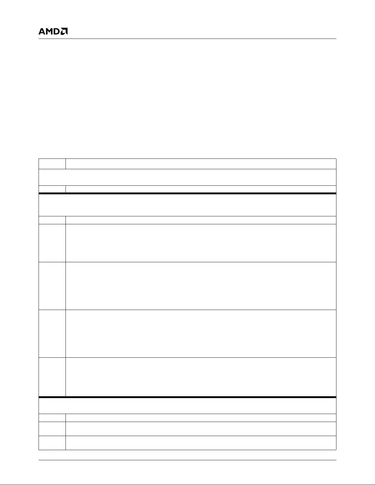
32580B
General Configuration Block
WATCHDOG Interrupt
The WATCHDOG interrupt (if configured and enabled) is
4.3.2 WATCHDOG Registers
Table 4-3 describes the WATCHDOG registers.
routed to an IRQ signal. The IRQ signal is programmable
via the INTSEL register (Offset 38h, described in Table 4-2
"Multiplexing, Interrupt Selection, and Base Address Regis-
ters" on page 76). The WATCHDOG interrupt is a shareable, active low, level interrupt.
WATCHDOG SMI
The WATCHDOG SMI is recognized by the Core Logic
module as internal input signal EXT_SMI0#. To use the
WATCHDOG SMI, Core Logic registers must be configured
appropriately.
4.3.2.1 Usage Hints
• SMM code should set bit 8 of the WDCNFG register to 1
when entering ACPI C3 state, if the WATCHDOG timer
is to be suspended. If this is not done, the WATCHDOG
timer is functional during C3 state.
• SMM code should set bit 8 of the WDCNFG register to
1, when entering ACPI S1 and S2 states if the
WATCHDOG timer is to be suspended. If this is not
done, the WATCHDOG timer is functional during S1 and
S2 states.
Table 4-3. WATCHDOG Registers
Bit Description
Offset 00h-01h WATCHDOG Timeout Register - WDTO (R/W) Reset Value: 0000h
This register specifies the programmed WATCHDOG timeout period.
15:0 Programmed timeout period.
Offset 02h-03h WATCHDOG Configuration Register - WDCNFG (R/W) Reset Value: 0000h
This register selects the signal to be generated when the timer reaches 0, whether or not to disable the 32 KHz input clock during low
power states, and the prescaler value of the clock input.
15:9 Reserved. Write as read.
8 WD32KPD (WATCHDOG 32 KHz Power Down).
0: 32 KHz clock is enabled.
1: 32 KHz clock is disabled, when the GX1 module asserts its internal SUSPA# signal.
This bit is cleared to 0, when POR# is asserted or when the GX1 module de-asserts its internal SUSPA# signal (i.e., on
SUSPA# rising edge). See Section 4.3.2.1 "Usage Hints" on page 84.
7:6 WDTYPE2 (WATCHDOG Event Type 2).
00: No action
01: Interrupt
10: SMI
11: System reset
This field is reset to 0 when POR# is asserted. Other system resets do not affect this field.
5:4 WDTYPE1 (WATCHDOG Event Type 1).
00: No action
01: Interrupt
10: SMI
11: System reset
This field is reset to 0 when POR# is asserted. Other system resets do not affect this field.
3:0 WDPRES (WATCHDOG Timer Prescaler). Divide 32 KHz by:
0000: 1 0100: 16 1000: 256 1100: 4096
0001: 2 0101: 32 1001: 512 1101: 8192
0010: 4 0110: 64 1010: 1024 1110: Reserved
0011: 8 0111: 128 1011: 2048 1111: Reserved
Offset 04h WATCHDOG Status Register - WDSTS (R/WC) Reset Value: 00h
This register contains WATCHDOG status information.
7:4 Reserved. Write as read.
3 WDRST (WATCHDOG Reset Asserted) (Read Only). This bit is set to 1 when WATCHDOG Reset is asserted. It is set to
0 when POR# is asserted, or when the WDOVF bit is set to 0.
2 WDSMI (WATCHDOG SMI Asserted.) (Read Only). This bit is set to 1 when WATCHDOG SMI is asserted. It is set to 0
when POR# is asserted, or when the WDOVF bit is set to 0.
84 AMD Geode™ SC2200 Processor Data Book
Page 81

General Configuration Block
32580B
Table 4-3. WATCHDOG Registers (Continued)
Bit Description
1 WDINT (WATCHDOG Interrupt Asserted, Read Only). This bit is set to 1 when the WATCHDOG Interrupt is asserted. It
is set to 0 when POR# is asserted, or when the WDOVF bit is set to 0.
0 WDOVF (WATCHDOG Overflow). This bit is set to 1 when the WATCHDOG Timer reaches 0. It is set to 0 when POR# is
asserted, or when a 1 is written to this bit by software. Other system reset sources do not affect this bit.
Offset 05h-07h Reserved - RSVD
4.4 High-Resolution Timer
The SC2200 provides an accurate time value that can be
used as a time stamp by system software. This time is
called the High-Resolution Timer. The length of the timer
value can be extended via software. It is normally enabled
while the system is in the C0 and C1 states. Optionally,
software can be programmed to enable use of the HighResolution Timer during C3 state and/or S1 state as well.
In all other power states the High-Resolution Timer is disabled.
4.4.1 Functional Description
The High-Resolution Timer is a 32-bit free-running countup timer that uses the oscillator clock or the oscillator clock
divided by 27. Bit TMCLKSEL of the TMCNFG register
(Offset 0Dh[1]) can be set via software to determine which
clock should be used for the High-Resolution Timer.
When the most significant bit (bit 31) of the timer changes
from 1 to 0, bit TMSTS of the TMSTS register (Offset
0Ch[0]) is set to 1. When both bit TMSTS and bit TMEN
(Offset 0Dh[0]) are 1, an interrupt is asserted. Otherwise,
the interrupt is de-asserted. This interrupt enables software
emulation of a larger timer.
The High-Resolution Timer interrupt is routed to an IRQ
signal. The IRQ signal is programmable via the INTSEL
register (Offset 38h). For more information about this register, see section Section 4.2 "Multiplexing, Interrupt Selection, and Base Address Registers" on page 76.
System software uses the read-only TMVALUE register
(Offset 08h[31:0]) to read the current value of the timer.
The TMVALUE register has no default value.
The input clock (derived from the 27 MHz crystal oscillator)
is enabled when:
The input clock is disabled, when the GX1 module’s internal SUSPA# signal is 0 and the TM27MPD bit is 1.
For more information about signal SUSPA# see Section
4.4.2.1 "Usage Hints" on page 85 and the AMD Geode™
GX1 Processor Data Book.
The High-Resolution Timer function resides on the internal
Fast-PCI bus and its registers are in General Configuration
Block address space. Only one complete register should
be accessed at-a-time (e.g., DWORD access should be
used for DWORD wide registers and byte access should be
used for byte-wide registers).
4.4.2 High-Resolution Timer Registers
Table 4-4 on page 86 describes the registers for the HighResolution Timer (TIMER).
4.4.2.1 Usage Hints
• SMM code should set bit 2 of the TMCNFG register to 1
when entering ACPI C3 state if the High-Resolution
Timer should be disabled. If this is not done, the HighResolution Timer is functional during C3 state.
• SMM code should set bit 2 of the TMCNFG register to 1
when entering ACPI S1 state if the High-Resolution
Timer should be disabled. If this is not done, the HighResolution Timer is functional during S1 state.
• The GX1 module’s internal SUSPA# signal is 1.
or
• The GX1 module’s internal SUSPA# signal is 0 and bit
TM27MPD (Offset 0Dh[2]) is 0.
AMD Geode™ SC2200 Processor Data Book 85
Page 82

32580B
General Configuration Block
Table 4-4. High-Resolution Timer Registers
Bit Description
Offset 08h-0Bh TIMER Value Register - TMVALUE (RO) Reset Value: xxxxxxxxh
This register contains the current value of the High-Resolution Timer.
31:0 Current Timer Value.
Offset 0Ch TIMER Status Register - TMSTS (R/W) Reset Value: 00h
This register supplies the High-Resolution Timer status information.
7:1 Reserved.
0 TMSTS (TIMER Status). This bit is set to 1 when the most significant bit (bit 31) of the timer changes from 1 to 0. It is
cleared to 0 upon system reset or when 1 is written by software to this bit.
Offset 0Dh TIMER Configuration Register - TMCNFG (R/W) Reset Value: 00h
This register enables the High-Resolution Timer interrupt; selects the Timer clock; and disables the 27 MHz internal clock during low
power states.
7:3 Reserved.
2 TM27MPD (TIMER 27 MHz Power Down). This bit is cleared to 0 when POR# is asserted or when the GX1 module de-
asserts its internal SUSPA# signal (i.e., on SUSPA# rising edge). See Section 4.4.2.1 "Usage Hints" on page 85.
0: 27 MHz input clock is enabled.
1: 27 MHz input clock is disabled when the GX1 module asserts its internal SUSPA# signal.
1 TMCLKSEL (TIMER Clock Select).
0: Count-up timer uses the oscillator clock divided by 27.
1: Count-up timer uses the oscillator clock, 27 MHz clock.
0 TMEN (TIMER Interrupt Enable).
0: High-Resolution Timer interrupt is disabled.
1: High-Resolution Timer interrupt is enabled.
Offset 0Eh-0Fh Reserved - RSVD
86 AMD Geode™ SC2200 Processor Data Book
Page 83
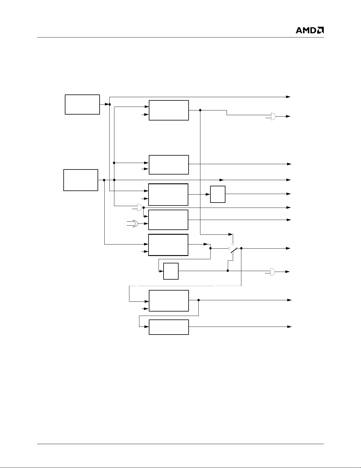
General Configuration Block
4.5 Clock Generators and PLLs
This section describes the registers for the clocks required
by the GX1 module, Core Logic module, and the Video
Processor, and how these clocks are generated. See Figure 4-2 for a clock generation diagram.
32580B
The clock generators are based on 32.768 KHz and 27.000
MHz crystal oscillators. The 32.768 KHz crystal oscillator is
described in Section 5.5.2 "RTC Clock Generation" on
page 111 (functional description of the RTC).
32.768 KHz
Crystal
Oscillator
27 MHz
Crystal
Oscillator
32.768 KHz
Shutdown
Shutdown
Shutdown
Shutdown
Shutdown
DISABLE
Shutdown
(ACPI)
PLL4
48 MHz
24.576 MHz
PLL6
57.273 MHz
CLK
PLL2
25-135 MHz
PLL5
66.67 MHz
Divide
PLL3
by 2
Divide
by 4
48 MHz
66 MHz
33 MHz
Real-Time Clock (RTC)
USB Clock (48 MHz)
and I/O Block Clock
DISABLE
AC97_CLK
(24.576 MHz)
High-Resolution Timer Clock
ACPI Clock (14.318 MHz)
CLK27M Ball
Dot Clock
Internal Fast-PCI Clock
External PCI Clock
(33.3 MHz)
DISABLE
To PA D
Core Clock
SDRAM Clock
Note: V
powers PLL2 and PLL5. V
PLL2
Shutdown
(ACPI)
ADL
100-333 MHz
Divider
powers PLL3, PLL4, and PLL6.
PLL3
Figure 4-2. Clock Generation Block Diagram
AMD Geode™ SC2200 Processor Data Book 87
Page 84
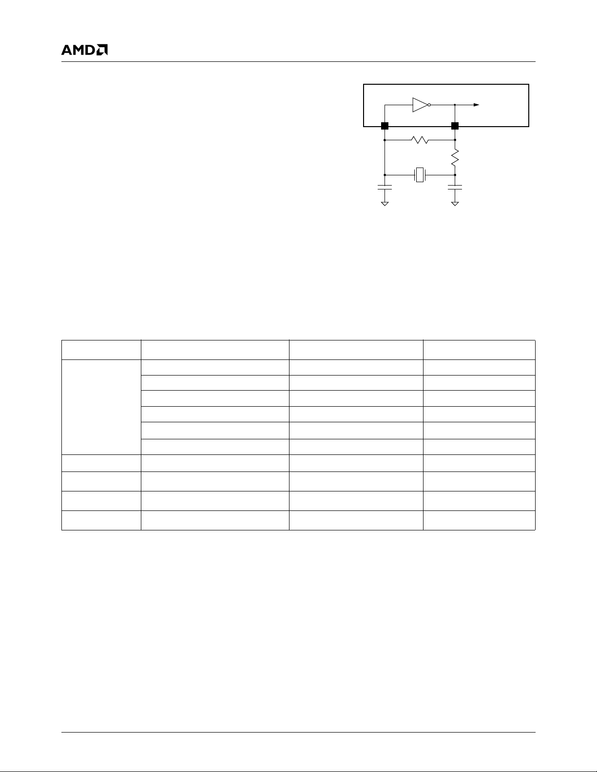
32580B
4.5.1 27 MHz Crystal Oscillator
The internal oscillator employs an external crystal connected to the on-chip amplifier. The on-chip amplifier is
accessible on the X27I input and X27O output signals. See
Figure 4-3 for the recommended external circuit and Table
4-5 for a list of the circuit components.
Choose C1 and C2 capacitors to match the crystal’s load
capacitance. The load capacitance CL “seen” by crystal Y
is comprised of C
in series with C2 and in parallel with the
1
parasitic capacitance of the circuit. The parasitic capacitance is caused by the chip package, board layout and
socket (if any), and can vary from 0 to 10 pF. The rule of
thumb in choosing these capacitors is:
= (C1 * C2) / (C1 + C2) + C
C
L
PARASITIC
Example 1:
Crystal CL = 10 pF, C
PARASITIC
= 8.2 pF
C1 = 3.6 pF, C2 = 3.6 pF
Example 2:
Crystal C
= 20 pF, C
L
PARASITIC
= 8 pF
C1 = 24 pF, C2 = 24 pF
Table 4-5. Crystal Oscillator Circuit Components
General Configuration Block
To other
modules
Internal
X27I
R
1
R
2
C
Y
1
X27O
C
2
External
Figure 4-3. Recommended Oscillator External
Circuitry
Component Parameters Values Tolerance
Crystal Resonance Frequency 27.00 MHz Parallel mode 50 PPM or better
Type AT-cut or BT-cut
Serial Resistance 40 Ω Max
Shunt Capacitance 7 pF Max
Load Capacitance, C
L
10-20 pF
Temperature Coefficient User-defined
Resistor R
Resistor R
Capacitor C
Capacitor C
1
1
2
1
2
Resistance 20 MΩ 5%
Resistance 100 Ω 5%
1
Capacitance 3-24 pF 5%
1
Capacitance 3-24 pF 5%
1. The value of these components is recommended. It should be tuned according to crystal and board parameters.
88 AMD Geode™ SC2200 Processor Data Book
Page 85
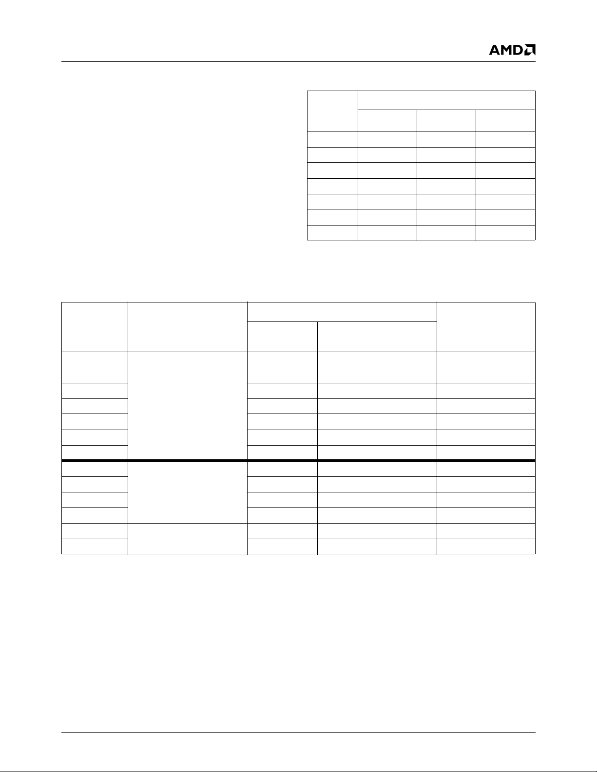
General Configuration Block
32580B
4.5.2 GX1 Module Core Clock
The core clock is generated by an Analog Delay Loop
(ADL) clock generator from the internal Fast-PCI clock. The
clock can be any whole-number multiple of the input clock
between 4 and 10. Possible values are listed in Table 4-6.
At power-on reset, the core clock multiplier value is set
according to the value of four strapped balls - CLKSEL[3:0]
(balls P30, D29, AF3, B8). These balls also select the clock
which is used as input to the multiplier, as shown in Table
4-7.
4.5.3 Internal Fast-PCI Clock
The internal Fast-PCI clock can be configured to 33, 48, or
66 MHz via strap options on the CLKSEL1 and CLKSEL0
balls. These can be read in the internal Fast-PCI Clock field
in the CCFC register (GCB+I/O Offset 1Eh[9:8]). (See
Table 4-9 on page 92 details on the CCFC register.)
Table 4-7. Strapped Core Clock Frequency
Internal Fast-PCI Clock
CLKSEL[3:0]
Straps
(GCB+I/O Offset 1Eh[9:8])
Freq. (MHz)
Multiply By
Table 4-6. Core Clock Frequency
ADL
Multiplier
Val ue
4 133.3 192 266.7
5 166.7 240 ---
6 200 288 ---
7 233.3 --- ---
8 266.7 --- ---
9 300 --- ---
10 --- --- ---
Default ADL Multiplier
(GCB+I/O Offset 1Eh[3:0])
Internal Fast-PCI Clock Freq. (MHz)
33.33 48 66.67
Multiplier Value
Maximum Core
Clock Freq. (MHz)
0111 33.33 4 0100 133
1011 5 0101 167
1111 6 0110 200
0000 7 0111 233
0100 8 1000 266
1000 9 1001 300
1100 10 1010 Reserved
0001 48 4 0100 192
0101 5 0101 240
1001 6 0110 288
1101 7 0111 Reserved
0110 66.67 4 0100 266
1010 5 0101 Reserved
Note: Not all speeds are supported. For information on supported speeds, see Section A.1 "Order Information" on page
447.
AMD Geode™ SC2200 Processor Data Book 89
Page 86

32580B
General Configuration Block
4.5.4 SuperI/O Clocks
The SuperI/O module requires a 48 MHz input for Fast
infrared (FIR), UART, and other functions. This clock is supplied by PLL4 using a multiplier value of 576/(108x3) to
generate 48 MHz.
4.5.5 Core Logic Module Clocks
The Core Logic module requires the following clock
sources:
Real-Time Clock (RTC)
RTC requires a 32.768 KHz clock which is supplied directly
from an internal low-power crystal oscillator. This oscillator
uses battery power and has very low current consumption.
USB
The USB requires a 48 MHz input which is supplied by
PLL4. The required total frequency accuracy and slow jitter
for USB is 500 PPM; edge to edge jitter is ±1.2%.
ACPI
The ACPI logic block uses a 14.32 MHz clock supplied by
PLL6. PLL6 creates this clock from the 32.768 KHz clock,
with a multiplier value of 6992/4 to output a 57.278 MHz
clock that is divided by 4.
4.5.6 Video Processor Clocks
The Video processor requires the following clock sources:
Dot
The Dot clock is generated by PLL2. It is supplied to the
Display Controller in the GX1 module (DCLK) that creates
the pixel information, and is returned to the Graphics block
(PCLK) with this information. PLL2 uses the 27 MHz clock
to generate the Dot clock.
Video
The Video clock source depends on the source of the video
data.
• If the video data is coming from the GX1 module
(Capture Video mode), the video clock is generated by
the Display Controller.
• If the video data is coming directly from the VIP block
(Direct Video mode), the Video Clock is generated by
the VIP block.
External PCI
The PCI Interface uses a 33.3 MHz clock that is created by
PLL5 and divided by 2. PLL5 uses the 27 MHz clock, to
output a 66.67 MHz clock. PLL5 has a frequency accuracy
of ± 0.1%.
AC97
The SC2200 generates the 24.576 MHz clock required by
the audio codec. Therefore, no crystal need be included for
the audio codec on the system board.
PLL3 uses the crystal oscillator clock, to generate a 24.576
MHz clock. This clock is driven on the AC97_CLK ball. The
accuracy of the clock supplied by the SC2200 is 50 PPM.
90 AMD Geode™ SC2200 Processor Data Book
Page 87
General Configuration Block
32580B
4.5.7 Clock Registers
Table 4-9 describes the registers of the clock generator and PLL.
Table 4-8. Clock Generator Configuration
Bit Description
Offset 10h Maximum Core Clock Multiplier Register - MCCM (RO) Reset Value: Strapped Value
This register holds the maximum core clock multiplier value. The maximum clock frequency allowed by the core, is the Fast-PCI clock
multiplied by this value.
7:4 Reserved.
3:0 MCM (Maximum Clock Multiplier). This 4-bit value is the maximum multiplier value allowed for the core clock generator. It
Offset 11h Reserved - RSVD
Offset 12h PLL Power Control Register - PPCR (R/W) Reset Value: 2Fh
This register controls operation of the PLLs.
Offset 13h-17h Reserved - RSVD
is derived from strap pins CLKSEL[3:0] based on the multiplier value in Table 4-7 on page 89.
7 Reserved.
6 EXPCID (Disable External PCI Clock).
0: External PCI clock is enabled.
1: External PCI clock is disabled.
5 GPD (Disable Graphic Pixel Reference Clock).
0: PLL2 input clock is enabled.
1: PLL2 input clock is disabled.
4 Reserved.
3 PLL3SD (Shut Down PLL3). AC97 codec clock.
0: PLL3 is enabled.
1: PLL3 is shutdown.
2 FM1SD (Shut Down PLL4).
0: PLL4 is enabled.
1: PLL4 is shutdown, unless internal Fast-PCI clock is strapped to 48 MHz.
1 C48MD (Disable SuperI/O and USB Clock).
0: USB and SuperI/O clock is enabled.
1: USB and SuperI/O clock is disabled.
0 Reserved. Write as read.
Offset 18h-1Bh PLL3 Configuration Register - PLL3C (R/W) Reset Value: E1040005h
31:24 MFFC (MFF Counter Value).
Fvco = OSCCLK * MFBC / (MFFC * MOC)
OSCCLK = 27 MHz
23:19 Reserved. Write as read.
18:8 MFBC (MFB Counter Value).
Fvco = OSCCLK * MFBC / (MFFC * MOC)
OSCCLK = 27 MHz
Note: Bits 18, 9, and 8 cannot be changed. Bit 18 is always a 1; bits 9 and 8 are always 0.
7 Reserved. Write as read.
6 Reserved. Must be set to 0.
5:0 MOC (MO Counter Value).
Fvco = OSCCLK * MFBC / (MFFC * MOC)
OSCCLK = 27 MHz
Offset 1Eh-1Fh Core Clock Frequency Control Register - CCFC (R/W) Reset Value: Strapped Value
This register controls the configuration of the core clock multiplier and the reference clocks.
AMD Geode™ SC2200 Processor Data Book 91
Page 88

32580B
General Configuration Block
Table 4-8. Clock Generator Configuration (Continued)
Bit Description
15:14 Reserved.
13 Reserved. Must be set to 0.
12 Reserved. Must be set to 0.
11:10 Reserved.
9:8 FPCICK (Internal Fast-PCI Clock). (Read Only) Reflects the internal Fast-PCI clock and is the input to the GX1 module
7:4 Reserved.
3:0 MVAL (Multiplier Value). This 4-bit value controls the multiplier in ADL. The value is set according to the Maximum Clock
that is used to generate the core clock. These bits reflect the value of strap pins CLKSEL[1:0].
00: 33.3 MHz
01: 48 MHz
10: 66.7 MHz
11: 33.3 MHz
Multiplier bits of the MCCM register (Offset 10h). The multiplier value should never be written with a multiplier which is different from the multiplier indicated in the MCCM register.
0100: Multiply by 4
0101: Multiply by 5
0110: Multiply by 6
0111: Multiply by 7
1000: Multiply by 8
1001: Multiply by 9
1010: Multiply by 10
Other: Reserved
92 AMD Geode™ SC2200 Processor Data Book
Page 89
SuperI/O Module 32580B
5.0SuperI/O Module
5
The SuperI/O (SIO) module is PC98 and ACPI compliant. It
offers a single-cell solution to the most commonly used ISA
peripherals.
The SIO module incorporates: two Serial Ports, an Infrared
Communication Port that supports FIR, MIR, HP-SIR,
Sharp-IR, and Consumer Electronics-IR, a full IEEE 1284
Parallel Port, two ACCESS.bus Interface (ACB) ports, System Wakeup Control (SWC), and a Real-Time Clock (RTC)
that provides RTC timekeeping.
Serial
Interface
Serial Port 1
System Wakeup
Control
Serial
Interface
Serial Port 2
Infrared /Serial
Interface
IR Comunication
Port/Serial Port 3
ACCESS.bus 1
Outstanding Features
• Full compatibility with ACPI Revision 1.0 requirements.
• System Wakeup Control powered by V
power-up request and a PME (power management
event) in response to SDATA_IN2 (an audio codec),
IRRX1 (a pre-programmed CEIR), or a RI2# (Serial Port
ring indicate) event.
• Advanced RTC, Y2K compliant.
V
Real-Time Clock
ACCESS.bus 2
BAT
V
SB
IEEE 1284
Parallel Por t
, generates
SB
ISA
Interface
Host Interface
Wakeup
Events
AMD Geode™ SC2200 Processor Data Book 95
AB1DAB1C
Figure 5-1. SIO Block Diagram
AB2C
AB2DPWUREQ
Parallel Por t
Interface
Page 90

5.1 Features
32580B
SuperI/O Module
PC98 and ACPI Compliant
• PnP Configuration Register structure
• Flexible resource allocation for all logical devices:
— Relocatable base address
— 9 parallel IRQ routing options
— 3 optional 8-bit DMA channels (where applicable)
Parallel Port
• Software or hardware control
• Enhanced Parallel Port (EPP) compatible with version
EPP 1.9 and IEEE 1284 compliant
• EPP support for version EPP 1.7 of the Xircom specification
• EPP support as mode 4 of the Extended Capabilities
Por t (EC P)
• IEEE 1284 compliant ECP, including level 2
• Selection of internal pull-up or pull-down resistor for
Paper End (PE) pin
• PCI bus utilization reduction by supporting a demand
DMA mode mechanism and a DMA fairness mechanism
• Protection circuit that prevents damage to the Parallel
Port when a printer connected to it powers up or is operated at high voltages, even if the device is in powerdown
• Output buffers that can sink and source 14 mA
Serial Port 1
• 16550A compatible (SIN1, SOUT1, DTR1#/BOUT1
signals only)
Serial Port 2
• 16550A compatible
Serial Port 3 / Infrared (IR) Communication Port
• Serial Port 3
— SIN and SOUT signals only
— Data rate of up to 1.5 Mbps
— Software compatible with the 16550A and the 16450
— Shadow register support for write-only bit monitoring
— DMA support
• IR Communication Port
— IrDA 1.1 and 1.0 compatible
— Data rate of up to 115.2 Kbps (HP-SIR)
— Data rate of 1.152 Mbps (MIR)
— Data rate of 4.0 Mbps (FIR)
— Selectable internal or external modulation/demodula-
tion (ASK-IR and DASK-IR options of SHARP-IR)
— Consumer-IR (TV-Remote) mode
— Consumer Remote Control supports RC-5, RC-6,
NEC, RCA and RECS 80
— DMA support
System Wakeup Control (SWC)
• Power-up request upon detection of RI2#, CEIR, or
SDATA_IN2 activity:
— Optional routing of power-up request on IRQ line
• Pre-programmed CEIR address in a pre-selected
standard (any NEC, RCA or RC-5)
• Powered by V
SB
• Battery-backed wakeup setup
• Power-fail recovery support
Real-Time Clock
• A modifiable address that is referenced by a 16-bit
programmable register
• DS1287, MC146818 and PC87911 compatibility
• 242 bytes of battery backed up CMOS RAM in two
banks
• Selective lock mechanisms for the CMOS RAM
• Battery backed up century calendar in days, day of the
week, date of month, months, years and century, with
automatic leap-year adjustment
• Battery backed-up time of day in seconds, minutes and
hours that allows a 12 or 24 hour format and adjustments for daylight savings time
• BCD or binary format for time keeping
• Three different maskable interrupt flags:
— Periodic interrupts - At intervals from 122 msec to
500 msec
— Time-of-Month alarm - At intervals from once per
second to once per month
— Update Ended Interrupt - Once per second upon
completion of update
• Separate battery pin, 3.0V operation that includes an
internal UL protection resistor
• 7 µA typical power consumption during power down
• Double-buffer time registers
• Y2K Compliant
Clock Sources
• 48 MHz clock input
• On-chip low frequency clock generator for wakeup
• 32.768 KHz crystal with an internal frequency multiplier
to generate all required internal frequencies
96 AMD Geode™ SC2200 Processor Data Book
Page 91

SuperI/O Module
5.2 Module Architecture
The SIO module comprises a collection of generic functional blocks. Each functional block is described in detail
later in this chapter. The beginning of this chapter
describes the SIO structure and provides all device specific
information, including special implementation of generic
blocks, system interface and device configuration.
The SIO module is based on eight logical devices, the host
interface, and a central configuration register set, all built
around a central, internal 8-bit bus.
The host interface serves as a bridge between the external
ISA interface and the internal bus. It supports 8-bit I/O
read, 8-bit I/O write and 8-bit DMA transactions, as defined
in Personal Computer Bus Standard P996.
32580B
The central configuration register set supports ACPI compliant PnP configuration. The configuration registers are
structured as a subset of the Plug and Play Standard Registers, defined in Appendix A of the Plug and Play ISA
Specification Version 1.0a by Intel and Microsoft
®
. All system resources assigned to the functional blocks (I/O
address space, DMA channels and IRQ lines) are configured in, and managed by, the central configuration register
set. In addition, some function-specific parameters are configurable through this unit and distributed to the functional
blocks through special control signals.
The source of the device internal clocks is the 48 MHz
clock signal or through the 32.768 KHz crystal with an
internal frequency multiplier. RTC operates on a 32 KHz
clock.
AFD#/DSTRB#
ACK#
BUSY/WAIT#
ERR#
INIT#
PD[7:0]
PE
SLCT
SLIN#/ASTRB#
STB#/WRITE#
AB1C
AB1D
AB2C
AB2D
Real-Time Clock (RTC)
Parallel
Por t
ACCESS.
bus 1
ACCESS.
bus 2
IRTX/SOUT3
Infrared
Communication
Port/Serial Port 3
Configuration
and Control
Registers
System
Wakeup
IRRX1/SIN3
Serial
Por t 1
Serial
Por t 2
Internal
Host
Interface
SIN1
SOUT1
DTR#/BOUT1
SIN2
SOUT2
RTS2#
DTR2#/BOUT2
CTS2
RI2#
DCD2#
DSR2#
TC
DACK0-3
DRQ0-3
IRQ1-12,14-15
IOCHRDY
ZWS#
IOWR#
IORD#
AEN
Internal
Signals
SB
ALARM
Internal
Signal
X2C
X1C/X1
BAT
V
V
Internal Bus
Control Signals
RI2#
PWUREQ
SDATA_IN2
Internal Signals
CONFIG
MR
CLKIN
D[7:0]
A[15:0]
Figure 5-2. Detailed SIO Block Diagram
AMD Geode™ SC2200 Processor Data Book 97
Page 92

32580B
SuperI/O Module
5.3 Configuration Structure/Access
This section describes the structure of the configuration
register file, and the method of accessing the configuration
registers.
5.3.1 Index-Data Register Pair
The SIO configuration access is performed via an IndexData register pair, using only two system I/O byte locations.
The base address of this register pair is determined
according to the state of the IO_SIOCFG_IN bit field of the
Core Logic module (F5BAR0+I/O Offset 00h[26:25]). Table
5-1 shows the selected base addresses as a function of the
IO_SIOCFG_IN bit field.
Table 5-1. SIO Configuration Options
I/O Address
IO_SIOCFG_IN
Settings
00 - - SIO disabled
01 - - Configuration
10 002Eh 002Fh Base address 1
11 015Ch 015Dh Base address 2
The Index Register is an 8-bit R/W register located at the
selected base address (Base+0). It is used as a pointer to
the configuration register file, and holds the index of the
configuration register that is currently accessible via the
Data Register. Reading the Index Register returns the last
value written to it (or the default of 00h after reset).
The Data Register is an 8-bit virtual register, used as a
data path to any configuration register. Accessing the data
register results with physically accessing the configuration
register that is currently pointed by the Index Register.
5.3.2 Banked Logical Device Registers
Each functional block is associated with a Logical Device
Number (LDN). The configuration registers are grouped
into banks, where each bank holds the standard configuration registers of the corresponding logical device. Table 5-2
shows the LDNs of the device functional blocks.
Index
Register
Data
Register
Description
access disabled
selected
selected
Table 5-2. LDN Assignments
LDN Functional Block Reference
00h Real-Time Clock (RTC) Page 104
01h System Wakeup Control (SWC) Page 106
02h Infrared Communication Port
(IRCP) or Serial Port 3 (SP3)
03h Serial Port 1 (SP1) Page 108
05h ACCESS.bus 1 (ACB1) Page 109
06h ACCESS.bus 2 (ACB2)
07h Parallel Port (PP) Page 110
08h Serial Port 2 (SP2) Page 108
Figure 5-3 shows the structure of the standard PnP configuration register file. The SIO Control And Configuration
registers are not banked and are accessed by the IndexData register pair only (as described above). However, the
Logical Device Control and Configuration registers are
duplicated over eight banks for eight logical devices. Therefore, accessing a specific register in a specific bank is performed by two-dimensional indexing, where the LDN
register selects the bank (or logical device), and the Index
register selects the register within the bank. Accessing the
Data register while the Index register holds a value of 30h
or higher results in a physical access to the Logical Device
Configuration registers currently pointed to by the Index
register, within the logical device bank currently selected by
the LDN register.
07h
20h
2Fh
30h
60h
63h
70h
71h
74h
75h
F0h
FEh
Logical Device Number Register
SIO Configuration Registers
Logical Device Control Register
Standard Logical Device
Standard Registers
Special (Vendor-defined)
Logical Device
Configuration Registers
Page 107
Bank
Select
Banks
(One per Logical Device)
Figure 5-3. Structure of the Standard
Configuration Register File
98 AMD Geode™ SC2200 Processor Data Book
Page 93

SuperI/O Module
32580B
Write accesses to unimplemented registers (i.e., accessing
the Data register while the Index register points to a nonexisting register or the LDN is 07h or higher than 08h), are
ignored and a read returns 00h on all addresses except for
74h and 75h (DMA configuration registers) which returns
04h (indicating no DMA channel is active). The configuration registers are accessible immediately after reset.
5.3.3 Default Configuration Setup
The device has four reset types:
Software Reset
This reset is generated by bit 1 of the SIOCF1 register,
which resets all logical devices. A software reset also
resets most bits in the SIO Configuration and Control registers (see Section 5.4.1 on page 103 for the bits not
affected). This reset does not affect register bits that are
locked for write access.
Hardware Reset
This reset is activated by the system reset signal. This
resets all logical devices, with the exception of the RTC and
the SWC, and all SIO Configuration and Control registers,
with the exception of the SIOCF2 register. It also resets all
SuperI/O control and configuration registers, except for
those that are battery-backed.
Power-Up Reset
V
PP
This reset is activated when either VSB or V
on after both have been off. VPP is an internal voltage
which is a combination of V
and V
SB
. VPP is taken from
BAT
VSB if VSB is greater than the minimum (Min) value defined
in Section 9.1.4 "Operating Conditions" on page 370; otherwise, V
is used as the VPP source. This reset resets
BAT
all registers whose values are retained by V
VSB Power-Up Reset
This is an internally generated reset that resets the SWC,
excluding those SWC registers whose values are retained
. This reset is activated after VSB is powered up.
by V
PP
The SIO module wakes up with the default setup, as follows:
BAT
PP.
is powered
• When a hardware reset occurs:
— The configuration base address is 2Eh, 15Ch or
None, according to the IO_SIOCFG_IN bit values, as
shown in Table 5-1 on page 98.
— All Logical devices are disabled, with the exception of
the RTC and the SWC, which remains functional but
whose registers cannot be accessed.
• When either a hardware or a software reset occurs:
— The legacy devices are assigned with their legacy
system resource allocation.
— The AMD proprietary functions are not assigned with
any default resources and the default values of their
base addresses are all 00h.
5.3.4 Address Decoding
A full 16-bit address decoding is applied when accessing
the configuration I/O space, as well as the registers of the
functional blocks. However, the number of configurable bits in
the base address registers vary for each device.
The lower 1, 2, 3 or 4 address bits are decoded within the
functional block to determine the offset of the accessed
register, within the device’s I/O range of 2, 4, 8 or 16 bytes,
respectively. The rest of the bits are matched with the base
address register to decode the entire I/O range allocated to
the device. Therefore the lower bits of the base address
register are forced to 0 (RO), and the base address is
forced to be 2, 4, 8 or 16 byte aligned, according to the size
of the I/O range.
The base address of the RTC, Serial Port 1, Serial Port 2,
and the Infrared Communication Port are limited to the I/O
address range of 00h to 7Fxh only (bits [15:11] are forced
to 0). The Parallel Port base address is limited to the I/O
address range of 00h to 3F8h. The addresses of the nonlegacy devices are configurable within the full 16-bit
address range (up to FFFxh).
In some special cases, other address bits are used for
internal decoding (such as 10 in the Parallel Port). For
more details, please see the detailed description of the
base address register for each specific logical device.
AMD Geode™ SC2200 Processor Data Book 99
Page 94

32580B
SuperI/O Module
5.4 Standard Configuration Registers
As illustrated in Figure 5-4, the Standard Configuration registers are broadly divided into two categories: SIO Control
and Configuration registers and Logical Device Control and
Configuration registers (one per logical device, some are
optional).
SIO Control and Configuration Registers
The only PnP control register in the SIO module is the Logical Device Number register at Index 07h. All other standard PnP control registers are associated with PnP
protocol for ISA add-in cards, and are not supported by the
SIO module.
The SIO Configuration registers at Index 20h-27h are
mainly used for part identification. (See Section 5.4.1 "SIO
Control and Configuration Registers" on page 103 for further details.)
Logical Device Control and Configuration Registers
A subset of these registers is implemented for each logical
device. (See Table 5-2 on page 98 for LDN assignment and
Section 5.4.2 "Logical Device Control and Configuration"
on page 104 for register details.)
Logical Device Control Register (Index 30h): The only
implemented Logical Device Control register is the Activate
register at Index 30. Bit 0 of the Activate register and bit 0
of the SIO Configuration 1 register (Global Device Enable
bit) control the activation of the associated function block
Index Register Name
07h Logical Device Number
20h SIO ID
SIO Control and
Configuration Registers
Logical Device Control and
Configuration Registers one per logical device
(some are optional)
21h SIO Configuration 1
22h SIO Configuration 2
27h SIO Revision ID
2Eh Reserved exclusively for AMD use
30h Logical Device Control (Activate)
60h I/O Port Base Address Descriptor 0 Bits [15:8]
61h I/O Port Base Address Descriptor 0 Bits [7:0]
62h I/O Port Base Address Descriptor 1 Bits [15:8]
63h I/O Port Base Address Descriptor 1 Bits [7:0]
70h Interrupt Number Select
71h Interrupt Type Select
74h DMA Channel Select 0
75h DMA Channel Select 1
F0h Device Specific Logical Device Configuration 1
F1h Device Specific Logical Device Configuration 2
F2h Device Specific Logical Device Configuration 3
F3h Device Specific Logical Device Configuration 4
(except for the RTC and the SWC). Activation of the block
enables access to the block’s registers, and attaches its
system resources, which are unused as long as the block is
not activated. Activation of the block may also result in
other effects (e.g., clock enable and active signaling), for
certain functions.
Standard Logical Device Configuration Registers
(Index 60h-75h): These registers are used to manage the
resource allocation to the functional blocks. The I/O port
base address descriptor 0 is a pair of registers at Index
60h-61h, holding the (first or only) 16-bit base address for
the register set of the functional block. An optional second
base-address (descriptor 1) at Index 62h-63h is used for
devices with more than one continuous register set. Interrupt Number Select (Index 70h) and Interrupt Type Select
(Index 71h) allocate an IRQ line to the block and control its
type. DMA Channel Select 0 (Index 74h) allocates a DMA
channel to the block, where applicable. DMA Channel
Select 1 (Index 75h) allocates a second DMA channel,
where applicable.
Special Logical Device Configuration Registers (F0hF3h): The vendor-defined registers, starting at Index F0h
are used to control function-specific parameters such as
operation modes, power saving modes, pin TRI-STATE,
clock rate selection, and non-standard extensions to
generic functions.
Figure 5-4. Standard Configuration Registers Map
100 AMD Geode™ SC2200 Processor Data Book
Page 95

SuperI/O Module
32580B
Table 5-3 provides the bit definitions for the Standard Configuration registers.
• All reserved bits return 0 on reads, except where noted
otherwise. They must not be modified as such modifica-
write to prevent the values of reserved bits from being
changed during write.
• Write only registers should not use read-modify-write
during updates.
tion may cause unpredictable results. Use read-modify-
Table 5-3. Standard Configuration Registers
Bit Description
Index 07h Logical Device Number (R/W)
This register selects the current logical device. See Table 5-2 for valid numbers. All other values are reserved.
7:0 Logical Device number.
Index 20h-2Fh SIO Configuration (R/W)
SIO configuration and ID registers. See Section 5.4.1 "SIO Control and Configuration Registers" on page 103 for register/bit details.
Index 30h Activate (R/W)
7:1 Reserved.
0 Logical Device Activation Control.
0: Disable.
1: Enable.
Index 60h I/O Port Base Address Bits [15:8] Descriptor 0 (R/W)
7:0 Descriptor 0 A[15:8]. Selects I/O lower limit address bits [15:8] for I/O Descriptor 0.
Index 61h I/O Port Base Address Bits [7:0] Descriptor 0 (R/W)
7:0 Descriptor 0 A[7:0]. Selects I/O lower limit address bits [7:0] for I/O Descriptor 0.
Index 62h I/O Port Base Address Bits [15:8] Descriptor 1 (R/W)
7:0 Descriptor 1 A[15:8]. Selects I/O lower limit address bits [15:8] for I/O Descriptor 1.
Index 63h I/O Port Base Address Bits [7:0] Descriptor 1 (R/W)
7:0 Descriptor 1 A[7:0]. Selects I/O lower limit address bits [7:0] for I/O Descriptor 1.
Index 70h Interrupt Number (R/W)
7:4 Reserved.
3:0 Interrupt Number. These bits select the interrupt number. A value of 1 selects IRQ1, a value of 2 selects IRQ2, etc. (up to
Index 71h Interrupt Request Type Select (R/W)
Selects the type and level of the interrupt request number selected in the previous register.
7:2 Reserved.
Index 74h DMA Channel Select 0 (R/W)
Selects selected DMA channel for DMA 0 of the logical device (0 - the first DMA channel in case of using more than one DMA channel).
7:3 Reserved.
2:0 DMA 0 Channel Select. This bit field selects the DMA channel for DMA 0.
IRQ12).
Note: IRQ0 is not a valid interrupt selection.
1 Interrupt Level Requested. Level of interrupt request selected in previous register.
0: Low polarity.
1: High polarity.
This bit must be set to 1 (high polarity), except for IRQ8#, that must be low polarity.
0 Interrupt Type Requested. Type of interrupt request selected in previous register.
0: Edge.
1: Level.
The valid choices are 0-3, where a value of 0 selects DMA channel 0, 1 selects channel 1, etc.
A value of 4 indicates that no DMA channel is active.
Values 5-7 are reserved.
AMD Geode™ SC2200 Processor Data Book 101
Page 96
32580B
SuperI/O Module
Table 5-3. Standard Configuration Registers
Bit Description
Index 75h DMA Channel Select 1 (R/W)
Indicates selected DMA channel for DMA 1 of the logical device (1 - the second DMA channel in case of using more than one DMA
channel).
7:3 Reserved.
2:0 DMA 1 Channel Select: This bit field selects the DMA channel for DMA 1.
The valid choices are 0-3, where a value of 0 selects DMA channel 0, 1 selects channel 1, etc.
A value of 4 indicates that no DMA channel is active.
Values 5-7 are reserved.
Index F0h-FEh Logical Device Configuration (R/W)
Special (vendor-defined) configuration options.
102 AMD Geode™ SC2200 Processor Data Book
Page 97
SuperI/O Module
32580B
5.4.1 SIO Control and Configuration Registers
Table 5-4 lists the SIO Control and Configuration registers and Table 5-5 provides their bit formats.
Table 5-4. SIO Control and Configuration Register Map
Index Type Name Power Rail Reset Value
20h RO SID. SIO ID V
21h R/W SIOCF1. SIO Configuration 1 V
22h R/W SIOCF2. SIO Configuration 2 V
27h RO SRID. SIO Revision ID V
CORE
CORE
PP
CORE
F5h
01h
02h
01h
2Eh --- RSVD. Reserved exclusively for AMD use --- ---
Table 5-5. SIO Control and Configuration Registers
Bit Description
Index 20h SIO ID Register - SID (RO) Reset Value: F5h
7:0 Chip ID. Contains the identity number of the module. The SIO module is identified by the value F5h.
Index 21h SIO Configuration 1 Register - SIOCF1 (RW) Reset Value: 01h
7:6 General Purpose Scratch. When bit 5 is set to 1, these bits are RO. After reset, these bits can be read or write. Once
changed to RO, the bits can be changed back to R/W only by a hardware reset.
5 Lock Scratch. This bit controls bits 7 and 6 of this register. Once this bit is set to 1 by software, it can be cleared to 0 only
by a hardware reset.
0: Bits 7 and 6 of this register are R/W bits. (Default)
1: Bits 7 and 6 of this register are RO bits.
4:2 Reserved.
1 SW Reset. Read always returns 0.
0: Ignored. (Default)
1: Resets all devices that are reset by MR (with the exception of the lock bits) and the registers of the SWC.
0 Global Device Enable. This bit controls the function enable of all the logical devices in the SIO module, except the SWC
and the RTC. It allows them to be disabled simultaneously by writing to a single bit.
0: All logical devices in the SIO module are disabled, except the SWC and the RTC.
1: Each logical device is enabled according to its Activate register at Index 30h. (Default)
Index 22h SIO Configuration 2 Register - SIOCF2 (R/W) Reset Value: 02h
Note: This register is reset only when V
7 Reserved.
6:4 General Purpose Scratch. Battery-backed.
3:2 Reserved.
1 Reserved.
0 Reserved. (RO)
Index 27h SIO Revision ID Register - SRID (RO) Reset Value: 01h
7:0 SIO Revision ID. (RO) This RO register contains the identity number of the chip revision. SRID is incremented on each revi-
sion.
is first applied.
PP
AMD Geode™ SC2200 Processor Data Book 103
Page 98
32580B
SuperI/O Module
5.4.2 Logical Device Control and Configuration
As described in Section 5.3.2 "Banked Logical Device Registers" on page 98, each functional block is associated with
a Logical Device Number (LDN). This section provides the
register descriptions for each LDN.
5.4.2.1 LDN 00h - Real-Time Clock
Table 5-6 lists the registers which are relevant to configuration of the Real-Time Clock (RTC). Only the last registers
(F0h-F3h) are described here (Table 5-7). See Table 5-3
"Standard Configuration Registers" on page 101 for
descriptions of the other registers.
The register descriptions in this subsection use the following abbreviations for Type:
• R/W = Read/Write
• R = Read from a specific address returns the
value of a specific register. Write to the
same address is to a different register.
•W =Write
• RO = Read Only
• R/W1C = Read/Write 1 to Clear. Writing 1 to a bit
clears it to 0. Writing 0 has no effect.
Table 5-6. Relevant RTC Configuration Registers
Index Type Configuration Register or Action
30h R/W
Activate. When bit 0 is cleared, the registers of this logical device are not accessible.
60h R/W Standard Base Address MSB register. Bits [7:3] (for A[15:11]) are RO, 00000b. 00h
61h R/W Standard Base Address LSB register. Bit 0 (for A0) is RO, 0b. 70h
62h R/W Extended Base Address MSB register. Bits [7:3] (for A[15:11]) are RO, 00000b. 00h
63h R/W Extended Base Address LSB register. Bit 0 (for A0) is RO, 0b. 72h
70h R/W Interrupt Number. 08h
71h R/W Interrupt Type. Bit 1 is R/W; other bits are RO. 00h
74h RO Report no DMA assignment. 04h
75h RO Report no DMA assignment. 04h
F0h R/W RAM Lock register (RLR). 00h
F1h R/W Date of Month Alarm Offset register (DOMAO). Sets index of Date of Month Alarm
register in the standard base address.
F2h R/W Month Alarm Offset register (MONAO). Sets index of Month Alarm register in the
standard base address.
F3h R/W Century Offset register (CENO). Sets index of Century register in the standard base
address.
1. The logical device registers are maintained, and all RTC mechanisms are functional.
1
Reset
Val ue
00h
00h
00h
00h
104 AMD Geode™ SC2200 Processor Data Book
Page 99
SuperI/O Module
Table 5-7. RTC Configuration Registers
Bit Description
Index F0h RAM Lock Register - RLR (R/W)
When any non-reserved bit in this register is set to 1, it can be cleared only by hardware reset.
7 Block Standard RAM.
0: No effect on Standard RAM access. (Default)
1: Read and write to locations 38h-3Fh of the Standard RAM are blocked, writes ignored, and reads return FFh.
6 Block RAM Write.
0: No effect on RAM access. (Default)
1: Writes to RAM (Standard and Extended) are ignored.
5 Block Extended RAM Write. This bit controls writes to bytes 00h-1Fh of the Extended RAM.
0: No effect on the Extended RAM access. (Default)
1: Writes to bytes 00h-1Fh of the Extended RAM are ignored.
4 Block Extended RAM Read. This bit controls read from bytes 00h-1Fh of the Extended RAM.
0: No effect on Extended RAM access. (Default)
1: Reads to bytes 00h-1Fh of the Extended RAM are ignored.
3 Block Extended RAM. This bit controls access to the Extended RAM 128 bytes.
0: No effect on Extended RAM access. (Default)
1: Read and write to the Extended RAM are blocked: writes are ignored and reads return FFh.
2:0 Reserved.
Index F1h Date Of Month Alarm Register Offset Register - DOMAO (R/W)
7 Reserved.
6:0 Date of Month Alarm Register Offset Value.
Index F2h Month Alarm Register Offset Register - MANAO (R/W)
7 Reserved.
6:0 Month Alarm Register Offset Value.
Index F3h Century Register Offset Register - CENO (R/W)
7 Reserved.
6:0 Century Register Offset Value.
32580B
AMD Geode™ SC2200 Processor Data Book 105
Page 100

32580B
SuperI/O Module
5.4.2.2 LDN 01h - System Wakeup Control
Table 5-8 lists registers that are relevant to the configura-
described earlier in Table 5-3 "Standard Configuration Registers" on page 101.
tion of System Wakeup Control (SWC). These registers are
Table 5-8. Relevant SWC Registers
Index Type Configuration Register or Action
30h R/W
Activate. When bit 0 is cleared, the registers of this logical device are not accessible.
60h R/W Base Address MSB register. 00h
61h R/W Base Address LSB register. Bits [3:0] (for A[3:0]) are RO, 0000b. 00h
70h R/W Interrupt Number. (For routing the internal PWUREQ signal.) 00h
71h R/W Interrupt Type. Bit 1 is R/W. Other bits are RO. 03h
74h RO Report no DMA assignment. 04h
75h RO Report no DMA assignment. 04h
1. The logical device registers are maintained, and all wakeup detection mechanisms are functional.
1
Reset
Val ue
00h
106 AMD Geode™ SC2200 Processor Data Book
 Loading...