

Page 1

AMD SB600
Register Reference
(Public Version)
Technical Reference Manual
©2008 Advanced Micro Devices, Inc.
Manual
P/N: 46155_sb600_rrg_pub_3.03
Rev. 3.03
Page 2

Trademarks
AMD, the AMD Arrow logo, Athlon, and combinations thereof, A TI, ATI logo, Radeon, and Crossfire are trademarks of Advanced Micro Devices, Inc.
HyperTransport is a licensed trademark of the HyperTransport Technology Consortium.
Microsoft and Windows are registered trademarks and Windows Vista is trademark of Microsoft Corporation.
Other product names used in this publication are for identification purposes only and may be trademarks of their respective companies.
Disclaimer
The contents of this document are provided in connection with Advanced Micro Devices, Inc. ("AMD") products. AMD makes no representations or warranties with
respect to the accuracy or completeness of the contents of this publication and reserves the right to make changes to specifications and product descriptions at any time
without notice. No license, w hether express, implied, aris ing by estoppel, or otherwi se, to any intellectual property rights are granted by this publication. Except as set forth
in AMD's Standard Terms and Conditions of Sale, AMD assumes no liability whatsoever, and disclaims any express or implied warranty, relating to its products including,
but not limited to, the implied warranty of merchantability, fitness for a particular purpose, or infringement of any in tellectual property right.
AMD's products are not designed, intended, authorize d or warranted for use as components in systems intended for surgical implant into the body, or in other applications
intended to support or sustain life, or in any other application in which the failure of AMD's product could create a situation where personal injury, death, or severe
property or environmental damage may occur. AMD reserves the righ t to discontinue or make changes to its products at any time without notice.
© 2008 Advanced Micro Devices, Inc. All rights reserved.
Page 3

Table of Contents
1 Introduction .............................................................................................................7
1.1 About this Manual........................................................................................................................... 7
1.2 Nomenclature and Conventions..................................................................................................... 7
1.2.1 Recent Updates .....................................................................................................................................7
1.2.2 Numeric Representations....................................................................................................................... 7
1.2.3 Register Description...............................................................................................................................7
1.3 Features of the SB600 ................................................................................................................... 9
1.4 Block Diagrams ............................................................................................................................ 11
2 Register Descriptions: PCI Devices.....................................................................13
2.1 SATA Registers (Device 18, Function 0) ..................................................................................... 13
2.1.1 PCI Configuration Space...................................................................................................................... 13
2.1.2 BAR0/BAR2/BAR1/BAR3 Registers (SATA I/O Register for IDE mode)..............................................24
2.1.3 BAR4 Registers (SATA I/O Register for IDE mode).............................................................................24
2.1.4 BAR5 Registers....................................................................................................................................25
2.1.4.1 Generic Host Control ............................................................................................................................................ 25
2.1.4.2 Port Registers (One Set Per Port) ........................................................................................................................ 31
2.2 OCHI USB 1.1 and EHCI USB 2.0 Controllers ............................................................................ 44
2.2.1 OHCI Registers (Device 19, Function 0, 1, 2, 3, 4) ..............................................................................44
2.2.1.1 PCI Configuration Registers (PCI_Reg) ............................................................................................................... 44
2.2.1.2 OHCI Operational Registers (MEM_Reg)............................................................................................................. 51
2.2.2 USB Legacy Keyboard Operation ........................................................................................................66
2.2.2.1 Overview............................................................................................................................................................... 66
2.2.2.2 System Requirements .......................................................................................................................................... 67
2.2.2.3 Programming Interface ......................................................................................................................................... 68
2.2.3 EHCI Registers (Device 19, Function 5) ..............................................................................................70
2.2.3.1 PCI Configuration Registers ................................................................................................................................. 70
2.2.3.2 Host Controller Capability Registers (MEM_Reg) ................................................................................................ 79
2.2.3.3 Host Controller Operational Registers (EOR_Reg) .............................................................................................. 82
2.2.3.4 USB2.0 Debug Port Registers .............................................................................................................................. 92
2.3 SMBus Module and ACPI Block (Device 20, Function 0) ............................................................ 96
2.3.1 PCI Configuration Registers and Extended Registers..........................................................................97
2.3.1.1 PCIE Configuration Registers............................................................................................................................... 97
2.3.1.2 Extended Registers ............................................................................................................................................ 120
2.3.2 SMBus Registers ...............................................................................................................................123
2.3.3 Legacy ISA and ACPI Controller........................................................................................................ 126
2.3.3.1 Legacy Block Registers ...................................................................................................................................... 126
2.3.3.1.1 IO-Mapped Control Registers.....................................................................................................................126
2.3.3.1.2 Client Management Registers (Accessed through C50h and C51h) .........................................................137
2.3.3.1.3 System Reset Register (IO CF9)................................................................................................................139
2.3.3.2 Power Management (PM) Registers................................................................................................................... 139
2.3.3.3 ACPI Registers ................................................................................................................................................... 176
2.3.4 WatchDogTimer Registers .................................................................................................................181
2.3.5 ASF SM bus Host Interface Registers................................................................................................182
2.4 IDE Controller (Device 20, Function 1) ...................................................................................... 186
2.4.1 PCI Configuration Registers............................................................................................................... 186
2.4.2 IDE I/O Registers ...............................................................................................................................195
©2008 Advanced Micro Devices, Inc.
Table of Contents
AMD SB600 Register Reference Manual Proprietary Page 3
Page 4

2.5
AC ’97 Controller Functional Descriptions ................................................................................. 198
2.5.1 Audio Registers (Device 20, Function 5)............................................................................................198
2.5.1.1 PCI Configuration Registers ............................................................................................................................... 198
2.5.1.2 Audio Memory Mapped Registers ...................................................................................................................... 203
2.5.2 Modem Registers (Device 20, Function 6) .........................................................................................213
2.5.2.1 PCI Configuration Registers ............................................................................................................................... 213
2.5.2.2 Modem Memory Mapped Registers.................................................................................................................... 218
2.6 HD Audio Controllers Registers ................................................................................................. 227
2.6.1 HD Audio Controller PCI Configuration Space Registers (Device 20 Function 2) .............................. 227
2.6.2 HD Audio Controller Memory Mapped Registers ...............................................................................232
3 Register Descriptions: PCI Bridges...................................................................249
3.1 LPC ISA Bridge (Device 20, Function 3).................................................................................... 249
3.1.1 Programming Interface.......................................................................................................................249
3.1.2 PCI Configuration Registers............................................................................................................... 249
3.1.3 SPI ROM Controller Registers ...........................................................................................................260
3.1.4 Features of the LPC Block .................................................................................................................264
3.2 Host PCI Bridge Registers (Device 20, Function 4)................................................................... 265
4 Register Descriptions: General Purpose Functions/Interrupt Controllers/Support
Function Pins.............................................................................................................277
4.1 GPIO/GPOC............................................................................................................................... 277
4.1.1 GPIO .................................................................................................................................................. 277
4.1.2 GPOC ................................................................................................................................................282
4.2 GEVENT/GPE/GPM/ExtEvent ................................................................................................... 283
4.2.1 GEVENT as GPIO..............................................................................................................................283
4.2.2 General Purpose Event (GPE)...........................................................................................................283
4.2.3 GPM as GPIO ....................................................................................................................................286
4.2.3.1 GPM Pins as Input.............................................................................................................................................. 286
4.2.3.2 GPM pins as Output ........................................................................................................................................... 287
4.2.4 ExtEvent.............................................................................................................................................287
4.2.4.1 ExtEvent as GPIO............................................................................................................................................... 287
4.2.4.2 ExtEvent to Generate SMI# ................................................................................................................................ 287
4.3 THRMTRIP/TALERT.................................................................................................................. 288
4.3.1 Thermal Trip – THRMTRIP ................................................................................................................288
4.3.2 Temperature Alert – TALERT.............................................................................................................288
4.4 Real Time Clock (RTC) .............................................................................................................. 289
4.5 IOXAPIC Registers..................................................................................................................... 296
4.5.1 Direct Access Registers .....................................................................................................................296
4.5.2 Indirect Access Registers................................................................................................................... 297
Appendix A: AC97 Audio FAQs ...............................................................................299
Appendix B: Revision History..................................................................................300
©2008 Advanced Micro Devices, Inc.
AMD SB600 Register Reference Manual Proprietary Page 4
List of Figures
Page 5

List of Figures
Figure 1 SB600 PCI Internal Devices ..........................................................................................................................11
Figure 2 SB600 PCI Internal Devices and Major Function Blocks ...............................................................................12
Figure 3 PCI Configuration Spaces for OHCI...............................................................................................................45
Figure 4 SMBus/ACPI PCI Configuration Space Function Block Association ..............................................................96
©2008 Advanced Micro Devices, Inc.
AMD SB600 Register Reference Manual Proprietary Page 5
List of Figures
Page 6

List of Tables
Table 1-1: Register Description Table Notation—Example ............................................................................................7
Table 2-1 HcRevision Register ....................................................................................................................................68
Table 2-2 Legacy Support Registers............................................................................................................................68
Table 2-3 Emulated Registers......................................................................................................................................68
Table 2-4 HceInput Registers ......................................................................................................................................69
Table 2-5 HceOutput Register .....................................................................................................................................69
Table 2-6 HceStatus Register ......................................................................................................................................69
Table 2-7 HceControl Register.....................................................................................................................................70
Table 2-8 IDE Device Registers Mapping ..................................................................................................................196
Table 3-1 PCI-to-PCI Bridge Configuration Registers Summary................................................................................265
Table 4-1: GPIO Pins.................................................................................................................................................277
Table 4-2: GPOC Pins ...............................................................................................................................................282
Table 4-3: GPE Pins ..................................................................................................................................................283
Table 4-4: ExtEvent Pins as GPIO.............................................................................................................................287
Table 4-5: ExtEvent Pins to Generate SMI# ..............................................................................................................287
Table 4-6: THRMTRIP Pin .........................................................................................................................................288
Table 4-7: TALERT# through GPE ............................................................................................................................288
Table 4-8: TALERT# to generate SMI#...................................................................................................................... 288
©2008 Advanced Micro Devices, Inc.
List of Tables
AMD SB600 Register Reference Manual Proprietary Page 6
Page 7

1 Introduction
1.1 About this Manual
This manual is a register reference guide for the AMD SB600 Southbridge. It integrates the key I/O,
communications, and audio features required in a state-of-the-art PC into a single device. It is specifically
designed to operate with AMD’s RADEON IGP Xpress family of integrated graphics processor products in
both desktop and mobile PCs.
1.2 Nomenclature and Conventions
1.2.1 Recent Updates
Updates recent to each revision are highlighted in red.
1.2.2 Numeric Representations
• Hexadecimal numbers are prefixed with “0x” or suffixed with “h,” whenever there is a possibility
of confusion. Other numbers are decimal.
• Registers (or fields) of an identical function are sometimes indicated by a single expression in
which the part of the signal name that changes is enclosed in square brackets. For example,
registers HOST_DATA0 through to HOST_DATA7 is represented by the single expression
HOST_DATA[7:0].
1.2.3 Register Description
All registers in this document are described with the format of the sample table below. All offsets are
in hexadecimal notation, while programmed bits are in either binomial or hexadecimal notation.
Table 1-1: Register Description Table Notation—Example
Latency Timer – RW – 8 bits – [Offset: 0Dh]
Field Name Bits Default Description
Latency Timer (R/W) 7:0 00h This bit field is used to specify the time in number of PCI
clocks, the SATA controller as a master is still allowed to
control the PCI bus after its GRANT_L is deasserted. The
lower three bits [0A:08] are hardwired to 0
time granularity of 8 clocks.
Latency Timer. Reset Value: 00h
h , resulting in a
©2008 Advanced Micro Devices, Inc.
AMD SB600 Register Reference Manual Proprietary Page 7
About this Manual
Page 8

Register Information Value/Content in the Example
Register name Latency Timer
Read / Write capability
R = Readable
W = Writable
RW = Readable and Writable
Register size 8 bits
Register address(es)* Offset: 0Dh
Field name Latency Timer (R/W)
Field position/size 7:0
Field default value 00h
Field description “This bit … 8 clocks.”
Field mirror information
Brief register description Latency Timer. Reset Value: 00h
* Note: There maybe more than one address; the convention used is as follows:
[aperName:offset] - single mapping, to one aperture/decode and one offset
[aperName1, aperName2, …, aperNameN:offset] - multiple mappings to different apertures/decodes but same
offset
[aperName:startOffset-endOffset] - mapped to an offset range in the same aperture/decode
RW
Warning: Do not attempt to modify values of registers or bit fields marked "Reserved." Doing so may cause
the system to behave in unexpected manners.
©2008 Advanced Micro Devices, Inc.
Nomenclature and Conventions
AMD SB600 Register Reference Manual Proprietary Page 8
Page 9

1.3 Features of the SB600
CPU Interface
Supports both Single and Dual core AMD
CPUs
Desktop: Athlon 64, Athlon 64 FX, Athlon
64 X2, Sempron, Opteron, dual-core
Opteron
Mobile: Athlon XP-M, Mobile Athlon 64,
Turion 64, Mobile Sempron
PCI Host Bus Controller
Supports PCI Rev. 2.3 specification
Supports PCI bus at 33MHz
Supports up to 6 bus master devices
Supports 40-bit addressing
Supports interrupt steering for plug-n-play
devices
Supports concurrent PCI operations
Supports hiding of PCI devices by
BIOS/hardware
Supports spread spectrum on PCI clocks
Supports serial interrupt on quiet and
continuous modes
DMA Controller
Two cascaded 8237 DMA controllers
Supports PC/PCI DMA
Supports LPC DMA
Supports type F DMA
LPC host bus controller
Supports LPC based super I/O and flash
devices
Supports two master/DMA devices
Supports TPM version 1.1/1.2 devices for
enhanced security
Supports SPI devices
SATA II AHCI Controller
Supports four SATA ports, complying with the
SATA 2.0 specification
USB controllers
5 OHCI and 1 EHCI Host controllers to
support 10 USB ports
All 10 ports are USB 1.1 (“Low Speed”, “Full
Speed”) and 2.0 (“High Speed”) compatible
Supports ACPI S1~S5
Supports legacy keyboard/mouse
Supports USB debug port
Supports port disable with individual control
SMBus Controller
SMBus Rev. 2.0 compliant
Support SMBALERT # signal / GPIO
Interrupt Controller
Supports IOAPIC/X-IO APIC mode for 24
channels of interrupts
Supports 8259 legacy mode for 15 interrupts
Supports programmable level/edge triggering
on each channels
Supports SATA II 3.0GHz PHY, with
backward compatibility with 1.5GHz
Supports RAID striping (RAID 0) across all 4
ports
Supports RAID mirroring (RAID 1) across all 4
ports
Supports RAID 10 (4 ports needed)
Supports both AHCI mode and IDE mode
Supports advanced power management with
ACHI mode
IDE Controller
Single PATA channel support
Supports PIO, Multi-word DMA, and Ultra
DMA 33/66/100/133 modes
32x32byte buffers on each channel for
buffering
Swap bay support by tri-state IDE signals
Supports Message Signaled Interrupt (MSI)
Integrated IDE series resistors
©2008 Advanced Micro Devices, Inc.
AMD SB600 Register Reference Manual Proprietary Page 9
Features of the SB600
Page 10

AC Link interface
Supports for both audio and modem codecs
Compliant with AC-97 codec Rev. 2.3
6/8 channel support on audio codec
Multiple functions for audio and modem
Codec operations
Bus master logic
Supports up to 3 codecs simultaneously
Supports SPDIF output
Separate bus from the HD audio
HD Audio
4 Independent output streams (DMA)
4 Independent input streams (DMA)
Up to 16 channels of audio output per stream
Supports up to 4 codecs
Up to 192kHz sample rate
Up to 32-bit per sample
Message Signaled Interrupt (MSI) capability
64-bit addressing capability for MSI
64-bit addressing capability for DMA bus
master
Unified Audio Architecture (UAA) compatible
HD Audio registers can be located anywhere
in the 64-bit address space
Timers
8254-compatible timer
Microsoft High Precision Event Timer (HPET)
ACPI power management timer
RTC (Real Time Clock)
256-byte battery-backed CMOS RAM
Hardware supported century rollover
RTC battery monitoring feature
Power Management
ACPI specification 2.0 compliant power
management schemes
Supports C2, C3, C4, ACPI states
Supports C1e and C3 pop-up
Supports S0, S1, S2, S3, S4, and S5
Wakeup events for S1, S2, S3, S4/S5
generated by:
Any GEVENT pin
Any GPM pin
USB
Power button
Internal RTC wakeup
SMI# event
Full support for On-Now™
Supports CPU SMM, generating SMI# signal
upon power management events
GPIO supports on external wake up events
Supports CLKRUN# on PCI power
management
Provides clock generator and CPU STPCLK#
control
Support for ASF
©2008 Advanced Micro Devices, Inc.
AMD SB600 Register Reference Manual Proprietary Page 10
Features of the SB600
Page 11
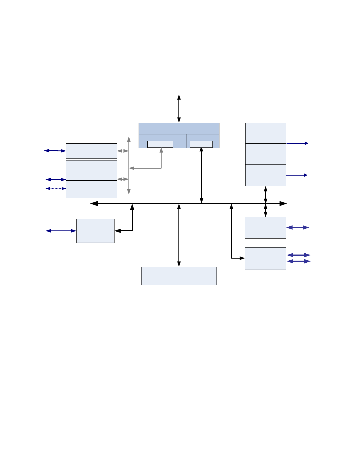
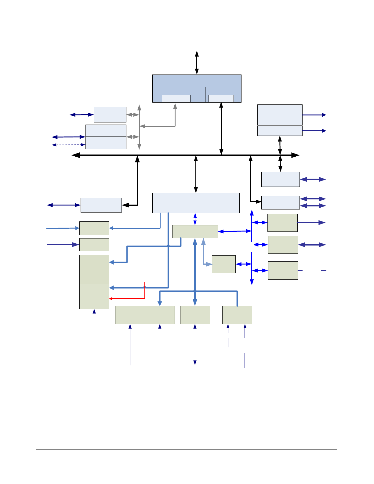
1.4 Block Diagrams
This section contains two block diagrams for the SB600. Figure 1 shows the SB600 internal PCI devices with
their assigned bus, device, and function numbers. Figure 2 shows the SB600 internal PCI devices and the
major function blocks.
ALINK-EXPRESS II
4 PORTS
10 PORTS
Debug port
SATA Controller 1
Bus 0 DEV 18 Function 0
USB:OHCI x5
Bus 0 DEV 19 Function 0:4
Device ID 4387h : 4388h :
4389h : 438Ah
Bus 0 DEV 19 Function 5
6 PCI SLOTS
Device ID 4380h
: 438Bh
USB:EHCI
Device ID 4386h
PCI Bridge
Bus 0 DEV 20
Function 4
Device ID 4384h
B-LINK A-LINK
PORT 1 PORT 0
B-LINK
ALINK
SMBUS /ACPI
Bus 0 DEV 20 Function 0
Device ID 4385h
AB
AC97 Audio
Bus 0 DEV 20
Function 5
Device ID 4382h
AC97 Modem
Bus 0 DEV 20
Function 6
Device ID 438Eh
HD Audio
Bus 0 DEV 20
Function 2
Device ID 4383h
IDE
Bus 0 DEV 20
Function 1
Device ID 438Ch
LPC
Bus 0 DEV 20
Function 3
Device ID 438Dh
AC97
1 CHANNEL
LPC bus
SPI bus
Figure 1 SB600 PCI Internal Devices
©2008 Advanced Micro Devices, Inc.
Block Diagrams
AMD SB600 Register Reference Manual Proprietary Page 11
Page 12
ALINK-EXPRESS II
AB
B-LINK A-LINK
PORT 1 PORT 0
10 PORTS
Debug port
6 PCI SLOTS
X1/X2
SERIRQ#
4 PORTS
SATA
Controller
USB:OHCI
USB:EHCI
PCI Bridge
RTC
SIRQ
APIC
PIC
B-LINK
PICD[0]
RTC_IRQ#,
PIDE_INTRQ,
SIDE_INTRQ,
USB_IRQ#,
AC97INTAB,
AC97INTBB
ALINK
SMBUS /ACPI
BUS Controler
BM
AC97 Modem
XBUS
AC97 Audio
HD Audio
IDE
LPC
ROM
GPIO
8250 TIMER
AC97
1
CHANNEL
LPC bus
SPI bus
SPEAKER
INTERRUPT
controller
INTR
IGNNE#,
FERRB#,
INT# F:A
SMI
ACPI / HW
Monitor
GEVENT[7:0],SLPBUTTON
TEMPDEAD, TEMPCAUT,
SHUTDOWN,DC_STOP#
SCIOUT, SLP#,
CPUSTP#, PCISTP#,
STPCLK#, SOFF#, SMI#,
SMIACT#
SMBUS
PM
PWRGOOD
CPURST,
INIT#,
RESET#
Figure 2 SB600 PCI Internal Devices and Major Function Blocks
©2008 Advanced Micro Devices, Inc.
Block Diagrams
AMD SB600 Register Reference Manual Proprietary Page 12
Page 13

2 Register Descriptions: PCI Devices
2.1 SATA Registers (Device 18, Function 0)
Note: Some SATA functions are controlled by, and associated with, certain PCI configuration registers in the
SMBus/ACPI device. For more information refer to section 2.3: SMBus Module and ACPI Block (Device 20,
Function 0). The diagram below lists these SATA functions and the associated registers.
SATA
SATA Enables
SATA power saving
SATA Interrupt Map register
SATA Smart Power Control
PCI_Reg:
5Ch 98h
2.1.1 PCI Configuration Space
The PCI Configuration Space registers define the operation of the SB600’s SATA controller on the PCI bus.
These registers are accessible only when the SATA controller detects a Configuration Read or Write
operation, with its IDSEL asserted, on the 32-bit PCI bus.
Register Name Offset Address
Vendor ID 00h
Device ID 02h
Command 04h
Status 06h
Revision ID/Class Code 08h
Cache Link Size 0Ch
Master Latency Timer 0Dh
Header Type 0Eh
BIST Mode Type 0Fh
Base Address 0 10h
Base Address 1 14h
Base Address 2 18h
Base Address 3 1Ch
Bus Master Interface Base Address 20h
AHCI Base Address 24h
Subsystem ID and Subsystem Vendor ID 2Ch
Capabilities Pointer 34h
Interrupt Line 3Ch
Interrupt Pin 3Dh
Min_gnt 3Eh
Max_latency 3Fh
Misc control 40h
Watch Dog Control And Status 44h
Watch Dog Counter 46h
MSI Control 50h
MSI Address 54h
MSI Upper Address 58h
MSI Data 5Ch
Power Management Capability ID 60h
Power Management Capability 62h
Power Management Control And Status 64h
AC/AFh
©2008 Advanced Micro Devices, Inc.
SATA Registers (Device 18, Function 0)
AMD SB600 Register Reference Manual Proprietary Page 13
Page 14

Register Name Offset Address
Serial ATA Capability Register 0 70h
Serial ATA Capability Register 1 74h
IDP Index 78h
IDP Data 7Ch
PHY Port0 Control 88h
PHY Port1 Control 8Ch
PHY Port2 Control 90h
PHY Port3 Control 94h
BIST pattern Count C0h
PCI Target Control TimeOut Counter C4h
Vendor ID - R - 16 bits - [PCI_Reg:00h]
Field Name Bits Default Description
Vendor ID 15:0 1002h This register holds a unique 16-bit value assigned to a vendor.
Combined with the device ID, it identifies any PCI device.
Device ID - R - 16 bits - [PCI_Reg:02h]
Field Name Bits Default Description
Device ID 15:0 4380h This register holds a unique 16-bit value assigned to a device.
Combined with the vendor ID, it identifies any PCI device.
4380h for the non-Raid5 controller
4381h for the Raid5 controller.
Bonding option default to the non-Raid 5 controller.
Command - RW - 16 bits - [PCI_Reg:04h]
Field Name Bits Default Description
I/O Access Enable 0 0b This bit controls access to the I/O space registers. When this
bit is 1, it enables the SATA controller to respond to PCI IO
space access.
Memory Access Enable 1 0b This bit controls access to the memory space registers. When
this bit is 1, it enables the SATA controller to respond to PCI
memory space access
Bus Master Enable 2 0b Bus master function enable.
1 = Enable
0 = Disable.
Special Cycle
Recognition Enable
Memory Write and
Invalidate Enable
VGA Palette Snoop
Enable
PERR- Detection Enable 6 0b If set to 1, the IDE host controller asserts PERR- when it is the
Wait Cycle Enable 7 0b Read Only.
SERR- Enable 8 0b If set to 1, and bit 6 is set, then the SATA controller asserts
Fast Back-to-Back
Enable
Interrupt Disable 10 0b Complies with the PCI 2.3 specification.
Reserved 15:11 Reserved.
3 0b Read Only. Hardwired to ‘0’
4 0b Read Only. Hardwired to ‘0’
5 0b Read Only. Hard-wired to ‘0’ indicating that the SATA host
controller does not need to snoop VGA palette cycles.
agent receiving data AND it detects a parity error. PERR- is
not asserted if this bit is 0.
Hard-wired to ‘0’ to indicate that the SATA controller does not
need to insert a wait state between the address and data on
the AD lines.
SERR- when it detects an address parity error. SERR- is not
asserted if this bit is 0.
9 0b Read Only. Hard-wired to ‘0’ to indicate that fast back to back
is only allowed to the same agent.
©2008 Advanced Micro Devices, Inc.
SATA Registers (Device 18, Function 0)
AMD SB600 Register Reference Manual Proprietary Page 14
Page 15

Status - RW - 16 bits - [PCI_Reg:06h]
Field Name Bits Default Description
Reserved 2:0 Reserved.
Interrupt Status 3 0b Interrupt status bit. Complies with the PCI 2.3 specification.
Capabilities List 4 1b Read Only. Hardwired to 1 to indicate that the Capabilities
Pointer is located at 34h.
66MHz Support 5 1b 66MHz capable. This feature is supported in the SATA
controller.
Reserved 6
Fast Back-to-Back
Capable
Data Parity Error 8 0b Data Parity reported. Set to 1 if the SATA controller detects
DEVSEL- Timing 10:9 01b Read only.
Signaled Target Abort 11 0b Signaled Target Abort. This bit is set to 1, when the SATA
Received Target Abort 12 0b Received Target Abort. This bit is set to 1 when the SATA
Received Master Abort
Status
SERR- Status 14 0b SERR- status. This bit is set to 1 when the SATA controller
Detected Parity Error 15 0b Detected Parity Error. This bit is set to 1 when the SATA
7 0b Read Only. Hard-wired to ‘0’ to indicate that it is fast back to
13 0b Received Master Abort Status. Set to 1 when the SATA
Reserved.
back incapable.
PERR- asserted while acting as the PCI master (whether
PERR- was driven by the SATA controller or not.). Write ‘1’ to
clear this bit.
These bits indicate DEVSEL- timing when performing a
positive decode. Since DEVSEL- is asserted to meet the
medium timing, these bits are encoded as 01b.
controller signals Target Abort. Write ‘1’ to clear this bit.
controller that generated the PCI cycle (SATA controller is the
PCI master) is aborted by a PCI target. Write ‘1’ to clear this
bit.
controller, acting as a PCI master, aborts a PCI bus memory
cycle. Write ‘1’ to clear this bit..
detects a PCI address parity error. Write ‘1’to clear this bit.
controller detects a parity error. Write ‘1’ to clear this bit.
Revision ID/Class Code- R - 32 bits - [PCI_Reg:08h]
Field Name Bits Default Description
Revision ID 7:0 00h These bits are hardwired to 00h to indicate the revision level of
the chip design.
Operating Mode
Selection
Sub-Class Code 23:16 01h Sub-Class Code. 01h to indicate an IDE Controller. See Note.
Class Code 31:24 01h Class Code. These 8 bits are read only and wired to 01h to
15:8 8Fh RW
Programmable I/F.
Bit [15] = Master IDE Device. Always 1.
Bits [14:12] = Reserved. Always read as 0’s.
Bit [11] = Programmable indicator for Secondary. Always 1 to
indicate that both modes are supported.
Bit [10] = Operating Mode for Secondary.
1 = Native PCI-mode.
0 = Compatibility Mode
Bit [9] = Programmable indicator for Primary. Always 1 to
indicate that both modes are supported.
Bit [8] = Operating Mode for Primary.
1 = Native PCI-mode.
0 = Compatibility
indicate a Mass-Storage Controller.
©2008 Advanced Micro Devices, Inc.
SATA Registers (Device 18, Function 0)
AMD SB600 Register Reference Manual Proprietary Page 15
Page 16

Revision ID/Class Code- R - 32 bits - [PCI_Reg:08h]
Field Name Bits Default Description
Note: This field is only writeable when PCI_Reg:40h[0] is set.
Sub-Class Code Program Interface Controller Type
01 8F IDE
06 01 AHCI
04 00 RAID
Cache Line Size - RW - 8 bits - [PCI_Reg:0Ch]
Field Name Bits Default Description
Reserved 3:0 Reserved.
Cache Line Size Register 7:4 0h If the value is 1, then the cache line size is 16 DW (64 byte).
Master Latency Timer - RW - 8 bits - [PCI_Reg:0 Dh]
Field Name Bits Default Description
Reserved 2:0 Reserved.
Master Latency Timer 7:3 00h Master Latency Timer. This number, in units of clocks,
represents the guaranteed time slice allowed to the IDE host
controller for burst transactions.
Header Type - R - 8 bits - [PCI_Reg:0Eh]
Field Name Bits Default Description
Header Type 7:0 00h Header Type. Since the IDE host controller is a single-function
device, this register contains a value of 00h.
BIST Mode Type - RW - 8 bits - [PCI_Reg:0Fh]
Field Name Bits Default Description
Completion Code 3:0 0h Read Only.
Indicates the completion code status of BIST. A non-zero
value indicates a failure.
Reserved 5:4 Reserved.
Start BIST 6 0b Since bit [7] is 0, program this bit take no effect.
BIST Capable 7 0b Read Only. Hard-wired to ‘0’ indicating that there is no HBA
related BIST function.
Base Address 0 - RW - 32 bits - [PCI_Reg:10h]
Field Name Bits Default Description
Resource Type Indicator 0 1b RTE (Resource Type Indicator). This bit is wired to 1 to
indicate that the base address field in this register maps to I/O
space.
Reserved 2:1 Reserved.
Primary IDE CS0 Base
Address
31:3 0000_
0000h
Base Address for Primary IDE Bus CS0. This register is used
for native mode only. Base Address 0 is not used in
compatibility mode.
Base Address 1 - RW - 32 bits - [PCI_Reg:14h]
Field Name Bits Default Description
Resource Type Indicator 0 1b RTE (Resource Type Indicator). This bit is wired to 1 to
indicate that the base address field in this register maps to I/O
space.
Reserved 1 Reserved.
Primary IDE CS1 Base
Address
31:2 0000_
0000h
Base Address for Primary IDE Bus CS1. This register is used
for native mode only. Base Address 1 is not used in
compatibility mode.
©2008 Advanced Micro Devices, Inc.
SATA Registers (Device 18, Function 0)
AMD SB600 Register Reference Manual Proprietary Page 16
Page 17

Base Address 2 - RW - 32 bits - [PCI_Reg:18h]
Field Name Bits Default Description
Resource Type Indicator 0 1b This bit is wired to 1 to indicate that the base address field in
this register maps to I/O space.
Reserved 2:1 Reserved.
Secondary IDE CS0
Base Address
31:3 0000_
0000h
Base Address for Secondary IDE Bus CS0. This register is
used for native mode only. Base Address 2 is not used in
compatibility mode.
Base Address 3 - RW - 32 bits - [PCI_Reg:1Ch]
Field Name Bits Default Description
Resource Type Indicator 0 1b This bit is wired to 1 to indicate that the base address field in
this register maps to I/O space.
Reserved 1 Reserved.
Secondary IDE CS1
Base Address
31:2 0000_
0000h
Base Address for Secondary IDE Bus CS1. This register is
used for native mode only. Base Address 3 is not used in
compatibility mode.
Bus Master Interface Base Address - RW - 32 bits - [PCI_ Reg:20h]
Field Name Bits Default Description
Resource Type Indicator 0 1b This bit is wired to 1 to indicate that the base address field in
this register maps to I/O space.
Reserved 3:1 Reserved.
Bus Master Interface
Register Base Address
31:4 0000_
000h
Base Address for the Bus Master interface registers, and
corresponds to AD[15:4].
AHCI Base Address - RW - 32 bits - [PCI_Reg:24h]
Field Name Bits Default Description
Resource Type Indicator 0 0b This bit is wired to 0 to indicate a request for register memory
space.
Reserved 9:1 Reserved.
AHCI Base Address 31:10 000000h Base address of register memory space. This represents a
memory space for support of 4 ports.
Subsystem ID and Subsystem Vendor ID - RW - 32 bits - [PCI_Reg:2Ch]
Field Name Bits Default Description
Subsystem Vendor ID 15:0 0000h Subsystem Vendor ID. This can only be written once by the
software.
Subsystem ID 31:16 0000h Subsystem ID. This can only be written once by the software.
Capabilities Pointer - R - 8 bits - [PCI_Reg:34h]
Field Name Bits Default Description
Capabilities Pointer 7:0 60h The first pointer of the Capability block
Interrupt Line - RW - 8 bits - [PCI_Reg:3Ch]
Field Name Bits Default Description
Interrupt Line 7:0 00h Identifies which input on the interrupt controller the function’s
PCI interrupt request pin (as specified in its Interrupt Pin
register) is routed to.
Interrupt Pin - R - 8 bits - [PCI_Reg:3Dh]
Field Name Bits Default Description
Interrupt Pin 7:0 01h Hard-wired to 01h.
©2008 Advanced Micro Devices, Inc.
SATA Registers (Device 18, Function 0)
AMD SB600 Register Reference Manual Proprietary Page 17
Page 18

Min_gnt - R - 8 bits - [PCI_Reg:3Eh]
Field Name Bits Default Description
Minimum Grant 7:0 00h This register specifies the desired settings for how long of a
burst the SATA controller needs. The value specifies a period
of time in units of ¼ microseconds.
Hard-wired to 0’s and always read as 0’s.
Max_latency - R - 8 bits - [PCI_Reg:3Fh]
Field Name Bits Default Description
Maximum Latency 7:0 00h This register specifies the Maximum Latency time required
before the SATA controller as a bus-master can start an
accesses
Hard-wired to 0’s and always read as 0’s.
Misc Control - RW - 32 bits - [PCI_Reg:40h]
Field Name Bits Default Description
Subclass code write
Enable
Disable Dynamic Sata
Memory Power Saving
Enable dynamic Sata
Core Power Saving
Reserved 3 Reserved.
Disable Speed up XP
Boot
Reserved 5 0b Reserved
Reserved 15:6 Reserved.
Disable port0 16 0b When set, port0 is disabled and port0 clock is shut down.
Disable port1 17 0b When set, port1 is disabled and port1 clock is shut down.
Disable port2 18 0b When set, port2 is disabled and port2 clock is shut down.
Disable port3 19 0b When set, port3 is disabled and port3 clock is shut down.
Reserved 31:20 Reserved.
0 0b Once set, Program Interface register (PCI_Reg:09h), subclass
code register (PCI_Reg:0Ah) and Multiple Message Capable
bits (PCI_Reg50h[19:17]) can be programmable.
1 0b When clear, dynamic power saving function for SATA internal
memory macros will be performed to reduce power
consumption.
2 0b When set, dynamic power saving function for SATA core clock
will be performed during partial/slumber mode to reduce power
consumption.
4 0b When clear, it fastens XP boot up in IDE mode. However, this
bit needs to be set, when enable SATA partial/slumber power
function is in IDE mode.
When set, the SATA partial/slumber power function can be
enabled in IDE mode, but the BIOS IO trap is needed to speed
up XP boot-up in IDE mode.
Please refer to BAR5 + offset 12C/1Ac/22C/2AC[11:8] for the
SATA partial/slumber modes that are allowed.
Watch Dog Control And Status - RW - 16 bits - [PCI_Reg:44h]
Field Name Bits Default Description
Watchdog Enable 0 0b Set this bit to enable the watchdog counter for all the PCI
down stream transaction.
Watchdog Timeout
Status
Reserved 15:2 Reserved.
1 0b Watchdog Counter Timeout Status bit. This bit indicates that
the watchdog counter has expired for PCI down stream
transaction and the transaction got aborted due to counter has
expired.
Software writes 1 to clear the status.
Watch Dog Counter - RW - 16 bits - [PCI_Reg:46h]
Field Name Bits Default Description
Watchdog Counter 7:0 80h Specifies the timeout retry count for PCI down stream retries.
Reserved 15:8 Reserved.
©2008 Advanced Micro Devices, Inc.
SATA Registers (Device 18, Function 0)
AMD SB600 Register Reference Manual Proprietary Page 18
Page 19

MSI Control - RW- 32 bits - [PCI_Reg:50h]
Field Name Bits Default Description
Capability ID 7:0 05h Read-Only.
Capability ID. It indicates that this is and MSI capability ID.
Capability Next Pointer 15:8 70h Read-Only.
Next Pointer (hard wired to 70h, points to Index Data pair
capability
Message Signaled
Interrupt Enable
Multiple Message
Capable
Multiple Message Enable 22:20 000b Multiple Message Enable.
MSI 64-bit Address 23 1b Read-Only
Reserved 31:24 Reserved.
16 0b MSI Enable.
19:17 010b Multiple Message Capable.
Support 64-bit address.
MSI Address - RW- 32 bits - [PCI_Reg:54h]
Field Name Bits Default Description
Reserved 1:0 Reserved.
MSI Address 31:2 0000_0000h Lower 32 bits of the system specified message address
always DW aligned.
MSI Upper Address - RW- 32 bits - [PCI_Reg:58h]
Field Name Bits Default Description
MSI Upper Address 31:0 0000_0000h Upper 32 bits of the system specified message address.
This register is optional and only implemented if
MC.C64=1.
MSI Data - RW- 16 bits - [PCI_Reg:5Ch]
Field Name Bits Default Description
MSI Data 15:0 0000h MSI Data
Power Management Capability ID - R- 16 bits - [PCI_Reg:60h]
Field Name Bits Default Description
Capability ID 7:0 01h Capability ID. Indicates this is power management capability
ID.
Capability Next Pointer 15:8 50h Next Pointer.
Power Management Capability - R- 16 bits - [PCI_Reg:62h]
Field Name Bits Default Description
Version 2:0 010b Indicates support for Revision 1.1 of the PCI Power
Management Specification.
PME Clock 3 0b Indicates that PCI clock is not required to generate PME#.
Reserved 4 Reserved
Device Specific
Initialization
Aux_Current 8:6 000b Reports the maximum Suspend well current required when
D1_Support 9 0b The D1 state is not supported.
D2_Support 10 0b The D2 state is not supported.
PME_Support 15:11 00h Read-Only.
5 1b Indicates whether device-specific initialization is required.
in the D3
state. Hard wired to 000b.
COLD
©2008 Advanced Micro Devices, Inc.
SATA Registers (Device 18, Function 0)
AMD SB600 Register Reference Manual Proprietary Page 19
Page 20

PCI Power Management Control And Status - RW- 16 bits - [PCI_Reg:64h]
Field Name Bits Default Description
Power State 1:0 00b
Reserved 7:2 Reserved
PME Enable 8 0b Read-only. Hard-wired to ‘0’ indicates PME disable
Reserved 14:9 Reserved.
PME Status 15 0b Read-only. Hard-wired to ‘0’ as PME disable
This field is used both to determine the current power state
of the HBA and to set a new power state. The values are:
00 – D0 state
11 – D3
The D1 and D2 states are not supported. When in the
state, the configuration space is available, but the
D3
HOT
register memory spaces are not. Additionally, interrupts
are blocked.
HOT
state
Serial ATA Capability Register 0 - R- 32 bits - [PCI_Reg:70h]
Field Name Bits Default Description
Capability ID 7:0 12h Capability ID. Indicates this is a Serial ATA Capability ID.
Capability Next Pointer 15:8 00h Next Pointer, end of the list.
Minor Revision 19:16 0h Minor revision number of the SATA Capability Pointer
implemented.
Major Revision 23:20 1h Major revision number of the SATA Capability Pointer
implemented.
Reserved 31:24 Reserved
Serial ATA Capability Register 1 - R- 32 bits - [PCI_Reg:74h]
Field Name Bits Default Description
BAR Location 3:0 1111b Value 1111b indicates that the Index-Data Pair is implemented
in Dwords directly following SATACR1 in the PCI configuration
space.
BAR Offset 23:4 00000h Indicates the offset into the BAR where the Index-Data Pair
are located in Dword granularity. Since the BAR location is
setting at 1111b, this field is not used anymore.
Reserved 31:24 Reserved
IDP Index Register - RW- 32 bits - [PCI_Reg:78h]
Field Name Bits Default Description
Reserved 1:0 Reserved
IDP Index 9:2 00h This register selects the Dword offset of the memory mapped
AHCI register to be accessed. The IDP Index should be sized
such that it can access the entire ABAR register space for the
particular implementation. See Note.
Reserved 31:10 Reserved
Note: ABAR is AHCI memory map registers located at AHCI base address (BAR5) space.
IDP Data Register - RW- 32 bits - [PCI_Reg:7Ch ]
Field Name Bits Default Description
IDP Data 31:0 This register is a “window” through which data is read or
written to the memory mapped register pointed to by the IDP
Index register. Note that a physical register is not actually
implemented as the data is actually stored in the memory
mapped registers.
Since this is not a physical register, the “default” value is the
same as the default value of the register pointed to by IDP
Index.
All register accesses to IDP Data are Dword granularity
©2008 Advanced Micro Devices, Inc.
SATA Registers (Device 18, Function 0)
AMD SB600 Register Reference Manual Proprietary Page 20
Page 21

PHY Port0 Control - RW- 32 bits - [PCI_Reg:88h]
Field Name Bits Default Description
Port0 PHY 23:0 B40014h PHY port0 fine-tune register.
TX main driver swing 4:0 10100b Port0 Tx driving swing[4:0] is valid for SATA 1.5G. It sets the
TX main driver swing. The user can program the optimum
value for each SATA port.
Bit 4 Bit 3 Bit 2 Bit 1 Bit0 Nominal Output
1 0 0 0 0 400mv
1 0 0 1 0 450mv
1 0 1 0 0 500mv
1 0 1 1 0 550mv
1 1 0 0 0 600mv
1 1 0 1 0 650mv
1 1 1 0 0 700mv
1 1 1 1 0 750mv
Note: This applies to all the ASIC Revisions A11 and above.
TX pre-emphasis driver
swing
TX pre-emphasis enable 13 0b Turns on TX pre-emphasis output
Reserved 31:24 Reserved.
7:5 000b Port0 Tx driving swing[7:5] is valid for both SATA 3G and
1.5G. It sets the TX pre-emphasis driver strength. The user
can program the optimum pre-emphasis value for each SATA
port if TX pre-emphasis enable bit is turned on.
Bit 7 Bit 6 Bit 5 pre-emphasis amount
0 0 0 0mv
0 0 1 25mv
0 1 0 50mv
0 1 1 75mv
1 0 0 100mv
1 0 1 125mv
1 1 0 150mv
1 1 1 175mv
Note: This applies to all the ASIC Revisions A11 and above.
1: Enable pre-emphasis
0: Disable pre-emphasis
PHY Port1 Control - RW- 32 bits - [PCI_Reg:8Ch]
Field Name Bits Default Description
Port1 PHY 23:0 B40014h PHY port1 fine-tune register.
TX main swing 4:0 10100b Port1 Tx driving swing[4:0] is valid at SATA 1.5G. It sets the
TX main driver swing. The user can program the optimum
value for each SATA port.
Bit 4 Bit 3 Bit 2 Bit 1 Bit 0 Nominal Output
1 0 0 0 0 400mv
1 0 0 1 0 450mv
1 0 1 0 0 500mv
1 0 1 1 0 550mv
1 1 0 0 0 600mv
1 1 0 1 0 650mv
1 1 1 0 0 700mv
1 1 1 1 0 750mv
Note: This applies to all the ASIC Revisions A11 and above.
©2008 Advanced Micro Devices, Inc.
SATA Registers (Device 18, Function 0)
AMD SB600 Register Reference Manual Proprietary Page 21
Page 22

PHY Port1 Control - RW- 32 bits - [PCI_Reg:8Ch]
Field Name Bits Default Description
TX pre-emphasis driver
swing
TX pre-emphasis enable 13 0b Turns on port1 TX pre-emphasis output.
7:5 000b Port1 Tx driving swing[7:5] is valid for both SATA 3G and
1.5G. It sets the TX pre-emphasis driver strength. The user
can program the optimum pre-emphasis value for each SATA
port if TX pre-emphasis enable bit turned on.
Bit 7 Bit 6 Bit 5 pre-emphasis amount
0 0 0 0mv
0 0 1 25mv
0 1 0 50mv
0 1 1 75mv
1 0 0 100mv
1 0 1 125mv
1 1 0 150mv
1 1 1 175mv
Note: This applies to all the ASIC Revisions A11 and above.
1: Enable pre-emphasis
0: Disable pre-emphasis
PHY Port2 Control - RW- 32 bits - [PCI_Reg:90h]
Field Name Bits Default Description
Port2 PHY 23:0 B40014h PHY port2 fine-tune register.
TX main swing 4:0 10100b Port2 Tx driving swing[4:0] is valid at SATA 1.5G.
Bit 4 Bit 3 Bit 2 Bit 1 Bit 0 Nominal Output
1 0 0 0 0 400mv
1 0 0 1 0 450mv
1 0 1 0 0 500mv
1 0 1 1 0 550mv
1 1 0 0 0 600mv
1 1 0 1 0 650mv
1 1 1 0 0 700mv
1 1 1 1 0 750mv
Note: This applies to all the ASIC Revisions A11 and above.
TX pre-emphasis driver
swing
TX pre-emphasis enable 13 0b Turns on port2 TX pre-emphasis output
7:5 000b Port2 Tx driving swing[7:5] is valid for both SATA 3G and
1.5G. It sets the TX pre-emphasis driver strength. The user
can program the optimum pre-emphasis value for each SATA
port if TX pre-emphasis enable bit turned on.
Bit 7 Bit 6 Bit 5 pre-emphasis amount
0 0 0 0mv
0 0 1 25mv
0 1 0 50mv
0 1 1 75mv
1 0 0 100mv
1 0 1 125mv
1 1 0 150mv
1 1 1 175mv
Note: This applies to all the ASIC Revisions A11 and above.
1: Enable pre-emphasis
0: Disable pre-emphasis
©2008 Advanced Micro Devices, Inc.
SATA Registers (Device 18, Function 0)
AMD SB600 Register Reference Manual Proprietary Page 22
Page 23

PHY Port3 Control - RW- 32 bits - [PCI_Reg:94h]
Field Name Bits Default Description
Port3 PHY 23:0 B40014h PHY port3 fine-tune register.
TX main swing 4:0 10100b Port3 Tx driving swing[4:0] is valid at SATA 1.5G.
Bit 4 Bit 3 Bit 2 Bit 1 Bit 0 Nominal Output
1 0 0 0 0 400mv
1 0 0 1 0 450mv
1 0 1 0 0 500mv
1 0 1 1 0 550mv
1 1 0 0 0 600mv
1 1 0 1 0 650mv
1 1 1 0 0 700mv
1 1 1 1 0 750mv
Note: This applies to all the ASIC Revisions A11 and above.
TX pre-emphasis driver
swing
TX pre-emphasis enable 13 0b Turns on port3 TX pre-emphasis output
7:5 000b Port3 Tx driving swing[7:5] is valid for both SATA 3G and
1.5G. It sets the TX pre-emphasis driver strength. The user
can program the optimum pre-emphasis value for each SATA
port if TX pre-emphasis enable bit turned on.
Bit 7 Bit 6 Bit 5 pre-emphasis amount
0 0 0 0mv
0 0 1 25mv
0 1 0 50mv
0 1 1 75mv
1 0 0 100mv
1 0 1 125mv
1 1 0 150mv
1 1 1 175mv
Note: This applies to all the ASIC Revisions A11 and above.
1: Enable pre-emphasis
0: Disable pre-emphasis
BIST Pattern Count - RW - 32 bits - [PCI_Reg:C0h]
Field Name Bits Default Description
BIST Pattern Count 31:0 0000_20
00h
This count specifies how many Octal WORD pattern need to
be checked before BIST Done bit be set. This count value is
used fro all the 4 ports. 400h default value would be used for
tester, which means 32K DWORD pattern would be compared
for BIST test. Value of “0000_0000”h means the maximum
patterns (16,000, 000, 000) checked.
PCI Target Control TimeOut Counter - RW – 8 bits - [PCI_Reg:C4h]
Field Name Bits Default Description
PCI Target Control
TimeOut Count
7:0 80h This register is used for programming the PCI Target Control
TimeOut Count used to clear any stale target commands to
the hosts controller. Granularity is 15.5us (Count * 15.5 us)
The counter will be disabled if the count is programmed to 0x0.
©2008 Advanced Micro Devices, Inc.
SATA Registers (Device 18, Function 0)
AMD SB600 Register Reference Manual Proprietary Page 23
Page 24
2.1.2 BAR0/BAR2/BAR1/BAR3 Registers (SATA I/O Register for IDE mode)
BAR0/BAR2 uses 8 bytes of I/O space. BAR0 is used for Primary channel and BAR2 is used for Secondary
channel during IDE native mode. BAR1/BAR3 uses 2 bytes of I/O space. BAR1 is used for Primary channel
and BAR3 is used for Secondary channel during IDE native mode.
Address (hex) Name and Function
Compatibility Mode Native Mode (Offset) Read Function Write Function
IDE Command Block Registers
Primary Secondary BAR0/BAR2
1F0 170 (Primary or Secondary)
Base Address 0 + 0
1F1 171 (Primary or Secondary)
Base Address 0 + 1
1F2 172 (Primary or Secondary)
Base Address 0 + 2
1F3 173 (Primary or Secondary)
Base Address + 3
1F4 174 (Primary or Secondary)
Base Address + 4
1F5 175 (Primary or Secondary)
Base Address + 5
1F6 176 (Primary or Secondary)
Base Address + 6
1F7 177 (Primary or Secondary)
Base Address + 7
IDE Control Block Registers
Primary Secondary BAR1/BAR3
3F6 376 (Primary or Secondary)
Base Address + 2
Data (16 bit) Data (16 bit)
Error register Features register
Sector Count Sector Count
Sector Number Sector Number
Cylinder Low Cylinder Low
Cylinder High Cylinder High
Drive/Head Drive/Head
Status Command
Alternate Status Device Control
2.1.3 BAR4 Registers (SATA I/O Register for IDE mode)
BAR4 uses 16 bytes of I/O space. The Bus-master interface base address register (BAR4) defines the base
address of the IO spare.
Register Name Offset Address
[Primary/Secondary]
Bus-master IDE Command 00h/08h
Bus-master IDE Status 02h/0Ah
Descriptor Table Pointer 04h/0Ch
Bus-master IDE Command - RW- 8 bits - [IO_Reg: BAR4 + 00/08h]
Field Name Bits Default Description
Bus Master IDE
Start/Stop
Reserved 2:1 Reserved.
Bus Master Read/Write 3 0b Bus Master IDE r/w (direction) control
Reserved 7:4 Reserved.
0 0b Bus Master IDE Start (1)/Stop (0).
This bit will not be reset by interrupt from IDE device. This must
be reset by soft ware (device driver).
0 = Memory -> IDE
1 = IDE -> Memory
This bit should not change during Bus Master transfer cycle, even
if terminated by Bus Master IDE stop.
©2008 Advanced Micro Devices, Inc.
SATA Registers (Device 18, Function 0)
AMD SB600 Register Reference Manual Proprietary Page 24
Page 25

Bus-master IDE Status - RW- 8 bits - [IO_Reg: BAR4 + 02/0Ah]
Field Name Bits Default Description
Bus Master Active 0 0b Bus Master IDE active. This bit is set to 1 when bit 0 in the Bus
Master IDE command address register is set to 1. The IDE host
controller sets this bit to 0 when the last transfer for a region is
performed. This bit is also set to 0 when bit 0 of the Bus Master
IDE command register is set to 0.
Bus Master DMA Error 1 0b IDE DMA error. This bit is set when the IDE host controller
encounters a target abort, master abort, or Parity error while
transferring data on the PCI bus. Write ‘1’ clears this bit
IDE Interrupt 2 0b IDE Interrupt. Indicates when an IDE device has asserted its
interrupt line. IRQ14 is used for the Primary channel and IRQ15 is
used for the secondary channel. If the interrupt status bit is set to
0, by writing a 1 to this bit while the interrupt line is still at the
active level, this bit remains 0 until another assertion edge is
detected on the interrupt line.
Reserved 4:3 Reserved.
Master Device DMA
Capable
Slave Device DMA
Capable
Simplex Only 7 0b Read Only
5 0b Device 0 (Master) DMA capable.
6 0b Device 1 (Slave) DMA capable.
Simplex only. This bit is hard-wired as 0.
Descriptor Table Pointer - RW- 32 bits - [IO_Reg: BAR4 + 04/0Ch]
Field Name Bits Default Description
Reserved 1:0 0h Reserved. Always read as 0’s.
Descriptor Table Base
Address
31:2 0000_0000h Base Address of Descriptor Table. These bits correspond to
Address [31-02].
2.1.4 BAR5 Registers
These are the AHCI memory map registers. The base address is defined through the ABAR (BAR5) register.
Register Name Offset Address
Generic Host Control 00h-23h
Reserved
Vendor Specific registers A0h-FFh
Port 0 port control registers 100h-17Fh
Port 1 port control registers 180h-1FFh
Port 2 port control registers 200h-27Fh
Port 3 port control registers 280h-2FFh
24h-9Fh
2.1.4.1 Generic Host Control
The following registers apply to the entire HBA.
Register Name Offset Address
Host Capabilities(CAP) 00h-03h
Global Host Control(GHC) 04h-07h
Interrupt Status(IS) 08h-0Bh
Ports Implemented(PI) 0Ch-0Fh
Version(VS) 10h-13h
Command Completion Coalescing Control(CCC_CTL) 14h-17h
Command Completion Coalescing Ports(CCC_PORTS) 18h-1Bh
Enclosure Management Location(EM_LOC) 1Ch-1Fh
Enclosure Management Control(EM_CTL) 20h-23h
©2008 Advanced Micro Devices, Inc.
SATA Registers (Device 18, Function 0)
AMD SB600 Register Reference Manual Proprietary Page 25
Page 26

HBA Capabilities – R - 32bits [Mem_reg: ABAR + 00h]
Field Name Bits Default Description
Number of Ports(NP) 4:0 00011b 0’s based value indicating the maximum number of ports
supported by the HBA silicon. A maximum of 32 ports can be
supported. A value of ‘0h’, indicating one port, is the
minimum requirement. Note that the number of ports
indicated in this field may be more than the number of ports
indicated in the GHC.PI register.
Supports External SATA
(SXS)
Enclosure Management
Supported (EMS)
Command Completion
Coalescing Supported
(CCCS)
Number of Command
Slots (NCS)
Partial State Capable
(PSC)
Slumber State Capable
(SSC)
PIO Multiple DRQ Block
(PMD)
FIS-based Switching
Supported (FBSS)
5 0b When set to ‘1’, indicates that the HBA has one or more
Serial ATA ports that has a signal only connector that is
externally accessible. If this bit is set to ‘1’, software may
refer to the PxCMD.ESP bit to determine whether a specific
port has its signal connector externally accessible as a signal
only connector (i.e. power is not part of that connector).
When the bit is cleared to ‘0’, indicates that the HBA has no
Serial ATA ports that have a signal only connector externally
accessible.
6 0b When set to ‘1’, indicates that the HBA supports enclosure
management. When enclosure management is supported,
the HBA has implemented the EM_LOC and EM_CTL global
HBA registers. When cleared to ‘0’, indicates that the HBA
does not support enclosure management and the EM_LOC
and EM_CTL global HBA registers are not implemented.
7 1b When set to ‘1’, indicates that the HBA supports command
completion coalescing. When command completion
coalescing is supported, the HBA has implemented the
CCC_CTL and the CCC_PORTS global HBA registers.
When cleared to ‘0’, indicates that the HBA does not support
command completion coalescing and the CCC_CTL and
CCC_PORTS global HBA registers are not implemented.
12:8 11111b 0’s based value indicating the number of command slots per
port supported by this HBA. A minimum of 1 and maximum
of 32 slots per port can be supported. The same number of
command slots is available on each implemented port.
13 1b Indicates whether the HBA can support transitions to the
Partial state. When cleared to ‘0’, software must not allow
the HBA to initiate transitions to the Partial state via
aggressive link power management nor the PxCMD.ICC field
in each port, and the PxSCTL.IPM field in each port must be
programmed to disallow device initiated Partial requests.
When set to ‘1’, HBA and device initiated Partial requests can
be supported.
14 1b Indicates whether the HBA can support transitions to the
Slumber state. When cleared to ‘0’, software must not allow
the HBA to initiate transitions to the Slumber state via
aggressive link power management nor the PxCMD.ICC field
in each port, and the PxSCTL.IPM field in each port must be
programmed to disallow device initiated Slumber requests.
When set to ‘1’, HBA and device initiated Slumber requests
can be supported.
15 1b If set to ‘1’, the HBA supports multiple DRQ block data
transfers for the PIO command protocol. If cleared to ‘0’ the
HBA only supports single DRQ block data transfers for the
PIO command protocol.
16 0b When set to ‘1’, indicates that the HBA supports Port
Multiplier FIS-based switching. When cleared to ‘0’, indicates
that the HBA does not support FIS-based switching. AHCI
1.0 and 1.1 HBAs shall have this bit cleared to ‘0’.
©2008 Advanced Micro Devices, Inc.
SATA Registers (Device 18, Function 0)
AMD SB600 Register Reference Manual Proprietary Page 26
Page 27

HBA Capabilities – R - 32bits [Mem_reg: ABAR + 00h]
Field Name Bits Default Description
Supports Port Multiplier
(SPM)
Supports AHCI mode
only (SAM)
Supports Non-Zero DMA
Offsets (SNZO)
Interface Speed Support
(ISS)
Supports Command List
Override (SCLO)
Supports Activity LED
(SAL)
Supports Aggressive
Link Power Management
(SALP)
Supports Staggered
Spin-up (SSS)
Supports Mechanical
Presence Switch (SMPS)
Supports SNotification
Register (SSNTF)
17 1b Indicates whether the HBA can support a Port Multiplier.
When set, a Port Multiplier using command-based switching
is supported. When cleared to ‘0’, a Port Multiplier is not
supported, and a Port Multiplier may not be attached to this
HBA.
18 0b The SATA controller may optionally support AHCI access
mechanisms only. A value of '0' indicates that in addition to
the native AHCI mechanism (via ABAR), the SATA controller
implements a legacy, task-file based register interface such
as SFF-8038i. A value of '1' indicates that the SATA
controller does not implement a legacy, task-file based
register interface.
19 0b When set to ‘1’, indicates that the HBA can support non-zero
DMA offsets for DMA Setup FISes. This bit is reserved for
future AHCI enhancements. AHCI 1.0 and 1.1 HBAs shall
have this bit cleared to ‘0’.
23:20 2h
24 1b When set to ‘1’, the HBA supports the PxCMD.CLO bit and its
25 1b When set to ‘1’, the HBA supports a single activity indication
26 1b When set to ‘1’, the HBA can support auto-generating link
27 0b When set to ‘1’, the HBA supports staggered spin-up on its
28 1b When set to ‘1’, the HBA supports mechanical presence
29 1b
Indicates the maximum speed the HBA can support on its
ports. These encodings match the system software
programmable PxSCTL.DET.SPD field. Values are:
Bits Definition
0000 Reserved
0001 Gen 1 (1.5 Gbps)
0010
0011 - 1111 Reserved
associated function. When cleared to ‘0’, the HBA is not
capable of clearing the BSY and DRQ bits in the Status
register in order to issue a software reset if these bits are still
set from a previous operation.
output pin. This pin can be connected to an LED on the
platform to indicate device activity on any drive. When
cleared to ‘0’, this function is not supported.
requests to the Partial or Slumber states when there are no
commands to process. When cleared to ‘0’, this function is
not supported and software shall treat the PxCMD.ALPE and
PxCMD.ASP bits as reserved.
ports, for use in balancing power spikes. When cleared to ‘0’,
this function is not supported. This value is loaded by the
BIOS prior to OS initialization.
switches on its ports for use in hot plug operations. When
cleared to ‘0’, this function is not supported. This value is
loaded by the BIOS prior to OS initialization.
When set to ‘1’, the
HBA supports the PxSNTF
(SNotification) register and its associated functionality.
When cleared to ‘0’, the HBA does not support the
PxSNTF (SNotification) register and its associated
functionality.
Gen 1 (1.5 Gbps) and Gen 2 (3
Gbps)
©2008 Advanced Micro Devices, Inc.
SATA Registers (Device 18, Function 0)
AMD SB600 Register Reference Manual Proprietary Page 27
Page 28

HBA Capabilities – R - 32bits [Mem_reg: ABAR + 00h]
Field Name Bits Default Description
Supports Native
Command Queuing
(SNCQ)
Supports 64-bit
Addressing (S64A)
30 1b Indicates whether the HBA supports Serial ATA native
command queuing. If set to ‘1’, an HBA shall handle DMA
Setup FISes natively, and shall handle the auto-activate
optimization through that FIS. If cleared to ‘0’, native
command queuing is not supported and software should not
issue any native command queuing commands.
31 1b Indicates whether the HBA can access 64-bit data structures.
When set to ‘1’, the HBA shall make the 32-bit upper bits of
the port DMA Descriptor, the PRD Base, and each PRD entry
read/write. When cleared to ‘0’, these are read-only and
treated as ‘0’ by the HBA.
Global HBA Control – RW - 32bits [Mem_reg: ABAR + 04h]
Field Name Bits Default Description
HBA Reset (HR) 0 0b
Interrupt Enable (IE) 1 0b This global bit enables interrupts from the HBA. When
MSI Revert to Single
Message (MRSM)
Reserved 30:3 Reserved.
2 0b
When set by SW, this bit causes an internal reset of the HBA.
All state machines that relate to data transfers and queuing
shall return to an idle condition, and all ports shall be reinitialized via COMRESET (if staggered spin-up is not
supported). If staggered spin-up is supported, then it is the
responsibility of software to spin-up each port after the reset
has completed.
When the HBA has performed the reset action, it shall reset
this bit to ‘0’. A software write of ‘0’ shall have no effect. For
a description on which bits are reset when this bit is set.
cleared (reset default), all interrupt sources from all ports are
disabled. When set, interrupts are enabled.
Read Only
When set to ‘1’ by hardware, indicates that the HBA
requested more than one MSI vector but has reverted to
using the first vector only. When this bit is cleared to ‘0’, the
HBA has not reverted to single MSI mode (i.e. hardware is
already in single MSI mode, software has allocated the
number of messages requested, or hardware is sharing
interrupt vectors if MC.MME < MC.MMC).
The HBA may revert to single MSI mode when the number of
vectors allocated by the host is less than the number
requested. This bit shall only be set to ‘1’ when the following
conditions hold:
• MC.MSIE = ‘1’ (MSI is enabled)
• MC.MMC > 0 (multiple messages requested)
• MC.MME > 0 (more than one message allocated)
• MC.MME != MC.MMC (messages allocated not
equal to number requested)
When this bit is set to ‘1’, single MSI mode operation is in use
and software is responsible for clearing bits in the IS register
to clear interrupts.
This bit shall be cleared to ‘0’ by hardware when any of the
four conditions stated is false. This bit is also cleared to ‘0’
when MC.MSIE = ‘1’ and MC.MME = 0h. In this case, the
hardware has been programmed to use single MSI mode,
and is not “reverting” to that mode.
©2008 Advanced Micro Devices, Inc.
SATA Registers (Device 18, Function 0)
AMD SB600 Register Reference Manual Proprietary Page 28
Page 29

Global HBA Control – RW - 32bits [Mem_reg: ABAR + 04h]
Field Name Bits Default Description
AHCI Enable (AE) 31 0b
Interrupt Status - RW -32 bits [Mem_reg: ABAR + 08h]
Field Name Bits Default Description
Interrupt Pending Status
(IPS)
Write 1 to clear these status bits.
31:0 0000_
0000h
When set, indicates that communication to the HBA shall be
via AHCI mechanisms. This can be used by an HBA that
supports both legacy mechanisms (such as SFF-8038i) and
AHCI to know when the HBA is running under an AHCI
driver.
When set, software shall only communicate with the HBA
using AHCI. When cleared, software shall only communicate
with the HBA using legacy mechanisms. When cleared
FISes are not posted to memory and no commands are sent
via AHCI mechanisms.
Software shall set this bit to ‘1’ before accessing other AHCI
registers.
If set, indicates that the corresponding port has an interrupt
pending. Software can use this information to determine
which ports require service after an interrupt.
The IPS[x] bit is only defined for ports that are implemented
or for the command completion coalescing interrupt defined
by CCC_CTL.INT. All other bits are reserved.
Ports Implemented Register - R -32 bits [Mem_reg: ABAR + 0Ch]
Field Name Bits Default Description
Port Implemented (PI) 31:0 0000000Fh This register is bit significant. If a bit is set to ‘1’, the
corresponding port is available for software to use. If a bit is
cleared to ‘0’, the port is not available for software to use.
The maximum number of bits set to ‘1’ shall not exceed
CAP.NP + 1, although the number of bits set in this register
may be fewer than CAP.NP + 1. At least one bit shall be set
to ‘1’.
AHCI Version- R – 32 bits [Mem_reg: ABAR + 10h]
Field Name Bits Default Description
Minor Version Number
(MNR)
Major Version Number
(MJR)
Version: V1.10
15:0 0100h Indicates the minor version is “10”.
31:16 0001h Indicates the major version is “1”
Command Completion Coalescing Control(CCC_CTL) - RW – 32 bits [Mem_reg: ABAR + 14h]
Field Name Bits Default Description
CCC_CTL Enable 0 0b When cleared to ‘0’, the command completion coalescing
feature is disabled and no CCC interrupts are generated.
When set to ‘1’, the command completion coalescing feature
is enabled and CCC interrupts may be generated based on
timeout or command completion conditions. Software shall
only change the contents of the TV and CC fields when EN is
cleared to ‘0’. On transition of this bit from ‘0’ to ‘1’, any
updated values for the TV and CC fields shall take effect.
Reserved 2:1 Reserved
©2008 Advanced Micro Devices, Inc.
SATA Registers (Device 18, Function 0)
AMD SB600 Register Reference Manual Proprietary Page 29
Page 30

Command Completion Coalescing Control(CCC_CTL) - RW – 32 bits [Mem_reg: ABAR + 14h]
Field Name Bits Default Description
CCC Interrupt (INT) 7:3 1Fh Read Only
Specifies the interrupt used by the CCC feature. This
interrupt must be marked as unused in the Ports
Implemented (PI) register by the corresponding bit being set
to ‘0’. Thus, the CCC interrupt corresponds to the interrupt
for an unimplemented port on the controller. When a CCC
interrupt occurs, the IS.IPS[INT] bit shall be asserted to ‘1’.
This field also specifies the interrupt vector used for MSI.
Command Completions
(CC)
Timeout Value (TV) 31:16 0001h The timeout value is specified in 1 millisecond intervals. The
15:8 01h Specifies the number of command completions that are
necessary to cause a CCC interrupt. The HBA has an
internal command completion counter, hCccComplete.
hCccComplete is incremented by one each time a selected
port has a command completion. When hCccComplete is
equal to the command completions value, a CCC interrupt is
signaled. The internal command completion counter is reset
to ‘0’ on the assertion of each CCC interrupt. A value of ‘0’
for this field shall disable CCC interrupts being generated
based on the number of commands completed, i.e. CCC
interrupts are only generated based on the timer in this case.
timer accuracy shall be within 5%. hCccTimer is loaded with
this timeout value. The hCccTimer is only decremented when
commands are outstanding on selected ports. The HBA will
signal a CCC interrupt when hCccTimer has decremented to
‘0’. The hCccTimer is reset to the timeout value on the
assertion of each CCC interrupt. A timeout value of ‘0’ is
reserved.
Command Completion Coalescing Ports - RW – 32 bits [Mem_reg: ABAR + 18h]
Field Name Bits Default Description
Ports (PRT) 31:0 00000000h This register is bit significant. Each bit corresponds to a
particular port, where bit 0 corresponds to port 0. If a bit is
set to ‘1’, the corresponding port is part of the command
completion coalescing feature. If a bit is cleared to ‘0’, the
port is not part of the command completion coalescing
feature. Bits set to ‘1’ in this register must also have the
corresponding bit set to ‘1’ in the Ports Implemented register.
An updated value for this field shall take effect within one
timer increment (1 millisecond).
©2008 Advanced Micro Devices, Inc.
SATA Registers (Device 18, Function 0)
AMD SB600 Register Reference Manual Proprietary Page 30
Page 31

2.1.4.2 Port Registers (One Set Per Port)
The algorithm for the software to determine the offset is as follows:
• Port offset = 100h + (PI Asserted Bit Position * 80h)
Register Name Offset Address
Port-N Command List Base Address(PNCLB) 00h-03h + Port offset
Port-N Command List Base Address Upper 32-
Bits(PNCLBU)
Port-N FIS Base Address(PNFB) 08h-0Bh + Port offset
Port-N FIS Base Address Upper 32-Bits(PNFBU) 0Ch-0Fh + Port offset
Port-N Interrupt Status(PNIS) 10h-13h + Port offset
Port-N Interrupt Enable(PNIE) 14h-17h + Port offset
Port-N Command and Status(PNCMD) 18h-1Bh + Port offset
Reserved 1Ch-1Fh + Port offset
Port-N Task File Data(PNTFD) 20h-23h + Port offset
Port-N Signature(PNSIG) 24h-27h + Port offset
Port-N Serial ATA Status (PNSSTS) 28h-2Bh + Port offset
Port-N Serial ATA Control (PNSCTL) 2Ch-2Fh + Port offset
Port-N Serial ATA Error (PNSERR) 30h-33h + Port offset
Port-N Serial ATA Active (PNSACT) 34h-37h + Port offset
Port-N Command Issue(PNCI) 38h-3Bh + Port offset
Port-N SNotification (PNSNTF) 3Ch-3Fh + Port offset
Reserved for FIS-based Switching Definition 40h-43h + Port offset
Reserved 44h-6Fh + Port offset
Port-N Vendor Specific(PNVS) 70h-7Fh + Port offset
*N is the port number, 0 ~ 3
04h-07h + Port offset
Port-N Command List Base Address -RW -32 bits [Mem_reg: ABAR + port offset + 00h ]
Field Name Bits Default Description
Reserved 9:0 Reserved.
Command List Base
Address (CLB)
31:10 000000h Indicates the 32-bit base physical address for the command
list for this port. This base is used when fetching commands
to execute. The structure pointed to by this address range is
1K-bytes in length. This address must be 1K-byte aligned as
indicated by bits 09:00 being read only.
Port-N Command List Base Upper Address -RW - 32 bits [Mem_reg: ABAR + port offset + 04h]
Field Name Bits Default Description
Command List Base
Address Upper (CLBU)
31:0 00000000h
Indicates the upper 32-bits for the command list base
physical address for this port. This base is used when
fetching commands to execute.
This register shall be read only ‘0’ for HBAs that do not
support 64-bit addressing.
Port–N FIS Base Address -RW -32 bits [Mem_reg: ABAR + port offset + 08h]
Field Name Bits Default Description
Reserved 7:0 Reserved.
FIS Base Address (FB) 31:8 000000h Indicates the 32-bit base physical address for received FISes.
The structure pointed to by this address range is 256 bytes in
length. This address must be 256-byte aligned as indicated
by bits 07:00 being read only.
©2008 Advanced Micro Devices, Inc.
SATA Registers (Device 18, Function 0)
AMD SB600 Register Reference Manual Proprietary Page 31
Page 32

Port-N FIS Base Address Upper –RW – 32 bits [Mem_reg: ABAR + port offset + 0Ch]
Field Name Bits Default Description
FIS Base Address Upper
(FBU)
31:0 0000_
0000h
Indicates the upper 32-bits for the received FIS base physical
address for this port.
This register shall be read only ‘0’ for HBAs that do not
support 64-bit addressing.
Port–N Interrupt Status - RW - 32 bits [Mem_reg: ABAR + port o ffset + 10h]
Field Name Bits Default Description
Device to Host Register
FIS Interrupt (DHRS)
PIO Setup FIS Interrupt
(PSS)
DMA Setup FIS Interrupt
(DSS)
Set Device Bits Interrupt
(SDBS)
Unknown FIS Interrupt
(UFS)
Descriptor Processed
(DPS)
Port Connect Change
Status (PCS)
Device Mechanical
Presence Status (DMPS)
Reserved 21:8 Reserved
PhyRdy Change Status
(PRCS)
Incorrect Port Multiplier
Status (IPMS)
Overflow Status (OFS) 24 0b Indicates that the HBA received more bytes from a device
Reserved 25 Reserved
Interface Non-fatal Error
Status (INFS)
Interface Fatal Error
Status (IFS)
0 0b A D2H Register FIS has been received with the ‘I’ bit set, and
has been copied into system memory.
1 0b A PIO Setup FIS has been received with the ‘I’ bit set, it has
been copied into system memory, and the data related to that
FIS has been transferred. This bit shall be set even if the
data transfer resulted in an error.
2 0b A DMA Setup FIS has been received with the ‘I’ bit set and
has been copied into system memory.
3 0b A Set Device Bits FIS has been received with the ‘I’ bit set
and has been copied into system memory.
4 0b Read Only
When set to ‘1’, indicates that an unknown FIS was received
and has been copied into system memory. This bit is cleared
to ‘0’ by software clearing the PxSERR.DIAG.F bit to ‘0’.
Note that this bit does not directly reflect the PxSERR.DIAG.F
bit. PxSERR.DIAG.F is set immediately when an unknown
FIS is detected, whereas this bit is set when that FIS is
posted to memory. Software should wait to act on an
unknown FIS until this bit is set to ‘1’ or the two bits may
become out of sync.
5 0b
6 0b Read Only
7 0b When set, indicates that a mechanical presence switch
22 0b Read Only
23 0b Indicates that the HBA received a FIS from a device whose
26 0b Indicates that the HBA encountered an error on the Serial
27 0b Indicates that the HBA encountered an error on the Serial
A PRD with the ‘I’ bit set has transferred all of its data.
1=Change in Current Connect Status. 0=No change in
Current Connect Status. This bit reflects the state of
PxSERR.DIAG.X. This bit is only cleared when
PxSERR.DIAG.X is cleared.
attached to this port has been opened or closed, which may
lead to a change in the connection state of the device. This
bit is only valid if both CAP.SMPS and P0CMD.MPSP are set
to ‘1’.
When set to ‘1’ indicates the internal PhyRdy signal changed
state. This bit reflects the state of P0SERR.DIAG.N. To
clear this bit, software must clear P0SERR.DIAG.N to ‘0’.
Port Multiplier field did not match what was expected. The
IPMS bit may be set during enumeration of devices on a Port
Multiplier due to the normal Port Multiplier enumeration
process. It is recommended that IPMS only be used after
enumeration is complete on the Port Multiplier.
than was specified in the PRD table for the command.
ATA interface but was able to continue operation.
ATA interface which caused the transfer to stop.
©2008 Advanced Micro Devices, Inc.
SATA Registers (Device 18, Function 0)
AMD SB600 Register Reference Manual Proprietary Page 32
Page 33

Port–N Interrupt Status - RW - 32 bits [Mem_reg: ABAR + port o ffset + 10h]
Field Name Bits Default Description
Host Bus Data Error
Status (HBDS)
Host Bus Fatal Error
Status (HBFS)
Task File Error Status
(TFES)
Cold Port Detect Status
(CPDS)
Write 1 to clear these status bits.
28 0b Indicates that the HBA encountered a data error
(uncorrectable ECC / parity) when reading from or writing to
system memory.
29 0b Indicates that the HBA encountered a host bus error that it
cannot recover from, such as a bad software pointer. In PCI,
such an indication would be a target or master abort.
30 0b This bit is set whenever the status register is updated by the
device and the error bit (bit 0) is set.
31 0b When set, a device status has changed as detected by the
cold presence detect logic. This bit can either be set due to a
non-connected port receiving a device, or a connected port
having its device removed. This bit is only valid if the port
supports cold presence detect as indicated by PxCMD.CPD
set to ‘1’.
Port-N Interrupt Enable - RW -32 bits [Mem_reg: ABAR + port offset + 14h]
Field Name Bits Default Description
Device to Host Register
FIS Interrupt Enable
(DHRE)
PIO Setup FIS Interrupt
Enable (PSE)
DMA Setup FIS Interrupt
Enable (DSE)
Set Device Bits FIS
Interrupt Enable (SDBE)
Unknown FIS Interrupt
Enable (UFE)
Descriptor Processed
Interrupt Enable (DPE)
Port Change Interrupt
Enable (PCE)
Device Mechanical
Presence Enable
(DMPE)
Reserved 21:8 Reserved
PhyRdy Change Interrupt
Enable (PRCE)
Incorrect Port Multiplier
Enable (IPME)
Overflow Enable (OFE) 24 0b When set, and GHC.IE and P0IS.OFS are set, the HBA shall
Reserved 25 Reserved
Interface Non-fatal Error
Enable (INFE)
Interface Fatal Error
Enable (IFE)
Host Bus Data Error
Enable (HBDE)
Host Bus Fatal Error
Enable (HBFE)
Task File Error Enable
(TFEE)
0 0b When set, GHC.IE is set, and P0IS.DHRS is set, the HBA
shall generate an interrupt.
1 0b When set, GHC.IE is set, and P0IS.PSS is set, the HBA shall
generate an interrupt.
2 0b When set, GHC.IE is set, and P0IS.DSS is set, the HBA shall
generate an interrupt.
3 0b When set, GHC.IE is set, and P0IS.SDBS is set, the HBA
shall generate an interrupt.
4 0b When set, GHC.IE is set, and P0IS.UFS is set to ‘1’, the HBA
shall generate an interrupt.
5 0b When set, GHC.IE is set, and P0IS.DPS is set, the HBA shall
generate an interrupt.
6 0b When set, GHC.IE is set, and P0IS.PCS is set, the HBA shall
generate an interrupt.
7 0b
22 0b When set to ‘1’, and GHC.IE is set to ‘1’, and P0IS.PRCS is
23 0b When set, and GHC.IE and P0IS.IPMS are set, the HBA shall
26 0b When set, GHC.IE is set, and P0IS.INFS is set, the HBA shall
27 0b When set, GHC.IE is set, and P0IS.IFS is set, the HBA shall
28 0b When set, GHC.IE is set, and P0IS.HBDS is set, the HBA
29 0b When set, GHC.IE is set, and P0IS.HBFS is set, the HBA
30 0b When set, GHC.IE is set, and P0S.TFES is set, the HBA shall
When set, and GHC.IE is set to ‘1’, and P0IS.DMPS is set,
the HBA shall generate an interrupt.
For systems that do not support a mechanical presence
switch, this bit shall be a read-only ‘0’.
set to ‘1’, the HBA shall generate an interrupt.
generate an interrupt.
generate an interrupt.
generate an interrupt.
generate an interrupt.
shall generate an interrupt.
shall generate an interrupt.
generate an interrupt.
©2008 Advanced Micro Devices, Inc.
SATA Registers (Device 18, Function 0)
AMD SB600 Register Reference Manual Proprietary Page 33
Page 34

Port-N Interrupt Enable - RW -32 bits [Mem_reg: ABAR + port offset + 14h]
Field Name Bits Default Description
Cold Presence Detect
Enable (CPDE)
31 0b
When set, GHC.IE is set, and P0S.CPDS is set, the HBA
shall generate an interrupt.
For systems that do not support cold presence detect, this bit
shall be a read-only ‘0’.
Port-N Command and Status - R - 32 bits [Mem_reg: ABAR + port offset + 18h]
Field Name Bits Default Description
Start (ST) 0 0b RW
When set, the HBA may process the command list. When
cleared, the HBA may not process the command list.
Whenever this bit is changed from a ‘0’ to a ‘1’, the HBA
starts processing the command list at entry ‘0’. Whenever
this bit is changed from a ‘1’ to a ‘0’, the PxCI register is
cleared by the HBA upon the HBA putting the controller into
an idle state. This bit shall only be set to ‘1’ by software after
PxCMD.FRE has been set to ‘1’.
Spin-Up Device (SUD) 1 1b This bit is read/write for HBAs that support staggered spin-up
via CAP.SSS. This bit is read only ‘1’ for HBAs that do not
support staggered spin-up. On an edge detect from ‘0’ to ‘1’,
the HBA shall start a COMRESET initialization sequence to
the device. Clearing this bit to ‘0’ does not cause any OOB
signal to be sent on the interface. When this bit is cleared to
‘0’ and PxSCTL.DET=0h, the HBA will enter listen mode.
Power On Device (POD) 2 1b This bit is read/write for HBAs that support cold presence
detection on this port as indicated by PxCMD.CPD set to ‘1’.
This bit is read only ‘1’ for HBAs that do not support cold
presence detect. When set, the HBA sets the state of a pin
on the HBA to ‘1’ so that it may be used to provide power to a
cold-presence detectable port.
Command List Override
(CLO)
FIS Receive Enable
(FRE)
Reserved 7:5 Reserved
3 0b
4 0b
RW
Setting this bit to ‘1’ causes PxTFD.STS.BSY and
PxTFD.STS.DRQ to be cleared to ‘0’. This allows a software
reset to be transmitted to the device regardless of whether
the BSY and DRQ bits are still set in the PxTFD.STS register.
The HBA sets this bit to ‘0’ when PxTFD.STS.BSY and
PxTFD.STS.DRQ have been cleared to ‘0’. A write to this
register with a value of ‘0’ shall have no effect.
This bit shall only be set to ‘1’ immediately prior to setting the
PxCMD.ST bit to ‘1’ from a previous value of ‘0’. Setting this
bit to ‘1’ at any other time is not supported and will result in
indeterminate behavior. Software must wait for CLO to be
cleared to ‘0’ before setting PxCMD.ST to ‘1’.
RW
When set, the HBA may post received FISes into the FIS
receive area pointed to by PxFB (and for 64-bit HBAs,
PxFBU). When cleared, received FISes are not accepted by
the HBA, except for the first D2H register FIS after the
initialization sequence, and no FISes are posted to the FIS
receive area.
System software must not set this bit until PxFB (PxFBU)
have been programmed with a valid pointer to the FIS receive
area, and if software wishes to move the base, this bit must
first be cleared, and software must wait for the FR bit in this
register to be cleared
©2008 Advanced Micro Devices, Inc.
SATA Registers (Device 18, Function 0)
AMD SB600 Register Reference Manual Proprietary Page 34
Page 35

Port-N Command and Status - R - 32 bits [Mem_reg: ABAR + port offset + 18h]
Field Name Bits Default Description
Current Command Slot
(CCS)
Mechanical Presence
Switch State (MPSS)
FIS Receive Running
(FR)
Command List Running
(CR)
Cold Presence State
(CPS)
Port Multiplier Attached
(PMA)
Hot Plug Capable Port
(HPCP)
Mechanical Presence
Switch Attached to Port
(MPSP)
Cold Presence Detection
(CPD)
External SATA Port
(ESP)
Reserved 23:22 Reserved
12:8 00h This field is valid when P0CMD.ST is set to ‘1’ and shall be
set to the command slot value of the command that is
currently being issued by the HBA. When P0CMD.ST
transitions from ‘1’ to ‘0’, this field shall be reset to ‘0’. After
P0CMD.ST transitions from ‘0’ to ‘1’, the highest priority slot
to issue from next is command slot 0. After the first
command has been issued, the highest priority slot to issue
from next is P0CMD.CCS + 1. For example, after the HBA
has issued its first command, if CCS = 0h and P0CI is set to
3h, the next command that will be issued is from command
slot 1.
13 1b The MPSS bit reports the state of a mechanical presence
switch attached to this port. If CAP.SMPS is set to ‘1’ and the
mechanical presence switch is closed then this bit is cleared
to ‘0’. If CAP.SMPS is set to ‘1’ and the mechanical presence
switch is open then this bit is set to ‘1’. If CAP.SMPS is set to
‘0’ then this bit is cleared to ‘0’. Software should only use this
bit if both CAP.SMPS and P0CMD.MPSP are set to ‘1’.
14 0b When set, the FIS Receive DMA engine for the port is
running.
15 0b When this bit is set, the command list DMA engine for the
port is running. See the AHCI state machine in section.
16 0b The CPS bit reports whether a device is currently detected on
this port via cold presence detection. If CPS is set to ‘1’, then
the HBA detects via cold presence that a device is attached
to this port. If CPS is cleared to ‘0’ , then the HBA detects via
cold presence that there is no device attached to this port.
17 0b RW
This bit is read/write for HBAs that support a Port Multiplier
(CAP.SPM = ‘1’). This bit is read-only for HBAs that do not
support a port Multiplier (CAP.SPM = ‘0’). When set to ‘1’ by
software, a Port Multiplier is attached to the HBA for this port.
When cleared to ‘0’ by software, a Port Multiplier is not
attached to the HBA for this port. Software is responsible for
detecting whether a Port Multiplier is present; hardware does
not auto-detect the presence of a Port Multiplier.
18 1b When set to ‘1’, indicates that this port’s signal and power
connectors are externally accessible via a joint signal and
power connector for blindmate device hot plug. When
cleared to ‘0’, indicates that this port’s signal and power
connectors are not externally accessible via a joint signal and
power connector.
19 0b If set to ‘1’, the platform supports an mechanical presence
switch attached to this port. If cleared to ‘0’, the platform
does not support a mechanical presence switch attached to
this port. When this bit is set to ‘1’, P0CMD.HPCP should
also be set to ‘1’.
20 0b If set to ‘1’, the platform supports cold presence detection on
this port. If cleared to ‘0’, the platform does not support cold
presence detection on this port. When this bit is set to ‘1’,
P0CMD.HPCP should also be set to ‘1’.
21 0b When set to '1', indicates that this port’s signal connector is
externally accessible on a signal only connector. When set to
'1', CAP.SXS shall be set to '1'. When cleared to ‘0’, indicates
that this port’s signal connector is not externally accessible
on a signal only connector. ESP is mutually exclusive with
the HPCP bit in this register.
©2008 Advanced Micro Devices, Inc.
SATA Registers (Device 18, Function 0)
AMD SB600 Register Reference Manual Proprietary Page 35
Page 36

Port-N Command and Status - R - 32 bits [Mem_reg: ABAR + port offset + 18h]
Field Name Bits Default Description
Device is ATAPI (ATAPI) 24 0b RW
When set to ‘1’, the connected device is an ATAPI device.
This bit is used by the HBA to control whether or not to
generate the desktop LED when commands are active.
Drive LED on ATAPI
Enable (DLAE)
Aggressive Link Power
Management Enable
(ALPE)
Aggressive Slumber /
Partial (ASP)
25 0b RW
When set to ‘1’, the HBA shall drive the LED pin active for
commands regardless of the state of P0CMD.ATAPI. When
cleared, the HBA shall only drive the LED pin active for
commands if P0CMD.ATAPI set to ‘0’.
26 0b RW
When set to ‘1’, the HBA shall aggressively enter a lower link
power state (Partial or Slumber) based upon the setting of the
ASP bit. Software shall only set this bit to ‘1’ if CAP.SALP is
set to ‘1’; if CAP.SALP is cleared to ‘0’ software shall treat
this bit as reserved.
27 0b RW
When set to ‘1’, and ALPE is set, the HBA shall aggressively
enter the Slumber state when it clears the PxCI register and
the PxSACT register is cleared or when it clears the PxSACT
register and PxCI is cleared. When cleared, and ALPE is set,
the HBA shall aggressively enter the Partial state when it
clears the PxCI register and the PxSACT register is cleared
or when it clears the PxSACT register and PxCI is cleared. If
CAP.SALP is cleared to ‘0’ software shall treat this bit as
reserved.
©2008 Advanced Micro Devices, Inc.
SATA Registers (Device 18, Function 0)
AMD SB600 Register Reference Manual Proprietary Page 36
Page 37

Port-N Command and Status - R - 32 bits [Mem_reg: ABAR + port offset + 18h]
Field Name Bits Default Description
Interface Communication
Control (ICC)
31:28 0h
RW
This field is used to control power management states of the
interface. If the Link layer is currently in the L_IDLE state,
writes to this field shall cause the HBA to initiate a transition
to the interface power management state requested. If the
Link layer is not currently in the L_IDLE state, writes to this
field shall have no effect.
Value Definition
Fh - 7h Reserved
6h
5h - 3h Reserved
2h
1h
0h
Slumber: This shall cause the HBA to
request a transition of the interface to the
Slumber state. The SATA device may
reject the request and the interface shall
remain in its current state.
Partial: This shall cause the HBA to
request a transition of the interface to the
Partial state. The SATA device may reject
the request and the interface shall remain
in its current state.
Active: This shall cause the HBA to
request a transition of the interface into the
active state.
No-Op / Idle: When software reads this
value, it indicates the HBA is ready to
accept a new interface control command,
although the transition to the previously
selected state may not yet have occurred.
When the system software writes a non-reserved value other
than No-Op (0h), the HBA shall perform the action and
update this field back to Idle (0h).
If software writes to this field to change the state to a state
the link is already in (i.e. interface is in the active state and a
request is made to go to the active state), the HBA shall take
no action and return this field to Idle. If the interface is in a
low power state and software wants to transition to a different
low power state, software must first bring the link to active
and then initiate the transition to the desired low power state.
©2008 Advanced Micro Devices, Inc.
SATA Registers (Device 18, Function 0)
AMD SB600 Register Reference Manual Proprietary Page 37
Page 38

Port-N Task Fike Data – R – 32 bits [Mem_reg: ABAR + port offset + 20h]
Field Name Bits Default Description
Status (STS) 7:0 7Fh
ERROR 15:8 00h Contains the latest copy of the task file error register.
Reserved 31:16 Reserved
Contains the latest copy of the task file status register. Fields
of note in this register that affect AHCI hardware operation
are:
Bit Field Definition
7 BSY Indicates the interface is busy
6:4 cs Command specific
3 DRQ Indicates a data transfer is requested
2:1 cs Command specific
0 ERR Indicates an error during the transfer.
Port-N Signature – R – 32 bits [Mem_reg: ABAR + port offset + 24h]
Field Name Bits Default Description
Signature (SIG) 31:0 FFFFFFFFh
Contains the signature received from a device on the first
D2H Register FIS. The bit order is as follows:
It is updated once after a reset sequence.
Port-N Serial ATA Status – R – 32 bits [Mem_reg: ABAR + port offset + 28h]
Field Name Bits Default Description
Device Detection (DET) 3:0 0h
Current Interface Speed
(SPD)
7:4 0h
Bit Field
31:24 LBA High Register
23:16 LBA Mid Register
15:08 LBA Low Register
Indicates the interface device detection and Phy state.
0h No device detected and Phy communication not
established
1h Device presence detected but Phy communication
not established
3h Device presence detected and Phy communication
established
4h Phy in offline mode as a result of the interface
All other values reserved. Read Only
Indicates the negotiated interface communication speed.
0h Device not present or communication not
established
1h Generation 1 communication rate negotiated
2h Generation 2 communication rate negotiated
All other values reserved. Read Only
07:00 Sector Count Register
being disabled or running in a BIST loopback mode
©2008 Advanced Micro Devices, Inc.
SATA Registers (Device 18, Function 0)
AMD SB600 Register Reference Manual Proprietary Page 38
Page 39

Port-N Serial ATA Status – R – 32 bits [Mem_reg: ABAR + port offset + 28h]
Field Name Bits Default Description
Interface Power
Management (IPM)
Reserved 31:12 Reserved
11:8 0h
Indicates the current interface state:
0h Device not present or communication not
established
1h Interface in active state
2h Interface in Partial power management state
6h Interface in Slumber power management state
All other values reserved. Read Only
Port-N Serial ATA Control – RW – 32 bits [Mem_reg: ABAR + port offset + 2Ch]
Field Name Bits Default Description
Device Detection
Initialization (DET)
Speed Allowed (SPD) 7:4 0h
3:0 0h
Controls the HBA’s device detection and interface
initialization.
0h No device detection or initialization action
1h Perform interface communication initialization
4h Disable the Serial ATA interface and put Phy in
All other values reserved
This field may only be modified when P0CMD.ST is ‘0’.
Changing this field while the P0CMD.ST bit is set to ‘1’
results in undefined behavior. When P0CMD.ST is set to ‘1’,
this field should have a value of 0h.
Note: It is permissible to implement any of the Serial ATA
defined behaviors for transmission of COMRESET when
DET=1h.
Indicates the highest allowable speed of the interface.
0h No speed negotiation restrictions
1h Limit speed negotiation to Generation 1
communication rate
2h Limit speed negotiation to a rate not greater than
All other values reserved
requested
sequence to establish communication. This is
functionally equivalent to a hard reset and results
in the interface being reset and communications
reinitialized. While this field is 1h, COMRESET is
transmitted on the interface. Software should
leave the DET field set to 1h for a minimum of 1
millisecond to ensure that a COMRESET is sent
on the interface.
offline mode.
Generation 2 communication rate
©2008 Advanced Micro Devices, Inc.
SATA Registers (Device 18, Function 0)
AMD SB600 Register Reference Manual Proprietary Page 39
Page 40

Port-N Serial ATA Control – RW – 32 bits [Mem_reg: ABAR + port offset + 2Ch]
Field Name Bits Default Description
Interface Power
Management Transitions
Allowed (IPM)
Select Power
Management (SPM)
Port Multiplier Port
(PMP)
Reserved 31:20 Reserved
11:8 0h
15:12 0h Read Only
19:16 0h Read Only
Indicates which power states the HBA is allowed to transition
to. If an interface power management state is disabled, the
HBA is not allowed to initiate that state and the HBA must
PMNAKP any request from the device to enter that state.
0h No interface restrictions
1h Transitions to the Partial state disabled
2h Transitions to the Slumber state disabled
3h Transitions to both Partial and Slumber states
disabled
All other values reserved
©2008 Advanced Micro Devices, Inc.
SATA Registers (Device 18, Function 0)
AMD SB600 Register Reference Manual Proprietary Page 40
Page 41

Port-N Serial ATA Error – RW – 32 bits [Mem_reg: ABAR + port offset + 30h]
Field Name Bits Default Description
ERROR 15:0 0000h The ERR field contains error information for use by host
software in determining the appropriate response to the error
condition.
15:12 Reserved
Internal Error (E): The host bus adapter
experienced an internal error that caused the
operation to fail and may have put the host bus
adapter into an error state. The internal error
may include a master or target abort when
attempting to access system memory, an
elasticity buffer overflow, a primitive mis-
11
alignment, a synchronization FIFO overflow, and
other internal error conditions. Typically when an
internal error occurs, a non-fatal or fatal status bit
in the PxIS register will also be set to give
software guidance on the recovery mechanism
required.
Protocol Error (P): A violation of the Serial ATA
10
protocol was detected.
Persistent Communication or Data Integrity
Error (C): A communication error that was not
recovered occurred that is expected to be
persistent. Persistent communications errors
9
may arise from faulty interconnect with the
device, from a device that has been removed or
has failed, or a number of other causes.
Transient Data Integrity Error (T): A data
integrity error occurred that was not recovered by
8
the interface. This bit is set upon any error when
a Data FIS is received, including reception FIFO
overflow, CRC error or 10b8b decoding error.
7:2 Reserved
Recovered Communications Error (M):
Communications between the device and host
was temporarily lost but was re-established. This
can arise from a device temporarily being
1
removed, from a temporary loss of Phy
synchronization, or from other causes and may
be derived from the PhyNRdy signal between the
Phy and Link layers.
Recovered Data Integrity Error (I): A data
integrity error occurred that was recovered by the
interface through a retry operation or other
recovery action. This bit is set upon any error
0
when a Data FIS is received, including reception
FIFO overflow, CRC error or 10b8b decoding
error.
Write 1 to clear these bits.
©2008 Advanced Micro Devices, Inc.
SATA Registers (Device 18, Function 0)
AMD SB600 Register Reference Manual Proprietary Page 41
Page 42

Port-N Serial ATA Error – RW – 32 bits [Mem_reg: ABAR + port offset + 30h]
Field Name Bits Default Description
Diagnostics (DIAG) 31:16 0000h
Contains diagnostic error information for use by diagnostic
software in validating correct operation or isolating failure
modes:
Write ‘1’ clears these bits
31:27 Reserved
Exchanged (X): When set to one this bit
indicates a COMINIT signal was received. This
26
bit is reflected in the P0IS.PCS bit.
Unknown FIS Type (F): Indicates that one or
more FISs were received by the Transport layer
25
with good CRC, but had a type field that was not
recognized/known.
Transport state transition error (T): Indicates
that an error has occurred in the transition from
one state to another within the Transport layer
24
since the last time this bit was cleared. This bit is
always 0 in current implementation.
Link Sequence Error (S): Indicates that one or
more Link state machine error conditions was
encountered. The Link Layer state machine
23
defines the conditions under which the link layer
detects an erroneous transition. This bit is always
0 in current implementation.
Handshake Error (H): Indicates that one or more
R_ERR handshake response was received in
response to frame transmission. Such errors may
be the result of a CRC error detected by the
22
recipient, a disparity or 8b/10b decoding error, or
other error condition leading to a negative
handshake on a transmitted frame.
CRC Error (C): Indicates that one or more CRC
21
errors occurred with the Link Layer.
Disparity Error (D): This field is not used by
AHCI. This bit is always 0 in current
20
implementation.
10B to 8B Decode Error (B): Indicates that one
19
or more 10B to 8B decoding errors occurred.
Comm Wake (W): Indicates that a Comm Wake
18
signal was detected by the Phy.
Phy Internal Error (I): Indicates that the Phy
17
detected some internal error. This bit is always 0
in current implementation.
PhyRdy Change (N): Indicates that the PhyRdy
signal changed state. This bit is reflected in the
16
P0IS.PRCS bit.
©2008 Advanced Micro Devices, Inc.
SATA Registers (Device 18, Function 0)
AMD SB600 Register Reference Manual Proprietary Page 42
Page 43

Port-N Serial ATA Active – RW – 32 bits [Mem_reg: ABAR + port offset + 34h]
Field Name Bits Default Description
Device Status (DS) 31:0 00000000h
Port-N Command Issue – RW – 32 bits [Mem_reg: ABAR + port offset + 38h]
Field Name Bits Default Description
Commands Issued (CI) 31:0 00000000h
This field is bit significant. Each bit corresponds to the TAG
and command slot of a native queued command, where bit 0
corresponds to TAG 0 and command slot 0. This field is set
by software prior to issuing a native queued command for a
particular command slot. Prior to writing PxCI[TAG] to ‘1’,
software will set DS[TAG] to ‘1’ to indicate that a command
with that TAG is outstanding. The device clears bits in this
field by sending a Set Device Bits FIS to the host. The HBA
clears bits in this field that are set to ‘1’ in the SActive field of
the Set Device Bits FIS. The HBA only clears bits that
correspond to native queued commands that have completed
successfully.
Software should only write this field when PxCMD.ST is set to
‘1’. This field is cleared when PxCMD.ST is written from a ‘1’
to a ‘0’ by software. This field is not cleared by a
COMRESET or a software reset.
This field is bit significant. Each bit corresponds to a
command slot, where bit 0 corresponds to command slot 0.
This field is set by software to indicate to the HBA that a
command has been built in system memory for a command
slot and may be sent to the device. When the HBA receives
a FIS which clears the BSY, DRQ, and ERR bits for the
command, it clears the corresponding bit in this register for
that command slot. Bits in this field shall only be set to ‘1’ by
software when PxCMD.ST is set to ‘1’.
This field is also cleared when PxCMD.ST is written from a ‘1’
to a ‘0’ by software.
Port- N SNotification – RWC – 32 bits [Mem_reg: ABAR + port offset + 3Ch]
Field Name Bits Default Description
PM Notify (PMN)
Reserved 31:16 Reserved
15:0 0000h This field indicates whether a particular device with the
corresponding PM Port number issued a Set Device Bits FIS
to the host with the Notification bit set.
Individual bits are cleared by software writing 1’s to the
corresponding bit positions.
This field is reset to default on a HBA Reset, but it is not reset
by COMRESET or software reset.
PM Port 0h sets bit 0
…
PM Port Fh sets bit 15
©2008 Advanced Micro Devices, Inc.
SATA Registers (Device 18, Function 0)
AMD SB600 Register Reference Manual Proprietary Page 43
Page 44
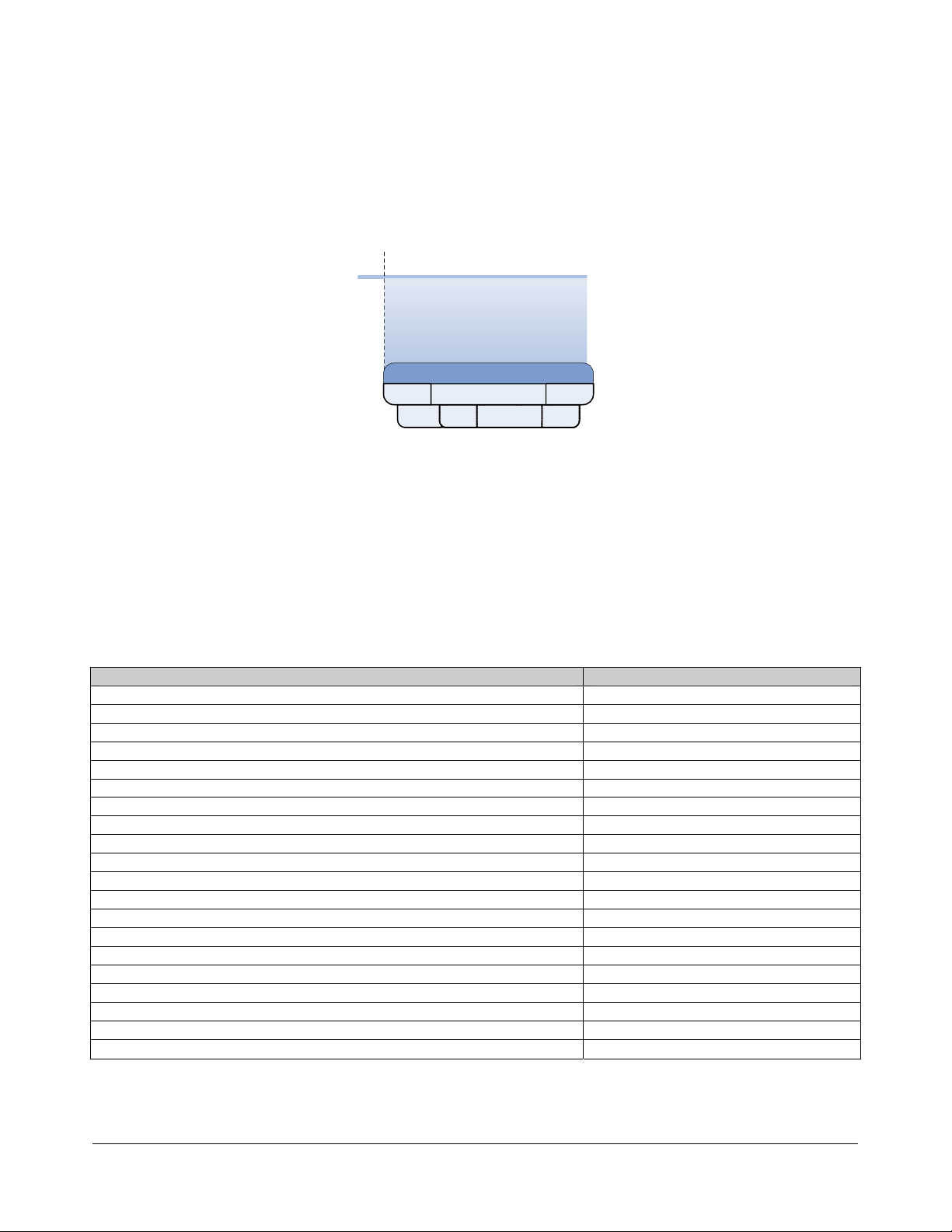
2.2 OCHI USB 1.1 and EHCI USB 2.0 Controllers
Note: Some USB functions are controlled by, and associated with, certain PCI configuration registers in the
SMBus/ACPI device. For more information refer to section 2.3: SMBus Module and ACPI Block (Device 20,
Function 0). The diagram below lists these USB functions and the associated registers.
USB
OHCI / EHCI Controller Enables
USB Reset / PowerDown
USB Legacy control
USB Smart Power Control
USB PM & SMI Control
PCI_Reg:
AD:AC
AD:AC
ACh 3Ch
2.2.1 OHCI Registers (Device 19, Function 0, 1, 2, 3, 4)
2.2.1.1 PCI Configuration Registers (PCI_Reg)
61/64/65/68/6Bh
0Fh
78h BEh
5B/5Ch
There are 5 Open-HCI compatible USB host controllers present (functions 0, 1, 2, 3, and 4), and each has
their own set of registers. This section describes the configuration registers necessary for the OpenHCIcompliant USB Host Controllers to interface with other system components in a PCI-based PC host. These
registers are accessed for set-up during PCI initialization or through special cycles during normal system
runtime. Below is summary of the registers that are necessary for the OpenHCI-compliant USB Host
Controller to be successfully configured in a PCI-based PC host.
OHCI0 – PCI config
Register Name Offset Address
Device / Vendor ID 00h
Command 04h
Status 06h
Revision ID / Class Code 08h
Miscellaneous 0Ch
BAR_OHCI 10h
Subsystem Vendor ID / Subsystem ID 2Ch
Capability Pointer 34h
Interrupt Line 3Ch
Config Timers / MSI Disable 40h – 41h
Port Disable Control 42h – 43h
OHCI Misc Control 50h
Over Current Control 1 58h
Over Current Control 2 5Ch
OHCI OverCurrent Enable 68h – 69h
Target Timeout Control 74h
MSI Control D0h
MSI Address D4h
MSI Data D8h
HT MSI Support E4h
OHCI1/2/3/4 – PCI config
©2008 Advanced Micro Devices, Inc.
OCHI USB 1.1 and EHCI USB 2.0 Controllers
AMD SB600 Register Reference Manual Proprietary Page 44
Page 45

Register Name Offset Address
Device / Vendor ID 00h
Command 04h
Status 06h
Revision ID / Class Code 08h
Miscellaneous 0Ch
BAR_OHCI 10h
Subsystem Vendor ID / Subsystem ID 2Ch
Capability Pointer 34h
Interrupt Line 3Ch
MSI Control D0h
MSI Address D4h
MSI Data D8h
Figure 3 PCI Configuration Spaces for OHCI
There are 5 OHCI compatible USB host controllers present (functions 0, 1, 2, 3 and 4), and each has their
own set of registers.
Device / Vendor ID – R - 32 bits - [PCI_Reg : 00h]
Field Name Bits Default Description
VEND_ID 15:0 1002h Vendor ID
©2008 Advanced Micro Devices, Inc.
AMD SB600 Register Reference Manual Proprietary Page 45
OCHI USB 1.1 and EHCI USB 2.0 Controllers
Page 46

Device / Vendor ID – R - 32 bits - [PCI_Reg : 00h]
Field Name Bits Default Description
DEV_ID 31:16 Function 0: 4387h
Function 1: 4388h
Function 2: 4389h
Function 3: 438Ah
Function 4: 438Bh
Device ID
Command – RW - 16 bits - [PCI_Reg : 04h]
Field Name Bits Default Description
IO Space
Accesses
Memory Space
Accesses
Bus Master 2 0b A value of 0 disables the device from generating PCI accesses.
Special Cycle 3 0b Hard-wired to 0, indicating no Special Cycle support.
Memory Write
and Invalidate
Command
VGA Palette
Register
Accesses
Parity Enable 6 0b When it is 1, the device must take its normal action when a parity error is
Reserved 7 0b Hard-wired to 0 per PCI2.3 spec.
SERR# Enable 8 0b A value of 0 disables the SERR# driver.
Fast Back-toBack Enable
Interrupt Disable 10 0b A value of 0 enables the assertion of the device/function’s INTx# signal.
Reserved 15:11 Reserved
0 0b A value of 0 disables the device response.
A value of 1 allows the device to respond to I/O Space accesses.
1 0b A value of 0 disables the device response.
A value of 1 allows the device to respond to Memory Space accesses.
A value of 1 allows the device to behave as a bus master.
4 0b When it is 0, Memory Write must be used.
When it is 1, masters may generate the command.
5 0b Hard-wired to 0, indicating the device should treat palette write accesses
like all other accesses.
detected.
When it is 0, the device sets its Detected Parity Error status bit (bit 15 in
the Status register) when an error is detected, but continues normal
operations without asserting PERR#.
A value of 1 enables the SERR# driver.
Address parity errors are reported only if this bit and bit [6] are 1.
9 0b A value of 0 means that only fast back-to-back transactions to the same
agent are allowed.
A value of 1 means the master is allowed to generate fast back-to-back
transactions to different agents.
A value of 1 disables the assertion of the device/function’s INTx# signal.
Status – R - 16 bits - [PCI_Reg : 06h]
Field Name Bits Default Description
Reserved 2:0 Reserved
Interrupt Status 3 0b This bit reflects the state of the interrupt in the device/function. Only
when the Interrupt Disable bit in the command register is a 0 and this
Interrupt Status bit is a 1 will the device’s/function’s INTx# signal be
asserted. Setting the Interrupt Disable bit to a 1 has no effect on the
state of this bit.
Capabilities List 4 1b A value of 0 indicates that no New Capabilities linked list is available.
A value of 1 indicates that the value read at offset 34h is a pointer in
Configuration Space to a linked list of new capabilities.
66 MHz Capable 5 1b Hard-wired to 1, indicating 66MHz capable.
Reserved 6 Reserved
Fast Back-toBack Capable
©2008 Advanced Micro Devices, Inc.
7 1b Hard-wired to 1, indicating Fast Back-to-Back capable.
OCHI USB 1.1 and EHCI USB 2.0 Controllers
AMD SB600 Register Reference Manual Proprietary Page 46
Page 47

Status – R - 16 bits - [PCI_Reg : 06h]
Field Name Bits Default Description
Master Data
Parity Error
DEVSEL timing 10:9 01b Hard-wired to 01b – medium timing
Signaled Target
Abort
Received Target
Abort
Received Master
Abort
Signaled System
Error
Detected Parity
Error
8 0b This bit is set only when three conditions are met: 1) the bus agent
asserted PERR# itself (on a read) or observed PERR# asserted (on a
write); 2) the agent setting the bit acted as the bus master for the
operation in which the error occurred; and 3) the Parity Error Response
bit (Command register) is set.
11 0b This bit is set by a target device whenever it terminates a transaction
with Target-Abort.
12 0b This bit is set by a master device whenever its transaction is terminated
with Target-Abort.
13 0b This bit is set by a master device whenever its transaction (except for
Special Cycle) is terminated with Master-Abort.
14 0b This bit is set whenever the device asserts SERR#.
15 0b This bit is set by the device whenever it detects a parity error, even if
parity error handling is disabled (as controlled by bit 6 in the Command
register).
Revision ID / Class Code – R - 32 bits - [PCI_Reg : 08h]
Field Name Bits Default Description
Revision ID 7:0 00h Revision ID.
PI 15:8 10h Programming Interface. A constant value of ‘10h’ indentifies the device
being an OpenHCI Host Controller.
SC 23:16 03h Sub Class. A constant value of ‘03h’ indentifies the device being of
Universal Serial Bus.
BC 31:24 0Ch Base Class. A constant value of ‘0Ch’ identifies the device being a Serial
Bus Controller.
Miscellaneous – RW/R - 32 bits - [PCI_Reg : 0Ch]
Field Name Bits Default Description
Cache Line Size 7:0 00h This read/write field specifies the system cacheline size in units of
DWORDs and must be initialized to 00h.
Latency Timer 15:8 00h [9:8] hard-wired to 00b, resulting in a timer granularity of at least four
clocks. This field specifies, in units of PCI bus clocks, the value of the
Latency Timer for this PCI bus master.
Header Type 23:16 80h/00h This field identifies the layout of the second part of the predefined header
(beginning at byte 10h in Configuration Space) and also whether or not
the device contains multiple functions.
Function 0: Bit[23] hard-wired to 1 Æ the device has multiple functions.
Function 1: Bit[23] hard-wired to 0 Æ the device is single function.
Function 2: Bit[23] hard-wired to 0 Æ the device is single function.
Function 3: Bit[23] hard-wired to 0 Æ the device is single function.
Function 4: Bit[23] hard-wired to 0 Æ the device is single function.
Bits [22:16] are hard-wired to 00h.
BIST 31:24 00h Hard-wired to 00h, indicating no build-in BIST support.
Bar_OHCI – RW - 32 bits - [PCI_Reg : 10h]
Field Name Bits Default Description
IND 0 0b Indicator. A constant value of ‘0’ indicates that the operational registers
of the device are mapped into memory space of the main memory of the
PC host system. Read Only.
TP 2:1 0h Type. A constant value of ‘00b’ indicates that the base register is 32-bit
wide and can be placed anywhere in the 32-bit memory space; i.e., lower
4 GB of the main memory of the PC host. Read Only.
©2008 Advanced Micro Devices, Inc.
OCHI USB 1.1 and EHCI USB 2.0 Controllers
AMD SB600 Register Reference Manual Proprietary Page 47
Page 48

Bar_OHCI – RW - 32 bits - [PCI_Reg : 10h]
Field Name Bits Default Description
PM 3 0b Prefetch memory. A constant value of ‘0’ indicates that there is no
support for “prefetchable memory”. Read Only.
11:4 00h Represents a maximum of 4-KB addressing space for the OpenHCi’s
operational registers. Read Only.
BAR 31:12 000h Base Address. Specifies the upper 20 bits of the 32-bit starting base
address. This represent a maximum of 4-KB addressing space for the
OpenHCI’s operational registers.
Subsystem Vendor ID / Subsystem ID – RW - 32 bits - [PCI_Reg : 2Ch]
Field Name Bits Default Description
Subsystem Vendor ID 15:0 0000h Can only be written once by software.
Subsystem ID 31:16 0000h Can only be written once by software.
Capability Pointer – R - 8 bits - [PCI_Reg : 34h]
Field Name Bits Default Description
Capability Pointer 7:0 D0h Address of the 1st element of capability link.
Interrupt Line – RW – 32 bits - [PCI_Reg : 3Ch]
Field Name Bits Default Description
Interrupt Line 7:0 00h The Interrupt Line register is an eight-bit register used to
communicate interrupt line routing information. The register
is read/write and must be implemented by any device (or
device function) that uses an interrupt pin. POST software
will write the routing information into this register as it
initializes and configures the system.
The value in this register tells which input of the system
interrupt controller(s) the device's interrupt pin is connected
to. The device itself does not use this value; rather it is used
by device drivers and operating systems. Device drivers
and operating systems can use this information to determine
priority and vector information. Values in this register are
system architecture specific.
Interrupt Pin 15:8
01h
02h
03h
02h
03h
MIN_GNT 23:16 00h Read Only. Hardwired to 00h to indicate no major
MAX_LAT 31:24 00h Read Only. Hardwired to 00h to indicate no major
Read Only by default.
OHCI0: Hard-wired to 01h, corresponding to using INTA#.
OHCI1: Hard-wired to 02h, corresponding to using INTB#.
OHCI2: Hard-wired to 03h, corresponding to using INTC#.
OHCI3: Hard-wired to 02h, corresponding to using INTB#.
OHCI4: Hard-wired to 03h, corresponding to using INTC#.
requirements for the settings of Latency Timers.
requirements for the settings of the Latency Timers.
Config Timers / MSI Disable (OHCI0 only) – RW - 16 bits - [PCI_Reg : 40h]
Field Name Bits Default Description
TRDY Timer 7:0 80h Target Ready timer to timeout non-responding target.
©2008 Advanced Micro Devices, Inc.
OCHI USB 1.1 and EHCI USB 2.0 Controllers
AMD SB600 Register Reference Manual Proprietary Page 48
Page 49

Config Timers / MSI Disable (OHCI0 only) – RW - 16 bits - [PCI_Reg : 40h]
Field Name Bits Default Description
MSI Disable 12:8 00h When these bits are set MSI capability will be disabled for
the corresponding Host Controller.
Bit 8 – OHCI0
Bit 9 – OHCI1
Bit 10 – OHCI2
Bit 11 – OHCI3
Bit 12 – OHCI4
Reserved 15:13 0h Reserved
Port Disable (OHCI0 only) – RW - 16 bits - [PCI_Reg : 42h]
Field Name Bits Default Description
Port_disable 9:0 00h When these bits are set the corresponding ports are
disabled. For example, if bit-0 is set, then port-0 (its
corresponding port) is disabled; if bit-1 is set, then its
corresponding port (port-1) is disabled (and so on).
Reserved 15:10 00h Reserved
OHCI Misc Control (OHCI0 only) – RW - 16 bits - [PCI_Reg: 50h]
Field Name Bits Default Description
Reserved 7:0 00h Reserved.
DisUsbS3OvrCur 8 0b Set to 1 to disable over-current detection for both EHCII and
OHCI.
Reserved 9 0b Reserved.
OHCI Cache Enable 10 1b Enable bit for 64 byte OHCI DMA cache.
OHCI Prefetch Enable 11 1b Enable bit to prefetch next cache line for OHCI DMA reads.
SMI Handshake Disable 12 0b If this bit is set the Handshake between USB and ACPI is
disabled when SMI is requested by USB
Reserved 15: 13 0h Reserved.
Over Current Control 1 (OHCI0 only) – R - 32 bits - [PCI_Reg : 58h]
Field Name Bits Default Description
Port0 OverCurrent Control 3:0 Fh The register is to control the OverCurrent pin mapping for
Port-0. There are 10 OverCurrent pins (USB_OC0 ~
USB_OC9), any value greater than 0x9h will disable the
OverCurrent function for port-0.
Port1 OverCurrent Control 7:4 Fh The register is to control the OverCurrent pin mapping for
Port-1. There are 10 OverCurrent pins (USB_OC0 ~
USB_OC9), any value greater than 0x9h will disable the
OverCurrent function for port-1.
Port2 OverCurrent Control 11:8 Fh The register is to control the OverCurrent pin mapping for
Port-2. There are 10 OverCurrent pins (USB_OC0 ~
USB_OC9), any value greater than 0x9h will disable the
OverCurrent function for port-2.
Port3 OverCurrent Control 15:12 Fh The register is to control the OverCurrent pin mapping for
Port-3. There are 10 OverCurrent pins (USB_OC0 ~
USB_OC9), any value greater than 0x9h will disable the
OverCurrent function for port-3.
Port4 OverCurrent Control 19:16 Fh The register is to control the OverCurrent pin mapping for
Port-4. There are 10 OverCurrent pins (USB_OC0 ~
USB_OC9), any value greater than 0x9h will disable the
OverCurrent function for port-4.
©2008 Advanced Micro Devices, Inc.
OCHI USB 1.1 and EHCI USB 2.0 Controllers
AMD SB600 Register Reference Manual Proprietary Page 49
Page 50

Over Current Control 1 (OHCI0 only) – R - 32 bits - [PCI_Reg : 58h]
Field Name Bits Default Description
Port5 OverCurrent Control 23:20 Fh The register is to control the OverCurrent pin mapping for
Port-5. There are 10 OverCurrent pins (USB_OC0 ~
USB_OC9), any value greater than 0x9h will disable the
OverCurrent function for port-5.
Port6 OverCurrent Control 27:24 Fh The register is to control the OverCurrent pin mapping for
Port-6. There are 10 OverCurrent pins (USB_OC0 ~
USB_OC9), any value greater than 0x9h will disable the
OverCurrent function for port-6.
Port7 OverCurrent Control 31:28 Fh The register is to control the OverCurrent pin mapping for
Port-7. There are 10 OverCurrent pins (USB_OC0 ~
USB_OC9), any value greater than 0x9h will disable the
OverCurrent function for port-7.
There are 10 pins can be used as USB OverCurrent function –
USB_OC0#/GPM0# USB_OC1#/GPM1# USB_OC2#/GPM2# USB_OC3#/GPM3#
USB_OC4#/GPM4# USB_OC5#/GPM5# USB_OC6#/GEVENT6# USB_OC7#/GEVENT7#
USB_OC8#/GPM8# USB_OC9#/SLP_S2/GPM9#
Register value-to-OverCurrent Pin mapping:
USB_OC0# = 0000, USB_OC1# = 0001, USB_OC2# = 0010, USB_OC3# = 0011,
USB_OC4# = 0100, USB_OC5# = 0101, USB_OC6# = 0110, USB_OC7# = 0111,
USB_OC8# = 1000, USB_OC9# = 1001
* Note: Since OverCurrent pins can be used as GPM# as well, the corresponding register bits to set the pin as
OverCurrent have to be set in Smbus Controller.
Over Current Control 2 (OHCI0 only) – R - 32 bits - [PCI_Reg : 5Ch]
Field Name Bits Default Description
Port8 OverCurrent Control 3:0 Fh The register is to control the OverCurrent pin mapping for
Port-8. There are 10 OverCurrent pins (USB_OC0 ~
USB_OC9), any value greater than 0x9h will disable the
OverCurrent function for port-8.
Port9 OverCurrent Control 7:4 Fh The register is to control the OverCurrent pin mapping for
Port-9. There are 10 OverCurrent pins (USB_OC0 ~
USB_OC9), any value greater than 0x9h will disable the
OverCurrent function for port-9.
Reserved 31:8 Reserved
There are 10 pins can be used as USB OverCurrent function –
USB_OC0#/GPM0# USB_OC1#/GPM1# USB_OC2#/GPM2# USB_OC3#/GPM3#
USB_OC4#/GPM4# USB_OC5#/GPM5# USB_OC6#/GEVENT6# USB_OC7#/GEVENT7#
USB_OC8#/GPM8# USB_OC9#/SLP_S2/GPM9#
Register value-to-OverCurrent Pin mapping:
USB_OC0# = 0000, USB_OC1# = 0001, USB_OC2# = 0010, USB_OC3# = 0011,
USB_OC4# = 0100, USB_OC5# = 0101, USB_OC6# = 0110, USB_OC7# = 0111,
USB_OC8# = 1000, USB_OC9# = 1001
*Note: Since OverCurrent pins can be used as GPM# as well, the corresponding register bits to set the pin as
OverCurrent have to be set in Smbus Controller.
OHCI OverCurrent Enable (OHCI0 only) – RW - 16 bits - [PCI_Reg : 68h]
Field Name Bits Default Description
OHCI OverCurrent Enable 9:0 00h Writing this bit to a one enables the respective port to be
sensitive to over-current conditions as wake-up events when
it is owned by OHCI.
Reserved 15:10 00h Reserved
©2008 Advanced Micro Devices, Inc.
OCHI USB 1.1 and EHCI USB 2.0 Controllers
AMD SB600 Register Reference Manual Proprietary Page 50
Page 51

Target Timeout Control (OHCI0 only) – RW - 32 bits - [PCI_Reg : 74h]
Field Name Bits Default Description
Retry counter 7:0 FFh Counter to control the purge of the delay queue when the
host controller does not return the ack. After the counter
expires the transaction is target aborted.
The retry counter can be disabled by writing 00h in this
Register.
Reserved 23:8 0000h Reserved
Timeout Timer 31:24 80h Timer to control the purge of the delay queue when the
master that has initiated the access does not return to
complete the transaction. After the timer expires the queue
is invalidated and the next transaction is serviced.
MSI Control – RW - 32 bits - [PCI_Reg : D0h]
Field Name Bits Default Description
MSI USB 7:0 05h MSI USB ID. Read only.
Next Item Pointer 15:8 00h Pointer to next capability structure
MSI Control Out 16 0b Set to 1 to disable IRQ. Use MSI instead.
Reserved 19:17 0h Reserved
MSI Control 22:20 0h MSI control field
Reserved 31:23 00h Reserved
MSI Address – RW - 32 bits - [PCI_Reg : D4h]
Field Name Bits Default Description
MSI Address 31:0 0h System-specified message address.
MSI Data – RW - 16 bits - [PCI_Reg : D8h]
Field Name Bits Default Description
MSI Data 15:0 0h System-specified message.
2.2.1.2 OHCI Operational Registers (MEM_Reg)
The Host Controller (HC) contains a set of on-chip operational registers, which are mapped into a noncacheable portion of the system addressable space. These registers are used by the Host Controller Driver
(HCD) and should be read and written as Dwords.
Reserved bits may be allocated in future releases and should not be assumed to contain 0. The Host
Controller Driver should always preserve the value(s) of the reserved field. When a write to set/clear register
is written, bits written to reserved fields should be 0.
Register Name Offset Address
HcRevision 0h
HcControl 4h
HcCommandStatus 8h
HcInterruptStatus Ch
HcInterruptEnable 10h
HcInterruptDisable 14h
HcHCCA 18h
HcPeriodCurrentED 1Ch
HcControlHeadED 20h
HcControlCurrentED 24h
HcBulkHeadED 28h
©2008 Advanced Micro Devices, Inc.
OCHI USB 1.1 and EHCI USB 2.0 Controllers
AMD SB600 Register Reference Manual Proprietary Page 51
Page 52

Register Name Offset Address
HcBulkCurrentED 2Ch
HcDoneHead 30h
HcFmInterval 34h
HcFmRemaining 38h
HcFmNumber 3Ch
HcPeriodicStart 40h
HcLSThreshold 44h
HcRhDescriptorA 48h
HcRhDescriptorB 4Ch
HCRhStatus 50h
HcRhPortStatus[1] 54h
… …
HcRhPortStatus[NDP] 54+4*NDP
HcRevision – R - 32 bits - [MEM_Reg : 00h]
Field Name Bits Default Description
REV 7:0 10h
L 8 1b
Reserved 31:9 Reserved
Revision.
This read-only field contains the version of HCI specification.
Legacy
This read-only field is 1, indicating that the legacy support registers are
present in this HC.
HcControl - 32 bits - [MEM_Reg : 04h]
Field Name Bits Default HCD HC Description
CBSR 1:0 00b RW R
ControlBulkServiceRatio
This specifies the service ratio between Control and
Bulk Eds. Before processing any of the non-periodic
lists, HC must compare the ratio specified with its
internal count on how many nonempty Control Eds
have been processed, in determining whether to
continue serving another Control ED or switching to
Bulk Eds.
No. of Control Eds Over Bulk Eds Served
PLE 2 0b RW R
PeriodicListEnable
This bit is set to enable the processing of the periodic
list in the next Frame. If cleared by HCD, processing
of the periodic list does not occur after the next SOF.
HC must check this bit before it starts processing the
list.
CBSR
0
1:1
1
2:1
2
3:1
3
4:1
©2008 Advanced Micro Devices, Inc.
OCHI USB 1.1 and EHCI USB 2.0 Controllers
AMD SB600 Register Reference Manual Proprietary Page 52
Page 53

HcControl - 32 bits - [MEM_Reg : 04h]
Field Name Bits Default HCD HC Description
IE 3 0b RW R
CLE 4 0b RW R
BLE 5 0b RW R
HCFS 7:6 00b RW RW
IsochronousEnable
This bit is used by HCD to enable/disable processing
of isochronous Eds. While processing the periodic list
in a Frame, HC checks he status of this bit when it
finds an Isochronous ED (F=1). If set (enabled), HC
continues processing the Eds. If cleared (disabled),
HC halts processing of the periodic list (which now
contains only isochronous Eds) and begins
processing the Bulk/Control lists. Setting this bit is
guaranteed to take effect in the next Frame (not the
current Frame).
ControlListEnable
This bit is set to enable the processing of the Control
list in the next Frame. If cleared by HCD, processing
of the Control list does not occur after the next SOF.
HC must check this bit whenever it determines to
process the list. When disabled, HCD may modify the
list. If HcControlCurrentED is pointing to an ED to be
removed, HCD must advance the pointer by updating
HcControlCurrentED before re-enabling processing of
the list.
BulkListEnable
This bit is set to enable the processing of the Bulk list
in the next Frame. If cleared by HCD, processing of
the Bulk list does not occur after the next SOF. HC
checks this bit whenever it determines to process the
list. When disabled, HCD may modify the list. If
HcBulkCurrentED is pointing to an ED to be removed,
HCD must advance the pointer by updating
HcBulkCurrentED before re-enabling processing of
the list.
HostControllerFunctionalState for USB
00b: U
SBRESET
01b: USBRESUME
10b: USBOPERATIONAL
11b: USBSUSPEND
A transition to USBOPERATIONAL from another
state causes SOF generation to begin 1 ms
later. HCD may determine whether HC has
begun sending SOFs by reading the
StartofFrame field of HcInterruptStatus.
This field may be changed by HC only when in
the U
SBSUSPEND state. HC may move from the
USBSUSPEND state to the USBRESUME state after
detecting the resume signaling from a
downstream port.
HC enters U
whereas it enters U
SBSUSPEND after a software reset,
SBRESET after a hardware
reset. The latter also resets the Root Hub and
asserts subsequent reset signaling to
downstream ports.
©2008 Advanced Micro Devices, Inc.
OCHI USB 1.1 and EHCI USB 2.0 Controllers
AMD SB600 Register Reference Manual Proprietary Page 53
Page 54

HcControl - 32 bits - [MEM_Reg : 04h]
Field Name Bits Default HCD HC Description
IR 8 0b RW R
RWC 9 0b RW RW
RWE 10 0b RW R
Reserved 31:11
InterruptRouting
This bit determines the routing of interrupts generated
by events registered in HcInterruptStatus. If clear, all
interrupts are routed to the normal host bus interrupt
mechanism. If set, interrupts are routed to the System
Management Interrupt. HCD clears this bit upon a
hardware reset, but it does not alter this bit upon a
software reset. HCD uses this bit as a tag to indicate
the ownership of HC.
RemoteWakeupConnected
This bit indicates whether HC supports remote
wakeup signaling. If remote wakeup is supported and
used by the system it is the responsibility of system
firmware to set this bit during POST. HC clears the bit
upon a hardware reset but does not alter it upon a
software reset. Remote wakeup signaling of the host
system is host-bus-specific and is not described in
this specification.
RemoteWakeupEnable
This bit is used by HCD to enable or disable the
remote wakeup feature upon the detection of
upstream resume signaling. When this bit is set and
the ResumeDetected bit in HcInterruptStatus is set, a
remote wakeup is signaled to the host system.
Setting this bit has no impact on the generation of
hardware interrupt.
Reserved
HcCommandStatus - 32 bits - [MEM_Reg : 08h]
Field Name Bits Default HCD HC Description
HCR 0 0b RW RW
HostControllerReset
This bit is set by HCD to initiate a software reset of
HC.Regardless of the functional state of HC, it moves
to the
USBSUSPEND state in which most of the
operational registers are reset except those stated
otherwise; e.g., the InterruptRouting field of
HcControl, and no Host bus accesses are allowed.
This bit is cleared by HC upon the completion of the
reset operation. The reset operation must be
completed within 10 ms. This bit, when set, should
not cause a reset to the Root Hub and no subsequent
reset signaling should be asserted to its downstream
ports.
©2008 Advanced Micro Devices, Inc.
OCHI USB 1.1 and EHCI USB 2.0 Controllers
AMD SB600 Register Reference Manual Proprietary Page 54
Page 55

HcCommandStatus - 32 bits - [MEM_Reg : 08h]
Field Name Bits Default HCD HC Description
CLF 1 0b RW RW
BLF 2 0b RW RW
OCR 3 0b RW RW
Reserved 15:4
SOC 17:16 00b R RW
Reserved 31:18 Reserved
ControlListFilled
This bit is used to indicate whether there are any TDs
on the Control list. It is set by HCD whenever it adds
a TD to an ED in the Control list. When HC begins to
process the head of the Control list, it checks CLF. As
long as ControlListFilled is 0, HC will not start
processing the Control list. If CF is 1, HC will start
processing the Control list and will set
ControlListFilled to 0. If HC finds a TD on the list,
then HC will set ControlListFilled to 1 causing
the Control list processing to continue. If no TD is
found on the Control list, and if the HCD does not set
ControlListFilled, then ControlListFilled will still be 0
when HC completes processing the Control list and
Control list processing will stop.
BulkListFilled
This bit is used to indicate whether there are any TDs
on the Bulk list. It is set by HCD whenever it adds a
TD to an ED in the Bulk list. When HC begins to
process the head of the Bulk list, it checks BF. As
long as BulkListFilled is 0, HC will not start
processing the Bulk list. If BulkListFilled is 1, HC will
start processing the Bulk list and will set BF to 0. If
HC finds a TD on the list, then HC will set
BulkListFilled to 1 causing the Bulk list processing to
continue. If no TD is found on the Bulk list, and if
HCD does not set BulkListFilled, then BulkListFilled
will still be 0 when HC completes processing the Bulk
list and Bulk list processing will stop. BulkListFilled
This bit is used to indicate whether there are any TDs
on the Bulk list. It is set by HCD whenever it adds a
TD to an ED in the Bulk list. When HC begins to
process the head of the Bulk list, it checks BF. As
long as BulkListFilled is 0, HC will not start
processing the Bulk list. If BulkListFilled is 1, HC will
start processing the
Bulk list and will set BF to 0. If HC finds a TD on the
list, then HC will set BulkListFilled to 1 causing the
Bulk list processing to continue. If no TD is found on
the Bulk list, and if HCD does not set BulkListFilled,
then BulkListFilled will still be 0 when HC completes
processing the Bulk list and Bulk list processing will
stop.
OwnershipChangeRequest
This bit is set by an OS HCD to request a change of
control of the HC. When set HC will set the
OwnershipChange field in HcInterruptStatus. After
the changeover, this bit is cleared and remains so
until the next request from OS HCD.
SchedulingOverrunCount
These bits are incremented on each scheduling
overrun error. It is initialized to 00b and wraps around
at 11b. This will be incremented when a scheduling
overrun is detected even if SchedulingOverrun in
HcInterruptStatus has already been set. This is used
by HCD to monitor any persistent scheduling
problems.
©2008 Advanced Micro Devices, Inc.
OCHI USB 1.1 and EHCI USB 2.0 Controllers
AMD SB600 Register Reference Manual Proprietary Page 55
Page 56

HcInterruptStatus – RW - 32 bits - [MEM_Reg : 0Ch]
Field Name Bits Default HCD HC Description
SO 0 0b RW RW
WDH 1 0b RW RW
SF 2 0b RW RW
RD 3 0b RW RW
UE 4 0b RW RW
FNO 5 0b RW RW
RHSC 6 0b RW RW
Reserved 29:7 Reserved
OC 30 0b RW RW
Reserved 31 Reserved
SchedulingOverrun
This bit is set when the USB schedule for the current
Frame overruns and after the update of
HccaFrameNumber. A scheduling overrun will also
cause the SchedulingOverrunCount of
HcCommandStatus to be incremented.
WritebackDoneHead
This bit is set immediately after HC has written
HcDoneHead to HccaDoneHead. Further updates of
the HccaDoneHead will not occur until this bit has
been cleared. HCD should only clear this bit after it
has saved the content of HccaDoneHead.
StartofFrame
This bit is set by HC at each start of a frame and after
the update of HccaFrameNumber. HC also generates
a SOF token at the same time.
ResumeDetected
This bit is set when HC detects that a device on the
USB is asserting resume signaling. It is the transition
from no resume signaling to resume signaling
causing this bit to be set. This bit is not set when
HCD sets the
UnrecoverableError
This bit is set when HC detects a system error not
related to USB. HC should not proceed with any
processing nor signaling before the system error has
been corrected. HCD clears this bit after HC has
been reset.
FrameNumberOverflow
This bit is set when the MSb of HcFmNumber (bit 15)
changes value, from 0 to 1 or from 1 to 0, and after
HccaFrameNumber has been updated.
RootHubStatusChange
This bit is set when the content of HcRhStatus or the
content of any of HcRhPortStatus
[NumberofDownstreamPort] has changed.
OwnershipChange
This bit is set by HC when HCD sets the
OwnershipChangeRequest field in
HcCommandStatus. This event, when unmasked, will
always generate an System Management Interrupt
(SMI) immediately.
This bit is tied to 0b when the SMI pin is not
implemented.
USBRESUME state.
HcInterruptEnable - 32 bits - [MEM_Reg : 10h]
Field Name Bits Default HCD HC Description
SO 0 0b RW RW 0 - Ignore
1 - Enable interrupt generation due to Scheduling
Overrun.
WDH 1 0b RW RW 0 - Ignore
1 - Enable interrupt generation due to HcDoneHead
Writeback.
SF 2 0b RW RW 0 - Ignore
1 - Enable interrupt generation due to Start of Frame.
©2008 Advanced Micro Devices, Inc.
OCHI USB 1.1 and EHCI USB 2.0 Controllers
AMD SB600 Register Reference Manual Proprietary Page 56
Page 57

HcInterruptEnable - 32 bits - [MEM_Reg : 10h]
Field Name Bits Default HCD HC Description
RD 3 0b RW W 0 - Ignore
1 - Enable interrupt generation due to Resume
Detect.
UE 4 0b RW RW 0 - Ignore
1 - Enable interrupt generation due to Unrecoverable
Error.
FNO 5 0b RW RW 0 - Ignore
1 - Enable interrupt generation due to Frame Number
Overflow.
RHSC 6 0b RW RW 0 - Ignore
1 - Enable interrupt generation due to Root Hub
Status Change.
Reserved 29:7 Reserved
OC 30 0b RW RW 0 - Ignore
1 - Enable interrupt generation due to Ownership
Change.
MIE 31 0b RW R A ‘0’ written to this field is ignored by HC. A '1' written
to this field enables interrupt generation due to events
specified in the other bits of this register. This is used
by HCD as a Master Interrupt Enable.
HcInterruptDisable - 32 bits - [MEM_Reg : 14h]
Field Name Bits Default HCD HC Description
SO 0 0b RW R 0 - Ignore
1 - Disable interrupt generation due to Scheduling
Overrun.
WDH 1 0b RW R 0 - Ignore
1 - Disable interrupt generation due to HcDoneHead
Writeback.
SF 2 0b RW R 0 - Ignore
1 - Disable interrupt generation due to Start of Frame.
RD 3 0b RW R 0 - Ignore
1 - Disable interrupt generation due to Resume
Detect.
UE 4 0b RW R 0 - Ignore
1 - Disable interrupt generation due to Unrecoverable
Error.
FNO 5 0b RW R 0 - Ignore
1 - Disable interrupt generation due to Frame Number
Overflow.
RHSC 6 0b RW R 0 - Ignore
1 - Disable interrupt generation due to Root Hub
Status Change.
Reserved 29:7 Reserved
OC 30 0b RW R 0 - Ignore
1 - Disable interrupt generation due to Ownership
Change.
MIE 31 0b RW R A '0' written to this field is ignored by HC. A '1' written
to this field disables interrupt generation due to
events specified in the other bits of this register. This
field is set after a hardware or software reset.
HcHCCA - 32 bits - [MEM_Reg : 18h]
Field Name Bits Default HCD HC Description
Reserved 7:0 Reserved
HCCA 31:8 000000h RW R This is the base address of the Host Controller
Communication Area
©2008 Advanced Micro Devices, Inc.
OCHI USB 1.1 and EHCI USB 2.0 Controllers
AMD SB600 Register Reference Manual Proprietary Page 57
Page 58

HcPeriodCurrentED - 32 bits - [MEM_Reg : 1Ch]
Field Name Bits Default HCD HC Description
Reserved 3:0 Reserved
PCED 31:4 0000000
h
R RW
PeriodCurrentED
This is used by HC to point to the head of one of the
Periodic lists which will be processed in the current
Frame. The content of this register is updated by HC
after a periodic ED has been processed. HCD may
read the content in determining which ED is currently
being processed at the time of reading.
HcControlHeadED- 32 bits - [MEM_Reg : 20h]
Field Name Bits Default HCD HC Description
Reserved 3:0 Reserved
CHED 31:4 0000000h RW R
ControlHeadED
HC traverses the Control list starting with the
HcControlHeadED pointer. The content is loaded
from HCCA during the initialization of HC.
HcControlCurrentED - 32 bits - [MEM_Reg : 24h]
Field Name Bits Default HCD HC Description
Reserved 3:0 Reserved
CCED 31:4 0000000h RW RW
ControlCurrentED
This pointer is advanced to the next ED after serving
the present one. HC will continue processing the list
from where it left off in the last Frame. When it
reaches the end of the Control list, HC checks the
ControlListFilled of in HcCommandStatus. If set, it
copies the content of HcControlHeadED to
HcControlCurrentED and clears the bit. If not set, it
does nothing. HCD is allowed to modify this register
only when the ControlListEnable of HcControl is
cleared. When set, HCD only reads the
instantaneous value of this register. Initially, this is set
to zero to indicate the end of the Control list.
HcBulkHeadED - 32 bits - [MEM_Reg : 28h]
Field Name Bits Default HCD HC Description
Reserved 3:0 Reserved
BHED 31:4 0b RW R
BulkHeadED
HC traverses the Bulk list starting with the
HcBulkHeadED pointer. The content is loaded from
HCCA during the initialization of HC.
HcBulkCurrentED - 32 bits - [MEM_Reg : 2Ch]
Field Name Bits Default HCD HC Description
Reserved 3:0 Reserved
©2008 Advanced Micro Devices, Inc.
OCHI USB 1.1 and EHCI USB 2.0 Controllers
AMD SB600 Register Reference Manual Proprietary Page 58
Page 59

HcBulkCurrentED - 32 bits - [MEM_Reg : 2Ch]
Field Name Bits Default HCD HC Description
BCED 31:4 0000000h RW RW
BulkCurrentED
This is advanced to the next ED after the HC has
served the present one. HC continues processing the
list from where it left off in the last Frame. When it
reaches the end of the Bulk list, HC checks the
ControlListFilled of HcControl. If set, it copies the
content of HcBulkHeadED to HcBulkCurrentED and
clears the bit. If it is not set, it does nothing. HCD is
only allowed to modify this register when the
BulkListEnable of HcControl is cleared. When set,
the HCD only reads the instantaneous value of this
register. This is initially set to zero to indicate the end
of the Bulk list.
HcDoneHead - 32 bits - [MEM_Reg : 30h]
Field Name Bits Default HCD HC Description
Reserved 3:0 Reserved
DH 31:4 0b R RW
DoneHead
When a TD is completed, HC writes the content of
HcDoneHead to the NextTD field of the TD. HC then
overwrites the content of HcDoneHead with the
address of this TD. This is set to zero whenever HC
writes the content of this register to HCCA. It also
sets the WritebackDoneHead of HcInterruptStatus.
HcFmInterval - 32 bits - [MEM_Reg : 34h]
Field Name Bits Default HCD HC Description
FI 13:0 2EDFh RW R
Reserved 15:14 Reserved
FSMPS 30:16 0000h RW R
FIT 31 0b RW R
FrameInterval
This specifies the interval between two consecutive
SOFs in bit times. The nominal value is set to be
11,999.
HCD should store the current value of this field before
resetting HC. By setting the HostControllerReset
field of HcCommandStatus as this will cause the HC
to reset this field to its nominal value. HCD may
choose to restore the stored value upon the
completion of the Reset sequence.
FSLargestDataPacket
This field specifies a value which is loaded into the
Largest Data Packet Counter at the beginning of
each frame. The counter value represents the largest
amount of data in bits which can be sent or received
by the HC in a single transaction at any given time
without causing scheduling overrun. The field value is
calculated by the HCD.
FrameIntervalToggle
HCD toggles this bit whenever it loads a new value to
FrameInterval
©2008 Advanced Micro Devices, Inc.
OCHI USB 1.1 and EHCI USB 2.0 Controllers
AMD SB600 Register Reference Manual Proprietary Page 59
Page 60

HcFmRemaining - 32 bits - [MEM_Reg : 38h]
Field Name Bits Default HCD HC Description
FR 13:0 0000h R RW
Reserved 30:14 Reserved
FRT 31 0b R RW
FrameRemaining
This counter is decremented at each bit time. When it
reaches zero, it is reset by loading the FrameInterval
value specified in HcFmInterval at the next bit time
boundary. When entering the
state, HC re-loads the content with the
FrameInterval of HcFmInterval and uses the updated
value from the next SOF.
FrameRemainingToggle
This bit is loaded from the FrameIntervalToggle field
of HcFmInterval whenever FrameRemaining
reaches 0. This bit is used by HCD for the
synchronization between FrameInterval and
FrameRemaining.
USBOPERATIONAL
HcFmNumber - 32 bits - [MEM_Reg : 3Ch]
Field Name Bits Default HCD HC Description
FN 15:0 0000h R RW This is incremented when HcFmRemaining is re-
loaded. It will be rolled over to 0h after ffffh. When
entering the
incremented automatically. The content will be written
to HCCA after HC has incremented the
FrameNumber at each frame boundary and sent a
SOF but before HC reads the first ED in that Frame.
After writing to HCCA, HC will set the
StartofFrame in HcInterruptStatus.
Reserved 31:16 Reserved
USBOPERATIONAL state, this will be
HcPeriodicStart - 32 bits - [MEM_Reg : 40h]
Field Name Bits Default HCD HC Description
PS 13:0 0000h RW R
Reserved 31:14
PeriodicStart
After a hardware reset, this field is cleared. This is
then set by HCD during the HC initialization. The
value is calculated roughly as 10% off from
HcFmInterval. A typical value will be 3E67h. When
HcFmRemaining reaches the value specified,
processing of the periodic lists will have priority over
Control/Bulk processing. HC will therefore start
processing the Interrupt list after completing the
current Control or Bulk transaction that is in progress.
Reserved
HcLSThreshold - 32 bits - [MEM_Reg : 44h]
Field Name Bits Default HCD HC Description
LST 11:0 0628h RW R
Reserved 31:12
LSThreshold
This field contains a value which is compared to the
FrameRemaining field prior to initiating a Low Speed
transaction. The transaction is started only if
FrameRemaining this field. The value is calculated
by HCD with the consideration of transmission and
setup overhead.
Reserved
©2008 Advanced Micro Devices, Inc.
OCHI USB 1.1 and EHCI USB 2.0 Controllers
AMD SB600 Register Reference Manual Proprietary Page 60
Page 61

HcRhDescriptorA - 32 bits - [MEM_Reg : 48h]
Field Name Bits Default HCD HC Description
NDP 7:0 02h R R
PSM 8 0b RW R
NPS 9 1b RW R
DT 10 0b R R
OCPM 11 1b RW R
NOCP 12 0b RW R
Reserved 23:13 Reserved
POTPGT 31:24 02h RW R
NumberDownstreamPorts
These bits specify the number of downstream ports
supported by the Root Hub.
PowerSwitchingMode
This bit is used to specify how the power switching of
the Root Hub ports is controlled. It is implementation-
specific. This field is only valid if the
NoPowerSwitching field is cleared.
0: all ports are powered at the same time.
1: each port is powered individually. This mode
allows port power to be controlled by either the global
switch or per-port switching. If the
PortPowerControlMask bit is set, the port responds
only to port power commands
(Set/ClearPortPower). If the port mask is cleared,
then the port is controlled only by the global power
switch (Set/ClearGlobalPower).
NoPowerSwitching
These bits are used to specify whether power
switching is supported or port are always powered. It
is implementation- specific. When this bit is cleared,
the PowerSwitchingMode specifies global or per-
port switching.
0: Ports are power switched
1: Ports are always powered on when the HC is
powered on
DeviceType
This bit specifies that the Root Hub is not a
compound device. The Root Hub is not permitted to
be a compound device. This field should always
read/write 0.
OverCurrentProtectionMode
This bit describes how the overcurrent status for the
Root Hub ports are reported. At reset, this field
should reflect the same mode as
PowerSwitchingMode. This field is valid only if the
NoOverCurrentProtection field is cleared.
0: over-current status is reported collectively for all
downstream ports
1: over-current status is reported on a per-port basis
NoOverCurrentProtection
This bit describes how the overcurrent status for the
Root Hub ports are reported. When this bit is cleared,
the OverCurrentProtectionMode field specifies
global or per-port reporting.
0: Over-current status is reported collectively for all
downstream ports
1: No overcurrent protection supported
PowerOnToPowerGoodTime
This byte specifies the duration HCD has to wait
before accessing a powered-on port of the Root Hub.
It is implementation-specific. The unit of time is 2 ms.
The duration is calculated as POTPGT * 2 ms.
©2008 Advanced Micro Devices, Inc.
OCHI USB 1.1 and EHCI USB 2.0 Controllers
AMD SB600 Register Reference Manual Proprietary Page 61
Page 62

HcRhDescriptorB - 32 bits - [MEM_Reg : 4Ch]
Field Name Bits Default HCD HC Description
DR 15:0 0000h RW R
PPCM 31:16 0000h RW R
DeviceRemovable
Each bit is dedicated to a port of the Root Hub. When
cleared, the attached device is removable. When set,
the attached device is not removable.
bit 0: Reserved
bit 1: Device attached to Port #1
bit 2: Device attached to Port #2
...
bit15: Device attached to Port #15
PortPowerControlMask
Each bit indicates if a port is affected by a global
power control command when
PowerSwitchingMode is set. When set, the port's
power state is only affected by per-port power control
(Set/ClearPortPower). When cleared, the port is
controlled by the global power switch
(Set/ClearGlobalPower). If the device is configured
to global switching mode
(PowerSwitchingMode=0), this field is not valid.
bit 0: Reserved
bit 1: Ganged-power mask on Port #1
bit 2: Ganged-power mask on Port #2
...
bit15: Ganged-power mask on Port #15
HcRhStatus - 32 bits - [MEM_Reg : 50h]
Field Name Bits Default HCD HC Description
LPS 0 0b RW R
OCI 1 0b R RW
Reserved 14:2 Reserved
DRWE 15 0b RW R
(Read) LocalPowerStatus
The Root Hub does not support the local power
status feature; thus, this bit is always read as ‘0’.
(Write) ClearGlobalPower
In global power mode (PowerSwitchingMode=0),
This bit is written to ‘1’ to turn off power to all ports
(Clear)
PortPowerStatus). In per-port power mode, it clears
PortPowerStatus only on ports whose
PortPowerControlMask bit is not set. Writing a ‘0’
has no effect.
OverCurrentIndicator
This bit reports overcurrent conditions when the
global reporting is implemented. When set, an
overcurrent condition exists. When cleared, all power
operations are normal. If per-port overcurrent
protection is implemented this bit is always ‘0’
(Read) DeviceRemoteWakeupEnable
This bit enables a ConnectStatusChange bit as a
resume event, causing a USBSUSPEND to
USBRESUME state transition and setting the
ResumeDetected interrupt.
0 = ConnectStatusChange is not a remote wakeup
event.
1 = ConnectStatusChange is a remote wakeup
event.
(Write) SetRemoteWakeupEnable
Writing a '1' sets DeviceRemoveWakeupEnable.
Writing a '0' has no effect.
©2008 Advanced Micro Devices, Inc.
OCHI USB 1.1 and EHCI USB 2.0 Controllers
AMD SB600 Register Reference Manual Proprietary Page 62
Page 63

HcRhStatus - 32 bits - [MEM_Reg : 50h]
Field Name Bits Default HCD HC Description
LPSC 16 0b RW R
OCIC 17 0b RW RW
Reserved 30:18 Reserved
CRWE 31 - W R
(Read) LocalPowerStatusChange
The Root Hub does not support the local power
status feature; thus, this bit is always read as ‘0’.
(Write) SetGlobalPower
In global power mode (PowerSwitchingMode=0),
This bit is written to ‘1’ to turn on power to all ports
(Clear)
PortPowerStatus). In per-port power mode, it sets
PortPowerStatus only on ports whose
PortPowerControlMask bit is not set. Writing a ‘0’
has no effect.
OverCurrentIndicatorChange
This bit is set by hardware when a change has
occurred to the OCI field of this register. The HCD
clears this bit by writing a ‘1’. Writing a ‘0’ has no
effect.
(Write) ClearRemoteWakeupEnable
Writing a '1' clears DeviceRemoveWakeupEnable.
Writing a '0' has no effect.
HcRhPortStatus - 32 bits - [MEM_Reg : 50h+4*(1:NDP)]
Field Name Bits Default HCD HC Description
CCS 0 0b RW RW
(Read) CurrentConnectStatus
This bit reflects the current state of the downstream
port.
0 = No device connected
1 = Device connected
(Write) ClearPortEnable
The HCD writes a ‘1’ to this bit to clear the
PortEnableStatus bit.
Writing a ‘0’ has no effect. The
CurrentConnectStatus is not affected by any write.
Note: This bit is always read ‘1b’ when the attached
device is non-removable
(DeviceRemoveable[NDP]).
©2008 Advanced Micro Devices, Inc.
OCHI USB 1.1 and EHCI USB 2.0 Controllers
AMD SB600 Register Reference Manual Proprietary Page 63
Page 64

HcRhPortStatus - 32 bits - [MEM_Reg : 50h+4*(1:NDP)]
Field Name Bits Default HCD HC Description
PES 1 0b RW RW
PSS 2 0b RW RW
POCI 3 0b RW RW
(Read) PortEnableStatus
This bit indicates whether the port is enabled or
disabled. The Root Hub may clear this bit when an
overcurrent condition, disconnect event, switched-off
power, or operational bus error such as babble is
detected. This change also causes
PortEnabledStatusChange to be set. HCD sets this
bit by writing SetPortEnable and clears it by writing
ClearPortEnable. This bit cannot be set when
CurrentConnectStatus is cleared. This bit is also
set, if not already, at the completion of a port reset
when ResetStatusChange is set or port suspend
when SuspendStatusChange is set.
0 = Port is disabled
1 = Port is enabled
(Write) SetPortEnable
The HCD sets PortEnableStatus by writing a ‘1’.
Writing a ‘0’ has no effect. If CurrentConnectStatus
is cleared, this write does not set PortEnableStatus,
but instead sets ConnectStatusChange. This
informs the driver that it attempted to enable a
disconnected port.
(Read) PortSuspendStatus
This bit indicates the port is suspended or in the
resume sequence. It is set by a SetSuspendState
write and cleared when PortSuspendStatusChange
is set at the end of the resume interval. This bit
cannot be set if CurrentConnectStatus is cleared.
This bit is also cleared when
PortResetStatusChange is set at the end of the port
reset or when the HC is placed in the USBRESUME
state. If an upstream resume is in progress, it should
propagate to the HC.
0 = Port is not suspended
1 = Port is suspended
(Write) SetPortSuspend
The HCD sets the PortSuspendStatus bit by writing
a ‘1’ to this bit. Writing a ‘0’ has no effect. If
CurrentConnectStatus is cleared, this write does
not set PortSuspendStatus; instead it sets
ConnectStatusChange. This informs the driver that
it attempted to suspend a disconnected port.
(Read) PortOverCurrentIndicator
This bit is only valid when the Root Hub is configured
in such a way that overcurrent conditions are
reported on a per-port basis. If per-port overcurrent
reporting is not supported, this bit is set to 0. If
cleared, all power operations are normal for this port.
If set, an overcurrent condition exists on this port.
This bit always reflects the overcurrent input signal
0 = No overcurrent condition.
1 = Overcurrent condition detected.
(Write) ClearSuspendStatus
The HCD writes a ‘1’ to initiate a resume. Writing a ‘0’
has no effect. A resume is initiated only if
PortSuspendStatus is set.
©2008 Advanced Micro Devices, Inc.
OCHI USB 1.1 and EHCI USB 2.0 Controllers
AMD SB600 Register Reference Manual Proprietary Page 64
Page 65

HcRhPortStatus - 32 bits - [MEM_Reg : 50h+4*(1:NDP)]
Field Name Bits Default HCD HC Description
PRS 4 0b RW RW
Reserved 7:5 Reserved
PPS 8 0b RW RW
LSDA 9 X RW RW
Reserved 15:10 Reserved
(Read) PortResetStatus
When this bit is set by a write to SetPortReset, port
reset signaling is asserted. When reset is completed,
this bit is cleared when PortResetStatusChange is
set. This bit cannot be set if CurrentConnectStatus
is cleared.
0 = Port reset signal is not active
1 = Port reset signal is active
(Write) SetPortReset
The HCD sets the port reset signaling by writing a ‘1’
to this bit. Writing a ‘0’ has no effect. If
CurrentConnectStatus is cleared, this write does
not set PortResetStatus, but instead sets
ConnectStatusChange. This informs the driver that
it attempted to reset a disconnected port.
(Read) PortPowerStatus
This bit reflects the port’s power status, regardless of
the type of power switching implemented. This bit is
cleared if an overcurrent condition is detected. HCD
sets this bit by writing SetPortPower or
SetGlobalPower. HCD clears this bit by writing
ClearPortPower or ClearGlobalPower. Which
power control switches are enabled is determined by
PowerSwitchingMode and
PortPortControlMask[NDP]. In global switching
mode, (PowerSwitchingMode=0), only
Set/ClearGlobalPower controls this bit. In per-port
power switching (PowerSwitchingMode=1), if the
PortPowerControlMask[NDP] bit for the port is set,
only Set/ClearPortPower commands are enabled. If
the mask is not set, only Set/ClearGlobalPower
commands are enabled. When port power is
disabled, CurrentConnectStatus,
PortEnableStatus, PortSuspendStatus, and
PortResetStatus should be reset.
0 = Port power is off
1 = Port power is on
(Write) SetPortPower
The HCD writes a ‘1’ to set the PortPowerStatus bit.
Writing a ‘0’ has no effect.
Note: This bit is always reads ‘1b’ if power switching
is not supported.
(Read) LowSpeedDeviceAttached
This bit indicates the speed of the device attached to
this port. When set, a Low Speed device is attached
to this port. When clear, a Full Speed device is
attached to this port. This field is valid only when the
CurrentConnectStatus is set.
0 = Full speed device attached
1 = Low speed device attached
(Write) ClearPortPower
The HCD clears the PortPowerStatus bit by writing a
‘1’ to this bit. Writing a ‘0’ has no effect.
©2008 Advanced Micro Devices, Inc.
OCHI USB 1.1 and EHCI USB 2.0 Controllers
AMD SB600 Register Reference Manual Proprietary Page 65
Page 66

HcRhPortStatus - 32 bits - [MEM_Reg : 50h+4*(1:NDP)]
Field Name Bits Default HCD HC Description
CSC 16 0b RW RW
PESC 17 0b RW RW
PSSC 18 0b RW RW
OCIC 19 0b RW RW
PRSC 20 0b RW RW
Reserved 31:21 Reserved
ConnectStatusChange
This bit is set whenever a connect or disconnect
event occurs. The HCD writes a ‘1’ to clear this bit.
Writing a ‘0’ has no effect. If CurrentConnectStatus
is cleared when a SetPortReset, SetPortEnable, or
SetPortSuspend write occurs, this bit is set to force
the driver to re-evaluate the connection status since
these writes should not occur if the port is
disconnected.
0 = No change in CurrentConnectStatus
1 = Change in CurrentConnectStatus
Note: If the DeviceRemovable[NDP] bit is set, this
bit is set only after a Root Hub reset to inform the
system that the device is attached.
PortEnableStatusChange
This bit is set when hardware events cause the
PortEnableStatus bit to be cleared. Changes from
HCD writes do not set this bit. The HCD writes a ‘1’ to
clear this bit. Writing a ‘0’ has no effect.
0 = No change in PortEnableStatus
1 = Change in PortEnableStatus
PortSuspendStatusChange
This bit is set when the full resume sequence has
been completed. This sequence includes the 20-s
resume pulse, LS EOP, and 3-ms resychronization
delay. The HCD writes a ‘1’ to clear this bit. Writing a
‘0’ has no effect. This bit is also cleared when
ResetStatusChange is set.
0 = Resume is not completed
1 = Resume completed
PortOverCurrentIndicatorChange
This bit is valid only if overcurrent conditions are
reported on a per-port basis. This bit is set when Root
Hub changes the PortOverCurrentIndicator bit. The
HCD writes a ‘1’ to clear this bit. Writing a ‘0’ has no
effect.
0 = No change in PortOverCurrentIndicator
1 = PortOverCurrentIndicator has changed
PortResetStatusChange
This bit is set at the end of the 10-ms port reset
signal.
The HCD writes a ‘1’ to clear this bit. Writing a ‘0’ has
no effect.
0 = Port reset is not complete
1 = Port reset is complete
2.2.2 USB Legacy Keyboard Operation
2.2.2.1 Overview
To support applications and drivers in non-USB-aware environments (e.g., DOS), the Host Controller needs
to provide some amount of hardware support for the emulation of a PS/2 keyboard and/or mouse by their
USB equivalents. For Open HCI, this emulation support is provided by a set of registers that are controlled
by code running in SMM. Working in conjunction, this hardware and software produces approximately the
same behavior-to-application code as would be produced by a PS/2-compatible keyboard and/or mouse
interface.
To minimize hardware impact, the Host Controller accesses a USB keyboard and/or mouse using the
©2008 Advanced Micro Devices, Inc.
OCHI USB 1.1 and EHCI USB 2.0 Controllers
AMD SB600 Register Reference Manual Proprietary Page 66
Page 67

standard OpenHCI descriptor-based accesses. The emulation code sets up the appropriate Endpoint
Descriptors and Transfer Descriptors that cause data to be sent to or received from a USB keyboard/mouse
using the normal USB protocols. When data is received from the keyboard/mouse, the emulation code is
notified and becomes responsible for translating the USB keyboard/mouse data into a data sequence that is
equivalent to what would be produced by a PS/2-compatible keyboard/mouse interface. The translated data
is made available to the system through the legacy keyboard interface I/O addresses at 60h and 64h.
Likewise, when data/control is to be sent to the keyboard (as indicated by the system writing to the legacy
keyboard interface), the emulation code is notified and becomes responsible for translating the information
into appropriate data to be sent to the USB keyboard/mouse through the transfer descriptor mechanism.
On the PS/2 keyboard/mouse interface, a read of I/O port 60h returns the current contents of the keyboard
output buffer; a read of I’O port 64h returns the contents of the keyboard status register. An I/O write to port
60h or 64h puts data into the keyboard input buffer (data is being input into the keyboard subsystem). When
emulation is enabled, reads and writes of registers 60h and 64h are captured in HceOutput, HceStatus,
and/or HceInput operational registers.
The emulation hardware described in this document supports a mixed environment in which either the
keyboard or mouse is located on USB, and the other device is attached to a standard PS/2 interface.
2.2.2.2 System Requirements
The sections below define the system requirements that must be met in order for the OpenHCI legacy
support to function properly.
Host Controller Mapping
The Host Controller uses memory addresses to enable system software to access its operational registers.
In a PCI implementation, the address of the Host Controller operations registers is set in BAR_OHCI. The
address range specified in BAR_OHCI must be accessible to SMM code. The address in BAR_OHCI should
not be modified by any software while the emulation software has control of the Host Controller. The only
exception to this is when the OS is booting and is trying to interrogate the PCI bus. It is common for an OS,
as it is loaded, to enumerate and ‘size’ the various buses on the machine. For a PCI system, the OS typically
writes a value to each card’s BAR to determine the memory space occupied by that card. If emulation is
running during enumeration, the Host Controller may generate an SMI as the OS is changing the BAR from
the value that the emulation code is using.
Intercept Port 60h and 64h Accesses
When emulation is enabled, I/O accesses of I/O ports 60h and 64h must be handled by the Host Controller.
The Host Controller must be positioned in the system so that it can do a positive decode of accesses to I/O
addresses 60h and 64h on the PCI bus. If a keyboard controller is present in the system, it must either use
subtractive decode or have provisions to disable its decode of ports 60h and 64h. If the legacy keyboard
controller uses positive decode and is turned off during emulation, it must be possible for the emulation code
to quickly re-enable and disable the legacy keyboard controller’s 60h and 64h decode. This is necessary to
support a mixed operating environment.
Interrupts
The Host Controller must connect to IRQ1 and IRQ12 on the system board and be wired OR with other nonlegacy IRQ1 and IRQ12 sources. IRQ1 and IRQ12 from the legacy keyboard controller (if present) must be
routed through the Host Controller.
Run-time Memory
Legacy emulation requires that the Host Controller have read/write access to a portion of system memory
that is not used by a system OS for any purpose. In addition, this memory must be accessible by the host
CPU while the host CPU is in SMM.
©2008 Advanced Micro Devices, Inc.
AMD SB600 Register Reference Manual Proprietary Page 67
OCHI USB 1.1 and EHCI USB 2.0 Controllers
Page 68

2.2.2.3 Programming Interface
The following modification is needed for the HcRevision register:
Table 2-1 HcRevision Register
HcRevision - 32 bits
Field Name Bits Reset HCD HC Description
Revision 7:0 10h R R This read-only field contains the BCD representation
of the version of the HCI specification that is
implemented by this HC. For example, a value of 11h
corresponds to version 1.1. All of the HC
implementations that are compliant with this
specification will have a value of 10h.
Legacy 8 1b R R This read-only field is 1 to indicate that the legacy
support registers are present in this HC.
Reserved 31:9 Reserved
Legacy Support Registers
Four operational registers are used to provide the legacy support. Each of these registers is located on a 32bit boundary. The offset of these registers is relative to the base address of the Host Controller operational
registers with HceControl located at offset 100h.
Table 2-2 Legacy Support Registers
Offset Register Description
100h HceControl Used to enable and control the emulation hardware and report various status
information.
104h HceInput The emulation side of the legacy Input Buffer register.
108h HceOutput The emulation side of the legacy Output Buffer register where the keyboard and
mouse data is to be written by software.
10Ch HceStatus The emulation side of the legacy Status register.
Three of the operational registers (HceStatus, HceInput, HceOutput) are accessible at I/O address 60h and
64h when emulation is enabled. Reads and writes to the registers using I/O addresses have side effects as
outlined in Table 2-3.
Table 2-3 Emulated Registers
I/O
Address
60h IN HceOutput IN from port 60h will set OutputFull in
60h OUT HceInput OUT to port 60h will set InputFull to 1 and
64h IN HceStatus IN from port 64h returns current value of
64h OUT HceInput OUT to port 64h will set InputFull to 0 and
Cycle Type Register Contents
Accessed/Modified
Side Effects
HceStatus to 0
CmdData to 0 in HceStatus.
HceStatus with no other side effect.
CmdData in HceStatus to 1.
HceInput Register
©2008 Advanced Micro Devices, Inc.
OCHI USB 1.1 and EHCI USB 2.0 Controllers
AMD SB600 Register Reference Manual Proprietary Page 68
Page 69

Table 2-4 HceInput Registers
HceInput – RW - 32 bits
Field Name Bits Default Description
InputData 7:0 00h This register holds data that is written to I/O ports 60h and 64h.
Reserved 31:8 Reserved
I/O data that is written to ports 60h and 64h is captured in this register when emulation is enabled. This
register may be read or written directly by accessing it with its memory address in the Host Controller’s
operational register space. When accessed directly with a memory cycle, reads and writes of this register
have no side effects.
HceOutput Register
Table 2-5 HceOutput Register
HceOutput – RW - 32 bits
Field Name Bits Default Description
OutputData 7:0 00h This register hosts data that is returned when an I/O read of port 60h
is performed by application software.
Reserved 31:8 Reserved
The data placed in this register by the emulation software is returned when I/O port 60h is read and
emulation is enabled. On a read of this location, the OutputFull bit in HceStatus is set to 0.
HceStatus Register
Table 2-6 HceStatus Register
HceStatus – RW - 32 bits
Field Name Bits Default Description
OutputFull 0 0b The HC sets this bit to 0 on a read of I/O port 60h. If IRQEn is set and
AuxOutputFull is set to 0, then an IRQ1 is generated as long as this bit
is set to 1. If IRQEn is set and AuxOutputFull is set to 1, then an IRQ12
is generated as long as this bit is set to 1. While this bit is 0 and
CharacterPending in HceControl is set to 1, an emulation interrupt
condition exists.
InputFull 1 0b Except for the case of a Gate A20 sequence, this bit is set to 1 on an
I/O write to address 60h or 64h. While this bit is set to 1 and emulation
is enabled, an emulation interrupt condition exists.
Flag 2 0b Nominally used as a system flag by software to indicate a warm or cold
boot.
CmdData 3 0b The HC sets this bit to 0 on an I/O write to port 60h and to 1 on an I/O
write to port 64h.
Inhibit Switch 4 0b This bit reflects the state of the keyboard inhibit switch and is set if the
keyboard is NOT inhibited.
AuxOutputFull 5 0b IRQ12 is asserted whenever this bit is set to 1 and OutputFull is set to 1
and the IRQEn bit is set.
Time-out 6 0b Used to indicate a time-out
Parity 7 0b Indicates parity error on keyboard/mouse data.
Reserved 31:8 Reserved
The contents of the HceStatus Register are returned on an I/O Read of port 64h when emulation is enabled.
Reads and writes of port 60h and writes to port 64h can cause changes in this register. Emulation software
can directly access this register through its memory address in the Host Controller’s operational register
space. Accessing this register through its memory address produces no side effects.
©2008 Advanced Micro Devices, Inc.
OCHI USB 1.1 and EHCI USB 2.0 Controllers
AMD SB600 Register Reference Manual Proprietary Page 69
Page 70

HceControl Register
Table 2-7 HceControl Register
HceControl - 32 bits
Field Name Bits Reset Description
EmulationEnable 0 0b When set to 1, the HC is enabled for legacy emulation.
The HC decodes accesses to I/O registers 60h and 64h and
generates IRQ1 and/or IRQ12 when appropriate.
Additionally, the HC generate s an emulation interrupt at
appropriate times to invoke the emulation software.
EmulationInterrupt 1 - This bit is a static decode of the emulation interrupt
condition. [Read-only]
CharacterPending 2 0b When set, an emulation interrupt is generated when the
OutputFull bit of the HceStatus register is set to 0.
IRQEn 3 0b When set, the HC generates IRQ1 or IRQ12 as long as the
OutputFull bit in HceStatus is set to 1. If the
AuxOutputFull bit of HceStatus is 0, then IRQ1 is
generated; if it is 1, then an IRQ12 is generated.
ExternalIRQEn 4 0b When set to 1, IRQ1 and IRQ12 from the keyboard
controller causes an emulation interrupt. The function
controlled by this bit is independent of the setting of the
EmulationEnable bit in this register.
GateA20Sequence 5 0b Set by HC when a data value of D1h is written to I/O port
64h. Cleared by HC on write to I/O port 64h of any value
other than D1h.
IRQ1Active 6 0b Indicates that a positive transition on IRQ1 from keyboard
controller has occurred. SW may write a 1 to this bit to
clear it (set it to 0). SW write of a 0 to this bit has no effect.
IRQ12Active 7 0b Indicates that a positive transition on IRQ12 from keyboard
controller has occurred. SW may write a 1 to this bit to
clear it (set it to 0). SW write of a 0 to this bit has no effect.
A20State 8 0b Indicates current state of Gate A20 on keyboard controller.
Used to compare against value written to 60h when
GateA20Sequence is active.
Reserved 31:9 - Must read as 0s.
2.2.3 EHCI Registers (Device 19, Function 5)
The Enhanced USB Host Controller contains two sets of software accessible hardware registers—Memorymapped Host Controller Registers and optional PCI configuration registers (PCI_Reg).
Mapping into non-cacheable memory, Memory-mapped USB Host Controller Registers consists of a set of
read-only Capability registers (MEM_Reg) , a set of read/write operational registers(EOR_Reg) and a set of
read/write Debug Port registers (DBUG_Reg). Implemented as memory-mapped I/O space, the operational
registers are 32 bits in length and should be read and written as Dwords.
2.2.3.1 PCI Configuration Registers
Registers Name Offset Address
Device / Vendor ID 00h
Command 04h
Status 06h
Revision ID / Class Code 08h
Miscellaneous 0Ch
©2008 Advanced Micro Devices, Inc.
OCHI USB 1.1 and EHCI USB 2.0 Controllers
AMD SB600 Register Reference Manual Proprietary Page 70
Page 71

Base Address – BAR_EHCI 10h
Subsystem ID / Subsystem Vendor ID 2Ch
Capability Pointer 34h
Interrupt Line 3Ch
EHCI Misc Control 50h
Serial Bus Release Number – SBRN 60h
Frame Length Adjustment – FLADJ 61h
PME Control C0h
PME Data / Status C4h
MSI Control D0h
MSI Address D4h
MSI Data D8h
EHCI Debug Port Support E4h
USB Legacy Support Extended Capability – USBLEGSUP EECP+0h1
1
The EECP field is in the read-only HCCPARAMS register [MEM_Reg: 08h] with the value of A0h.
USB Legacy Support Control/Status - USBLEGCTLSTS EECP+4h1
DEVICE / VENDOR ID – R - 32 bits - [PCI_Reg : 00h]
Field Name Bits Default Description
VEND_ID 15:0 1002h Vendor ID
DEV_ID 31:16 Function 5: 4386h Device ID
Command – RW - 16 bits - [PCI_Reg : 04h]
Field Name Bits Default Description
IO Space Accesses 0 0b A value of 0 disables the device response.
A value of 1 allows the device to respond to I/O Space
accesses.
Memory Space Accesses 1 0b A value of 0 disables the device response.
A value of 1 allows the device to respond to Memory Space
accesses.
Bus Master 2 0b A value of 0 disables the device from generating PCI
accesses.
A value of 1 allows the device to behave as a bus master.
Special Cycle 3 0b Hard-wired to 0, indicating no Special Cycle support.
Memory Write and
Invalidate Command
VGA Palette Register
Accesses
Parity Enable 6 0b When it is 1, the device must take its normal action when a
Reserved 7 0b Hard-wired to 0 per PCI2.3 spec.
SERR# Enable 8 0b A value of 0 disables the SERR# driver.
Fast Back-to-Back Enable 9 0b A value of 0 means fast back-to-back transactions to the
Interrupt Disable 10 0b A value of 0 enables the assertion of the device/function’s
Reserved 15:11 Reserved
4 0b When it is 0, Memory Write must be used.
When it is 1, masters may generate the command.
5 0b Hard-wired to 0, indicating the device should treat palette
write accesses like all other accesses.
parity error is detected.
When it is 0, the device sets its Detected Parity Error status
bit (bit 15 in the Status register) when an error is detected,
but does not assert PERR# and continues normal operation.
A value of 1 enables the SERR# driver.
Address parity errors are reported only if this bit and bit [6]
are 1.
same agent only are allowed.
A value of 1 means the master is allowed to generate fast
back-to-back transactions to different agents.
INTx# signal.
A value of 1 disables the assertion of the device/function’s
INTx# signal.
©2008 Advanced Micro Devices, Inc.
OCHI USB 1.1 and EHCI USB 2.0 Controllers
AMD SB600 Register Reference Manual Proprietary Page 71
Page 72

Status – R - 16 bits - [PCI_Reg : 06h]
Field Name Bits Default Description
Reserved 2:0 Reserved
Interrupt Status 3 0b This bit reflects the state of the interrupt in the
device/function. Only when the Interrupt Disable bit in the
command register is a 0 and this Interrupt Status bit is a 1,
will the device’s/function’s INTx# signal be asserted. Setting
the Interrupt Disable bit to a 1 has no effect on the state of
this bit.
Capabilities List 4 1b A value of 0 indicates that no New Capabilities linked list is
available.
A value of 1 indicates that the value read at offset 34h is a
pointer in Configuration Space to a linked list of new
capabilities.
66 MHz Capable 5 1b Hard-wired to 1, indicating 66MHz capable.
Reserved 6 Reserved
Fast Back-to-Back
Capable
Master Data Parity Error 8 0b This bit is set only when three conditions are met: 1) the bus
DEVSEL timing 10:9 01b Hard-wired to 01b – medium timing
Signaled Target Abort 11 0b This bit is set by a target device whenever it terminates a
Received Target Abort 12 0b This bit is set by a master device whenever its transaction is
Received Master Abort 13 0b This bit is set by a master device whenever its transaction
Signaled System Error 14 0b This bit is set whenever the device asserts SERR#.
Detected Parity Error 15 0b This bit is set by the device whenever it detects a parity error,
7 1b Hard-wired to 1, indicating Fast Back-to-Back capable.
agent asserted PERR# itself (on a read) or observed PERR#
asserted (on a write); 2) the agent setting the bit acted as the
bus master for the operation in which the error occurred; and
3) the Parity Error Response bit (Command register) is set.
transaction with Target-Abort.
terminated with Target-Abort.
(except for Special Cycle) is terminated with Master-Abort.
even if parity error handling is disabled (as controlled by bit 6
in the Command register).
Revision ID / Class Code – R - 32 bits - [PCI_Reg : 08h]
Field Name Bits Default Description
Revision ID 7:0 00h Revision ID.
PI 15:8 20h Programming Interface. A constant value of ‘20h’ indentifies
the device being an EHCI Host Controller.
SC 23:16 03h Sub Class. A constant value of ‘03h’ indentifies the device
being of Universal Serial Bus.
BC 31:24 0Ch Base Class. A constant value of ‘0Ch’ identifies the device
being a Serial Bus Controller.
Miscellaneous – RW - 32 bits - [PCI_Reg : 0Ch]
Field Name Bits Default Description
Cache Line Size 7:0 00h This read/write field specifies the system cacheline size in
units of DWORDs and must be initialized to 00h.
Latency Timer 15:8 00h [9:8] hard-wired to 00b, resulting in a timer granularity of at
least four clocks. This field specifies, in units of PCI bus
clocks, the value of the Latency Timer for this PCI bus
master.
©2008 Advanced Micro Devices, Inc.
OCHI USB 1.1 and EHCI USB 2.0 Controllers
AMD SB600 Register Reference Manual Proprietary Page 72
Page 73

Miscellaneous – RW - 32 bits - [PCI_Reg : 0Ch]
Field Name Bits Default Description
Header Type 23:16 00h This field identifies the layout of the second part of the
predefined header (beginning at byte 10h in Configuration
Space) and also whether or not the device contains multiple
functions.
EHCI has single function and bit[23:16] hard-wired to 00h.
Read Only.
BIST 31:24 00h Hard-wired to 00h, indicating no build-in BIST support.
BAR_EHCI – RW - 32 bits - [PCI_Reg : 10h]
Field Name Bits Default Description
IND 0 0b Indicator. A constant value of ‘0’ indicates that the
operational registers of the device are mapped into memory
space of the main memory of the PC host system.
Read Only.
TP 2:1 0h Type. A constant value of ‘00b’ indicates that the base
register is 32-bit wide and can be placed anywhere in the
32-bit memory space; i.e., lower 4 GB of the main memory
of the PC host.
Read Only.
PM 3 0b Prefetch Memory. A constant value of ‘0’ indicates that
there is no support for “prefetchable memory”.
Read Only.
Reserved 7:4 0h Read Only.
BA 31:8 0h Base Address. Corresponds to memory address signals
[31:8].
BAR register. Base address used for the memory mapped capability and operational registers.
Subsystem ID / Subsystem Vendor ID – RW - 32 bits - [PCI_Reg : 2Ch]
Field Name Bits Default Description
Subsystem Vendor ID 15:0 0000h Can only be written once by software.
Subsystem ID 31:16 0h Can only be written once by software.
Capability Pointer – R - 8 bits - [PCI_Reg : 34h]
Field Name Bits Default Description
Capability Pointer 7:0 C0h Address of the 1st element of capability link.
©2008 Advanced Micro Devices, Inc.
OCHI USB 1.1 and EHCI USB 2.0 Controllers
AMD SB600 Register Reference Manual Proprietary Page 73
Page 74

Interrupt Line - RW - 32 bits - [PCI_Reg : 3Ch]
Field Name Bits Default Description
Interrupt Line 7:0 00h The Interrupt Line is a field used to communicate interrupt
line routing information. The register is read/write and must
be implemented by any device (or device function) that uses
an interrupt pin. POST software will write the routing
information into this register as it initializes and configures
the system.
The value in this field tells which input of the system
interrupt controller(s) the device's interrupt pin is connected
to. The device itself does not use this value; rather it is used
by device drivers and operating systems. Device drivers
and operating systems can use this information to determine
priority and vector information. Values in this register are
system architecture specific.
Interrupt Pin 15:8 04h
MIN_GNT 23:16 00h Read Only. Hard-wired to 00h to indicate no major
MAX_LAT 31:24 00h Read Only. Hard-wired to 00h to indicate no major
Read Only by default.
Hard-wired to 04h, which corresponds to using INTD#.
requirements for the settings of Latency Timers.
requirements for the settings of Latency Timers.
EHCI Misc Control – RW - 32 bits - [PCI_Reg : 50h]
Field Name Bits Default Description
Reserved 4:0 00h Reserved
PME Disable 5 0b Set to 1 to disable EHCI PME support
MSI Disable 6 0b Set to 1 to disable EHCI MSI support
Reserved 15:7 000h Reserved
Cache Timer Control 19:16 Eh Control the purge timeout timer if HC doesn't come back to
request the data.
Counter Max Time (ns) Min Time (ns)
0 45 30
1 90 60
2 180 120
3 360 240
4 720 480
5 1440 960
6 2880 1920
7 5760 3840
8 11520 7680
9 23040 15360
A 46080 30720
B 92160 61440
C 184320 122880
D 368640 245760
E 737280 491520
Cache Prefetch Disable 20 0b 0: Enable EHCI cache prefetch.
Reserved 23:21
Disable Async QH Cache
on IN xfer
24 0b Set to 1 to disable async QH/QTD cache during IN xfer.
1: Disable EHCI cache prefetch.
F No limit
©2008 Advanced Micro Devices, Inc.
OCHI USB 1.1 and EHCI USB 2.0 Controllers
AMD SB600 Register Reference Manual Proprietary Page 74
Page 75

EHCI Misc Control – RW - 32 bits - [PCI_Reg : 50h]
Field Name Bits Default Description
Disable Async QH Cache
on OUT xfer
Disable Async Data
Cache
Disable Periodic List
Cache
Reserved 31:28 0h Reserved
25 0b Set to 1 to disable async QH/QTD cache during OUT xfer.
26 0b Set to 1 to disable async data cache request.
27 0b Set to 1 to disable periodic list cache.
SBRN – R - 8 bits - [PCI_Reg : 60h]
Field Name Bits Default Description
SBRN 7:0 20h Hard-wired to 20h.
FLADJ – RW - 8 bits - [PCI_Reg : 61h]
Field Name Bits Default Description
FLADJ 5:0 20h Frame Length Timing Value. Each decimal value change to
this register corresponds to 16 high-speed
bit times. The SOF cycle time (number of SOF counter clock
periods to generate a SOF micro-frame length) is equal to
59488 + value in this field. The default value is decimal 32
(20h), which gives a SOF cycle time of 60000.
FLADJ Value in decimals
[hexadecimal value]
0 [00h] 59488
1 [01h] 59504
2 [02h] 59520
… …
31 [1Fh] 59984
32 [20h] 60000
… …
62 [3Eh] 60480
Reserved 7:6 Reserved.
63 [3Fh] 60496
Frame Length
(# High Speed bit
times in decimals)
PME Control – RW - 32 bits - [PCI_Reg : C0h]
Field Name Bits Default Description
Cap_ID 7:0 01h Read only.
A value of “01h” identifies the linked list item as being the
PCI Power Management registers.
Next ItemPointer 15:8 D0h Read only.
This field provides an offset into the function’s PCI
Configuration Space pointing to the location of next item in
the function’s capability list. If there are no additional items
in the Capabilities List, this register is set to 00h.
Version 18:16 010b Read only.
A value of “010b” indicates that this function complies with
Revision 1.1 of the PCI Power Management Interface
Specification.
PME clock 19 0b Read only.
When this bit is a “0”, it indicates that no PCI clock is
required for the function to generate PME#.
Reserved 20 Reserved
©2008 Advanced Micro Devices, Inc.
OCHI USB 1.1 and EHCI USB 2.0 Controllers
AMD SB600 Register Reference Manual Proprietary Page 75
Page 76

PME Control – RW - 32 bits - [PCI_Reg : C0h]
Field Name Bits Default Description
DSI 21 0b Read only.
The Device Specific Initialization bit indicates whether
special initialization of this function is required (beyond the
standard PCI configuration header) before the generic class
device driver is able to use it.
Aux_Current 24:22 000b Read only.
This 3 bit field reports the 3.3Vaux auxiliary current
requirements for the PCI function.
If the Data Register has been implemented by this function:
• Reads of this field must return a value of “000b”.
• The Data Register takes precedence over this field for
3.3Vaux current requirement reporting.
D1_Support 25 1b If this bit is a “1”, this function supports the D1
Power Management State.
D2_Support 26 1b If this bit is a “1”, this function supports the D2
Power Management State.
PME_Support 31:27 0Fh Read only.
This 5-bit field indicates the power states in which the
function may assert PME#. A value of 0b for any bit
indicates that the function is not capable of asserting the
PME# signal while in that power state.
bit(31) 1XXXXb - PME# can be asserted from D3cold bit(30)
X1XXXb - PME# can be asserted from D3hot
bit(29) XX1XXb - PME# can be asserted from D2
bit(28) XXX1Xb - PME# can be asserted from D1
bit(27) XXXX1b - PME# can be asserted from D0
PME Data / Status – RW - 32 bits - [PCI_Reg : C4h]
Field Name Bits Default Description
PowerState 1:0 00b This 2-bit field is used both to determine the current power
state of a function and to set the function into a new power
state. The definition of the field values is given below.
00b - D0
01b - D1
10b - D2
11b - D3hot
If software attempts to write an unsupported, optional state to
this field, the write operation must be completed normally on
the bus; however, the data is discarded and no state change
occurs.
Reserved 7:2 Reserved
PME_En 8 0b A “1” enables the function to assert PME#. When “0”, PME#
assertion is disabled. This bit defaults to “0” if the function
does not support PME# generation from D3cold.
Data_Select 12:9 0000b This 4-bit field is used to select which data is to be reported
through the Data register and Data_Scale field.
Data_Scale 14:13 00b This 2-bit read-only field indicates the scaling factor to be
used when interpreting the value of the Data register. The
value and meaning of this field will vary depending on which
data value has been selected by the Data_Select field.
PME_Status 15 0b This bit is set when the function would normally assert the
PME# signal independent of the state of the PME_En bit.
Reserved 21:16 Reserved
©2008 Advanced Micro Devices, Inc.
OCHI USB 1.1 and EHCI USB 2.0 Controllers
AMD SB600 Register Reference Manual Proprietary Page 76
Page 77

PME Data / Status – RW - 32 bits - [PCI_Reg : C4h]
Field Name Bits Default Description
B2_B3# 22 1b Read only.
The state of this bit determines the action that is to occur as a
direct result of programming the function to D3hot.. A “1”
indicates that when the bridge function is programmed to
D3
hot, its secondary bus’s PCI clock will be stopped (B2).
BPCC_En 23 0b Read only.
A “0” indicates that the bus power/clock control policies are
disabled. When the Bus Power/Clock Control mechanism is
disabled, the bridge’s PMCSR PowerState field cannot be
used by the system software to control the power or clock of
the bridge’s secondary bus.
Data 31:24 00h Read only.
This register is used to report the state dependent data
requested by the Data_Select field. The value of this register
is scaled by the value reported by the Data_Scale field.
MSI Control – RW - 32 bits - [PCI_Reg : D0h]
Field Name Bits Default Description
MSI USB 7:0 05h MSI USB ID. Read only.
Next Item Pointer 15:8 E4h Pointer to next capability structure
MSI Control Out 16 0b Set to 1 to disable IRQ. Use MSI instead.
Reserved 19:17 0h Reserved
MSI Control 22:20 0h MSI control field
64-bit Address Capable 23 0b If EHCI is in 64 bit address mode as specified by 64-bit
Addressing Capability bit in HCCPARAMS register [MEM
Reg: 08h] , this bit is set to 1 indicating that EHCI is capable
of generating a 64-bit message address. Otherwise it is set
to 0 indicating the EHCI is not capable of generating a 64-bit
address.
Read only
Reserved 31:24 00h Reserved
MSI Address – RW - 32 bits - [PCI_Reg : D4h]
Field Name Bits Default Description
MSI Address 31:0 0h System-specified message address.
MSI Data – RW - 16 bits - [PCI_Reg : D8h]
Field Name Bits Default Description
MSI Data 15:0 0h System-specified message
DBUG_PRT Control – R - 32 bits - [PCI_Reg : E4h]
Field Name Bits Default Description
CAP_ID 7:0 0Ah The value of 0Ah in this field identifies that the function
supports a Debug Port.
Next Item Pointer 15:8 00h Pointer to next capability structure
Offset 28:16 0E0h This 12 bit field indicates the byte offset (up to 4K) within the
BAR indicated by BAR#. This offset is required to be
DWORD aligned and therefore bits 16 and 17 are always
zero.
©2008 Advanced Micro Devices, Inc.
OCHI USB 1.1 and EHCI USB 2.0 Controllers
AMD SB600 Register Reference Manual Proprietary Page 77
Page 78

DBUG_PRT Control – R - 32 bits - [PCI_Reg : E4h]
Field Name Bits Default Description
Bar # 31:29 1h A 3-bit field, which indicates which one of the possible 6
Base Address Register offsets, contains the Debug Port
registers. For example, a value of 1h indicates the first BAR
(offset 10h) while a value of 5 indicates that the BAR at 20h.
This offset is independent as to whether the BAR is 32 or 64
bit. For example, if the offset were 3 indicating that the BAR
at offset 18h contains the Debug Port. BARs at offset 10 and
14h may or may not be implemented. This field is read only
and only values 1-6h are valid. (A 64-bit BAR is allowed.)
Only a memory BAR is allowed.
USBLEGSUP – RW - 32 bits - [PCI_Reg : EECP + 00h]
Field Name Bits Default Description
Capability ID 7:0 01h This field identifies the extended capability. A value of 01h
identifies the capability as Legacy Support. This extended
capability requires one additional 32-bit register for
control/status information, and this register is located at
offset EECP+04h.
Read Only.
Next EHCI Extended
Capability Pointer
HC BIOS Owned
Semaphore
Reserved 23:17 These bits are reserved and must be set to zero.
HC OS Owned Semaphore 24 0b System software sets this bit to request ownership of the
Reserved 31:25 These bits are reserved and must be set to zero.
15:8 00h This field points to the PCI configuration space offset of the
next extended capability pointer. A value of 00h indicates
the end of the extended capability list.
Read Only.
16 0b The BIOS sets this bit to establish ownership of the EHCI
controller. System BIOS will set this bit to a zero in
response to a request for ownership of the EHCI controller
by system software.
EHCI controller. Ownership is obtained when this bit reads
as one and the HC BIOS Owned Semaphore bit reads as 0.
USBLEGCTLSTS – RW - 32 bits - [PCI_Reg : EECP + 04h]
Field Name Bits Default Description
USB SMI Enable 0 0b When this bit is a one, and the SMI on USB Complete bit
(above) in this register is a one, the host controller will issue
an SMI immediately.
SMI on USB Error Enable 1 0b When this bit is a one, and the SMI on USB Error bit (above)
in this register is a one, the host controller will issue an SMI
immediately.
SMI on Port Change
Enable
SMI on Frame List Rollover
Enable R/W
SMI on Host System Error
Enable
SMI on Async Advance
Enable
Reserved. 12:6 These bits are reserved and must be set to zero.
©2008 Advanced Micro Devices, Inc.
2 0b When this bit is a one, and the SMI on Port Change Detect
bit (above) in this register is a one, the host controller will
issue an SMI immediately.
3 0b When this bit is a one, and the SMI on Frame List Rollover
bit (above) in this register is a one, the host controller will
issue an SMI immediately.
4 0b When this bit is a one, and the SMI on Host System Error bit
(above) in this register is a one, the host controller will issue
an SMI immediately.
5 0b When this bit is a one, and the SMI on Async Advance bit
(above) in this register is a one, the host controller will issue
an SMI immediately.
OCHI USB 1.1 and EHCI USB 2.0 Controllers
AMD SB600 Register Reference Manual Proprietary Page 78
Page 79

USBLEGCTLSTS – RW - 32 bits - [PCI_Reg : EECP + 04h]
Field Name Bits Default Description
SMI on OS Ownership
Enable
SMI on PCI Command
Enable
SMI on BAR Enable 15 0b When this bit is one and SMI on BAR is one, then the host
SMI on USB Complete 16 0b Shadow bit of USB Interrupt (USBINT) bit in the USBSTS
SMI on USB Error 17 0b Shadow bit of USB Error Interrupt (USBERRINT) bit in the
SMI on Port Change
Detect.
SMI on Frame List Rollover 19 0b Shadow bit of Frame List Rollover bit in the USBSTS
SMI on Host System Error 20 0b Shadow bit of Host System Error bit in the USBSTS register.
SMI on Async Advance 21 0b Shadow bit of the Interrupt on Async Advance bit in the
Reserved. 28:22 These bits are reserved and must be set to zero.
SMI on OS Ownership
Change
SMI on PCI Command 30 0b This bit is set to one whenever the PCI Command Register
SMI on BAR R/WC 31 0b This bit is set to one whenever the Base Address Register
13 0b When this bit is a one AND the OS Ownership Change bit is
one, the host controller will issue an SMI.
14 0b When this bit is one and SMI on PCI Command is one, then
the host controller will issue an SMI.
controller will issue an SMI.
register. To set this bit to a zero, system software must
write a one to the USB Interrupt bit in the USBSTS register.
Read Only.
USBSTS register. To set this bit to a zero, system software
must write a one to the USB Error Interrupt bit in the
USBSTS register.
Read Only.
18 0b Shadow bit of Port Change Detect bit in the USBSTS
register. To set this bit to a zero, system software must write
a one to the Port Change Detect bit in the USBSTS register.
Read Only.
register. To set this bit to a zero, system software must write
a one to the Frame List Rollover bit in the USBSTS register.
Read Only.
To set this bit to a zero, system software must write a one to
the Host System Error bit in the USBSTS register.
Read Only.
USBSTS register. To set this bit to a zero, system software
must write a one to the Interrupt on Async
Advance bit in the USBSTS register.
Read Only.
29 0b This bit is set to one whenever the HC OS Owned
Semaphore bit in the USBLEGSUP register transitions from
1 to 0 or 0 to 1.
is written.
(BAR) is written.
2.2.3.2 Host Controller Capability Registers (MEM_Reg)
This block of registers is memory-mapped. Access address is equal to offset address plus base address defined in
BAR[PCI_Reg : 10h].
Registers Name Offset Address
Capability Register Length - CAPLENGTH 00h
Reserved 01h
Host Controller Interface Version – HCIVERSION 02h
Structural Parameters – HCSPARAMS 04h
Capability Parameters - HCCPARMAS 08h
Companion Port Route Description – HCSP-PORTROUTE 0Ch
©2008 Advanced Micro Devices, Inc.
OCHI USB 1.1 and EHCI USB 2.0 Controllers
AMD SB600 Register Reference Manual Proprietary Page 79
Page 80

CAPLENGTH – R - 8 bits - [MEM_Reg : 00h]
Description
This register is used as an offset to add to register base to find the beginning of the Operational Register Space.
Default value = 20h.
HCIVERSION – R - 16 bits - [MEM_Reg : 02h]
Field Name Bits Default Description
HCIVERSION 15:0 0100h This is a two-byte register containing a BCD encoding of the
version number of interface to which this host controller
interface conforms.
HCSPARAMS – R - 32 bits - [MEM_Reg : 04h]
Field Name Bits Default Description
N_PORTS 3:0 Ah This field specifies the number of physical downstream ports
implemented on this host controller. The value of this field
determines how many port registers are addressable in the
Operational Register Space. Valid values are in the range
of 1H to FH. A zero in this field is undefined.
Port Power Control (PPC) 4 0b This field indicates whether the host controller
implementation includes port power control. A one in this bit
indicates the ports have port power switches. A zero in this
bit indicates the port does not have port power switches.
The value of this field affects the functionality of the Port
Power field in each port status and control register.
Reserved 6:5 These bits are reserved and should be set to zero.
Port Routing Rules 7 0b This field indicates the method used by this implementation
for how all ports are mapped to companion controllers. The
value of this field has the following interpretation:
0 = The first N_PCC ports are routed to the lowest
numbered function companion host controller, the next
N_PCC port are routed to the next lowest function
companion controller, and so on.
1 = The port routing is explicitly enumerated by the first
N_PORTS elements of the HCSP-PORTROUTE array.
Number of Ports per
Companion Controller
(N_PCC)
Number of Companion
Controller (N_CC)
Port Indicators
(P_INDICATOR)
11:8 2h This field indicates the number of ports supported per
companion host controller. It is used to indicate the port
routing configuration to system software. For example, if
N_PORTS has a value of 6 and N_CC has a value of 2 then
N_PCC could have a value of 3. The convention is that the
first N_PCC ports are assumed to be routed to companion
controller 1, the next N_PCC ports to companion controller
2, etc. In the previous example, the N_PCC could have
been 4, where the first 4 are routed to companion controller
1 and the last two are routed to companion controller 2. The
number in this field must be consistent with N_PORTS and
N_CC.
15:12 5h This field indicates the number of companion controllers
associated with this USB 2.0 host controller. A zero in this
field indicates there are no companion host controllers.
Port-ownership hand-off is not supported. Only high-speed
devices are supported on the host controller root ports. A
value larger than zero in this field indicates there are
companion USB 1.1 host controller(s). Port-ownership
hand-offs are supported. High, Full- and Low-speed devices
are supported on the host controller root ports.
16 0b This bit indicates whether the ports support port indicator
control. When this bit is a one, the port status and control
registers include a read/writeable field for controlling the
state of the port indicator.
©2008 Advanced Micro Devices, Inc.
OCHI USB 1.1 and EHCI USB 2.0 Controllers
AMD SB600 Register Reference Manual Proprietary Page 80
Page 81

HCSPARAMS – R - 32 bits - [MEM_Reg : 04h]
Field Name Bits Default Description
Reserved 19:17 These bits are reserved and should be set to zero.
Debug Port Number 23:20 1h
Reserved 31:24 These bits are reserved and should be set to zero.
Optional. This register identifies which of the host controller
ports is the debug port. The value is the port number (one-
based) of the debug port. A non-zero value in this field
indicates the presence of a debug port. The value in this
register must not be greater than N_PORTS.
HCCPARAMS – R - 32 bits - [MEM_Reg : 08h]
Field Name Bits Default Description
64-bit Addressing
Capability
Programmable Frame List
Flag
Asynchronous Schedule
Park Capability
Reserved 3 These bits are reserved and should be set to zero.
Isochronous Scheduling
Threshold
EHCI Extended
Capabilities Pointer (EECP)
Reserved 31:16 These bits are reserved and should be set to zero.
0 0b This field documents the addressing range capability of this
implementation.
0 = Data structures using 32-bit address memory pointers
1 = Data structures using 64-bit address memory pointers
1 1b If this bit is set to a zero, then system software must use a
frame list length of 1024 elements with this host controller.
The USBCMD register Frame List Size field is a read-only
register and should be set to zero. If set to a one, then
system software can specify and use a smaller frame list
and configure the host controller via the USBCMD register
Frame List Size field. The frame list must always be aligned
on a 4K page boundary. This requirement ensures that the
frame list is always physically contiguous.
2 0b If this bit is set to a one, then the host controller supports the
park feature for high-speed queue heads in the
Asynchronous Schedule. The feature can be disabled or
enabled and set to a specific level by using the
Asynchronous Schedule Park Mode Enable and
Asynchronous Schedule Park Mode Count fields in the
USBCMD register.
7:4 1h This field indicates, relative to the current position of the
executing host controller, where software can reliably
update the isochronous schedule. When bit [7] is zero, the
value of the least significant 3 bits indicates the number of
micro-frames a host controller can hold a set of isochronous
data structures (one or more) before flushing the state.
When bit [7] is a one, then host software assumes the host
controller may cache an isochronous data structure for an
entire frame.
15:8 A0h This optional field indicates the existence of a capabilities
list. A value of 00h indicates no extended capabilities are
implemented. A non-zero value in this register indicates the
offset in PCI configuration space of the first EHCI extended
capability. The pointer value must be 40h or greater if
implemented to maintain the consistency of the PCI header
defined for this class of device.
©2008 Advanced Micro Devices, Inc.
OCHI USB 1.1 and EHCI USB 2.0 Controllers
AMD SB600 Register Reference Manual Proprietary Page 81
Page 82

HCSP-PORTROUTE – R - 60 bits - [MEM_Reg : 0Ch]
Description
This optional field is valid only if Port Routing Rules field in the HCSPARAMS register is set to a one. This field is a
15-element nibble array (each 4 bits is one array element). Each array location corresponds one-to-one with a
physical port provided by the host controller.
2.2.3.3 Host Controller Operational Registers (EOR_Reg)
This block of registers is memory-mapped. The base offset, EHCI_EOR, is defined in CAPLENGTH register
(MEM_Reg: 00h, default value = 20h).
Registers Name Offset Address
USB Command – USBCMD EHCI_EOR + 00h
USB Satus – USBSTS EHCI_EOR + 04h
USB Interrupt Enable – USBINTR EHCI_EOR + 08h
USB Frame Index – FRINDEX EHCI_EOR + 0Ch
4G Segment Selector – CTRLDSSEGMENT EHCI_EOR + 10h
Frame List Base Address – PERIODICLISTBASE EHCI_EOR + 14h
Next Asynchronous List Address – ASYNCLISTADDR EHCI_EOR + 18h
Reserved EHCI_EOR + (1Ch~3Fh)
Configured Flag – CONFIGFLAG EHCI_EOR + 40h
Port Status/Control – PORTSC (1-N_PORTS) EHCI_EOR + (44h~68h)
Packet Buffer Threshold Values EHCI_EOR + 84h
USB PHY Status 0 EHCI_EOR + 88h
USB PHY Status 1 EHCI_EOR + 8Ch
USB PHY Status 2 EHCI_EOR + 90h
UTMI Control EHCI_EOR + 94h
Bist Control / Loopback Test EHCI_EOR + 98h
EOR MISC Control EHCI_EOR + 9Ch
USB Phy Calibration EHCI_EOR + A0h
EOR Debug Purpose EHCI_EOR + A8h
USB Debug Port 0E0h~0F0h (* Note)
The base offset of Debug Port registers is defined directly in DBUG_PRT Control register (EHCI_PCI_CFG xE4[28:16]),
regardless of the value in CAPLENGTH register (MEM_Reg: 00h) so range is equivalent to EHCI_EOR + (C0h~D0h).
USBCMD – RW - 32 bits - [EOR_Reg : EHCI_EOR + 00h]
Field Name Bits Default Description
Run/Stop (RS)
©2008 Advanced Micro Devices, Inc.
0 0b 1=Run, 0=Stop.
When set to a 1, the Host Controller proceeds with execution of the
schedule. The Host Controller continues execution as long as this bit is
set to a 1. When this bit is set to 0, the Host Controller completes the
current and any actively pipelined transactions on the USB and then
halts. The Host Controller must halt within 16 micro-frames after
software clears the Run bit. The HC Halted bit in the status register
indicates when the Host Controller has finished its pending pipelined
transactions and has entered the stopped state. Software must not write
a one to this field unless the host controller is in the Halted state (i.e.
HCHalted in the USBSTS register is a one). Doing so will yield
undefined results.
OCHI USB 1.1 and EHCI USB 2.0 Controllers
AMD SB600 Register Reference Manual Proprietary Page 82
Page 83

USBCMD – RW - 32 bits - [EOR_Reg : EHCI_EOR + 00h]
Field Name Bits Default Description
Host Controller
Reset
(HCRESET)
Frame List Size 3:2 00b This field is R/W only if Programmable Fr ame List Flag in the
Periodic
Schedule
Enable
Asynchronous
Schedule
Enable
Interrupt on
Async Advance
Doorbell
Light Host
Controller Reset
(Optional)
1 0b This control bit is used by software to reset the host controller. The
effects of this on Root Hub registers are similar to a Chip Hardware
Reset. When software writes a one to this bit, the Host Controller resets
its internal pipelines, timers, counters, state machines, etc. to their initial
value. Any transaction currently in progress on USB is immediately
terminated. A USB reset is not driven on downstream ports. PCI
Configuration registers are not affected by this reset. All operational
registers, including port registers and port state machines are set to their
initial values. Port ownership reverts to the companion host controller(s).
Software must reinitialize the host controller in order to return the host
controller to an operational state. This bit is set to zero by the Host
Controller when the reset process is complete. Software cannot
terminate the reset process early by writing a zero to this register.
Software should not set this bit to a one when the HCHalted bit in the
USBSTS register is a zero. Attempting to reset an actively running host
controller will result in undefined behavior.
HCCPARAMS registers is set to a one. This field specifies the size of
the frame list. The size the frame list controls which bits in the Frame
Index Register should be used for the Frame List Current index. Values
mean:
00b = 1024 elements (4096 bytes) Default value
01b = 512 elements (2048 bytes)
10b = 256 elements (1024 bytes) – for resource-constrained
environments
11b = Reserved
[Read/Write or Read-only]
4 0b This bit controls whether the host controller skips processing the Periodic
Schedule.
0 = Do not process the Periodic Schedule
1 = Use the PERIODICLISTBASE register to access the Periodic
Schedule.
5 0b This bit controls whether the host controller skips processing the
Asynchronous Schedule.
0b = Do not process the Asynchronous Schedule
1b = Use the ASYNCLISTADDR register to access the Asynchronous
Schedule.
6 0b This bit is used as a doorbell by software to tell the host controller to
issue an interrupt the next time it advances asynchronous schedule.
Software must write a 1 to this bit to ring the doorbell. When the host
controller has evicted all appropriate cached schedule state, it sets the
Interrupt on Async Advance status bit in the USBSTS register. If the
Interrupt on Async Advance Enable bit in the USBINTR register is a one
then the host controller will assert an interrupt at the next interrupt
threshold. The host controller sets this bit to a zero after it has set the
Interrupt on Async Advance status bit in the USBSTS register to a one.
Software should not write a one to this bit when the asynchronous
schedule is disabled. Doing so will yield undefined results.
7 0b This control bit is not required. If implemented, it allows the driver to
reset the EHCI controller without affecting the state of the ports or the
relationship to the companion host controllers. For example, the
PORSTC registers should not be reset to their default values and the CF
bit setting should not go to zero (retaining port ownership relationships).
A host software read of this bit as zero indicates the Light Host Controller
Reset has completed and it is safe for host software to re-initialize the
host controller. A host software read of this bit as a one indicates the
Light Host Controller Reset has not yet completed.
If not implemented a read of this field will always return a zero.
©2008 Advanced Micro Devices, Inc.
OCHI USB 1.1 and EHCI USB 2.0 Controllers
AMD SB600 Register Reference Manual Proprietary Page 83
Page 84

USBCMD – RW - 32 bits - [EOR_Reg : EHCI_EOR + 00h]
Field Name Bits Default Description
Asynchronous
Schedule Park
Mode Count
(Optional)
Reserved 10 This bit is reserved and should be set to Zero.
Asynchronous
Schedule Park
Mode Enable
(Optional)
Reserved 15:12 This bit is reserved and should be set to Zero.
Interrupt
Threshold
Control
Reserved 31:24 These bits are reserved and should be set to Zeros.
9:8 00b If the Asynchronous Park Capability bit in the HCCPARAMS register is a
one, then this field defaults to 3h and is R/W. Otherwise it defaults to
zero and is RO. It contains a count of the number of successive
transactions the host controller is allowed to execute from a high-speed
queue head on the Asynchronous schedule before continuing traversal
of the Asynchronous schedule. Valid values are 1h to 3h. Software
must not write a zero to this bit when Park Mode Enable is a one as this
will result in undefined behavior.
[Read/Write or Read-only]
11 0b [Read-only]
If the Asynchronous Park Capability bit in the HCCPARAMS register is a
one, then this bit defaults to a 1h and is R/W. Otherwise the bit must be
a zero and is RO. Software uses this bit to enable or disable Park mode.
When this bit is one, Park mode is enabled. When this bit is a zero, Park
mode is disabled.
23:16 08h This field is used by system software to select the maximum rate at
which the host controller will issue interrupts. The only valid values are
defined below. If software writes an invalid value to this register, the
results are undefined.
00h = Reserved
01h = 1 micro-frame
02h = 2 micro-frames
04h = 4 micro-frames
08h = 8 micro-frames (default, equates to 1 ms)
10h = 16 micro-frames (2 ms)
20h = 32 micro-frames (4 ms)
40h = 64 micro-frames (8 ms)
Any other value in this register yields undefined results. Software
modifications to this bit while HCHalted bit is equal to zero results in
undefined behavior.
USBSTS - RW - 32 bits - [EOR_Reg : EHCI_EOR + 04h]
Field Name Bits Default Description
USBINT 0 0b USB Interrupt. The Host Controller sets this bit to 1 on the completion of
a USB transaction, which results in the retirement of a Transfer Descriptor
that had its IOC bit set. The Host Controller also sets this bit to 1 when a
short packet is detected (actual number of bytes received was less than
the expected number of bytes).
USBERRINT 1 0b USB Error Interrupt . The Host Controller sets this bit to 1 when
completion of a USB transaction results in an error condition (e.g., error
counter underflow). If the TD on which the error interrupt occurred also
had its IOC bit set, both this bit and USBINT bit are set.
©2008 Advanced Micro Devices, Inc.
OCHI USB 1.1 and EHCI USB 2.0 Controllers
AMD SB600 Register Reference Manual Proprietary Page 84
Page 85

USBSTS - RW - 32 bits - [EOR_Reg : EHCI_EOR + 04h]
Field Name Bits Default Description
Port Change
Detect
Frame List
Rollover
Host System Error 4 0b Host System Error. The Host Controller sets this bit to 1 when a serious
Interrupt on Async
Advance
Reserved 11:6 These bits are reserved and should be set to zero.
HCHalted 12 1b HCHalted. This bit is a zero whenever the Run/Stop bit is a one. The Host
Reclamation 13 0b Reclamation. This is a read-only status bit, which is used to detect an
Periodic Schedule
Status
Asynchronous
Schedule Status
Reserved 31:16 These bits are reserved and should be set to zero.
2 0b Port Change Detect. The Host Controller sets this bit to a one when any
port for which the Port Owner bit is set to zero (see Section 2.3.9) has a
change bit transition from a zero to a one or a Force Port Resume bit
transition from a zero to a one as a result of a J-K transition detected on a
suspended port. This bit will also be set as a result of the Connect Status
Change being set to a one after system software has relinquished
ownership of a connected port by writing a zero to a port's Port Owner bit.
This bit is allowed to be maintained in the Auxiliary power well.
Alternatively, it is also acceptable that on a D3 to D0 transition of the
EHCI HC device, this bit is loaded with the OR of all of the PORTSC
change bits (including: Force port resume, over-current change,
enable/disable change and connect status change).
3 0b Frame List Rollover. The Host Controller sets this bit to a one when the
Frame List Index rolls over from its maximum value to zero. The exact
value at which the rollover occurs depends on the frame list size. For
example, if the frame list size (as programmed in the Frame List Size field
of the USBCMD register) is 1024, the Frame Index Register rolls over
every time FRINDEX[13] toggles. Similarly, if the size is 512, the Host
Controller sets this bit to a one every time FRINDEX[12] toggles.
error occurs during a host system access involving the Host Controller
module. In a PCI system, conditions that set this bit to 1 include PCI
Parity error, PCI Master Abort, and PCI Target Abort. When this error
occurs, the Host Controller clears the Run/Stop bit in the Command
register to prevent further execution of the scheduled TDs.
5 0b Interrupt on Async Advance. System software can force the host
controller to issue an interrupt the next time the host controller advances
the asynchronous schedule by writing a one to the Interrupt on Async
Advance Doorbell bit in the USBCMD register. This status bit indicates the
assertion of that interrupt source.
Controller sets this bit to one after it has stopped executing as a result of
the Run/Stop bit being set to 0, either by software or by the Host
Controller hardware (e.g. internal error). [Read-only]
empty asynchronous schedule. [Read-only]
14 0b Periodic Schedule Status. The bit reports the current real status of the
Periodic Schedule. If this bit is a zero then the status of the Periodic
Schedule is disabled. If this bit is a one then the status of the Periodic
Schedule is enabled. The Host Controller is not required to immediately
disable or enable the Periodic Schedule when software transitions the
Periodic Schedule Enable bit in the USBCMD register. When this bit and
the Periodic Schedule Enable bit are the same value, the Periodic
Schedule is either enabled (1) or disabled (0). [Read-only]
15 0b Asynchronous Schedule Status. The bit reports the current real status of
the Asynchronous Schedule. If this bit is a zero then the status of the
Asynchronous Schedule is disabled. If this bit is a one then the status of
the Asynchronous Schedule is enabled. The Host Controller is not
required to immediately disable or enable the Asynchronous Schedule
when software transitions the Asynchronous Schedule Enable bit in the
USBCMD register. When this bit and the Asynchronous Schedule Enable
bit are the same value, the Asynchronous Schedule is either enabled (1)
or disabled (0). [Read-only]
©2008 Advanced Micro Devices, Inc.
OCHI USB 1.1 and EHCI USB 2.0 Controllers
AMD SB600 Register Reference Manual Proprietary Page 85
Page 86

USBINTR –RW - 32 bits - [EOR_Reg : EHCI_EOR + 08h]
Field Name Bits Default Description
USB Interrupt
Enable
USB Error
Interrupt Enable
Port Change
Interrupt Enable
Frame List
Rollover Enable
Host System Error
Enable
Interrupt on Async
Advance Enable
Reserved 31:6 These bits are reserved and should be zero
0 0b When this bit is a one, and the USBINT bit in the USBSTS register is a
one, the host controller will issue an interrupt at the next interrupt
threshold. The interrupt is acknowledged by software clearing the
USBINT bit.
1 0b When this bit is a one, and the USBERRINT bit in the USBSTS register is
a one, the host controller will issue an interrupt at the next interrupt
threshold. The interrupt is acknowledged by software clearing the
USBERRINT bit.
2 0b When this bit is a one, and the Port Change Detect bit in the USBSTS
register is a one, the host controller will issue an interrupt. The interrupt is
acknowledged by software clearing the Port Change Detect bit.
3 0b When this bit is a one, and the Frame List Rollover bit in the USBSTS
register is a one, the host controller will issue an interrupt. The interrupt is
acknowledged by software clearing the Frame List Rollover bit.
4 0b When this bit is a one, and the Host System Error Status bit in the
USBSTS register is a one, the host controller will issue an interrupt. The
interrupt is acknowledged by software clearing the Host System Error bit.
5 0b When this bit is a one, and the Interrupt on Async Advance bit in the
USBSTS register is a one, the host controller will issue an interrupt at the
next interrupt threshold. The interrupt is acknowledged by software
clearing the Interrupt on Async Advance bit.
FRINDEX –RW - 32 bits - [EOR_Reg : EHCI_EOR + 0Ch]
Field Name Bits Default Description
Frame Index 13:0 0h When this bit is a one, and the Interrupt on Async Advance bit in the
USBSTS register is a one, the host controller will issue an interrupt at the
next interrupt threshold. The interrupt is acknowledged by software
clearing the Interrupt on Async Advance bit.
Reserved 31:14 These bits are reserved and should be zero
CTRLDSSEGMENT –RW - 32 bits - [EOR_Reg : EHCI_EOR + 10h]
Field Name Bits Default Description
CTRLDSSEGME
NT
31:0 0h This 32-bit register corresponds to the most significant address bits
[63:32] for all EHCI data structures. If the 64-bit Addressing Capability
field in HCCPARAMS is a zero, then this register is not used. Software
cannot write to it and a read from this register will return zeros.
If the 64-bit Addressing Capability
this register is used with the link pointers to construct 64-bit addresses to
EHCI control data structures. This register is concatenated with the
link pointer from either the PERIODICLISTBASE, ASYNCLISTADDR, or
any control data structure link field to construct a 64-bit address.
This register allows the host software to locate all control data structures
within the same 4 Gigabyte memory segment.
field in HCCPARAMS is a one, then
PERIODICLISTBASE –RW - 32 bits - [EOR_Reg : EHCI_EOR + 14h]
Field Name Bits Default Description
Reserved 11:0 These bits are reserved. Must be written as 0s. During runtime, the
values of these bits are undefined.
Base Address 31:12 000h These bits correspond to memory address signals [31:12], respectively.
©2008 Advanced Micro Devices, Inc.
OCHI USB 1.1 and EHCI USB 2.0 Controllers
AMD SB600 Register Reference Manual Proprietary Page 86
Page 87

ASYNCLISTADDR –RW - 32 bits - [EOR_Reg : EHCI_EOR + 18h]
Field Name Bits Default Description
Reserved 4:0 These bits are reserved and their value has no effect on operation.
Link Pointer Low
(LPL)
31:5 00h These bits correspond to memory address signals [31:5], respectively.
This field may only reference a Queue Head (QH).
CONFIGFLAG –RW - 32 bits - [EOR_Reg : EHCI_EOR + 40h]
Field Name Bits Default Description
Configure Flag
(CF)
Reserved 31:1 These bits are reserved and should be set to zero.
0 0b Host software sets this bit as the last action in its process of configuring
the Host Controller. This bit controls the default port-routing control
logic. Bit values and side-effects are listed below:
0b = Port routing control logic default-routes each port to an
implementation dependent classic host controller.
1b = Port routing control logic default-routes all ports to this host
controller.
PORTSC (1-N_PORTS) –RW - 32 bits - [EOR_Reg : EHCI_EOR + (44h~68h )]
Field Name Bits Default Description
Current Connect
Status
Connect Status
Change
Port
Enabled/Disabled
Port
Enable/Disable
Change
Over-current
Active
0 0b 1 = Device is present on port.
0 = No device is present.
This value reflects the current state of the port, and may not correspond
directly to the event that caused the Connect Status Change bit (Bit 1) to
be set. This field is zero if Port Power is zero. [Read-only]
1 0b 1 = Change in Current Connect Status.
0 = No change.
Indicates a change has occurred in the port’s Current Connect Status.
The host controller sets this bit for all changes to the port device connect
status, even if system software has not cleared an existing connect status
change. For example, the insertion status changes twice before system
software has cleared the changed condition, hub hardware will be
“setting” an already-set bit (i.e., the bit will remain set). Software sets this
bit to 0 by writing a 1 to it. This field is zero if Port Power is zero.
2 0b 1 = Enable.
0 = Disable
Ports can only be enabled by the host controller as a part of the reset and
enable. Software cannot enable a port by writing a one to this field. The
host controller will only set this bit to a one when the reset sequence
determines that the attached device is a high-speed device. Ports can be
disabled by either a fault condition (disconnect event or other fault
condition) or by host software. Note that the bit status does not change
until the port state actually changes. There may be a delay in disabling or
enabling a port due to other host controller and bus events. When the port
is disabled (0b) downstream propagation of data is blocked on this port,
except for reset. This field is zero if Port Power is zero.
3 0b 1 = Port enabled/disabled status has changed.
0 = No change.
For the root hub, this bit gets set to a one only when a port is disabled due
to the appropriate conditions existing at the EOF2. Software clears this bit
by writing a 1 to it. This field is zero if Port Power is zero.
4 0b 1 = This port currently has an over-current condition.
0 = This port does not have an over-current condition.
This bit will automatically transition from a one to a zero when the over
current condition is removed.
©2008 Advanced Micro Devices, Inc.
OCHI USB 1.1 and EHCI USB 2.0 Controllers
AMD SB600 Register Reference Manual Proprietary Page 87
Page 88

PORTSC (1-N_PORTS) –RW - 32 bits - [EOR_Reg : EHCI_EOR + (44h~68h )]
Field Name Bits Default Description
Force Port
Resume
Suspend 7 0b 1 = Port in suspend state.
6 0b 1 = Resume detected/driven on port.
0 = No resume (K-state) detected/driven on port.
This functionality defined for manipulating this bit depends on the value of
the Suspend bit. For example, if the port is not suspended (Suspend and
Enabled bits are a one) and software transitions this bit to a one, then the
effects on the bus are undefined. Software sets this bit to a 1 to drive
resume signaling. The Host Controller sets this bit to a 1 if a J-to-K
transition is detected while the port is in the Suspend state. When this bit
transitions to a one because a J-to-K transition is detected, the Port
Change Detect bit in the USBSTS register is also set to a one. If software
sets this bit to a one, the host controller must not set the Port Change
Detect bit. Note that when the EHCI controller owns the port, the resume
sequence follows the defined sequence documented in the USB
Specification Revision 2.0. The resume signaling (Full-speed 'K') is driven
on the port as long as this bit remains a one. Software must appropriately
time the Resume and set this bit to a zero when the appropriate amount
of time has elapsed. Writing a zero (from one) causes the port to return to
high-speed mode (forcing the bus below the port into a high-speed idle).
This bit will remain a one until the port has switched to the high-speed
idle. The host controller must complete this transition within 2 milliseconds
of software setting this bit to a zero. This field is zero if Port Power is zero.
0 = Port not in suspend state.
Port Enabled Bit and Suspend bit of this register define the port states as
follows:
Bits [Port Enabled, Suspend] Port State
0X Disable
10 Enable
11 Suspend
When in suspend state, downstream propagation of data is blocked on
this port, except for port reset. The blocking occurs at the end of the
current transaction, if a transaction was in progress when this bit was
written to 1. In the suspend state, the port is sensitive to resume
detection. Note that the bit status does not change until the port is
suspended and that there may be a delay in suspending a port if there is
a transaction currently in progress on the USB. A write of zero to this bit is
ignored by the host controller. The host controller will unconditionally set
this bit to a zero when:
- Software sets the Force Port Resume bit to a zero (from a one).
- Software sets the Port Reset bit to a one (from a zero).
If host software sets this bit to a one when the port is not enabled (i.e.
Port enabled bit is a zero) the results are undefined. This field is zero if
Port Power is zero.
©2008 Advanced Micro Devices, Inc.
OCHI USB 1.1 and EHCI USB 2.0 Controllers
AMD SB600 Register Reference Manual Proprietary Page 88
Page 89

PORTSC (1-N_PORTS) –RW - 32 bits - [EOR_Reg : EHCI_EOR + (44h~68h )]
Field Name Bits Default Description
Port Reset 8 0b 1 = Port is in Reset.
0 = Port is not in Reset.
When software writes a one to this bit (from a zero), the bus reset
sequence as defined in the USB Specification Revision 2.0 is started.
Software writes a zero to this bit to terminate the bus reset sequence.
Software must keep this bit at a one long enough to ensure the reset
sequence, as specified in the USB Specification Revision 2.0, completes.
Note: when software writes this bit to a one, it must also write a zero to
the Port Enable bit.
Note that when software writes a zero to this bit there may be a delay
before the bit status changes to a zero. The bit status will not read as a
zero until after the reset has completed. If the port is in high-speed mode
after reset is complete, the host controller will automatically enable this
port (e.g. set the Port Enable bit to a one). A host controller must
terminate the reset and stabilize the state of the port within 2 milliseconds
of software transitioning this bit from a one to a zero. For example: if the
port detects that the attached device is high-speed during reset, then the
host controller must have the port in the enabled state within 2ms of
software writing this bit to a zero.
The HCHalted bit in the USBSTS register should be a zero before
software attempts to use this bit. The host controller may hold Port Reset
asserted to a one when the
HCHalted bit is a one. This field is zero if Port Power is zero.
Reserved 9 This bit is reserved for future use, and should return a value of zero when
read.
Line Status 11:10 These bits reflect the current logical levels of the D+ (bit 11) and D-
(bit 10) signal lines. These bits are used for detection of low-speed USB
devices prior to the port reset and enable sequence. This field is valid
only when the port enable bit is zero and the current connect status bit is
set to a one.
The encoding of the bits are:
Bits[11:10] USB State Interpretation
00b SE0 Not Low-speed device, perform EHCI reset
10b J-state Not Low-speed device, perform EHCI reset
01b K-state Low-speed device, release ownership of port
11b Undefined Not Low-speed device, perform EHCI reset.
This value of this field is undefined if Port Power is zero.
[Read-only]
Port Power 12 The function of this bit depends on the value of the Port Power Control
(PPC) field in the HCSPARAMS register. The behavior is as follows:
PPC PP Operation
0b 1b RO - Host controller does not have port power control
switches. Each port is hard-wired to power.
1b 1b/0b RW - Host controller has port power control switches.
This bit represents the current setting of the switch (0 = off, 1 = on). When
power is not available on a port (i.e.
PP equals a 0), the port is non-functional and will not report attaches,
detaches, etc.
When an over-current condition is detected on a powered port and PPC is
a one, the PP bit in each affected port may be transitioned by the host
controller from a 1 to 0 (removing power from the port).
[Read-write or Read-only]
©2008 Advanced Micro Devices, Inc.
OCHI USB 1.1 and EHCI USB 2.0 Controllers
AMD SB600 Register Reference Manual Proprietary Page 89
Page 90

PORTSC (1-N_PORTS) –RW - 32 bits - [EOR_Reg : EHCI_EOR + (44h~68h )]
Field Name Bits Default Description
Port Owner 13 1b This bit unconditionally goes to a 0b when the Configured bit in the
CONFIGFLAG register makes a 0b to 1b transition. This bit
unconditionally goes to 1b whenever the Configured bit is zero.
System software uses this field to release ownership of the port to a
selected host controller (in the event that the attached device is not a
high-speed device). Software writes a one to this bit when the attached
device is not a high-speed device. A one in this bit means that a
companion host controller owns and controls the port.
Port Indicator
Control
Port Test Control 19:16 0000b When this field is zero, the port is NOT operating in a test mode. A non-
Wake on Connect
Enable
Wake on
Disconnect
Enable
Wake on Overcurrent Enable
Reserved 31:23 Reserved
15:14 00b Writing to this bit has no effect if the P_INDICATOR bit in the
HCSPARAMS register is a zero. If P_INDICATOR bit is a one, then the bit
encodings are:
Bit Value Meaning
00b Port indicators are off
01b Amber
10b Green
11b Undefined
Refer to the USB Specification Revision 2.0 for a description on how
these bits are to be used. This field is zero if Port Power is zero.
zero value indicates that it is operating in test mode and the specific test
mode is indicated by the specific value. The encoding of the test mode
bits are (0110b - 1111b are reserved):
Bits Test Mode
0000b Test mode not enabled
0001b Test J_STATE
0010b Test K_STATE
0011b Test SE0_NAK
0100b Test Packet
0101b Test FORCE_ENABLE
20 0b Writing this bit to a one enables the port to be sensitive to device
connects as wake-up events. This field is zero if Port Power is zero.
21 0b Writing this bit to a one enables the port to be sensitive to device
disconnects as wake-up events. This field is zero if Port Power is zero.
22 0b Writing this bit to a one enables the port to be sensitive to over-current
conditions as wake-up events. This field is zero if Port Power is zero.
Packet Buffer Threshold Values – RW - 32 bits - [EOR_Reg : EHCI_EOR + 84h]
Field Name Bits Default Description
IN Threshold 7:0 10h The PCI transaction starts when threshold of internal FIFO for receive
packet is reached.
The value represents multiple of 8 bytes – 10h means 128 bytes. The
smallest acceptable value is 08h (64 bytes).
Reserved 15:8 Reserved
OUT Threshold 23:16 60h The transmit packet starts at UTMI interface when threshold of internal
FIFO for transmit packet is reached.
The value represents multiple of 8 bytes – 10h means 128 bytes. The
smallest acceptable value is 08h (64 bytes).
Reserved 31:24 Reserved
©2008 Advanced Micro Devices, Inc.
OCHI USB 1.1 and EHCI USB 2.0 Controllers
AMD SB600 Register Reference Manual Proprietary Page 90
Page 91

USB PHY Status 0 – RW - 32 bits - [EOR_Reg: EHCI_EOR + 88h]
Field Name Bits Default Description
PORT0_PHYStatus 7:0 00h Read only. PHY Status of Port0
PORT1_PHYStatus 15:8 00h Read only. PHY Status of Port1
PORT2_PHYStatus 23:16 00h Read only. PHY Status of Port2
PORT3_PHYStatus 31:24 00h Read only. PHY Status of Port3
Note: PORTx_PHYStatus[7:0] = { 0, RCKSEL, DUTYADJ[2:0], HSADJ[2:0] } where x=0 ~ 3
USB PHY Status 1 – RW - 32 bits - [EOR_Reg: EHCI_EOR + 8Ch]
Field Name Bits Default Description
PORT4_PHYStatus 7:0 00h Read only. PHY Status of Port4
PORT5_PHYStatus 15:8 00h Read only. PHY Status of Port5
PORT6_PHYStatus 23:16 00h Read only. PHY Status of Port6
PORT7_PHYStatus 31:24 00h Read only. PHY Status of Port7
USB PHY Status 2 – RW - 32 bits - [EOR_Reg: EHCI_EOR + 90h]
Field Name Bits Default Description
Reserved 15:0 Reserved
PORT8_PHYStatus 23:16 00h Read only. PHY Status of Port8
PORT9_PHYStatus 31:24 00h Read only. PHY Status of Port9
UTMI Control – RW - 32 bits - [EOR_Reg: EHCI_EOR + 94h]
Field Name Bits Default Description
VControl 6:0 0h Control PHY setting
Group-0 (VControlModeSel=0)
VControl[6:0] = {RCKSEL, DUTYADJ[2:0], HSADJ[2:0]}
- HSADJ : HS TX current adjustment
000 : -10%
001 : -5%
100 : 0%
101 : +5%
110 : +10%
- DUTYADJ: adjust clk480 (in analog PHY) duty cycle from range 40-
60% to 60-40%.
- RCKSEL : to select the RCK fall into 50% or 57% of the eye
0 – 50% (center) of the eye
1 – 64% of the eye to increase setup time
Group-1 (VControlModeSel =1)
VControl[6:0] = {Reserved, TESTMODE[3:0] }
VControlModeSel 7 0b To select PHY Vcontrol group0/1.
Reserved 11:8 Reserved
VLoadB 12 1b Update PHY control mode (active load)
0: Load the new VControl value to PHY/common block
1: Only VControlModeSel value to PHY will be updated for selecting
different PHY status group (see PHY status registers, EOR_Reg x88 ~
x90). But VControl[6:0] value inside PHY won’t get affected.
Port Number 16:13 0h Select the corresponding port PHY or common block to load the
VControl bits.
0000 – Port0
0001 – Port1
0010 – Port2
……
1001 – Port9
1010 ~ 1110 : Reserved , no effect
1111 – Common block
©2008 Advanced Micro Devices, Inc.
OCHI USB 1.1 and EHCI USB 2.0 Controllers
AMD SB600 Register Reference Manual Proprietary Page 91
Page 92

UTMI Control – RW - 32 bits - [EOR_Reg: EHCI_EOR + 94h]
Field Name Bits Default Description
VBusy 17 0b RO – To block software write to [16:8] when port router is updating the
field.
Reserved 31:18 Reserved
BIST Control / Loopback Test – RW - 32 bits - [EOR_Reg : EHCI_EOR + 98h]
Field Name Bits Default Description
Reserved 7:0 00h Reserved
Enable Loop Back
test
Loopback Test
Status
Loopback Test
Done
Reserved 31:11 00000h
8 0b Enable external USB Port Loop back test.
The Loop Back test is to set one port to TX mode (Test Packet mode)
and one port in RX mode (Test SE0_NAK). Please reference to
PORTSCx[19:16] control the port into TX or RX mode.
9 0b Read Only.
Loop back status.
0: CRC Error on Loop Back Receiving Data
1: Good CRC on Loop Back Receiving data
10 0b Read Only.
Indicate Loop back test done.
EOR MISC Control – RW - 32 bits - [EOR_Reg : EHCI_EOR + 9Ch]
Field Name Bits Default Description
Reserved 11:0 000h Reserved
EHCI Power
Saving Enable
Reserved 31:13 00000h Reserved
12 0b Enable power saving clock gating. When enabled, dynamic clock gating
is enabled when EHCI is not at operational mode. The clock goes to all
memory module will be gated off, and the internal bus clock also gets
gated off unless the connection interrupt is detected.
USB Common PHY Calibration – RW - 32 bits - [EOR_Reg: EHCI_EOR + A0h ]
Field Name Bits Default Description
ComCalBus
Reserved 7 0b Reserved
NewCalBus 15:8 00h New calibration bus signed value. Bit-15 is the signed bit.
UsbCommonCalib
ration
AddToCommonCa
libration
Reserved 31:18 0000h Reserved
Note:
1. The equation for calibration resistor is as follows: Rcal = 1/ [1/59.4 + CalValue/(1.05*3.8k ohm)], where the
CalValue is the final 7 bits of calibration setting send to PHY.
2. The total termination resistance value for HS USB D+/D- should include another 5 ohm resistance from FS
driver.
6:0 xx Enables power saving clock gating (this was original at bit-31). When
enabled, dynamic clock gating is enabled when EHCI is not at
operational mode. The clock goes to all memory module will be gated
off, The blink clock also is gated off unless the connection interrupt is
detected.
16 0b If set, the PHY’s calibration value in bit[6:0] is returned to the PHY ports.
If clear, the value after adjustment is returned to the PHY ports.
17 0b If set, the signed NewCalBus is added to the ComCalBus and returned
to the PHY ports. Any overflow is clamped to all ones. Any underflow is
clamped to all zeros.
If clear, the NewCalBus (bit-14:8) replaces the ComCalBus and returns
to the PHY ports.
2.2.3.4 USB2.0 Debug Port Registers
This block of registers is memory-mapped. The base offset, Dbase, is directly defined in DBUG_PRT
©2008 Advanced Micro Devices, Inc.
OCHI USB 1.1 and EHCI USB 2.0 Controllers
AMD SB600 Register Reference Manual Proprietary Page 92
Page 93

Control register (EHCI_PCI_CFG xE4[28:16], default = 0E0h), regardless of the value in register (MEM_Reg:
00h).
Registers Name Offset Address
Control / Status DBase + 00h
USB PIDs DBase + 04h
Data Buffer DBase + (08h~0Ch)
Device Address DBase + 10h
Control / Status – RW - 32 bits - [DBUG_Reg : DBase + 00h]
Field Name Bits Default Description
Data Length 3:0 0h For write operations, this field is set by software to indicate to the
hardware how many bytes of data in Data Buffer are to be transferred
to the console when Write/Read# is set when software sets Go. A
value of 0h indicates that a zero-length packet should be sent. A value
of 1-8 indicates 1-8 bytes are to
and how hardware
For read operations, this field is set by hardware to indicate to software
how many bytes in Data Buffer are valid in response to software setting
Go when Write/Read# is cleared. A value of 0h indicates that a zero
length packet was returned. (The state of Data Buffer is not defined.)
A value of 1-8 indicates 1-8 bytes were received. Hardware is not
allowed to return values 9-Fh. The transferring of data always starts
with byte 0 in the data area and moves toward byte 7 until the transfer
size is reached.
Write/Read# 4 0b Software sets this bit to indicate that the current request is a write and
clears it to indicate a read.
Go 5 0b Software sets this bit to cause the hardware to perform a request.
Writing this bit to a 1 when the bit is already set may result in undefined
behavior. Writing a 0 to this bit has no effect. When set, the hardware
clears this bit when the hardware sets the Done bit. (Completion of a
request is indicated by the Done bit.)
Error/Good# 6 0b Read Only
Updated by hardware at the same time it sets the Done bit. When set it
indicates that an error occurred. Details of the error are provided in the
Exception field. When cleared, it indicates that the request terminated
successfully.
Exception 9:7 000b Read Only
This field indicates the exception when Error/Good# is set. This field
cannot be cleared by software. Reset default = 000b.
Value Meaning
000b None
001b Transaction error: indicates the USB2 transaction
had an error (CRC, bad PID, timeout, etc.)
010b HW error. Request was attempted (or in progress)
when the port was suspended or reset.
011b-111b Reserved
In Use 10 0b Set by software to indicate that the port is in use. Cleared by software
to indicate that the port is free and may be used by other software.
(This bit has no affect on hardware.)
Reserved 15:11 Reserved
Done 16 0b RWC
This bit is set by HW to indicate that the request is complete. Writing a
1 to this bit will clear it. Writing a 0 to this bit has no effect.
Reserved 27:17 Reserved
behaves if used is undefined.
be transferred. Values 9-Fh are illegal
©2008 Advanced Micro Devices, Inc.
OCHI USB 1.1 and EHCI USB 2.0 Controllers
AMD SB600 Register Reference Manual Proprietary Page 93
Page 94

Control / Status – RW - 32 bits - [DBUG_Reg : DBase + 00h]
Field Name Bits Default Description
Enabled 28 0b This bit is a one if the debug port is enabled for operation.
Software can clear this by writing a zero to it. The controller clears the
bit for the same conditions where hardware clears the Port
Enable/Disable Change bit (in the PORTSC register). (Note: this bit is
not cleared when System Software clears the Port Enabled/Disabled bit
(in the PORTSC register). Software can directly set this bit, if the port is
already enabled in the associated Port Status and Control register (this
is HW enforced).
Reserved 29 Reserved
Owner 30 0b When debug software writes a one to this bit, the ownership of the
debug port is forced to the EHCI controller (i.e. Immediately taken away
from the companion controller). If the port was already owned by the
EHCI controller, then setting this bit is has no effect. This bit overrides
all of the ownership related bits in the standard EHCI registers. Reset
default = 0. Note that the value in this bit may not affect the value
reported in the Port Owner bit in the associated PORTSC register.
Reserved 31 Reserved
USB PIDs – RW - 32 bits - [DBUG_Reg : DBase + 04h]
Field Name Bits Default Description
Token PID 7:0 00h The debug port controller sends this PID as the Token PID for each
USB transaction. Software will typically set this field to either IN, OUT
or SETUP PID values. Reset default = undefined.
Send PID 15:8 00h The debug port controller sends this PID to begin the data packet when
sending data to USB (i.e. Write/Read# is asserted). Software will
typically set this field to either DATA0 or DATA1 PID values. Reset
default = undefined.
Received PID 23:16 00h Read Only
The debug port controller updates this field with the received PID for
transactions in either direction. When the controller is sending data
(Write/Read# is asserted), this field is updated with the handshake PID
that is received from the device. When the host controller is receiving
data (Write/Read# is not asserted), this field is updated with the data
packet PID (if the device sent data), or the handshake PID (if the device
NAKs the request). This field is valid when the controller sets the Done
bit. Reset default = undefined.
Reserved 31:24 Reserved
©2008 Advanced Micro Devices, Inc.
OCHI USB 1.1 and EHCI USB 2.0 Controllers
AMD SB600 Register Reference Manual Proprietary Page 94
Page 95

Data Buffer – RW - 64 bits - [DBug_Reg : DBase + 08h/0Ch]
Field Name Bits Default Description
Data Buffer 63:0 00000000
_
00000000
h
The least significant byte is accessed at offset 08h and the most
significant byte is accessed at offset 0Fh. Each byte in Data Buffer can
be individually accessed. Data Buffer must be written with data before
software initiates a write request. For a read request, Data Buffer
contains valid data when Done is set, Error/Good# is cleared, and Data
Length specifies the number of bytes that are valid. Reset default =
undefined.
Device Address – RW - 32 bits - [DBUG_Reg : DBase + 10h]
Field Name Bits Default Description
USB Endpoint 3:0 1h 4-bit field that identifies the endpoint used by the controller for all Token
PID generation.
Reserved 7:4 Reserved
USB Address 14:8 7Fh 7-bit field that identifies the USB device address used by the controller
for all Token PID generation.
Reserved 31:15 Reserved
©2008 Advanced Micro Devices, Inc.
OCHI USB 1.1 and EHCI USB 2.0 Controllers
AMD SB600 Register Reference Manual Proprietary Page 95
Page 96

2.3 SMBus Module and ACPI Block (Device 20, Function 0)
Some registers in the SMBus/ACPI PCI configuration space (PCI_reg, see section 2.3.1) contain controls
and settings for a number of blocks within the SB600. Figure 4 below shows these blocks, with their affected
functions and the associated PCI_reg registers.
SATA
SATA Enables
SATA power saving
SATA Interrupt Map register
SATA Smart Power Control
PCI_Reg:
AC/AFh
5Ch 98h
Keyboard Control
Keyboard Reset
Keyboard Interrupt IRQ 12 filter
External keyboard reset enable
Mouse control
Serirq controller registers
PCI_Reg:
62h 69h
64h
Bus 0 Dev 20 Function 0
USB
OHCI / EHCI Controller Enables
USB Reset / PowerDown
USB Legacy control
USB Smart Power Control
USB PM & SMI Control
PCI_Reg:
64/68/6Bh
5Ch 98h
PIC / IOAPIC
PIC /IOAPIC Enable
IOAPIC Base Address
IOAPIC clock control
64h
PCI_Reg:
74h
PCI
PCI Stop Clock enable
PCI Bridge Soft Reset Enable
PCI Bus drive strength registers
6Ch 64h
GPIO
GPIO Enables
GPIO Status
Gpio input / output registers
PCI_Reg:
58:50 h A0:AC h
PCI_Reg:
BC h --
PCI_Reg:
C0h
81:80 h
--
RTC
RTC Ram Protection
External RTC Enable
RTC I/O Addr Enable
PCI_Reg:
6Ah 78h
SMBus / I2C
I2C port enables
I2C port Address register
I2C port R/W shadow port
I2C bus revision ID
Smbus base Address
SATA SMBus control
D5:D2 h 90 h
64h
PCI_Reg:
AD:AC
AD:AC h
10h
08h --
I/O PORTS
I/O Port Address enables
I/O C50 -C52 Enable
PM I/O register CD6 / CD7 Enable
Base Addr I/O or Mem map control
K8 I/O Wake Address
PCI_Reg:
78h F4h
--
Memory Window
ISA Address Decode registers
ROM Address enables
PCI_Reg:
49:48 h --
41h
LPC
LPC Controller Enable
LPC Drive strength control
PCI_Reg:
64h --
C0h
Misc
K8 Intr Enable
MSI Mapping register
Ext Gate A20
AB register base address
Multimedia timer enable
8250 Timer Eenable
PCI-SPCI clock ratio
PCI_Reg:
AD:AC
B0/E0 h
62h 64h
74h
F0h --
Figure 4 SMBus/ACPI PCI Configuration Space Function Block Association
©2008 Advanced Micro Devices, Inc.
SMBus Module and ACPI Block (Device 20, Function 0)
AMD SB600 Register Reference Manual Proprietary Page 96
Page 97

2.3.1 PCI Configuration Registers and Extended Registers
2.3.1.1 PCIE Configuration Registers
Register Name Configuration Offset
VendorID 00h
DeviceID 02h
Command 04h
STATUS 06h
Revision ID/Class Code 08h
Cache Line Size 0Ch
Latency Timer 0Dh
Header Type 0Eh
BIST 0Fh
Base Address 0 10h
Base Address 1 14h
Base Address 2 18h
Base Address 3 1Ch
Base Address 4 20h
Base Address 5 24h
Cardbus CIS Pointer 28h
Subsystem Vendor 2Ch
Subsystem ID 2Eh
Expansion ROM Base Address 30h
Capability Pointer 34h
Interrupt Line 3Ch
Interrupt Pin 3Dh
Min_Gnt 3Eh
Max_Lat 3Fh
PCI Control 40h
MiscFunction 41h
DmaLimit 42h
DmaEnhanceEnable 43h
ISA Address Decode Control Register #1 48h
ISA Address Decode Control Register #2 49h
GPIO_52_to_49_Cntrl 50h
GPIO_56_to_53_Cntrl 52h
GPIO_60_to_57_Cntrl 54h
GPIO_64_to_61_Cntrl 56h
GPIO_73_to_70_Cntrl 5Ah
SmartPowerControl1 5Ch
SmartPowerControl2 5Dh
MiscEnable 62h
AzIntMap 63h
Features Enable 64h
SeriallrqControl 69h
RTCProtect 6Ah
USB Reset 6Bh
TestMode 6Ch
IoApic_Conf 74h
IoAddrEnable 78h
GPIO_69_68_66_65_Cntrl 7Eh
GPIO_3_to_0_Cntrl 80h
GPIO_32_31_14_13_Cntrl 82h
Smbus Base Address 90h
IDE_GPIO_Cntrl A0h
©2008 Advanced Micro Devices, Inc.
SMBus Module and ACPI Block (Device 20, Function 0)
AMD SB600 Register Reference Manual Proprietary Page 97
Page 98

Register Name Configuration Offset
IDE_GPIO_In A4h
GPIO_48_47_46_37_Cntrl A6h
GPIO_12_to_4_Cntrl A8h
SATA_Cntrl ACh
SataIntMap AFh
MSI_Mapping_Capability B0h
PcilntGpio BCh
UsbIntMap BEh
IoDrvSth C0h
I2CbusConfig D2h
I2CCommand D3h
I2CShadow1 D4h
I2Cshadow2 D5h
I2CBusRevision D6h
MSI_Weight E0h
AB_REG_BAR F0h
WakeIoAddr F4h
MwaitID F6h
MwaitSts F7h
ExtendedAddrPort F8h
ExtendedDataPort FCh
VendorID - R - 16 bits - [PCI_Reg: 00h]
Field Name Bits Default Description
VendorID 15:0 1002h Vendor ID
Vendor ID register: Vendor Identification
DeviceID - R - 16 bits - [PCI_Reg: 02h]
Field Name Bits Default Description
DeviceID 31:16 4385h Device ID
Device ID register: Device Identification Number
Command- RW - 16 bits - [PCI_Reg: 04h]
Field Name Bits Default Description
I/O Space 0 1b This bit controls a device’s response to IO space accesses. A
value of 1 enables it and a value of 0 disables it. Since this
module does claim certain legacy IO cycles, this bit is default
to 1.
Memory Space 1 1b This bit controls a device’s response to memory space
accesses. A value of 1 enables it and a value of 0 disables it.
Since this module does claim certain memory cycles if BIOS is
strapped to the PCI bus, this bit is default to 1.
Bus Master 2 0b A value of 0 disables the device from generating PCI
accesses. A value of 1 allows it to behave as a bus master.
ACPI/SMBus does not have PCI master and so it is always 0.
[Read-only]
Special Cycle 3 0b A value of 0 causes the devices to ignore all special cycle
operations. A value of 1 allows the device to monitor Special
Cycle operations. This module does not respond to special
cycle and so this is hardcoded to 0
Memory Write &
Invalidate Enable
VGA Palette Snoop 5 0b This bit controls how VGA compatible and graphics devices
4 0b This bit is an enable bit for using the Memory Write and
Invalidate command. This module will not generate this
command and so it is always 0. [Read-only]
handle accesses to VGA pallette registers. This does not
apply to this module and so it is always 0. [Read-only]
©2008 Advanced Micro Devices, Inc.
SMBus Module and ACPI Block (Device 20, Function 0)
AMD SB600 Register Reference Manual Proprietary Page 98
Page 99

Command- RW - 16 bits - [PCI_Reg: 04h]
Field Name Bits Default Description
Parity Error Response 6 0b This bit controls the device’s response to parity errors. When
the bit is set, the device must take its normal action when a
parity error is detected. When the bit is 0, the device must
ignore any parity errors that it detects and continue normal
operation.
Wait Cycle Control 7 0b This bit is used to control whether or not a device does
address/data stepping. This module does not use address
stepping. [Read-only]
SERR# Enable 8 0b This bit is an enable bit for SERR# driver. A value of 0
disables the SERR# and a value of 1 enables it.
Fast Back-to-Back
Enable
Reserved 15:10 00h
PCI Command register
9 0b This bit indicates whether device is fast back-to-back capable.
ACPI/SMbus does not support this function and so this bit is
always 0. [Read-only]
STATUS- RW - 16 bits - [PCI_Reg: 06h]
Field Name Bits Default Description
Reserved 3:0
MSI Mapping Capability 4 1/0b [Read-only] This bit indicates whether the device can support
MSI mapping. For K8 system this device is MSI mapping
capable so default value is 1; for P4 system this device does
not support MSI mapping so default value is 0.
66 MHz Capable 5 1b This bit indicates whether the device can support 66 MHz.
This device is 66 MHz capable. [Read-only]
UDF Supported 6 0b This bit indicates whether the device supports user definable
feature. This module does not support this feature and so it is
always 0. [Read-only]
Fast Back-to-Back
Capable
Data Parity Error
Detected
DEVSEL Timing 10:9 01b These bits encode the timing of DEVSEL#. This module will
Signaled Target Abort 11 0b This bit is set by a slave device whenever it terminates a cycle
Received Target Abort 12 0b This bit is set by a master device whenever its transaction is
Received Master Abort 13 0b This bit is set by a slave device whenever it terminates its
Signaled System Error 14 0b This bit is set by device whenever the device asserts SERR#.
Detected Parity Error 15 0b This bit is set by device whenever it detects a parity error,
PCI device status register
7 0b This bit indicates whether the device is capable of fast back-to-
back cycles. This module does not support this feature and so
it is always 0. [Read-only]
8 0b Set to 1 if the Parity Error Response bit is set, and the module
has detected PERR# asserted while acting as a PCI master
(regardless PERR# was driven by this module).
always respond in medium timing and so these bits are always
11.
with a Target-Abort.
terminated with a Target-Abort.
transaction with Master-Abort.
even if parity error handling is disabled.
©2008 Advanced Micro Devices, Inc.
SMBus Module and ACPI Block (Device 20, Function 0)
AMD SB600 Register Reference Manual Proprietary Page 99
Page 100

Revision ID/Class Code- R - 32 bits - [PCI_Reg: 08h]
Field Name Bits Default Description
RevisionID 7:0 11h /
12h /
13h
Class Code 31:8 0C0500h 0C0500h denotes a SMBUS controller.
Revision ID/Class Code register
This field reflects the ASIC revision.
11h : For ASIC revision A11
12h : For ASIC revision A12
13h : For ASIC revision A13
For ASIC revisions after A13, by default this field will read 13h
still. However, if SMBUS PCI config 70h bit 8 is set to 1, a
hidden revision ID can be read from this field.
Cache Line Size- R - 8 bits - [PCI_Reg: 0Ch]
Field Name Bits Default Description
Cache Line Size 7:0 00h This register specifies the system cacheline size. This module
does not use Memory Write and Invalidate command and so
this register is not applicable. It is hardcoded to 0.
Cache line size register
Latency Timer- R - 8 bits - [PCI_Reg: 0Dh]
Field Name Bits Default Description
Latency Timer 7:0 00h This register specifies the value of the Latency Timer. This is
not used in this module and so it is always 0.
Latency timer register
Header Type- R - 8 bits - [PCI_Reg: 0Eh]
Field Name Bits Default Description
Header Type 7:0 80h This device is a multifunction device.
Header type register
BIST- R - 8 bits - [PCI_Reg: 0Fh]
Field Name Bits Default Description
BIST 7:0 00h The module has no built-in self-test and so this is always 0.
BIST register
Base Address 0- R - 32 bits - [PCI_Reg: 10h]
Field Name Bits Default Description
IO/Memory 0 1b 1 = IO
0 = Memory
Reserved 3:1 000b
SmBusBaseAd 31:4 0000000h SMBus Base Address
Base Address 0 register
Base Address 1- R - 32 bits - [PCI_Reg: 14h]
Field Name Bits Default Description
Reserved 9:0 000h Hardwired to 0; memory map only
MultiMediaTimerBaseAd
dr
Base Address 1 register
31:10 000000h High Precision Event Timer (also called Multi-media Timer)
base address.
Base Address 2- R - 32 bits - [PCI_Reg: 18h]
Field Name Bits Default Description
Base Address 2 31:0 0000_000
0h
©2008 Advanced Micro Devices, Inc.
Not used and is hardcoded to 0.
SMBus Module and ACPI Block (Device 20, Function 0)
AMD SB600 Register Reference Manual Proprietary Page 100
 Loading...