

Page 1
This AMD Board schematic and design is the exclusive property of AMD, and
DATE:
SHEET:
Advanced Micro Devices
2
3
345
6
6
7
7
8
8
C
5
CONFIDENTIAL AND PROPRIETARY TO ADVANCED MICRO DEVICES INC.
C
BB
A
1
DD
C
A
4
REV:
SHEET NUMBER:
DOCUMENT NUMBER:
OF
1
prohibited. Use of this schematic and design for any purpose other than
for evaluation purposes. Further distribution or disclosure is strictly
is provided only to entities under a non-disclosure agreement with AMD
2
schematic and design, including, not limited to, any implied warranty
AMD makes no representations or warranties of any kind regarding this
evaluation requires a Board Technology License Agreement with AMD.
of merchantability or fitness for a particular purpose, and disclaims
responsibility for any consequences resulting from use of the
information included herein.
TITLE:
OUT
OUT
OUT
OUT
OUT
OUT
OUT
OUT
OUT
OUT
OUT
Mechanical Key
RSVD_B82
PRSNT2_B81
GND
PETn15
PETp15
GND
GND
PETn14
PETp14
GND
GND
PETn13
PETp13
GND
GND
PETn12
GND
PERn15
PERp15
GND
GND
PERn14
PERp14
GND
GND
PERn13
PERp13
GND
GND
PERn12
PERp12
GND
PERn0
PETp12
GND
GND
PETn11
PETp11
GND
GND
PETn10
PETp10
GND
GND
PETn9
PETp9
GND
GND
PETn8
PETp8
GND
PRSNT2_B48
GND
PETn7
PETp7
GND
GND
PETn6
PETp6
GND
GND
PETn5
PETp5
GND
GND
PETn4
PETp4
GND
PRSNT2_B31
RSVD_B30
GND
PETn3
PETp3
GND
GND
PETn2
PETp2
GND
GND
PETn1
PETp1
GND
PRSNT2_B17
GND
PETn0
PETp0
GND
RSVD_B12
WAKE_
3.3Vaux
JTAG1
+3.3V
GND
SMDAT
SMCLK
GND
+12V
+12V
+12V
GND
PERn11
PERp11
GND
GND
PERn10
PERp10
GND
GND
PERn9
PERp9
GND
GND
PERn8
PERp8
GND
RSVD_A50
GND
PERn7
PERp7
GND
GND
PERn6
PERp6
GND
GND
PERn5
PERp5
GND
GND
PERn4
PERp4
GND
RSVD_A33
RSVD_A32
GND
PERn3
PERp3
GND
GND
PERn2
PERp2
GND
GND
PERn1
PERp1
GND
RSVD_A19
GND
PERp0
GND
REFCLK-
REFCLK+
GND
PERST_
+3.3V
+3.3V
JTAG5
JTAG4
JTAG3
JTAG2
GND
+12V
+12V
PRSNT1_A1
BI
IN
C
VCC
Y
A
GND
B
ININBI
OUT
OUTININININININININININININININININININININININININININININ
OUT
OUTINININININOUT
OUT
OUT
OUT
OUT
OUT
OUT
OUT
OUT
OUT
OUT
OUT
OUT
OUT
OUT
OUT
OUT
OUT
OUT
OUT
OUT
8
7
6
345
2
1
C
A
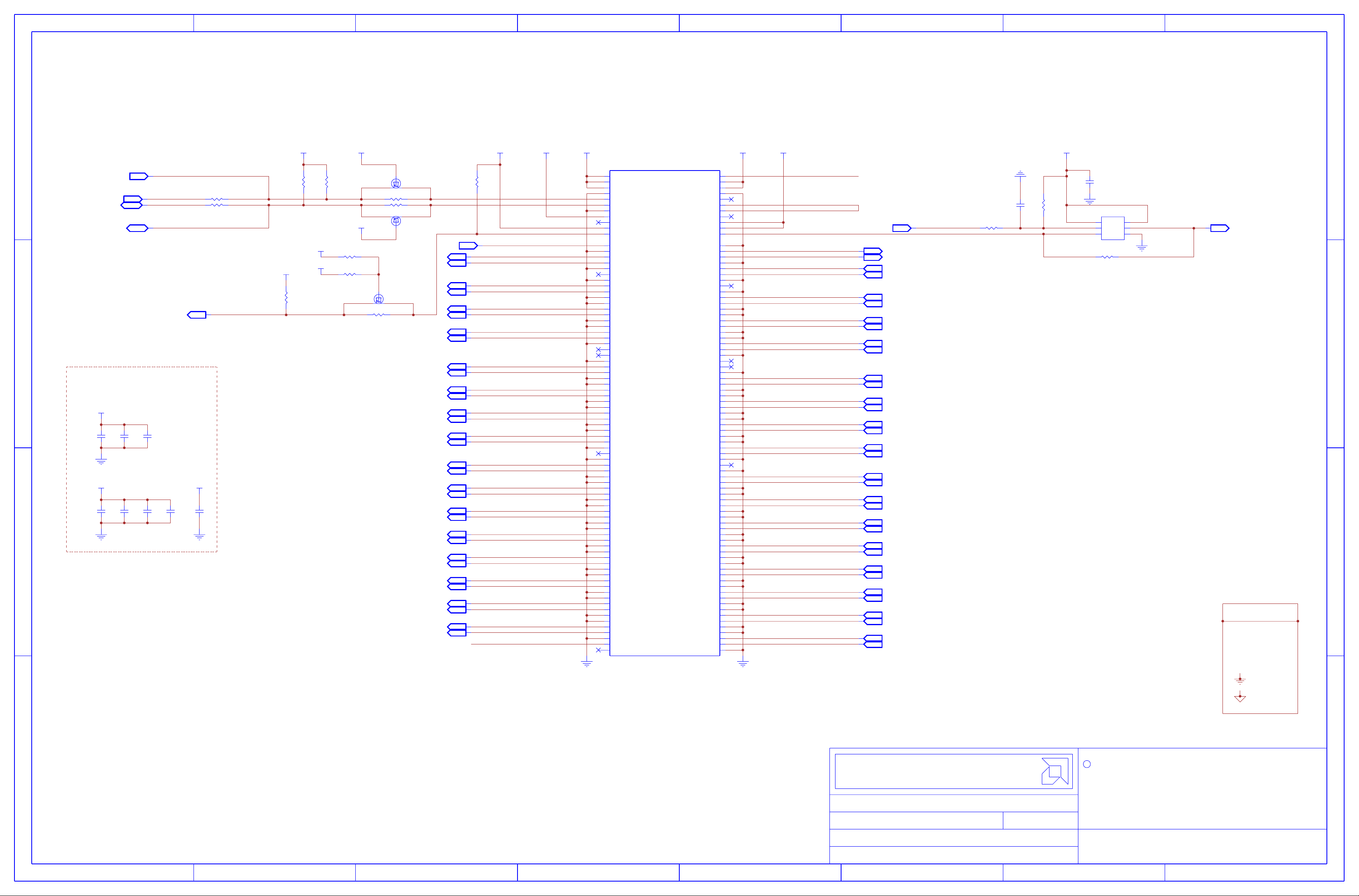
(1) PCI-EXPRESS EDGE CONNECTOR
(1) PCI-EXPRESS EDGE CONNECTOR
LMSMCLK
G_SMBCLK
G_SMBCLK
G_SMBDAT
G_SMBDAT
LMSMDATA
LMSMDATA
0.15uF
0.15uF
16V
16V
C155
C155
0.01uF
0.01uF
1uF
1uF
LMSMCLK
R113
R113
R112
R112
7
7
OUT
C156
C156
10V
10V
C165
C165
10uF
10uF
6.3V6.3V
6.3V6.3V
21
21
21
21
G_WAKEb
G_WAKEb
24
24
IN
8 24
8 24
24 8
24 8
PLACE THESE CAPS AS CLOSE TO
PLACE THESE CAPS AS CLOSE TO
PCIE CONNECTOR AS POSSIBLE
PCIE CONNECTOR AS POSSIBLE
+12V_BUS
+12V_BUS
+3.3V_BUS +3.3V_BUS
+3.3V_BUS +3.3V_BUS
IN
BI
24
24
BI
C157
C151 C152
C157
C151 C152
10uF
10uF
0.15uF
0.15uF
16V
16V
16V
16V
C153 C154
C153 C154
10uF 0.1uF
10uF 0.1uF
8
6.3V 6.3V
6.3V 6.3V
0R
5%
0R
5%
0R 5%
0R 5%
+3.3V_BUS
+3.3V_BUS
LIMITED TO OBFF
LIMITED TO OBFF
7
+3.3V_BUS
+3.3V_BUS
R107
R107
2.2K
2.2K
5%
5%
2 1
2 1
R103
45.3K
45.3K
1% 1%
1% 1%
2 1
2 1
+12V_BUS
+12V_BUS
+3.3V_BUS
+3.3V_BUS
+3.3V_BUS
+3.3V_BUS
1
1
Q100
R104
R104R103 R109
45.3K
45.3K
2 1
2 1
R110
R110
MR110
MR110
R105
R105
R106
R106
+3.3V_BUS
+3.3V_BUS
21
21
0R 5%
0R
21
21
R108
R108
5%0R
5%0R
5%
1
2
213
0R
0R
2
2
BSH111
BSH111
2
2
Q101
Q101
BSH111
BSH111
3
21
21
Q100
3
3
2 1
IN
2 1
1
1
5%
21
5%
21
21
21
3
3
Q110
Q110
BSH111
BSH111
1
1
5%
5%
0R
0R
5%
5%
0R
0R
7
7
2
2
OUT
2
2
OUT
2
2
OUT
2
2
OUT
2
2
OUT
2
2
OUT
2
2
OUT
2
2
OUT
2
2
OUT
2
2
OUT
2
2
OUT
2
2
OUT
2
2
OUT
2
2
OUT
2
2
OUT
2
2
OUT
2
2
OUT
2
2
OUT
2
2
OUT
2
2
OUT
2
2
OUT
2
2
OUT
2
2
OUT
2
2
OUT
2
2
OUT
2
2
OUT
2
2
OUT
2
2
OUT
2
2
OUT
2
2
OUT
2
2
OUT
2
2
OUT
6
+3.3V_AUX +3.3V_BUS
+3.3V_AUX +3.3V_BUS
R109
10K
10K
5%
5%
SMCLK
SMCLK
SMDAT
SMDAT
WAKEb
WAKEb
CLKREQb
CLKREQb
PETp0_GFXRp0
PETp0_GFXRp0
PETn0_GFXRn0
PETn0_GFXRn0
PETp1_GFXRp1
PETp1_GFXRp1
PETn1_GFXRn1
PETn1_GFXRn1
PETp2_GFXRp2
PETp2_GFXRp2
PETn2_GFXRn2
PETn2_GFXRn2
PETp3_GFXRp3
PETp3_GFXRp3
PETn3_GFXRn3
PETn3_GFXRn3
PETp4_GFXRp4
PETp4_GFXRp4
PETn4_GFXRn4
PETn4_GFXRn4
PETp5_GFXRp5
PETp5_GFXRp5
PETn5_GFXRn5
PETn5_GFXRn5
PETp6_GFXRp6
PETp6_GFXRp6
PETn6_GFXRn6
PETn6_GFXRn6
PETp7_GFXRp7
PETp7_GFXRp7
PETn7_GFXRn7
PETn7_GFXRn7
PETp8_GFXRp8
PETp8_GFXRp8
PETn8_GFXRn8
PETn8_GFXRn8
PETp9_GFXRp9
PETp9_GFXRp9
PETn9_GFXRn9
PETn9_GFXRn9
PETp10_GFXRp10
PETp10_GFXRp10
PETn10_GFXRn10
PETn10_GFXRn10
PETp11_GFXRp11
PETp11_GFXRp11
PETn11_GFXRn11
PETn11_GFXRn11
PETp12_GFXRp12
PETp12_GFXRp12
PETn12_GFXRn12
PETn12_GFXRn12
PETp13_GFXRp13
PETp13_GFXRp13
PETn13_GFXRn13
PETn13_GFXRn13
PETp14_GFXRp14
PETp14_GFXRp14
PETn14_GFXRn14
PETn14_GFXRn14
PETp15_GFXRp15
PETp15_GFXRp15
PETn15_GFXRn15
PETn15_GFXRn15
PRESENCE
PRESENCE
+12V_BUS
+12V_BUS
B10
B10
B11
B11
B12
B12
B13
B13
B14
B14
B15
B15
B16
B16
B17
B17
B18
B18
B19
B19
B20
B20
B21
B21
B22
B22
B23
B23
B24
B24
B25
B25
B26
B26
B27
B27
B28
B28
B29
B29
B30
B30
B31
B31
B32
B32
B33
B33
B34
B34
B35
B35
B36
B36
B37
B37
B38
B38
B39
B39
B40
B40
B41
B41
B42
B42
B43
B43
B44
B44
B45
B45
B46
B46
B47
B47
B48
B48
B49
B49
B50
B50
B51
B51
B52
B52
B53
B53
B54
B54
B55
B55
B56
B56
B57
B57
B58
B58
B59
B59
B60
B60
B61
B61
B62
B62
B63
B63
B64
B64
B65
B65
B66
B66
B67
B67
B68
B68
B69
B69
B70
B70
B71
B71
B72
B72
B73
B73
B74
B74
B75
B75
B76
B76
B77
B77
B78
B78
B79
B79
B80
B80
B81
B81
B82
B82
5
B1
B1
B2
B2
B3
B3
B4
B4
B5
B5
B6
B6
B7
B7
B8
B8
B9
B9
+12V
+12V
+12V
GND
SMCLK
SMDAT
GND
+3.3V
JTAG1
3.3Vaux
WAKE_
RSVD_B12
GND
PETp0
PETn0
GND
PRSNT2_B17
GND
PETp1
PETn1
GND
GND
PETp2
PETn2
GND
GND
PETp3
PETn3
GND
RSVD_B30
PRSNT2_B31
GND
PETp4
PETn4
GND
GND
PETp5
PETn5
GND
GND
PETp6
PETn6
GND
GND
PETp7
PETn7
GND
PRSNT2_B48
GND
PETp8
PETn8
GND
GND
PETp9
PETn9
GND
GND
PETp10
PETn10
GND
GND
PETp11
PETn11
GND
GND
PETp12
PETn12
GND
GND
PETp13
PETn13
GND
GND
PETp14
PETn14
GND
GND
PETp15
PETn15
GND
PRSNT2_B81
RSVD_B82
MPCIE1
MPCIE1
Mechanical Key
x16 PCIe
x16 PCIe
PRSNT1_A1
+12V
+12V
GND
JTAG2
JTAG3
JTAG4
JTAG5
+3.3V
+3.3V
PERST_
GND
REFCLK+
REFCLK-
GND
PERp0
PERn0
GND
RSVD_A19
GND
PERp1
PERn1
GND
GND
PERp2
PERn2
GND
GND
PERp3
PERn3
GND
RSVD_A32
RSVD_A33
GND
PERp4
PERn4
GND
GND
PERp5
PERn5
GND
GND
PERp6
PERn6
GND
GND
PERp7
PERn7
GND
RSVD_A50
GND
PERp8
PERn8
GND
GND
PERp9
PERn9
GND
GND
PERp10
PERn10
GND
GND
PERp11
PERn11
GND
GND
PERp12
PERn12
GND
GND
PERp13
PERn13
GND
GND
PERp14
PERn14
GND
GND
PERp15
PERn15
GND
+12V_BUS
+12V_BUS
A1
A1
A2
A2
A3
A3
A4
A4
A5
A5
A6
A6
A7
A7
A8
A8
A9
A9
A10
A10
A11
A11
A12
A12
A13
A13
A14
A14
A15
A15
A16
A16
A17
A17
A18
A18
A19
A19
A20
A20
A21
A21
A22
A22
A23
A23
A24
A24
A25
A25
A26
A26
A27
A27
A28
A28
A29
A29
A30
A30
A31
A31
A32
A32
A33
A33
A34
A34
A35
A35
A36
A36
A37
A37
A38
A38
A39
A39
A40
A40
A41
A41
A42
A42
A43
A43
A44
A44
A45
A45
A46
A46
A47
A47
A48
A48
A49
A49
A50
A50
A51
A51
A52
A52
A53
A53
A54
A54
A55
A55
A56
A56
A57
A57
A58
A58
A59
A59
A60
A60
A61
A61
A62
A62
A63
A63
A64
A64
A65
A65
A66
A66
A67
A67
A68
A68
A69
A69
A70
A70
A71
A71
A72
A72
A73
A73
A74
A74
A75
A75
A76
A76
A77
A77
A78
A78
A79
A79
A80
A80
A81
A81
A82
A82
DD
+3.3V_BUS
+3.3V_BUS
PRESENCE
PRESENCE
JTDIO_LOOP
JTDIO_LOOP
PCIE_REFCLKP
PCIE_REFCLKP
PCIE_REFCLKN
PCIE_REFCLKN
PERp0
PERp0
PERn0
PERn0
PERp1
PERp1
PERn1
PERn1
PERp2
PERp2
PERn2
PERn2
PERp3
PERp3
PERn3
PERn3
1
1
SYSTEM JTAG TDI AND
SYSTEM JTAG TDI AND
TDO ARE HARD WIRED.
TDO ARE HARD WIRED.
20 21
20 21
2
2
OUT
2
2
OUT
2
2
IN
2
2
IN
2
2
IN
2
2
IN
2
2
IN
2
2
IN
2
2
IN
2
2
IN
1.8V_EN
1.8V_EN
R102
R102
PERSTb
PERSTb
C159
C159
6.3V
6.3V
0R
0R
5%
21 4
21
5%
2 1
2 1
R111
R111
10K0.1uF
10K0.1uF
5%
5%
+3.3V_BUS
+3.3V_BUS
R120
R120
C158
C158
0.1uF
0.1uF
6.3V
6.3V
U100
U100
3
3
A
1
1
B
C
74AUP1G57GM
74AUP1G57GM
DNI
DNI
VCC
GND
5
5
4
Y
26
26
5%
5%
21
21
1K
1K
PERSTb_BUF
PERSTb_BUF
23 21 2
OUTIN
23 21 2
C
PERp4
PERp4
PERn4
PERn4
PERp5
PERp5
PERn5
PERn5
PERp6
PERp6
PERn6
PERn6
PERp7
PERp7
PERn7
PERn7
PERp8
PERp8
PERn8
PERn8
PERp9
PERp9
PERn9
PERn9
PERp10
PERp10
PERn10
PERn10
PERp11
PERp11
PERn11
PERn11
PERp12
PERp12
PERn12
PERn12
PERp13
PERp13
PERn13
PERn13
PERp14
PERp14
PERn14
PERn14
PERp15
PERp15
PERn15
PERn15
AMD - PLATFORM HARDWARE ENG
AMD - PLATFORM HARDWARE ENG
#48, No.1387, ZHANGDONG ROAD
#48, No.1387, ZHANGDONG ROAD
SHANGHAI, CHINA 201203
SHANGHAI, CHINA 201203
SHEET:
DATE:
SHEET NUMBER:
DOCUMENT NUMBER:
4
2
2
IN
2
2
IN
2
2
IN
2
2
IN
2
2
IN
2
2
IN
2
2
IN
2
2
IN
2
2
IN
2
2
IN
2
2
IN
2
2
IN
2
2
IN
2
2
IN
2
2
IN
2
2
IN
2
2
IN
2
2
IN
2
2
IN
2
2
IN
2
2
IN
2
2
IN
2
2
IN
2
2
IN
PCIE EDGE CONNECTOR
PCIE EDGE CONNECTOR
Wed Apr 13 17:02:06 2016 1.0
Wed Apr 13 17:02:06 2016 1.0
1 26
1 26
OF
105_D009XX_00
105_D009XX_00
REV:
3
SYMBOL LEGEND
SYMBOL LEGEND
DNI
DNI
b or #
b or #
BUO
BUO
CONFIDENTIAL AND PROPRIETARY TO ADVANCED MICRO DEVICES INC.
2016
2016
C
This AMD Board schematic and design is the exclusive property of AMD, and
is provided only to entities under a non-disclosure agreement with AMD
for evaluation purposes. Further distribution or disclosure is strictly
prohibited. Use of this schematic and design for any purpose other than
evaluation requires a Board Technology License Agreement with AMD.
AMD makes no representations or warranties of any kind regarding this
schematic and design, including, not limited to, any implied warranty
of merchantability or fitness for a particular purpose, and disclaims
responsibility for any consequences resulting from use of the
information included herein.
TITLE:
2
Advanced Micro Devices
Ellesmere XT/PRO GD5 8L
Ellesmere XT/PRO GD5 8L
1
DO NOT
DO NOT
INSTALL
INSTALL
ACTIVE
ACTIVE
LOW
LOW
BRING UP
BRING UP
ONLY
ONLY
DIGITAL
DIGITAL
GROUND
GROUND
ANALOG
ANALOG
GROUND
GROUND
BB
A
Page 2
This AMD Board schematic and design is the exclusive property of AMD, and
DATE:
SHEET:
Advanced Micro Devices
2
3
345
6
6
7
7
8
8
C
5
CONFIDENTIAL AND PROPRIETARY TO ADVANCED MICRO DEVICES INC.
C
BB
A
1
DD
C
A
4
REV:
SHEET NUMBER:
DOCUMENT NUMBER:
OF
1
prohibited. Use of this schematic and design for any purpose other than
for evaluation purposes. Further distribution or disclosure is strictly
is provided only to entities under a non-disclosure agreement with AMD
2
schematic and design, including, not limited to, any implied warranty
AMD makes no representations or warranties of any kind regarding this
evaluation requires a Board Technology License Agreement with AMD.
of merchantability or fitness for a particular purpose, and disclaims
responsibility for any consequences resulting from use of the
information included herein.
TITLE:
INININININININININININININ
REV 0.90
S
S
E
R
P
X
E
I
C
P
PART 2 OF 18
VSS
VSS
VDD_08
VDD_18
VDD_18
VDD_18
VDD_18
VDD_18
VDD_18
VDD_08
VDD_08
VDD_08
VDD_08
VDD_08
VDD_08
VDD_08
VDD_08
VDD_08
VDD_08
PCIE_ZVSS
PX_EN
PCIE_RX15N
PCIE_RX15P
PCIE_RX14N
PCIE_RX14P
PCIE_RX13N
PCIE_RX13P
PCIE_RX12N
PCIE_RX12P
PCIE_RX11N
PCIE_RX11P
PCIE_RX10N
PCIE_RX10P
PCIE_RX9N
PCIE_RX9P
PCIE_RX8N
PCIE_RX8P
PCIE_RX7N
PCIE_RX7P
PCIE_RX6N
PCIE_RX6P
PCIE_RX5N
PCIE_RX5P
PCIE_RX4N
PCIE_RX4P
PCIE_RX3N
PCIE_RX3P
PCIE_RX2N
PCIE_RX2P
PCIE_RX1N
PCIE_RX1P
PCIE_RX0N
PCIE_RX0P
PCIE_REFCLKN
PCIE_REFCLKP
PERSTB
PCIE_TX15N
PCIE_TX15P
PCIE_TX14N
PCIE_TX14P
PCIE_TX13N
PCIE_TX13P
PCIE_TX12N
PCIE_TX12P
PCIE_TX11N
PCIE_TX11P
PCIE_TX10N
PCIE_TX10P
PCIE_TX9N
PCIE_TX9P
PCIE_TX8N
PCIE_TX8P
PCIE_TX7N
PCIE_TX7P
PCIE_TX6N
PCIE_TX6P
PCIE_TX5N
PCIE_TX5P
PCIE_TX4N
PCIE_TX4P
PCIE_TX3N
PCIE_TX3P
PCIE_TX2N
PCIE_TX2P
PCIE_TX1N
PCIE_TX1P
PCIE_TX0N
PCIE_TX0P
OUT
OUT
OUT
OUT
OUT
OUT
OUT
OUT
OUT
OUT
OUT
OUT
OUT
OUT
OUT
OUT
OUT
OUT
OUT
OUT
OUT
OUT
OUT
OUT
OUT
OUT
OUT
OUT
OUT
OUT
OUT
OUT
OUTININININININININININININININININININININININ
IN
8
7
6
345
2
1
C
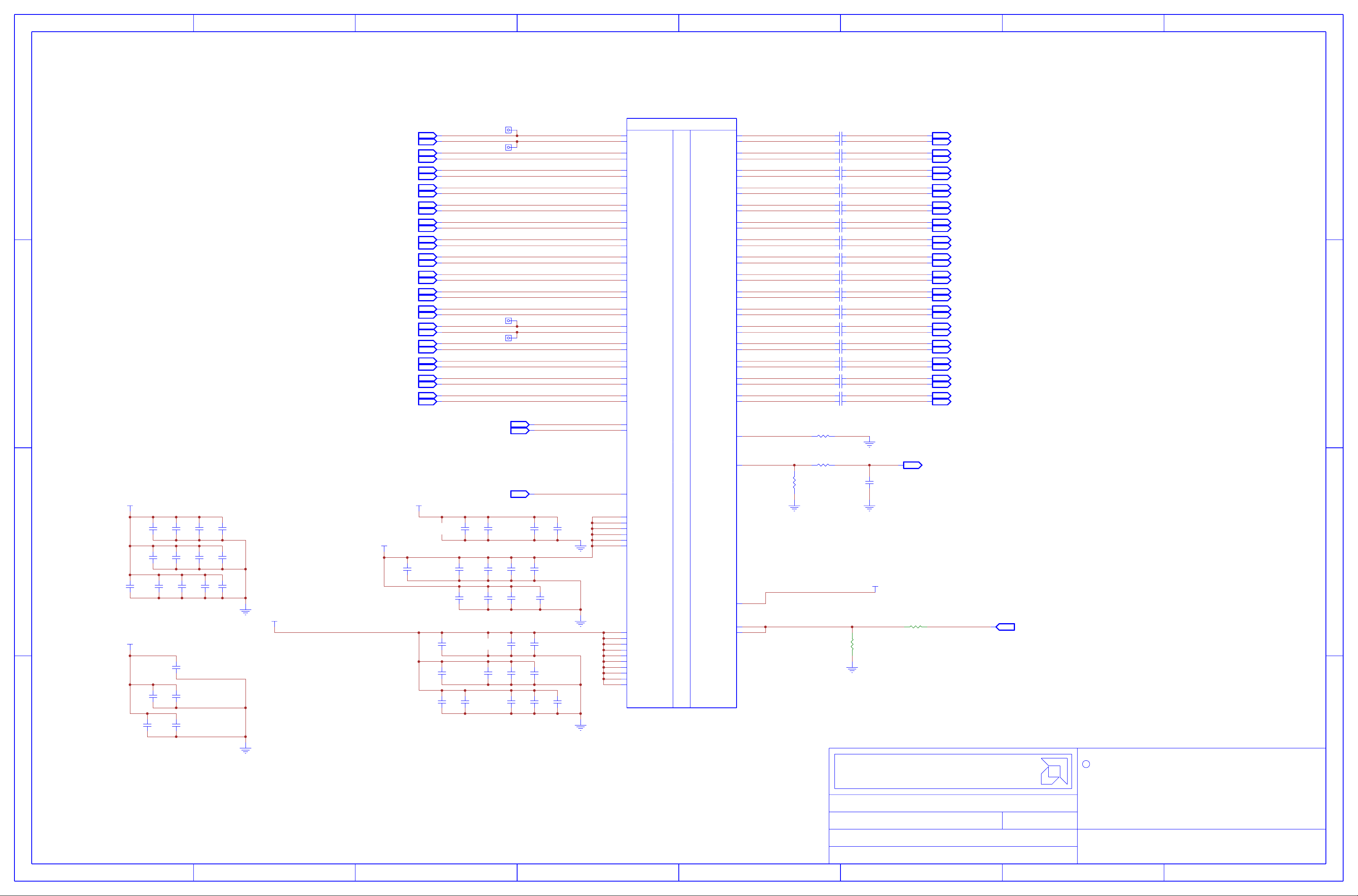
(2) ELLESMERE PCIE INTERFACE
(2) ELLESMERE PCIE INTERFACE
+1.8V
+1.8V
+0.8V
+0.8V
1uF 1uF
1uF 1uF
6.3V
6.3V
C1703
C1703
6.3V
6.3V
C1706
C1706
6.3V
6.3V
2 1
2 1
OVERLAP
OVERLAP
1uF
1uF
6.3V
6.3V
C1704
C1704
6.3V 6.3V
6.3V 6.3V
MC1707
MC1707
C1707
C1707
4.7uF
22uF4.7uF
4.7uF
22uF4.7uF
6.3V4V
6.3V4V
6.3V
6.3V
C1705
C1705
0.1uF0.1uF0.1uF
0.1uF0.1uF0.1uF
6.3V
6.3V
C1708
C1708
4.7uF
4.7uF
6.3V
6.3V
C1738C1702C1701C1700
C1738C1702C1701C1700
1uF
1uF
C1719
C1719
0.1uF
0.1uF
C1709
C1709
4.7uF
4.7uF
6.3V
6.3V
+0.8V
+0.8V
C1711
C1711
1uF
1uF
6.3V
6.3V
C1714C1713
C1714C1713
0.1uF
0.1uF
0.1uF
0.1uF
6.3V
6.3V
6.3V
6.3V
MC1717
MC1717
22uF
22uF
4V
4V
2 1
2 1
OVERLAP
OVERLAP
C1717
C1717
4.7uF
4.7uF
6.3V
6.3V
+1.8V
+1.8V
1
1
1
1
1
1
1
1
1
1
1
1
1
1
1
1
1
1
1
1
1
1
1
1
1
1
1
1
1
1
1
1
1
1
1
1
1
1
1
1
1
1
1
1
1
1
1
1
1
1
1
1
1
1
1
1
1
1
1
1
1
1
1
1
+0.8V
+0.8V
MC141
MC141
10uF
10uF
6.3V
6.3V
IN
IN
IN
IN
IN
IN
IN
IN
IN
IN
IN
IN
IN
IN
IN
IN
IN
IN
IN
IN
IN
IN
IN
IN
IN
IN
IN
IN
IN
IN
IN
IN
OVERLAP
OVERLAP
C133
C133
1uF
1uF
6.3V
6.3V
C147
C147
1uF
1uF
6.3V
6.3V
0.1uF
0.1uF
6.3V
6.3V
TP101
TP101
TP102
TP102
TP117
TP117
TP118
TP118
1uF
1uF
6.3V 6.3V
6.3V 6.3V
4.7uF
4.7uF
6.3V
6.3V
C137
C137
1uF
1uF
6.3V
6.3V
C162C161
C162C161
0.1uF
0.1uF
6.3V
6.3V
PETp0_GFXRp0
PETp0_GFXRp0
PETn0_GFXRn0
PETn0_GFXRn0
PETp1_GFXRp1
PETp1_GFXRp1
PETn1_GFXRn1
PETn1_GFXRn1
PETp2_GFXRp2
PETp2_GFXRp2
PETn2_GFXRn2
PETn2_GFXRn2
PETp3_GFXRp3
PETp3_GFXRp3
PETn3_GFXRn3
PETn3_GFXRn3
PETp4_GFXRp4
PETp4_GFXRp4
PETn4_GFXRn4
PETn4_GFXRn4
PETp5_GFXRp5
PETp5_GFXRp5
PETn5_GFXRn5
PETn5_GFXRn5
PETp6_GFXRp6
PETp6_GFXRp6
PETn6_GFXRn6
PETn6_GFXRn6
PETp7_GFXRp7
PETp7_GFXRp7
PETn7_GFXRn7
PETn7_GFXRn7
PETp8_GFXRp8
PETp8_GFXRp8
PETn8_GFXRn8
PETn8_GFXRn8
PETp9_GFXRp9
PETp9_GFXRp9
PETn9_GFXRn9
PETn9_GFXRn9
PETp10_GFXRp10
PETp10_GFXRp10
PETn10_GFXRn10
PETn10_GFXRn10
PETp11_GFXRp11
PETp11_GFXRp11
PETn11_GFXRn11
PETn11_GFXRn11
PETp12_GFXRp12
PETp12_GFXRp12
PETn12_GFXRn12
PETn12_GFXRn12
PETp13_GFXRp13
PETp13_GFXRp13
PETn13_GFXRn13
PETn13_GFXRn13
PETp14_GFXRp14
PETp14_GFXRp14
PETn14_GFXRn14
PETn14_GFXRn14
PETp15_GFXRp15
PETp15_GFXRp15
PETn15_GFXRn15
PETn15_GFXRn15
PCIE_REFCLKP
C139
C139
0.1uF
0.1uF
6.3V
6.3V
C142
C142
6.3V
6.3V
C145
C145
1uF
1uF
6.3V
6.3V
1uF
1uF
6.3V
6.3V
10u
10u
C160
C160
10uF
10uF
4V
4V
PCIE_REFCLKP
PCIE_REFCLKN
PCIE_REFCLKN
PERSTb_BUF
PERSTb_BUF
C172
C172
1uF
1uF
6.3V
6.3V
C140
C140
0.01uF
0.01uF
6.3V
6.3V
C30
C30
1uF1uF
1uF1uF
6.3V
6.3V
C146
C146
1uF
1uF
6.3V
6.3V
C1319
C1319
1uF
1uF
6.3V
6.3V
C148
C148
4.7uF
4.7uF
6.3V
6.3V
2 1
2 1
1uF
1uF
6.3V6.3V
6.3V6.3V
MC148
MC148
22uF
22uF
4V
4V
1
1
IN
1
1
IN
1 21 23
1 21 23
IN
C177C176 C173
C177C176 C173
1uF
1uF
C136C141
C136C141
1uF
1uF
6.3V
6.3V
C138
C138
1uF
1uF
6.3V
6.3V
C1284
C150
C150
C1284
1uF
1uF
6.3V
6.3V
2 1
2 1
AN42
AN42
AN43
AN43
AN41
AN41
AM41
AM41
AM43
AM43
AM42
AM42
AK43
AK43
AK42
AK42
AJ42
AJ42
AJ43
AJ43
AJ41
AJ41
AG41
AG41
AG43
AG43
AG42
AG42
AF43
AF43
AF42
AF42
AE42
AE42
AE43
AE43
AE41
AE41
AD41
AD41
AD43
AD43
AD42
AD42
AC43
AC43
AC42
AC42
AA42
AA42
AA43
AA43
AA41
AA41
Y41
Y41
Y43
Y43
Y42
Y42
W42
W42
W43
W43
AR42
AR42
AR43
AR43
AV42
AV42
AM25
AM25
AN25
AN25
AN26
AN26
AP26
AP26
AP27
AP27
AR27
AR27
AA34
AA34
AA35
AA35
AD36
AD36
AE35
AE35
AF35
AF35
AG36
AG36
AJ35
AJ35
AK35
AK35
AM36
AM36
AN35
AN35
PCIE_RX0P
PCIE_RX0N
PCIE_RX1P
PCIE_RX1N
PCIE_RX2P
PCIE_RX2N
PCIE_RX3P
PCIE_RX3N
PCIE_RX4P
PCIE_RX4N
PCIE_RX5P
PCIE_RX5N
PCIE_RX6P
PCIE_RX6N
PCIE_RX7P
PCIE_RX7N
PCIE_RX8P
PCIE_RX8N
PCIE_RX9P
PCIE_RX9N
PCIE_RX10P
PCIE_RX10N
PCIE_RX11P
PCIE_RX11N
PCIE_RX12P
PCIE_RX12N
PCIE_RX13P
PCIE_RX13N
PCIE_RX14P
PCIE_RX14N
PCIE_RX15P
PCIE_RX15N
PCIE_REFCLKP
PCIE_REFCLKN
PERSTB
VDD_18
VDD_18
VDD_18
VDD_18
VDD_18
VDD_18
VDD_08
VDD_08
VDD_08
VDD_08
VDD_08
VDD_08
VDD_08
VDD_08
VDD_08
VDD_08
U1
U1
PART 2 OF 18
P
C
I
E
X
P
R
E
S
S
ellesmere_l4
ellesmere_l4
PCIE_TX0P
PCIE_TX0N
PCIE_TX1P
PCIE_TX1N
PCIE_TX2P
PCIE_TX2N
PCIE_TX3P
PCIE_TX3N
PCIE_TX4P
PCIE_TX4N
PCIE_TX5P
PCIE_TX5N
PCIE_TX6P
PCIE_TX6N
PCIE_TX7P
PCIE_TX7N
PCIE_TX8P
PCIE_TX8N
PCIE_TX9P
PCIE_TX9N
PCIE_TX10P
PCIE_TX10N
PCIE_TX11P
PCIE_TX11N
PCIE_TX12P
PCIE_TX12N
PCIE_TX13P
PCIE_TX13N
PCIE_TX14P
PCIE_TX14N
PCIE_TX15P
PCIE_TX15N
PCIE_ZVSS
PX_EN
VDD_08
VSS
VSS
REV 0.90
AR38
AR38
AR39
AR39
AR37
AR37
AN37
AN37
AN39
AN39
AN38
AN38
AM39
AM39
AM38
AM38
AK38
AK38
AK39
AK39
AK37
AK37
AJ37
AJ37
AJ39
AJ39
AJ38
AJ38
AG39
AG39
AG38
AG38
AF38
AF38
AF39
AF39
AF37
AF37
AE37
AE37
AE39
AE39
AE38
AE38
AD39
AD39
AD38
AD38
AC38
AC38
AC39
AC39
AC37
AC37
AA37
AA37
AA39
AA39
AA38
AA38
Y38
Y38
Y39
Y39
AK30
AK30
V40
V40
AJ30
AJ30
AJ29
AJ29
AK29
AK29
PCIE_TX0P
PCIE_TX0P
PCIE_TX0N
PCIE_TX0N
PCIE_TX1P
PCIE_TX1P
PCIE_TX1N
PCIE_TX1N
PCIE_TX2P
PCIE_TX2P
PCIE_TX2N
PCIE_TX2N
PCIE_TX3P
PCIE_TX3P
PCIE_TX3N
PCIE_TX3N
PCIE_TX4P
PCIE_TX4P
PCIE_TX4N
PCIE_TX4N
PCIE_TX5P
PCIE_TX5P
PCIE_TX5N
PCIE_TX5N
PCIE_TX6P
PCIE_TX6P
PCIE_TX6N
PCIE_TX6N
PCIE_TX7P
PCIE_TX7P
PCIE_TX7N
PCIE_TX7N
PCIE_TX8P
PCIE_TX8P
PCIE_TX8N
PCIE_TX8N
PCIE_TX9P
PCIE_TX9P
PCIE_TX9N
PCIE_TX9N
PCIE_TX10P
PCIE_TX10P
PCIE_TX10N
PCIE_TX10N
PCIE_TX11P
PCIE_TX11P
PCIE_TX11N
PCIE_TX11N
PCIE_TX12P
PCIE_TX12P
PCIE_TX12N
PCIE_TX12N
PCIE_TX13P
PCIE_TX13P
PCIE_TX13N
PCIE_TX13N
PCIE_TX14P
PCIE_TX14P
PCIE_TX14N
PCIE_TX14N
PCIE_TX15P
PCIE_TX15P
PCIE_TX15N
PCIE_TX15N
PCIE_ZVSS
PCIE_ZVSS
R155
R156
R150
R150
DNI
DNI
PERp0
PX_EN
PX_EN
0.1uF
0.1uF
PERp0
PERn0
PERn0
PERp1
PERp1
PERn1
PERn1
PERp2
PERp2
PERn2
PERn2
PERp3
PERp3
PERn3
PERn3
PERp4
PERp4
PERn4
PERn4
PERp5
PERp5
PERn5
PERn5
PERp6
PERp6
PERn6
PERn6
PERp7
PERp7
PERn7
PERn7
PERp8
PERp8
PERn8
PERn8
PERp9
PERp9
PERn9
PERn9
PERp10
PERp10
PERn10
PERn10
PERp11
PERp11
PERn11
PERn11
PERp12
PERp12
PERn12
PERn12
PERp13
PERp13
PERn13
PERn13
PERp14
PERp14
PERn14
PERn14
PERp15
PERp15
PERn15
PERn15
OUT
OUT
OUT
OUT
OUT
OUT
OUT
OUT
OUT
OUT
OUT
OUT
OUT
OUT
OUT
OUT
OUT
OUT
OUT
OUT
OUT
OUT
OUT
OUT
OUT
OUT
OUT
OUT
OUT
OUT
OUT
OUT
OUT
21 24
21 24 23
23
1
1
1
1
1
1
1
1
1
1
1
1
1
1
1
1
1
1
1
1
1
1
1
1
1
1
1
1
1
1
1
1
1
1
1
1
1
1
1
1
1
1
1
1
1
1
1
1
1
1
1
1
1
1
1
1
1
1
1
1
1
1
1
1
C100
C100
C101
C101
C102
C102
C103
C103
C104
C104
C105
C105
C106
C106
C107
C107
C108
C108
C109
C109
C111
C111
C110
C110
C112
C112
C113
C113
C114
C114
C115
C115
C116
C116
C117
C117
C118
C118
C119
C119
C120
C120
C121
C121
C122
C122
C123
C123
C124
C124
C125
C125
C126
C126
C127
C127
C128
C128
C129
C129
C130
C130
C131
C131
21
21R155
21R156
21
0R 5%
0R 5%
1K
1K
5%
5%
6.3V0.22uF
6.3V0.22uF
6.3V0.22uF
6.3V0.22uF
6.3V0.22uF
6.3V0.22uF
6.3V0.22uF
6.3V0.22uF
0.22uF
6.3V
6.3V
0.22uF
0.22uF
6.3V
0.22uF
6.3V
6.3V
0.22uF
6.3V
0.22uF
6.3V0.22uF
6.3V0.22uF
6.3V0.22uF
6.3V0.22uF
0.22uF
0.22uF
6.3V
6.3V
6.3V
6.3V
0.22uF
0.22uF
0.22uF
6.3V
6.3V
0.22uF
0.22uF
0.22uF
6.3V
6.3V
6.3V0.22uF
6.3V0.22uF
0.22uF 6.3V
0.22uF 6.3V
6.3V0.22uF
6.3V0.22uF
6.3V0.22uF
6.3V0.22uF
6.3V0.22uF
6.3V0.22uF
6.3V
0.22uF
6.3V
0.22uF
0.22uF
6.3V
6.3V
0.22uF
6.3V
6.3V
0.22uF
0.22uF
6.3V
6.3V
0.22uF
0.22uF
6.3V
0.22uF
0.22uF
6.3V
6.3V0.22uF
6.3V0.22uF
0.22uF 6.3V
0.22uF 6.3V
6.3V0.22uF
6.3V0.22uF
0.22uF 6.3V
0.22uF 6.3V
6.3V0.22uF
6.3V0.22uF
6.3V0.22uF
6.3V0.22uF
0.22uF 6.3V
0.22uF 6.3V
0.22uF 6.3V
0.22uF 6.3V
0.22uF 6.3V
0.22uF 6.3V
1%200R
1%200R
C258
C258
6.3V
6.3V
2 1
2 1
DD
C
BB
+0.8V
+0.8V
EVDDQ_G
EVDDQ_G
R4302
R4302
1K
1K
5%
5%
2 1
2 1
R4301
R4301
0R
0R
21
21
EVDDQ5%
5%
EVDDQ
IN
24
24
Check BOM for more detail
A
7
8
Check BOM for more detail
6
AMD - PLATFORM HARDWARE ENG
AMD - PLATFORM HARDWARE ENG
#48, No.1387, ZHANGDONG ROAD
#48, No.1387, ZHANGDONG ROAD
SHANGHAI, CHINA 201203
SHANGHAI, CHINA 201203
SHEET:
DATE:
SHEET NUMBER:
DOCUMENT NUMBER:
5
4
ELLESMERE PCIE INTERFACE
ELLESMERE PCIE INTERFACE
Wed Apr 13 17:02:07 2016 1.0
Wed Apr 13 17:02:07 2016 1.0
2 26
2 26
OF
105_D009XX_00
105_D009XX_00
REV:
3
CONFIDENTIAL AND PROPRIETARY TO ADVANCED MICRO DEVICES INC.
2016
2016
C
This AMD Board schematic and design is the exclusive property of AMD, and
is provided only to entities under a non-disclosure agreement with AMD
for evaluation purposes. Further distribution or disclosure is strictly
prohibited. Use of this schematic and design for any purpose other than
evaluation requires a Board Technology License Agreement with AMD.
AMD makes no representations or warranties of any kind regarding this
schematic and design, including, not limited to, any implied warranty
of merchantability or fitness for a particular purpose, and disclaims
responsibility for any consequences resulting from use of the
information included herein.
TITLE:
2
Advanced Micro Devices
Ellesmere XT/PRO GD5 8L
Ellesmere XT/PRO GD5 8L
1
A
Page 3
This AMD Board schematic and design is the exclusive property of AMD, and
DATE:
SHEET:
Advanced Micro Devices
2
3
345
6
6
7
7
8
8
C
5
CONFIDENTIAL AND PROPRIETARY TO ADVANCED MICRO DEVICES INC.
C
BB
A
1
DD
C
A
4
REV:
SHEET NUMBER:
DOCUMENT NUMBER:
OF
1
prohibited. Use of this schematic and design for any purpose other than
for evaluation purposes. Further distribution or disclosure is strictly
is provided only to entities under a non-disclosure agreement with AMD
2
schematic and design, including, not limited to, any implied warranty
AMD makes no representations or warranties of any kind regarding this
evaluation requires a Board Technology License Agreement with AMD.
of merchantability or fitness for a particular purpose, and disclaims
responsibility for any consequences resulting from use of the
information included herein.
TITLE:
OUT
OUT
OUT
OUTBIBIBIBI
OUT
REV 0.90
B
K
N
A
B
E
C
A
F
R
E
T
N
I
Y
R
O
M
E
M
PART 4 OF 18
DRAM_RSTB
MEM_CALRB
MAB1_9MAB0_9
CLKB1B
CLKB1
CKEB1
WCKB1B_1
WCKB1_1
WCKB1B_0
WCKB1_0
ADBIB1
RASB1B
CASB1B
CSB1B_0
WEB1B
DDBIB1_3
DDBIB1_2
DDBIB1_1
DDBIB1_0
EDCB1_3
EDCB1_2
EDCB1_1
EDCB1_0
MVREFDB
CLKB0B
CLKB0
CKEB0
RASB0B
CASB0B
CSB0B_0
WEB0B
DDBIB0_3
DDBIB0_2
DDBIB0_1
DDBIB0_0
EDCB0_3
EDCB0_2
EDCB0_1
EDCB0_0
WCKB0B_1
WCKB0_1
WCKB0B_0
WCKB0_0
ADBIB0
MAB0_8
MAB0_7
MAB0_6
MAB0_5
MAB0_4
MAB0_3
MAB0_2
MAB0_1
MAB0_0
MAB1_8
MAB1_7
MAB1_6
MAB1_5
MAB1_4
MAB1_3
MAB1_2
MAB1_1
MAB1_0
DQB1_31
DQB1_30
DQB1_29
DQB1_28
DQB1_27
DQB1_26
DQB1_25
DQB1_24
DQB1_23
DQB1_22
DQB1_21
DQB1_20
DQB1_19
DQB1_18
DQB1_17
DQB1_16
DQB1_15
DQB1_14
DQB1_13
DQB1_12
DQB1_11
DQB1_10
DQB1_9
DQB1_8
DQB1_7
DQB1_6
DQB1_5
DQB1_4
DQB1_3
DQB1_2
DQB1_1
DQB1_0
DQB0_31
DQB0_30
DQB0_29
DQB0_28
DQB0_27
DQB0_26
DQB0_25
DQB0_24
DQB0_23
DQB0_22
DQB0_21
DQB0_20
DQB0_19
DQB0_18
DQB0_17
DQB0_16
DQB0_15
DQB0_14
DQB0_13
DQB0_12
DQB0_11
DQB0_10
DQB0_9
DQB0_8
DQB0_7
DQB0_6
DQB0_5
DQB0_4
DQB0_3
DQB0_2
DQB0_1
DQB0_0
REV 0.90
PART 3 OF 18
A
K
N
A
B
E
C
A
F
R
E
T
N
I
Y
R
O
M
E
M
DRAM_RSTA
MEM_CALRA
MAA1_9MAA0_9
CLKA0B
CLKA0
CLKA1B
CLKA1
CKEA1
RASA1B
CASA1B
CSA1B_0
WEA1B
DDBIA1_3
DDBIA1_2
DDBIA1_1
DDBIA1_0
EDCA1_3
EDCA1_2
EDCA1_1
EDCA1_0
WCKA1B_1
WCKA1_1
WCKA1B_0
WCKA1_0
MVREFDA
CKEA0
RASA0B
CASA0B
CSA0B_0
WEA0B
DDBIA0_3
DDBIA0_2
DDBIA0_1
DDBIA0_0
EDCA0_3
EDCA0_2
EDCA0_1
EDCA0_0
WCKA0B_1
WCKA0_1
WCKA0B_0
WCKA0_0
ADBIA0 ADBIA1
MAA1_8
MAA1_7
MAA1_6
MAA1_5
MAA1_4
MAA1_3
MAA1_2
MAA1_1
MAA1_0
DQA1_31
DQA1_30
DQA1_29
DQA1_28
DQA1_27
DQA1_26
DQA1_25
DQA1_24
DQA1_23
DQA1_22
DQA1_21
DQA1_20
DQA1_19
DQA1_18
DQA1_17
DQA1_16
DQA1_15
DQA1_14
DQA1_13
DQA1_12
DQA1_11
DQA1_10
DQA1_9
DQA1_8
DQA1_7
DQA1_6
DQA1_5
DQA1_4
DQA1_3
DQA1_2
DQA1_1
DQA1_0
MAA0_8
MAA0_7
MAA0_6
MAA0_5
MAA0_4
MAA0_3
MAA0_2
MAA0_1
MAA0_0
DQA0_31
DQA0_30
DQA0_29
DQA0_28
DQA0_27
DQA0_26
DQA0_25
DQA0_24
DQA0_23
DQA0_22
DQA0_21
DQA0_20
DQA0_19
DQA0_18
DQA0_17
DQA0_16
DQA0_15
DQA0_14
DQA0_13
DQA0_12
DQA0_11
DQA0_10
DQA0_9
DQA0_8
DQA0_7
DQA0_6
DQA0_5
DQA0_4
DQA0_3
DQA0_2
DQA0_1
DQA0_0
OUT
OUT
OUT
OUT
OUT
OUT
OUT
OUTBIBIBIBIBIBIBIBIBIBIBIBIBIOUT
OUT
OUT
OUT
OUT
OUT
OUTBIBIBIBIBIBIBIBIBIBIBIBI
BI
OUT
OUT
OUT
OUT
OUT
OUT
OUTBIBIBIBIBIBIBIBIBIBIBIBIBIOUT
OUT
OUT
OUT
OUT
OUT
OUTBIBIBIBIBIBIBIBIBIBIBIBI
BI
8
7
6
345
2
1
C
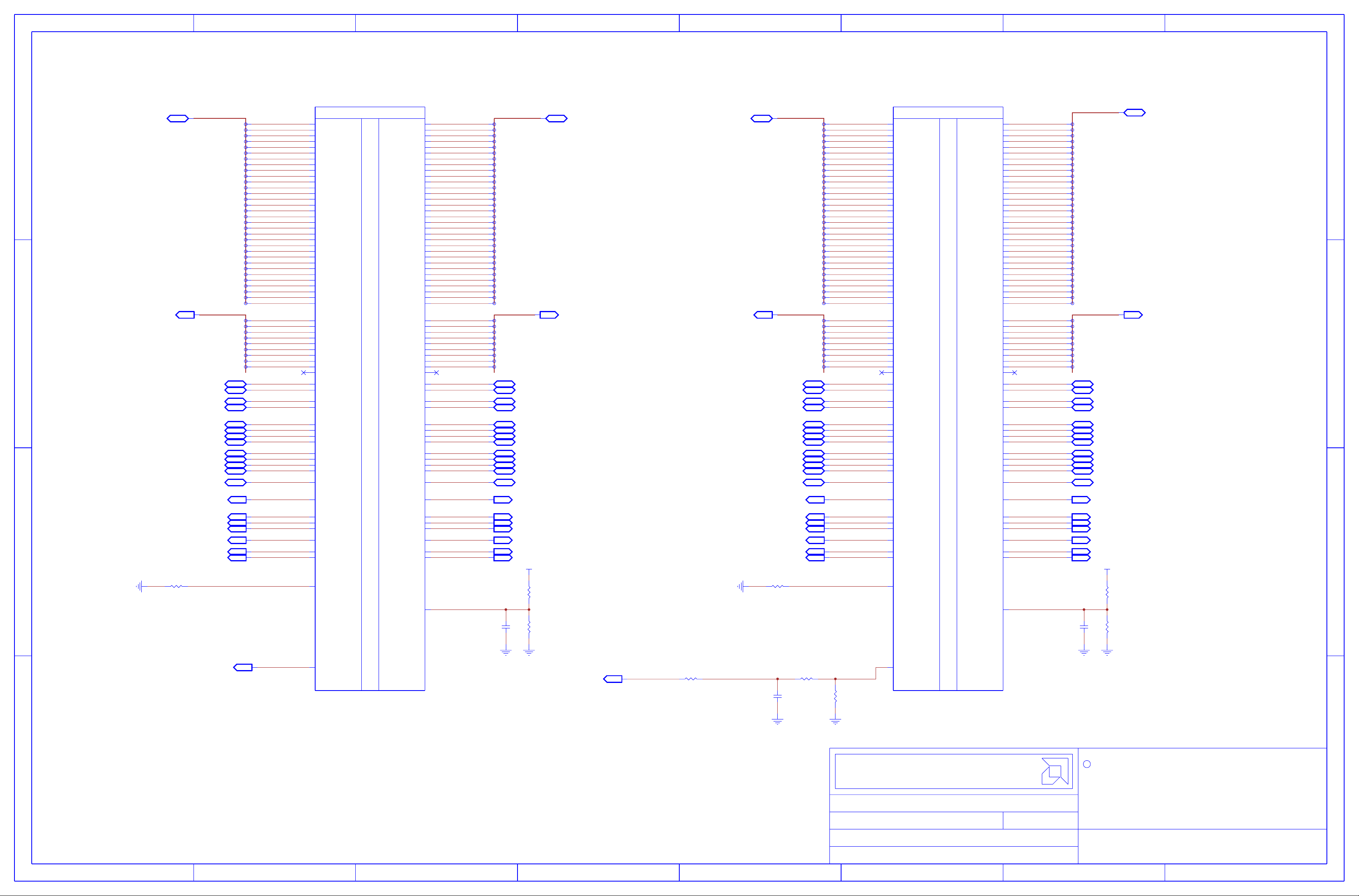
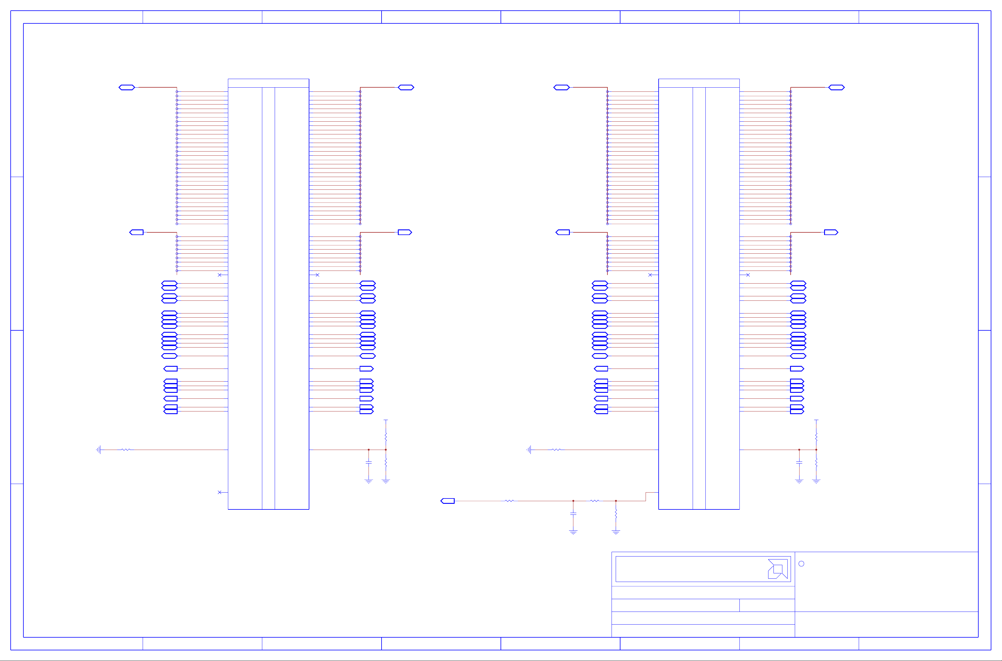
(3) ELLESMERE MEM INTERFACE CH A/B
(3) ELLESMERE MEM INTERFACE CH A/B
3 5
3 5
3 5
3 5
3 5
3 5
3 5
3 5
3 5
3 5
3 5
3 5
3 5
3 5
3 5
3 5
3 5
3 5
3 5
3 5
3 5
3 5
3 5
3 5
3 5
3 5
3 5
3 5
3 5
3 5
3 5
3 5
3 5
3 5
3 5
3 5
3 5
3 5
3 5
3 5
3 5
3 5
3 5
3 5
3 5
3 5
3 5
3 5
3 5
3 5
3 5
3 5
3 5
3 5
3 5
3 5
3 5
3 5
3 5
3 5
3 5
3 5
MAA0_<9..0> MAB1_<9..0>
5 3 5 3
5 3 5 3
2 1
2 1
120R
120R
MAA0_<9..0> MAB1_<9..0>
OUT OUT OUTOUT
3 5
3 5
3 5
3 5
3 5
3 5
3 5
3 5
3 5
3 5
3 5
3 5
3 5
3 5
3 5
3 5
5
5
BI
5
5
BI
5
5
BI
5
5
BI
5
5
BI
5
5
BI
5
5
BI
5
5
BI
5
5
BI
5
5
BI
5
5
BI
5
5
BI
5 5
5 5
BI
5
5
OUT
5
5
OUT
5
5
OUT
5
5
OUT
5
5
OUT
5
5
OUT
5 5
5 5
OUT
1%
1%
R3610
R3610
MEM_CALRA
MEM_CALRA
U1
U1
5
5
3
DQA0_<0>
3
DQA0_<0>
0
0
DQA0_<1>
DQA0_<1>
1
1
DQA0_<2>
DQA0_<2>
2
2
DQA0_<3>
DQA0_<3>
3
3
DQA0_<4>
DQA0_<4>
4
4
DQA0_<5>
DQA0_<5>
5
5
DQA0_<6>
DQA0_<6>
6
6
DQA0_<7>
DQA0_<7>
7
7
DQA0_<8>
DQA0_<8>
8
8
DQA0_<9>
DQA0_<9>
9
9
DQA0_<10>
DQA0_<10>
10
10
DQA0_<11>
DQA0_<11>
11
11
DQA0_<12>
DQA0_<12>
12
12
DQA0_<13>
DQA0_<13>
13
13
DQA0_<14>
DQA0_<14>
14
14
DQA0_<15>
DQA0_<15>
15
15
DQA0_<16>
DQA0_<16>
16
16
DQA0_<17>
DQA0_<17>
17
17
DQA0_<18>
DQA0_<18>
18
18
DQA0_<19>
DQA0_<19>
19
19
DQA0_<20>
DQA0_<20>
20
20
DQA0_<21>
DQA0_<21>
21
21
DQA0_<22>
DQA0_<22>
22
22
DQA0_<23>
DQA0_<23>
23
23
DQA0_<24>
DQA0_<24>
24
24
DQA0_<25>
DQA0_<25>
25
25
DQA0_<26>
DQA0_<26>
26
26
DQA0_<27>
DQA0_<27>
27
27
DQA0_<28>
DQA0_<28>
28
28
DQA0_<29>
DQA0_<29>
29
29
DQA0_<30>
DQA0_<30>
30
30
DQA0_<31>
DQA0_<31>
31
31
5
5
3
MAA0_<0>
MAA0_<0>
3
0
0
MAA0_<1>
MAA0_<1>
1
1
MAA0_<2>
MAA0_<2>
2
2
MAA0_<3>
MAA0_<3>
3
3
MAA0_<4>
MAA0_<4>
4
4
MAA0_<5>
MAA0_<5>
5
5
MAA0_<6>
MAA0_<6>
6
6
MAA0_<7>
MAA0_<7>
7
7
MAA0_<8>
MAA0_<8>
8
8
WCKA0_0
WCKA0_0
WCKA0b_0
WCKA0b_0
WCKA0_1
WCKA0_1
WCKA0b_1
WCKA0b_1
EDCA0_0
EDCA0_0
EDCA0_1
EDCA0_1
EDCA0_2
EDCA0_2
EDCA0_3
EDCA0_3
DDBIA0_0
DDBIA0_0
DDBIA0_1
DDBIA0_1
DDBIA0_2
DDBIA0_2
DDBIA0_3
DDBIA0_3
ADBIA0 ADBIA1
ADBIA0 ADBIA1
CSA0b_0
CSA0b_0
CASA0b
CASA0b
RASA0b
RASA0b
WEA0b
WEA0b
CKEA0
CKEA0
CLKA0
CLKA0
CLKA0b CLKA1b
CLKA0b CLKA1b
U43
U43
DQA0_0
U41
U41
DQA0_1
U40
U40
DQA0_2
R42
R42
DQA0_3
P42
P42
DQA0_4
M43
M43
DQA0_5
M41
M41
DQA0_6
M40
M40
DQA0_7
J43
J43
DQA0_8
J42
J42
DQA0_9
H43
H43
DQA0_10
H41
H41
DQA0_11
F41
F41
DQA0_12
E43
E43
DQA0_13
C43
C43
DQA0_14
D42
D42
DQA0_15
U38
U38
DQA0_16
U37
U37
DQA0_17
R38
R38
DQA0_18
R36
R36
DQA0_19
P39
P39
DQA0_20
P37
P37
DQA0_21
M38
M38
DQA0_22
M37
M37
DQA0_23
L36
L36
DQA0_24
J40
J40
DQA0_25
J39
J39
DQA0_26
J37
J37
DQA0_27
E40
E40
DQA0_28
E41
E41
DQA0_29
D39
D39
DQA0_30
C39
C39
DQA0_31
U32
U32
MAA0_0
U34
U34
MAA0_1
V31
V31
MAA0_2
U35
U35
MAA0_3
V36
V36
MAA0_4
V33
V33
MAA0_5
R33
R33
MAA0_6
R35
R35
MAA0_7
U31
U31
MAA0_8
W35
W35
L42
L42
WCKA0_0
L41
L41
WCKA0B_0
L39
L39
WCKA0_1
L38
L38
WCKA0B_1
R41
R41
EDCA0_0
F42
F42
EDCA0_1
R39
R39
EDCA0_2
H38
H38
EDCA0_3
P43
P43
DDBIA0_0
H40
H40
DDBIA0_1
P40
P40
DDBIA0_2
F39
F39
DDBIA0_3
ADBIA0 ADBIA1
CSA0B_0
CASA0B
RASA0B
WEA0B
CKEA0
W32
W32
CLKA0
W33
W33
CLKA0B
Y31
Y31
MEM_CALRA
PART 3 OF 18
M
E
M
O
R
Y
I
N
T
E
R
F
A
C
E
B
A
N
K
A
DQA1_0
DQA1_1
DQA1_2
DQA1_3
DQA1_4
DQA1_5
DQA1_6
DQA1_7
DQA1_8
DQA1_9
DQA1_10
DQA1_11
DQA1_12
DQA1_13
DQA1_14
DQA1_15
DQA1_16
DQA1_17
DQA1_18
DQA1_19
DQA1_20
DQA1_21
DQA1_22
DQA1_23
DQA1_24
DQA1_25
DQA1_26
DQA1_27
DQA1_28
DQA1_29
DQA1_30
DQA1_31
MAA1_0
MAA1_1
MAA1_2
MAA1_3
MAA1_4
MAA1_5
MAA1_6
MAA1_7
MAA1_8
MAA1_9MAA0_9
WCKA1_0
WCKA1B_0
WCKA1_1
WCKA1B_1
EDCA1_0
EDCA1_1
EDCA1_2
EDCA1_3
DDBIA1_0
DDBIA1_1
DDBIA1_2
DDBIA1_3
CSA1B_0
CASA1B
RASA1B
CLKA1B
MVREFDA
3 5
3 5
3 5
3 5
3 5
3 5
3 5
3 5
3 5
3 5
3 5
3 5
3 5
3 5
3 5
3 5
3 5
3 5
3 5
3 5
3 5
3 5
3 5
3 5
3 5
3 5
3 5
3 5
3 5
3 5
3 5
3 5
3 5
3 5
3 5
3 5
3 5
3 5
3 5
3 5
3 5
3 5
3 5
3 5
3 5
3 5
3 5
3 5
3 5
3 5
3 5
3 5
3 5
3 5
3 5
3 5
3 5
3 5
3 5
3 5
3 5
3 5
3 5
3 5
3 5
3 5
3 5
3 5
3 5
3 5
3 5
3 5
3 5
3 5
3 5
3 5
3 5
3 5
WEA1B
CKEA1
CLKA1
DQB0_<31..0>
A41
A41
B40
B40
A39
A39
C38
C38
C36
C36
A36
A36
B35
B35
A35
A35
A32
A32
C32
C32
D32
D32
B30
B30
B29
B29
D27
D27
C27
C27
A27
A27
E38
E38
H36
H36
F36
F36
G35
G35
E33
E33
F33
F33
F32
F32
G32
G32
G30
G30
J29
J29
E29
E29
F29
F29
F27
F27
D26
D26
E26
E26
G26
G26
H33
H33
M32
M32
J32
J32
K32
K32
K30
K30
L30
L30
H35
H35
L33
L33
J33
J33
N27
N27
B33
B33
C33
C33
D30
D30
E30
E30
B38
B38
C29
C29
D35
D35
G27
G27
D36
D36
A30
A30
E35
E35
H29
H29
J36P36
J36P36
M27Y34
M27Y34
L35R32
L35R32
M35P33
M35P33
H30V34
H30V34
M34P34
M34P34
M29
M29
L29
L29
P25
P25
5
5
DQA1_<0>
3
DQA1_<0>
3
DQA1_<1>
DQA1_<1>
DQA1_<2>
DQA1_<2>
DQA1_<3>
DQA1_<3>
DQA1_<4>
DQA1_<4>
DQA1_<5>
DQA1_<5>
DQA1_<6>
DQA1_<6>
DQA1_<7>
DQA1_<7>
DQA1_<8>
DQA1_<8>
DQA1_<9>
DQA1_<9>
DQA1_<10>
DQA1_<10>
DQA1_<11>
DQA1_<11>
DQA1_<12>
DQA1_<12>
DQA1_<13>
DQA1_<13>
DQA1_<14>
DQA1_<14>
DQA1_<15>
DQA1_<15>
DQA1_<16>
DQA1_<16>
DQA1_<17>
DQA1_<17>
DQA1_<18>
DQA1_<18>
DQA1_<19>
DQA1_<19>
DQA1_<20>
DQA1_<20>
DQA1_<21>
DQA1_<21>
DQA1_<22>
DQA1_<22>
DQA1_<23>
DQA1_<23>
DQA1_<24>
DQA1_<24>
DQA1_<25>
DQA1_<25>
DQA1_<26>
DQA1_<26>
DQA1_<27>
DQA1_<27>
DQA1_<28>
DQA1_<28>
DQA1_<29>
DQA1_<29>
DQA1_<30>
DQA1_<30>
DQA1_<31>
DQA1_<31>
5
5
MAA1_<0>
3
MAA1_<0>
3
MAA1_<1>
MAA1_<1>
MAA1_<2>
MAA1_<2>
MAA1_<3>
MAA1_<3>
MAA1_<4>
MAA1_<4>
MAA1_<5>
MAA1_<5>
MAA1_<6>
MAA1_<6>
MAA1_<7>
MAA1_<7>
MAA1_<8>
MAA1_<8>
WCKA1_0
WCKA1_0
WCKA1b_0
WCKA1b_0
WCKA1_1
WCKA1_1
WCKA1b_1
WCKA1b_1
EDCA1_0
EDCA1_0
EDCA1_1
EDCA1_1
EDCA1_2
EDCA1_2
EDCA1_3
EDCA1_3
DDBIA1_0
DDBIA1_0
DDBIA1_1
DDBIA1_1
DDBIA1_2
DDBIA1_2
DDBIA1_3
DDBIA1_3
CSA1b_0
CSA1b_0
CASA1b
CASA1b
RASA1b
RASA1b
WEA1b
WEA1b
CKEA1
CKEA1
CLKA1
CLKA1
MVREF_A
MVREF_A
0
0
1
1
2
2
3
3
4
4
5
5
6
6
7
7
8
8
9
9
10
10
11
11
12
12
13
13
14
14
15
15
16
16
17
17
18
18
19
19
20
20
21
21
22
22
23
23
24
24
25
25
26
26
27
27
28
28
29
29
30
30
31
31
0
0
1
1
2
2
3
3
4
4
5
5
6
6
7
7
8
8
OUT
OUT
OUT
OUT
OUT
OUT
OUT
DQA1_<31..0>DQA0_<31..0>
DQA1_<31..0>DQA0_<31..0>
MAA1_<9..0>
MAA1_<9..0>
5
5
BI
5
5
BI
5
5
BI
5
5
BI
5
5
BI
5
5
BI
5
5
BI
5
5
BI
5
5
BI
5
5
BI
5
5
BI
5
5
BI
BI
5
5
5
5
5
5
5
5
5
5
5
5
+MVDD
+MVDD
R3602
R3602
40.2R
40.2R
1%
1%
BI
5 3
5 3
5 3
5 3 5 3
5 3 5 3
5 3
5 3
5 3
BIBI
R3601
R3601
DQB0_<31..0>
MAB0_<9..0>
MAB0_<9..0>
5
5
5
5
5
5
5
5
5
5
5
5
5
5
5
5
5
5
5
5
5
5
5
5
5
5
5
5
5
5
5
5
5
5
5
5
5
5
5
5
1%120R
1%120R
3 5
3 5
3 5
3 5
3 5
3 5
3 5
3 5
3 5
3 5
3 5
3 5
3 5
3 5
3 5
3 5
3 5
3 5
3 5
3 5
3 5
3 5
3 5
3 5
3 5
3 5
3 5
3 5
3 5
3 5
3 5
3 5
3 5
3 5
3 5
3 5
3 5
3 5
3 5
3 5
3 5
3 5
3 5
3 5
3 5
3 5
3 5
3 5
3 5
3 5
3 5
3 5
3 5
3 5
3 5
3 5
3 5
3 5
3 5
3 5
3 5
3 5
3 5
3 5
3 5
3 5
3 5
3 5
3 5
3 5
3 5
3 5
3 5
3 5
3 5
3 5
3 5
3 5
BI
BI
BI
BI
BI
BI
BI
BI
BI
BI
BI
BI
BI
OUT
OUT
OUT
OUT
OUT
OUT
OUT
MEM_CALRB
MEM_CALRB
0
0
1
1
2
2
3
3
4
4
5
5
6
6
7
7
8
8
9
9
10
10
11
11
12
12
13
13
14
14
15
15
16
16
17
17
18
18
19
19
20
20
21
21
22
22
23
23
24
24
25
25
26
26
27
27
28
28
29
29
30
30
31
31
0
0
1
1
2
2
3
3
4
4
5
5
6
6
7
7
8
8
5
5
DQB0_<0>
3
DQB0_<0>
3
DQB0_<1>
DQB0_<1>
DQB0_<2>
DQB0_<2>
DQB0_<3>
DQB0_<3>
DQB0_<4>
DQB0_<4>
DQB0_<5>
DQB0_<5>
DQB0_<6>
DQB0_<6>
DQB0_<7>
DQB0_<7>
DQB0_<8>
DQB0_<8>
DQB0_<9>
DQB0_<9>
DQB0_<10>
DQB0_<10>
DQB0_<11>
DQB0_<11>
DQB0_<12>
DQB0_<12>
DQB0_<13>
DQB0_<13>
DQB0_<14>
DQB0_<14>
DQB0_<15>
DQB0_<15>
DQB0_<16>
DQB0_<16>
DQB0_<17>
DQB0_<17>
DQB0_<18>
DQB0_<18>
DQB0_<19>
DQB0_<19>
DQB0_<20>
DQB0_<20>
DQB0_<21>
DQB0_<21>
DQB0_<22>
DQB0_<22>
DQB0_<23>
DQB0_<23>
DQB0_<24>
DQB0_<24>
DQB0_<25>
DQB0_<25>
DQB0_<26>
DQB0_<26>
DQB0_<27>
DQB0_<27>
DQB0_<28>
DQB0_<28>
DQB0_<29>
DQB0_<29>
DQB0_<30>
DQB0_<30>
DQB0_<31>
DQB0_<31>
5
5
3
MAB0_<0>
MAB0_<0>
3
MAB0_<1>
MAB0_<1>
MAB0_<2>
MAB0_<2>
MAB0_<3>
MAB0_<3>
MAB0_<4>
MAB0_<4>
MAB0_<5>
MAB0_<5>
MAB0_<6>
MAB0_<6>
MAB0_<7>
MAB0_<7>
MAB0_<8>
MAB0_<8>
WCKB0_0
WCKB0_0
WCKB0b_0
WCKB0b_0
WCKB0_1
WCKB0_1
WCKB0b_1
WCKB0b_1
EDCB0_0
EDCB0_0
EDCB0_1
EDCB0_1
EDCB0_2
EDCB0_2
EDCB0_3
EDCB0_3
DDBIB0_0
DDBIB0_0
DDBIB0_1
DDBIB0_1
DDBIB0_2
DDBIB0_2
DDBIB0_3
DDBIB0_3
ADBIB0
ADBIB0
CSB0b_0
CSB0b_0
CASB0b
CASB0b
RASB0b
RASB0b
WEB0b
WEB0b
CKEB0
CKEB0
CLKB0
CLKB0
CLKB0b
CLKB0b
K26
K26
E25
E25
F25
F25
H25
H25
J24
J24
D23
D23
E23
E23
G23
G23
E21
E21
J20
J20
G20
G20
F20
F20
E19
E19
F19
F19
E18
E18
D18
D18
C20
C20
A20
A20
D20
D20
B19
B19
B18
B18
A17
A17
C17
C17
D17
D17
A26
A26
B26
B26
C25
C25
B25
B25
A24
A24
A23
A23
B23
B23
D21
D21
H23
H23
N24
N24
K24
K24
M24
M24
L25
L25
M25
M25
N23
N23
L23
L23
K23
K23
J27
J27
G21
G21
H21
H21
A21
A21
B21
B21
F24
F24
J19
J19
A18
A18
D24
D24
G24
G24
H19
H19
C19
C19
C24
C24
P26
P26
N26
N26
P15
P15
DQB0_0
DQB0_1
DQB0_2
DQB0_3
DQB0_4
DQB0_5
DQB0_6
DQB0_7
DQB0_8
DQB0_9
DQB0_10
DQB0_11
DQB0_12
DQB0_13
DQB0_14
DQB0_15
DQB0_16
DQB0_17
DQB0_18
DQB0_19
DQB0_20
DQB0_21
DQB0_22
DQB0_23
DQB0_24
DQB0_25
DQB0_26
DQB0_27
DQB0_28
DQB0_29
DQB0_30
DQB0_31
MAB0_0
MAB0_1
MAB0_2
MAB0_3
MAB0_4
MAB0_5
MAB0_6
MAB0_7
MAB0_8
WCKB0_0
WCKB0B_0
WCKB0_1
WCKB0B_1
EDCB0_0
EDCB0_1
EDCB0_2
EDCB0_3
DDBIB0_0
DDBIB0_1
DDBIB0_2
DDBIB0_3
ADBIB0
CSB0B_0
CASB0B
RASB0B
WEB0B
CKEB0
CLKB0
CLKB0B
MEM_CALRB
U1
U1
PART 4 OF 18
M
E
M
O
R
Y
I
N
T
E
R
F
A
C
E
B
A
N
K
B
DQB1_0
3 5
3 5
DQB1_1
3 5
3 5
DQB1_2
3 5
3 5
DQB1_3
3 5
3 5
DQB1_4
3 5
3 5
DQB1_5
3 5
3 5
DQB1_6
3 5
3 5
DQB1_7
3 5
3 5
DQB1_8
3 5
3 5
DQB1_9
3 5
3 5
DQB1_10
3 5
3 5
DQB1_11
3 5
3 5
DQB1_12
3 5
3 5
DQB1_13
3 5
3 5
DQB1_14
3 5
3 5
DQB1_15
3 5
3 5
DQB1_16
3 5
3 5
DQB1_17
3 5
3 5
DQB1_18
3 5
3 5
DQB1_19
3 5
3 5
DQB1_20
3 5
3 5
DQB1_21
3 5
3 5
DQB1_22
3 5
3 5
DQB1_23
3 5
3 5
DQB1_24
3 5
3 5
DQB1_25
3 5
3 5
DQB1_26
3 5
3 5
DQB1_27
3 5
3 5
DQB1_28
3 5
3 5
DQB1_29
3 5
3 5
DQB1_30
3 5
3 5
DQB1_31
MAB1_0
3 5
3 5
MAB1_1
3 5
3 5
MAB1_2
3 5
3 5
MAB1_3
3 5
3 5
MAB1_4
3 5
3 5
MAB1_5
3 5
3 5
MAB1_6
3 5
3 5
MAB1_7
3 5
3 5
MAB1_8
MAB1_9MAB0_9
WCKB1_0
WCKB1B_0
WCKB1_1
WCKB1B_1
EDCB1_0
EDCB1_1
EDCB1_2
EDCB1_3
DDBIB1_0
DDBIB1_1
DDBIB1_2
DDBIB1_3
ADBIB1
CSB1B_0
CASB1B
RASB1B
WEB1B
CKEB1
CLKB1
CLKB1B
MVREFDB
G18
G18
H18
H18
F17
F17
G17
G17
F15
F15
H15
H15
D14
D14
E14
E14
J12
J12
E11
E11
F11
F11
H11
H11
E9
E9
G9
G9
H9
H9
F8
F8
B15
B15
C15
C15
A14
A14
B14
B14
D12
D12
B11
B11
C11
C11
A9
A9
C8
C8
D8
D8
C6
C6
B6
B6
D5
D5
C4
C4
B4
B4
A3
A3
N18
N18
K17
K17
N17
N17
M17
M17
L15
L15
J15
J15
P19
P19
K18
K18
L18
L18
K14
K14
F12
F12
G12
G12
A8
A8
B9
B9
E15
E15
D9
D9
A12
A12
B5
B5
J17
J17
J11
J11
C12
C12
A5
A5
L19L21
L19L21
K12L26
K12L26
M19K21
M19K21
M20K20
M20K20
M15J25
M15J25
N20N21
N20N21
H14
H14
G14
G14
P20
P20
5
5
3
DQB1_<0>
DQB1_<0>
3
DQB1_<1>
DQB1_<1>
DQB1_<2>
DQB1_<2>
DQB1_<3>
DQB1_<3>
DQB1_<4>
DQB1_<4>
DQB1_<5>
DQB1_<5>
DQB1_<6>
DQB1_<6>
DQB1_<7>
DQB1_<7>
DQB1_<8>
DQB1_<8>
DQB1_<9>
DQB1_<9>
DQB1_<10>
DQB1_<10>
DQB1_<11>
DQB1_<11>
DQB1_<12>
DQB1_<12>
DQB1_<13>
DQB1_<13>
DQB1_<14>
DQB1_<14>
DQB1_<15>
DQB1_<15>
DQB1_<16>
DQB1_<16>
DQB1_<17>
DQB1_<17>
DQB1_<18>
DQB1_<18>
DQB1_<19>
DQB1_<19>
DQB1_<20>
DQB1_<20>
DQB1_<21>
DQB1_<21>
DQB1_<22>
DQB1_<22>
DQB1_<23>
DQB1_<23>
DQB1_<24>
DQB1_<24>
DQB1_<25>
DQB1_<25>
DQB1_<26>
DQB1_<26>
DQB1_<27>
DQB1_<27>
DQB1_<28>
DQB1_<28>
DQB1_<29>
DQB1_<29>
DQB1_<30>
DQB1_<30>
DQB1_<31>
DQB1_<31>
5
5
MAB1_<0>
3
MAB1_<0>
3
MAB1_<1>
MAB1_<1>
MAB1_<2>
MAB1_<2>
MAB1_<3>
MAB1_<3>
MAB1_<4>
MAB1_<4>
MAB1_<5>
MAB1_<5>
MAB1_<6>
MAB1_<6>
MAB1_<7>
MAB1_<7>
MAB1_<8>
MAB1_<8>
WCKB1_0
WCKB1_0
WCKB1b_0
WCKB1b_0
WCKB1_1
WCKB1_1
WCKB1b_1
WCKB1b_1
EDCB1_0
EDCB1_0
EDCB1_1
EDCB1_1
EDCB1_2
EDCB1_2
EDCB1_3
EDCB1_3
DDBIB1_0
DDBIB1_0
DDBIB1_1
DDBIB1_1
DDBIB1_2
DDBIB1_2
DDBIB1_3
DDBIB1_3
ADBIB1
ADBIB1
CSB1b_0
CSB1b_0
CASB1b
CASB1b
RASB1b
RASB1b
WEB1b
WEB1b
CKEB1
CKEB1
CLKB1
CLKB1
CLKB1b
CLKB1b
MVREF_B
MVREF_B
DQB1_<31..0>
DQB1_<31..0>
0
0
1
1
2
2
3
3
4
4
5
5
6
6
7
7
8
8
9
9
10
10
11
11
12
12
13
13
14
14
15
15
16
16
17
17
18
18
19
19
20
20
21
21
22
22
23
23
24
24
25
25
26
26
27
27
28
28
29
29
30
30
31
31
0
0
1
1
2
2
3
3
4
4
5
5
6
6
7
7
8
8
OUT
OUT
OUT
OUT
OUT
OUT
OUT
BI
BI
BI
BI
BI
BI
BI
BI
BI
BI
BI
BI
BI
5
5
5
5
5
5
5
5
5
5
5
5
5
5
5
5
5
5
5
5
5
5
5
5
5
5
5
5
5
5
5
5
5
5
5
5
5
5
5
5
+MVDD
+MVDD
R3603
R3603
40.2R
40.2R
1%
1%
BI
5 3
5 3
DD
C
BB
A
21
21
OUT
DRAM_RSTA
DRAM_RSTA
W30
W30
DRAM_RSTA
REV 0.90
ellesmere_l4
ellesmere_l4
MVREFD/S = 0.7 * VDDR1
MVREFD/S = 0.7 * VDDR1
R3606
C3602 R3607
R3606
C3602 R3607
100R
1uF
100R
1uF
6.3V 1%
6.3V 1%
M14
M14
DRAM_RSTB
R3630
DRAM_RST1
OUT
DRAM_RST1
5
5
R3630
49.9R 1%
49.9R 1%
R3615
R3615
C3607
C3607
120pF
120pF
50V
50V
DRAM_RST1_RDRAM_RST1_RR
10R 1%
10R 1%
DRAM_RST1_RDRAM_RST1_RR
R3612
R3612
5.1K
5.1K
1%
1%
AMD - PLATFORM HARDWARE ENG
AMD - PLATFORM HARDWARE ENG
#48, No.1387, ZHANGDONG ROAD
#48, No.1387, ZHANGDONG ROAD
SHANGHAI, CHINA 201203
SHANGHAI, CHINA 201203
SHEET:
DATE:
SHEET NUMBER:
DOCUMENT NUMBER:
ELLESMERE MEM CH AB
ELLESMERE MEM CH AB
REV 0.90
Wed Apr 13 17:02:15 2016 1.0
Wed Apr 13 17:02:15 2016 1.0
ellesmere_l4
ellesmere_l4
3 26
3 26
OF
105_D009XX_00
105_D009XX_00
MVREFD/S = 0.7 * VDDR1
MVREFD/S = 0.7 * VDDR1
REV:
C3603
C3603
100R
1uF
100R
1uF
1%
6.3V
1%
6.3V
CONFIDENTIAL AND PROPRIETARY TO ADVANCED MICRO DEVICES INC.
2016
2016
C
This AMD Board schematic and design is the exclusive property of AMD, and
is provided only to entities under a non-disclosure agreement with AMD
for evaluation purposes. Further distribution or disclosure is strictly
prohibited. Use of this schematic and design for any purpose other than
evaluation requires a Board Technology License Agreement with AMD.
AMD makes no representations or warranties of any kind regarding this
schematic and design, including, not limited to, any implied warranty
of merchantability or fitness for a particular purpose, and disclaims
responsibility for any consequences resulting from use of the
information included herein.
TITLE:
Advanced Micro Devices
Ellesmere XT/PRO GD5 8L
Ellesmere XT/PRO GD5 8L
A
8
7
6
5
4
3
2
1
Page 4
This AMD Board schematic and design is the exclusive property of AMD, and
DATE:
SHEET:
Advanced Micro Devices
2
3
345
6
6
7
7
8
8
C
5
CONFIDENTIAL AND PROPRIETARY TO ADVANCED MICRO DEVICES INC.
C
BB
A
1
DD
C
A
4
REV:
SHEET NUMBER:
DOCUMENT NUMBER:
OF
1
prohibited. Use of this schematic and design for any purpose other than
for evaluation purposes. Further distribution or disclosure is strictly
is provided only to entities under a non-disclosure agreement with AMD
2
schematic and design, including, not limited to, any implied warranty
AMD makes no representations or warranties of any kind regarding this
evaluation requires a Board Technology License Agreement with AMD.
of merchantability or fitness for a particular purpose, and disclaims
responsibility for any consequences resulting from use of the
information included herein.
TITLE:
REV 0.90
D
K
N
A
B
E
C
A
F
R
E
T
N
I
Y
R
O
M
E
M
PART 6 OF 18
DRAM_RSTD
MEM_CALRD
MAD1_9MAD0_9
CLKD1B
CLKD1
CKED1
WCKD1B_1
WCKD1_1
WCKD1B_0
WCKD1_0
ADBID1
RASD1B
CASD1B
CSD1B_0
WED1B
DDBID1_3
DDBID1_2
DDBID1_1
DDBID1_0
EDCD1_3
EDCD1_2
EDCD1_1
EDCD1_0
MVREFDD
CLKD0B
CLKD0
CKED0
RASD0B
CASD0B
CSD0B_0
WED0B
DDBID0_3
DDBID0_2
DDBID0_1
DDBID0_0
EDCD0_3
EDCD0_2
EDCD0_1
EDCD0_0
WCKD0B_1
WCKD0_1
WCKD0B_0
WCKD0_0
ADBID0
MAD0_8
MAD0_7
MAD0_6
MAD0_5
MAD0_4
MAD0_3
MAD0_2
MAD0_1
MAD0_0
MAD1_8
MAD1_7
MAD1_6
MAD1_5
MAD1_4
MAD1_3
MAD1_2
MAD1_1
MAD1_0
DQD1_31
DQD1_30
DQD1_29
DQD1_28
DQD1_27
DQD1_26
DQD1_25
DQD1_24
DQD1_23
DQD1_22
DQD1_21
DQD1_20
DQD1_19
DQD1_18
DQD1_17
DQD1_16
DQD1_15
DQD1_14
DQD1_13
DQD1_12
DQD1_11
DQD1_10
DQD1_9
DQD1_8
DQD1_7
DQD1_6
DQD1_5
DQD1_4
DQD1_3
DQD1_2
DQD1_1
DQD1_0
DQD0_31
DQD0_30
DQD0_29
DQD0_28
DQD0_27
DQD0_26
DQD0_25
DQD0_24
DQD0_23
DQD0_22
DQD0_21
DQD0_20
DQD0_19
DQD0_18
DQD0_17
DQD0_16
DQD0_15
DQD0_14
DQD0_13
DQD0_12
DQD0_11
DQD0_10
DQD0_9
DQD0_8
DQD0_7
DQD0_6
DQD0_5
DQD0_4
DQD0_3
DQD0_2
DQD0_1
DQD0_0
REV 0.90
C
K
N
A
B
E
C
A
F
R
E
T
N
I
Y
R
O
M
E
M
PART 5 OF 18
DRAM_RSTC
MEM_CALRC
MAC1_9MAC0_9
CLKC1B
CLKC1
CKEC1
WCKC1B_1
WCKC1_1
WCKC1B_0
WCKC1_0
ADBIC1
RASC1B
CASC1B
CSC1B_0
WEC1B
DDBIC1_3
DDBIC1_2
DDBIC1_1
DDBIC1_0
EDCC1_3
EDCC1_2
EDCC1_1
EDCC1_0
MVREFDC
CLKC0B
CLKC0
CKEC0
RASC0B
CASC0B
CSC0B_0
WEC0B
DDBIC0_3
DDBIC0_2
DDBIC0_1
DDBIC0_0
EDCC0_3
EDCC0_2
EDCC0_1
EDCC0_0
WCKC0B_1
WCKC0_1
WCKC0B_0
WCKC0_0
ADBIC0
MAC0_8
MAC0_7
MAC0_6
MAC0_5
MAC0_4
MAC0_3
MAC0_2
MAC0_1
MAC0_0
MAC1_8
MAC1_7
MAC1_6
MAC1_5
MAC1_4
MAC1_3
MAC1_2
MAC1_1
MAC1_0
DQC1_31
DQC1_30
DQC1_29
DQC1_28
DQC1_27
DQC1_26
DQC1_25
DQC1_24
DQC1_23
DQC1_22
DQC1_21
DQC1_20
DQC1_19
DQC1_18
DQC1_17
DQC1_16
DQC1_15
DQC1_14
DQC1_13
DQC1_12
DQC1_11
DQC1_10
DQC1_9
DQC1_8
DQC1_7
DQC1_6
DQC1_5
DQC1_4
DQC1_3
DQC1_2
DQC1_1
DQC1_0
DQC0_31
DQC0_30
DQC0_29
DQC0_28
DQC0_27
DQC0_26
DQC0_25
DQC0_24
DQC0_23
DQC0_22
DQC0_21
DQC0_20
DQC0_19
DQC0_18
DQC0_17
DQC0_16
DQC0_15
DQC0_14
DQC0_13
DQC0_12
DQC0_11
DQC0_10
DQC0_9
DQC0_8
DQC0_7
DQC0_6
DQC0_5
DQC0_4
DQC0_3
DQC0_2
DQC0_1
DQC0_0
OUT
OUT
OUT
OUT
OUTBIBIBIBI
OUT
OUT
OUT
OUT
OUT
OUT
OUTBIBIBIBIBIBIBIBIBIBIBIBIBIOUT
OUT
OUT
OUT
OUT
OUT
OUTBIBIBIBIBIBIBIBIBIBIBIBI
BI
OUT
OUT
OUT
OUT
OUT
OUT
OUTBIBIBIBIBIBIBIBIBIBIBIBIBIOUT
OUT
OUT
OUT
OUT
OUT
OUTBIBIBIBIBIBIBIBIBIBIBIBI
BI
8
7
6
345
2
1
C
0
0
1
1
2
2
3
3
4
4
5
5
6
6
7
7
8
8
9
9
10
10
11
11
12
12
13
13
14
14
15
15
16
16
17
17
18
18
19
19
20
20
21
21
22
22
23
23
24
24
25
25
26
26
27
27
28
28
29
29
30
30
31
31
0
0
1
1
2
2
3
3
4
4
5
5
6
6
7
7
8
8
6
6
4
DQC0_<0>
DQC0_<0>
4
DQC0_<1>
DQC0_<1>
DQC0_<2>
DQC0_<2>
DQC0_<3>
DQC0_<3>
DQC0_<4>
DQC0_<4>
DQC0_<5>
DQC0_<5>
DQC0_<6>
DQC0_<6>
DQC0_<7>
DQC0_<7>
DQC0_<8>
DQC0_<8>
DQC0_<9>
DQC0_<9>
DQC0_<10>
DQC0_<10>
DQC0_<11>
DQC0_<11>
DQC0_<12>
DQC0_<12>
DQC0_<13>
DQC0_<13>
DQC0_<14>
DQC0_<14>
DQC0_<15>
DQC0_<15>
DQC0_<16>
DQC0_<16>
DQC0_<17>
DQC0_<17>
DQC0_<18>
DQC0_<18>
DQC0_<19>
DQC0_<19>
DQC0_<20>
DQC0_<20>
DQC0_<21>
DQC0_<21>
DQC0_<22>
DQC0_<22>
DQC0_<23>
DQC0_<23>
DQC0_<24>
DQC0_<24>
DQC0_<25>
DQC0_<25>
DQC0_<26>
DQC0_<26>
DQC0_<27>
DQC0_<27>
DQC0_<28>
DQC0_<28>
DQC0_<29>
DQC0_<29>
DQC0_<30>
DQC0_<30>
DQC0_<31>
DQC0_<31>
6
6
MAC0_<0>
MAC0_<0>
4
4
MAC0_<1>
MAC0_<1>
MAC0_<2>
MAC0_<2>
MAC0_<3>
MAC0_<3>
MAC0_<4>
MAC0_<4>
MAC0_<5>
MAC0_<5>
MAC0_<6>
MAC0_<6>
MAC0_<7>
MAC0_<7>
MAC0_<8>
MAC0_<8>
WCKC0_0
WCKC0_0
WCKC0b_0
WCKC0b_0
WCKC0_1
WCKC0_1
WCKC0b_1
WCKC0b_1
EDCC0_0
EDCC0_0
EDCC0_1
EDCC0_1
EDCC0_2
EDCC0_2
EDCC0_3
EDCC0_3
DDBIC0_0
DDBIC0_0
DDBIC0_1
DDBIC0_1
DDBIC0_2
DDBIC0_2
DDBIC0_3
DDBIC0_3
ADBIC0
ADBIC0
CSC0b_0
CSC0b_0
CASC0b
CASC0b
RASC0b
RASC0b
WEC0b
WEC0b
CKEC0
CKEC0
CLKC0
CLKC0
CLKC0b
CLKC0b
V13
V13
U10
U10
U13
U13
U12
U12
R11
R11
W14
W14
V10
V10
V11
V11
P10
P10
C1
C1
D2
D2
D3
D3
E4
E4
F2
F2
F3
F3
H4
H4
H3
H3
J1
J1
L3
L3
L2
L2
M4
M4
P2
P2
P1
P1
R3
R3
R2
R2
H6
H6
J8
J8
J7
J7
J5
J5
L8
L8
L6
L6
L5
L5
M9
M9
P5
P5
P4
P4
R8
R8
R6
R6
U7
U7
U6
U6
V8
V8
V7
V7
R9
R9
H1
H1
J2
J2
M6
M6
M7
M7
E2
E2
M1
M1
J4
J4
R5
R5
E1
E1
M3
M3
L9
L9
U9
U9
P8
P8
P7
P7
DQC0_0
DQC0_1
DQC0_2
DQC0_3
DQC0_4
DQC0_5
DQC0_6
DQC0_7
DQC0_8
DQC0_9
DQC0_10
DQC0_11
DQC0_12
DQC0_13
DQC0_14
DQC0_15
DQC0_16
DQC0_17
DQC0_18
DQC0_19
DQC0_20
DQC0_21
DQC0_22
DQC0_23
DQC0_24
DQC0_25
DQC0_26
DQC0_27
DQC0_28
DQC0_29
DQC0_30
DQC0_31
MAC0_0
MAC0_1
MAC0_2
MAC0_3
MAC0_4
MAC0_5
MAC0_6
MAC0_7
MAC0_8
WCKC0_0
WCKC0B_0
WCKC0_1
WCKC0B_1
EDCC0_0
EDCC0_1
EDCC0_2
EDCC0_3
DDBIC0_0
DDBIC0_1
DDBIC0_2
DDBIC0_3
ADBIC0
CSC0B_0
CASC0B
RASC0B
WEC0B
CKEC0
CLKC0
CLKC0B
MEM_CALRC
U1
U1
PART 5 OF 18
M
E
M
O
R
Y
I
N
T
E
R
F
A
C
E
B
A
N
K
C
WCKC1B_0
WCKC1B_1
DDBIC1_0
DDBIC1_1
DDBIC1_2
DDBIC1_3
(4) ELLESMERE MEM INTERFACE CH C/D
(4) ELLESMERE MEM INTERFACE CH C/D
DQC0_<31..0>
DQC0_<31..0> DQD0_<31..0>
4 6
4 6
4 6
4 6
4 6
4 6
4 6
4 6
4 6
4 6
4 6
4 6
4 6
4 6
4 6
4 6
4 6
4 6
4 6
4 6
4 6
4 6
6
4 6
4
4 6
4 6
4 6
4 6
4 6
4 6
4 6
4 6
4 6
4 6
4 6
4 6
4 6
4 6
4 6
4 6
4 6
4 6
4 6
4 6
4 6
4 6
4 6
4 6
4 6
4 6
4 6
4 6
4 6
4 6
4 6
4 6
4 6
4 6
4 6
4 6
4 6
4 6
MAC0_<9..0>
6 4 6 4
6 4 6 4
MAC0_<9..0> MAC1_<9..0>
4 6
4 6
4 6
4 6
4 6
4 6
4 6
4 6
4 6
4 6
4 6
4 6
4 6
4 6
4 6
4 6
6
6
BI
6
6
BI
6
6
BI
6
6
BI
6
6
BI
6
6
BI
6
6
BI
6
6
BI
6
6
BI
6
6
BI
6
6
BI
6
6
BI
6
6
BI
6
6
OUT
6
6
OUT
6
6
OUT
6
6
OUT
6
6
OUT
6
6
OUT
6
6
OUT
MEM_CALRC
120R 1%
120R 1%
MEM_CALRC
6 4 6 4
6 4 6 4
R3614
R3614
DQC1_0
4 6
4 6
DQC1_1
4 6
4 6
DQC1_2
4 6
4 6
DQC1_3
4 6
4 6
DQC1_4
4 6
4 6
DQC1_5
4 6
4 6
DQC1_6
4 6
4 6
DQC1_7
4 6
4 6
DQC1_8
4 6
4 6
DQC1_9
4 6
4 6
DQC1_10
4 6
4 6
DQC1_11
4 6
4 6
DQC1_12
4 6
4 6
DQC1_13
4 6
4 6
DQC1_14
4 6
4 6
DQC1_15
4 6
4 6
DQC1_16
4 6
4 6
DQC1_17
4 6
4 6
DQC1_18
4 6
4 6
DQC1_19
4 6
4 6
DQC1_20
4 6
4 6
DQC1_21
4 6
4 6
DQC1_22
4 6
4 6
DQC1_23
4 6
4 6
DQC1_24
4 6
4 6
DQC1_25
4 6
4 6
DQC1_26
4 6
4 6
DQC1_27
4 6
4 6
DQC1_28
4 6
4 6
DQC1_29
4 6
4 6
DQC1_30
DQC1_31
MAC1_0
MAC1_1
MAC1_2
MAC1_3
MAC1_4
MAC1_5
MAC1_6
MAC1_7
MAC1_8
MAC1_9MAC0_9
WCKC1_0
WCKC1_1
EDCC1_0
EDCC1_1
EDCC1_2
EDCC1_3
ADBIC1
CSC1B_0
CASC1B
RASC1B
WEC1B
CKEC1
CLKC1
CLKC1B
MVREFDC
DQD0_<31..0>
BIBI BI BI
MAD0_<9..0>
MAD0_<9..0>
1%
1%
MEM_CALRD
R3639
R3639
MEM_CALRD
4 6
DQD0_<0>
DQD0_<0>
4 6
0
0
4 6
DQD0_<1>
DQD0_<1>
4 6
1
1
4 6
DQD0_<2>
DQD0_<2>
4 6
2
2
4 6
DQD0_<3>
DQD0_<3>
4 6
3
3
4 6
DQD0_<4>
DQD0_<4>
4 6
4
4
DQD0_<5>
4 6
DQD0_<5>
4 6
5
5
DQD0_<6>
DQD0_<6>
4 6
4 6
6
6
4 6
DQD0_<7>
DQD0_<7>
4 6
7
7
4 6
DQD0_<8>
DQD0_<8>
4 6
8
8
4 6
DQD0_<9>
DQD0_<9>
4 6
9
9
4 6
DQD0_<10>
DQD0_<10>
4 6
10
10
DQD0_<11>
DQD0_<11>
4 6
4 6
11
11
DQD0_<12>
DQD0_<12>
4 6
4 6
12
12
4 6
DQD0_<13>
DQD0_<13>
4 6
13
13
4 6
DQD0_<14>
DQD0_<14>
4 6
14
14
4 6
DQD0_<15>
DQD0_<15>
4 6
15
15
4 6
DQD0_<16>
DQD0_<16>
4 6
16
16
4 6
DQD0_<17>
DQD0_<17>
4 6
17
17
4 6
DQD0_<18>
DQD0_<18>
4 6
18
18
4 6
DQD0_<19>
DQD0_<19>
4 6
19
19
4 6
DQD0_<20>
DQD0_<20>
4 6
20
20
4 6
DQD0_<21>
DQD0_<21>
4 6
21
21
4 6
DQD0_<22>
DQD0_<22>
4 6
22
22
4 6
DQD0_<23>
DQD0_<23>
4 6
23
23
4 6
DQD0_<24>
DQD0_<24>
4 6
24
24
4 6
DQD0_<25>
DQD0_<25>
4 6
25
25
4 6
DQD0_<26>
DQD0_<26>
4 6
26
26
4 6
DQD0_<27>
DQD0_<27>
4 6
27
27
4 6
DQD0_<28>
DQD0_<28>
4 6
28
28
4 6
DQD0_<29>
DQD0_<29>
4 6
29
29
4 6
DQD0_<30>
DQD0_<30>
4 6
30
30
4 6
DQD0_<31>
DQD0_<31>
4 6
31
31
MAD0_<0>
4 6
MAD0_<0>
4 6
0
0
MAD0_<1>
4 6
MAD0_<1>
4 6
1
1
MAD0_<2>
4 6
MAD0_<2>
4 6
2
2
MAD0_<3>
4 6
MAD0_<3>
4 6
3
3
MAD0_<4>
4 6
MAD0_<4>
4 6
4
4
MAD0_<5>
MAD0_<5>
4 6
4 6
5
5
MAD0_<6>
MAD0_<6>
4 6
4 6
6
6
MAD0_<7>
MAD0_<7>
4 6
4 6
7
7
MAD0_<8>
MAD0_<8>
4 6
4 6
8
8
WCKD0_0
6
6
BI
6
6
BI
6
6
BI
6
6
BI
6
6
BI
6
6
BI
6
6
BI
6
6
BI
6
6
BI
6
6
BI
6
6
BI
6
6
BI
6
6
BI
6
6
OUT
6
6
OUT
6
6
OUT
6
6
OUT
6
6
OUT
6
6
OUT
6
6
OUT
WCKD0_0
WCKD0b_0
WCKD0b_0
WCKD0_1
WCKD0_1
WCKD0b_1
WCKD0b_1
EDCD0_0
EDCD0_0
EDCD0_1
EDCD0_1
EDCD0_2
EDCD0_2
EDCD0_3
EDCD0_3
DDBID0_0
DDBID0_0
DDBID0_1
DDBID0_1
DDBID0_2
DDBID0_2
DDBID0_3
DDBID0_3
ADBID0
ADBID0
CSD0b_0
CSD0b_0
CASD0b
CASD0b
RASD0b
RASD0b
WED0b
WED0b
CKED0
CKED0
CLKD0
CLKD0
CLKD0b
CLKD0b
AF7
AF7
AF5
AF5
AF4
AF4
AG6
AG6
AJ6
AJ6
AJ5
AJ5
AJ9
AJ9
AK7
AK7
AM7
AM7
AM6
AM6
AN6
AN6
AN5
AN5
AR7
AR7
AT6
AT6
AT8
AT8
AV5
AV5
AG1
AG1
AG3
AG3
AG4
AG4
AJ2
AJ2
AK2
AK2
AM4
AM4
AM3
AM3
AM1
AM1
AR1
AR1
AR2
AR2
AT1
AT1
AT3
AT3
AV3
AV3
AW1
AW1
AY2
AY2
BA1
BA1
AN8
AN8
AM12
AM12
AM9
AM9
AM10
AM10
AK10
AK10
AK11
AK11
AR8
AR8
AN11
AN11
AN9
AN9
AG13 AK19
AG13
AG13
AG13
AK4
AK4
AK5
AK5
AN2
AN2
AN3
AN3
AG7
AG7
AR4
AR4
AJ3
AJ3
AV2
AV2
AJ8
AJ8
AR5
AR5
AK1
AK1
AT4
AT4
AJ12
AJ12
AJ11
AJ11
4 6
4 6
4 6
4 6
4 6
4 6
4 6
4 6
4 6
4 6
4 6
4 6
4 6
4 6
4 6
4 6
4 6
4 6
AA4
AA4
AC2
AC2
AC1
AC1
AD1
AD1
AE3
AE3
AE2
AE2
AF2
AF2
AF1
AF1
U4
U4
U3
U3
U1
U1
V2
V2
W2
W2
Y4
Y4
Y1
Y1
Y3
Y3
V4
V4
V5
V5
W6
W6
W5
W5
Y6
Y6
Y7
Y7
Y9
Y9
AA5
AA5
AC7
AC7
AC5
AC5
AC4
AC4
AD9
AD9
AE8
AE8
AE6
AE6
AE5
AE5
AF10
AF10
AC8
AC8
AD13
AD13
AD10
AD10
AD12
AD12
AE11
AE11
AE12
AE12
AC13
AC13
AC11
AC11
AC10
AC10
AG9
AG9
AA1
AA1
AA2
AA2
AA7
AA7
AA8
AA8
AD4
AD4
V1
V1
W9
W9
AD6
AD6
AD3
AD3
W3
W3
W8
W8
AD7
AD7
AA11W11
AA11W11
AF11M10
AF11M10
AA10W12
AA10W12
Y10Y12
Y10Y12
AE9R12
AE9R12
AA13Y13
AA13Y13
AF14
AF14
AF13
AF13
Y14R14
Y14R14
6
6
DQC1_<0>
DQC1_<0>
4
4
DQC1_<1>
DQC1_<1>
DQC1_<2>
DQC1_<2>
DQC1_<3>
DQC1_<3>
DQC1_<4>
DQC1_<4>
DQC1_<5>
DQC1_<5>
DQC1_<6>
DQC1_<6>
DQC1_<7>
DQC1_<7>
DQC1_<8>
DQC1_<8>
DQC1_<9>
DQC1_<9>
DQC1_<10>
DQC1_<10>
DQC1_<11>
DQC1_<11>
DQC1_<12>
DQC1_<12>
DQC1_<13>
DQC1_<13>
DQC1_<14>
DQC1_<14>
DQC1_<15>
DQC1_<15>
DQC1_<16>
DQC1_<16>
DQC1_<17>
DQC1_<17>
DQC1_<18>
DQC1_<18>
DQC1_<19>
DQC1_<19>
DQC1_<20>
DQC1_<20>
DQC1_<21>
DQC1_<21>
DQC1_<22>
DQC1_<22>
DQC1_<23>
DQC1_<23>
DQC1_<24>
DQC1_<24>
DQC1_<25>
DQC1_<25>
DQC1_<26>
DQC1_<26>
DQC1_<27>
DQC1_<27>
DQC1_<28>
DQC1_<28>
DQC1_<29>
DQC1_<29>
DQC1_<30>
DQC1_<30>
DQC1_<31>
DQC1_<31>
6
6
MAC1_<0>
MAC1_<0>
4
4
MAC1_<1>
MAC1_<1>
MAC1_<2>
MAC1_<2>
MAC1_<3>
MAC1_<3>
MAC1_<4>
MAC1_<4>
MAC1_<5>
MAC1_<5>
MAC1_<6>
MAC1_<6>
MAC1_<7>
MAC1_<7>
MAC1_<8>
MAC1_<8>
WCKC1_0
WCKC1_0
WCKC1b_0
WCKC1b_0
WCKC1_1
WCKC1_1
WCKC1b_1
WCKC1b_1
EDCC1_0
EDCC1_0
EDCC1_1
EDCC1_1
EDCC1_2
EDCC1_2
EDCC1_3
EDCC1_3
DDBIC1_0
DDBIC1_0
DDBIC1_1
DDBIC1_1
DDBIC1_2
DDBIC1_2
DDBIC1_3
DDBIC1_3
ADBIC1
ADBIC1
CSC1b_0
CSC1b_0
CASC1b
CASC1b
RASC1b
RASC1b
WEC1b
WEC1b
CKEC1
CKEC1
CLKC1
CLKC1
CLKC1b
CLKC1b
MVREF_C
MVREF_C
DQC1_<31..0>
DQC1_<31..0>
0
0
1
1
2
2
3
3
4
4
5
5
6
6
7
7
8
8
9
9
10
10
11
11
12
12
13
13
14
14
15
15
16
16
17
17
18
18
19
19
20
20
21
21
22
22
23
23
24
24
25
25
26
26
27
27
28
28
29
29
30
30
31
31
MAC1_<9..0>
0
0
1
1
2
2
3
3
4
4
5
5
6
6
7
7
8
8
OUT
OUT
OUT
OUT
OUT
OUT
OUT
6 4
6 4
6 4
6 4
6
6
BI
6
6
BI
6
6
BI
6
6
BI
6
6
BI
6
6
BI
6
6
BI
6
6
BI
6
6
BI
6
6
BI
6
6
BI
6
6
BI
6
6
BI
6
6
6
6
6
6
6
6
6
6
6
6
6
6
+MVDD +MVDD
+MVDD +MVDD
R3618 R3619
R3618 R3619
40.2R
40.2R
1%
1%
2 1
2 1
120R
120R
DQD0_0
DQD0_1
DQD0_2
DQD0_3
DQD0_4
DQD0_5
DQD0_6
DQD0_7
DQD0_8
DQD0_9
DQD0_10
DQD0_11
DQD0_12
DQD0_13
DQD0_14
DQD0_15
DQD0_16
DQD0_17
DQD0_18
DQD0_19
DQD0_20
DQD0_21
DQD0_22
DQD0_23
DQD0_24
DQD0_25
DQD0_26
DQD0_27
DQD0_28
DQD0_29
DQD0_30
DQD0_31
MAD0_0
MAD0_1
MAD0_2
MAD0_3
MAD0_4
MAD0_5
MAD0_6
MAD0_7
MAD0_8
WCKD0_0
WCKD0B_0
WCKD0_1
WCKD0B_1
EDCD0_0
EDCD0_1
EDCD0_2
EDCD0_3
DDBID0_0
DDBID0_1
DDBID0_2
DDBID0_3
ADBID0
CSD0B_0
CASD0B
RASD0B
WED0B
CKED0
CLKD0
CLKD0B
MEM_CALRD
?
?
U1
U1
PART 6 OF 18
M
E
M
O
R
Y
I
N
T
E
R
F
A
C
E
B
A
N
K
D
DQD1_0
4 6
4 6
DQD1_1
4 6
4 6
DQD1_2
4 6
4 6
DQD1_3
4 6
4 6
DQD1_4
4 6
4 6
DQD1_5
4 6
4 6
DQD1_6
DQD1_7
DQD1_8
DQD1_9
DQD1_10
DQD1_11
DQD1_12
DQD1_13
DQD1_14
DQD1_15
4 6
4 6
DQD1_16
4 6
4 6
DQD1_17
4 6
4 6
DQD1_18
4 6
4 6
DQD1_19
4 6
4 6
DQD1_20
4 6
4 6
DQD1_21
4 6
4 6
DQD1_22
4 6
4 6
DQD1_23
DQD1_24
DQD1_25
DQD1_26
DQD1_27
DQD1_28
DQD1_29
DQD1_30
DQD1_31
MAD1_0
MAD1_1
MAD1_2
MAD1_3
MAD1_4
MAD1_5
MAD1_6
MAD1_7
MAD1_8
MAD1_9MAD0_9
WCKD1_0
WCKD1B_0
WCKD1_1
WCKD1B_1
EDCD1_0
EDCD1_1
EDCD1_2
EDCD1_3
DDBID1_0
DDBID1_1
DDBID1_2
DDBID1_3
ADBID1
CSD1B_0
CASD1B
RASD1B
WED1B
CKED1
CLKD1
CLKD1B
MVREFDD
4 6
4 6
4 6
4 6
4 6
4 6
4 6
4 6
4 6
4 6
4 6
4 6
4 6
4 6
4 6
4 6
4 6
4 6
4 6
4 6
4 6
4 6
4 6
4 6
4 6
4 6
4 6
4 6
4 6
4 6
4 6
4 6
4 6
4 6
4 6
4 6
4 6
4 6
4 6
4 6
4 6
4 6
4 6
4 6
4 6
4 6
4 6
4 6
4 6
4 6
4 6
4 6
AW3
AW3
AW4
AW4
BA5
BA5
AY5
AY5
AU9
AU9
AW9
AW9
AY9
AY9
AT11
AT11
AU12
AU12
AV12
AV12
AU14
AU14
AW14
AW14
AT15
AT15
AV15
AV15
AU17
AU17
AV17
AV17
BB4
BB4
BC3
BC3
BC5
BC5
BA6
BA6
BA8
BA8
BC8
BC8
BB9
BB9
BC9
BC9
AY12
AY12
BA12
BA12
BC12
BC12
BB14
BB14
BB15
BB15
AY17
AY17
BA17
BA17
BC17
BC17
AM17
AM17
AP17
AP17
AL18
AL18
AR17
AR17
AT18
AT18
AN18
AN18
AN15
AN15
AR15
AR15
AL17
AL17
AK19
AR19
AR19
AW11
AW11
AV11
AV11
BB11
BB11
BA11
BA11
AV8
AV8
AW15
AW15
BB6
BB6
BA15
BA15
AW6
AW6
AY14
AY14
AY8
AY8
BC14
BC14
AT14AT9
AT14AT9
AP20AG12
AP20AG12
AM15AR11
AM15AR11
AN14AR12
AN14AR12
AP18AK8
AP18AK8
AP14AP12
AP14AP12
AM19
AM19
AN19
AN19
AE14AL20
AE14AL20
6
6
4
DQD1_<0>
DQD1_<0>
4
DQD1_<1>
DQD1_<1>
DQD1_<2>
DQD1_<2>
DQD1_<3>
DQD1_<3>
DQD1_<4>
DQD1_<4>
DQD1_<5>
DQD1_<5>
DQD1_<6>
DQD1_<6>
DQD1_<7>
DQD1_<7>
DQD1_<8>
DQD1_<8>
DQD1_<9>
DQD1_<9>
DQD1_<10>
DQD1_<10>
DQD1_<11>
DQD1_<11>
DQD1_<12>
DQD1_<12>
DQD1_<13>
DQD1_<13>
DQD1_<14>
DQD1_<14>
DQD1_<15>
DQD1_<15>
DQD1_<16>
DQD1_<16>
DQD1_<17>
DQD1_<17>
DQD1_<18>
DQD1_<18>
DQD1_<19>
DQD1_<19>
DQD1_<20>
DQD1_<20>
DQD1_<21>
DQD1_<21>
DQD1_<22>
DQD1_<22>
DQD1_<23>
DQD1_<23>
DQD1_<24>
DQD1_<24>
DQD1_<25>
DQD1_<25>
DQD1_<26>
DQD1_<26>
DQD1_<27>
DQD1_<27>
DQD1_<28>
DQD1_<28>
DQD1_<29>
DQD1_<29>
DQD1_<30>
DQD1_<30>
DQD1_<31>
DQD1_<31>
MAD1_<0>
MAD1_<0>
MAD1_<1>
MAD1_<1>
MAD1_<2>
MAD1_<2>
MAD1_<3>
MAD1_<3>
MAD1_<4>
MAD1_<4>
MAD1_<5>
MAD1_<5>
MAD1_<6>
MAD1_<6>
MAD1_<7>
MAD1_<7>
MAD1_<8>
MAD1_<8>
WCKD1_0
WCKD1_0
WCKD1b_0
WCKD1b_0
WCKD1_1
WCKD1_1
WCKD1b_1
WCKD1b_1
EDCD1_0
EDCD1_0
EDCD1_1
EDCD1_1
EDCD1_2
EDCD1_2
EDCD1_3
EDCD1_3
DDBID1_0
DDBID1_0
DDBID1_1
DDBID1_1
DDBID1_2
DDBID1_2
DDBID1_3
DDBID1_3
ADBID1
ADBID1
CSD1b_0
CSD1b_0
CASD1b
CASD1b
RASD1b
RASD1b
WED1b
WED1b
CKED1
CKED1
CLKD1
CLKD1
CLKD1b
CLKD1b
MVREF_D
MVREF_D
DQD1_<31..0>
DQD1_<31..0>
0
0
1
1
2
2
3
3
4
4
5
5
6
6
7
7
8
8
9
9
10
10
11
11
12
12
13
13
14
14
15
15
16
16
17
17
18
18
19
19
20
20
21
21
22
22
23
23
24
24
25
25
26
26
27
27
28
28
29
29
30
30
31
31
MAD1_<9..0>
MAD1_<9..0>
0
0
1
1
2
2
3
3
4
4
5
5
6
6
7
7
8
8
OUT
OUT
OUT
OUT
OUT
OUT
OUT
BI
BI
BI
BI
BI
BI
BI
BI
BI
BI
BI
BI
BI
6 4
6 4
6 4
6 4
OUTOUTOUT OUT
6
6
6
6
6
6
6
6
6
6
6
6
6
6
6
6
6
6
6
6
6
6
6
6
6
6
6
6
6
6
6
6
6
6
6
6
6
6
6
6
40.2R
40.2R
1%
1%
DD
C
BB
A
R3620R3621
C3611C3612
R3620R3621
P12
P12
DRAM_RSTC
REV 0.90
ellesmere_l4
ellesmere_l4
MVREFD/S = 0.7 * VDDR1 MVREFD/S = 0.7 * VDDR1
MVREFD/S = 0.7 * VDDR1 MVREFD/S = 0.7 * VDDR1
1uF
1uF
6.3V
6.3V
100R
100R
1%
1%
AK19
AK19
DRAM_RSTD
DRAM_RST2_R
1%49.9R
R3629 R3616
6
6
OUT
R3629 R3616
1%49.9R
DRAM_RST2_RRDRAM_RST2
DRAM_RST2_RRDRAM_RST2
C3617
C3617
120pF
120pF
50V
50V
10R 1%
10R 1%
DRAM_RST2_R
REV 0.90
ellesmere_l4
R3627
R3627
5.1K
5.1K
1%
1%
AMD - PLATFORM HARDWARE ENG
AMD - PLATFORM HARDWARE ENG
#48, No.1387, ZHANGDONG ROAD
#48, No.1387, ZHANGDONG ROAD
SHANGHAI, CHINA 201203
SHANGHAI, CHINA 201203
SHEET:
DATE:
SHEET NUMBER:
DOCUMENT NUMBER:
ELLESMERE MEM CH CD
ELLESMERE MEM CH CD
Wed Apr 13 17:02:15 2016 1.0
Wed Apr 13 17:02:15 2016 1.0
ellesmere_l4
4 26
4 26
OF
105_D009XX_00
105_D009XX_00
REV:
C3611C3612
1uF
100R
1uF
100R
6.3V
1%
6.3V
1%
CONFIDENTIAL AND PROPRIETARY TO ADVANCED MICRO DEVICES INC.
2016
2016
C
This AMD Board schematic and design is the exclusive property of AMD, and
is provided only to entities under a non-disclosure agreement with AMD
for evaluation purposes. Further distribution or disclosure is strictly
prohibited. Use of this schematic and design for any purpose other than
evaluation requires a Board Technology License Agreement with AMD.
AMD makes no representations or warranties of any kind regarding this
schematic and design, including, not limited to, any implied warranty
of merchantability or fitness for a particular purpose, and disclaims
responsibility for any consequences resulting from use of the
information included herein.
TITLE:
Advanced Micro Devices
Ellesmere XT/PRO GD5 8L
Ellesmere XT/PRO GD5 8L
A
8
7
6
5
4
3
2
1
Page 5
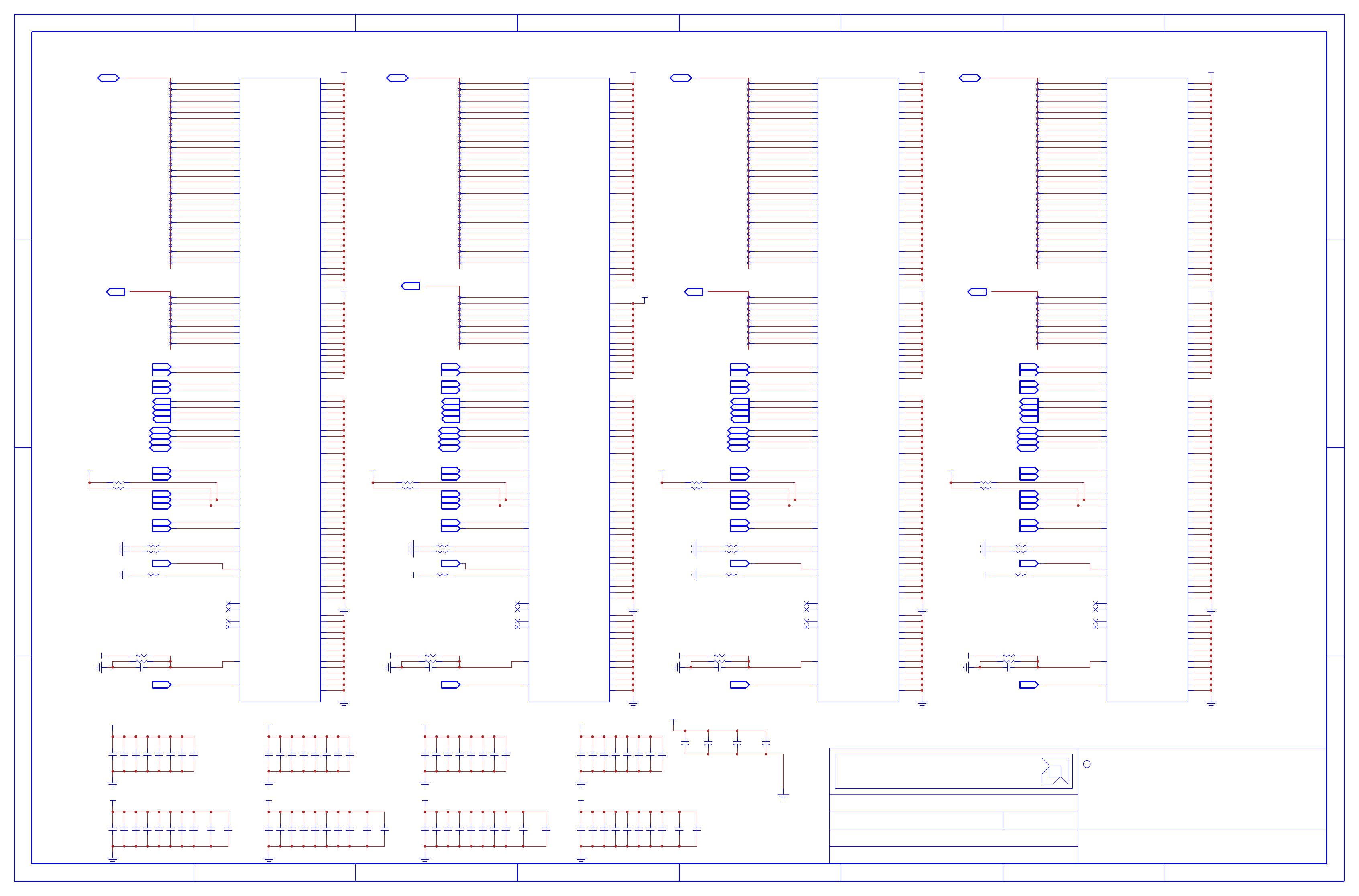
This AMD Board schematic and design is the exclusive property of AMD, and
DATE:
SHEET:
Advanced Micro Devices
2
3
345
6
6
7
7
8
8
C
5
CONFIDENTIAL AND PROPRIETARY TO ADVANCED MICRO DEVICES INC.
C
BB
A
1
DD
C
A
4
REV:
SHEET NUMBER:
DOCUMENT NUMBER:
OF
1
prohibited. Use of this schematic and design for any purpose other than
for evaluation purposes. Further distribution or disclosure is strictly
is provided only to entities under a non-disclosure agreement with AMD
2
schematic and design, including, not limited to, any implied warranty
AMD makes no representations or warranties of any kind regarding this
evaluation requires a Board Technology License Agreement with AMD.
of merchantability or fitness for a particular purpose, and disclaims
responsibility for any consequences resulting from use of the
information included herein.
TITLE:
+++
+
OUT
VSS_B5
VSS_B10
VSS_D10
VSS_G5
VSS_G10
VSS_H1
VSS_H14
VSS_K1
VSS_K14
VSS_L5
VSS_L10
VSS_P10
VSS_T5
VSS_T10
SEN
VSSQ_V14
VSSQ_V12
VSSQ_V3
VSSQ_V1
VSSQ_R14
VSSQ_R12
VSSQ_R11
VSSQ_R4
VSSQ_R3
VSSQ_R1
VSSQ_N1
VSSQ_N14
VSSQ_N12
VSSQ_N3
VSSQ_M10
VSSQ_M5
VSSQ_K13
VSSQ_K2
VSSQ_H13
VSSQ_H2
VSSQ_F10
VSSQ_F5
VSSQ_E14
VSSQ_E12
VSSQ_E3
VSSQ_E1
VSSQ_C14
VSSQ_C12
VSSQ_C11
VSSQ_C4
VSSQ_C3
VSSQ_C1
VSSQ_A14
VSSQ_A12
VSSQ_A3
VSSQ_A1
ZQ
VREFC
VDD_R10
VDD_R5
VDD_P11
VDD_L14
VDDQ_T14
VDDQ_T12
VDDQ_T3
VDDQ_T1
VDDQ_P14
VDDQ_P12
VDDQ_P3
VDDQ_P1
VDDQ_N10
VDDQ_N5
VDDQ_M14
VDDQ_M12
VDDQ_M3
VDDQ_M1
Vpp_NC1
Vpp_NC
WCK23#__WCK01#
WCK23__WCK01
WCK01#__WCK23#
WCK01__WCK23
RFU_A12_NC
VREFD2
VREFD1
MF
VDD_L11
VDD_L4
VDDQ_L13
VDDQ_L2
VDDQ_K12
VDDQ_K3
VDDQ_H12
VDDQ_H3
WE#__CS#
VDD_L1
VDD_G14
VDD_G11
VDD_G4
VDD_G1
VDD_D11
VDD_C10
VDD_C5
VDDQ_G13
VDDQ_G2
VDDQ_F14
VDDQ_F12
VDDQ_E10
DBI3#__DBI0#
DBI2#__DBI1#
DBI1#__DBI2#
DBI0#__DBI3#
EDC3__EDC0
EDC2__EDC1
EDC1__EDC2
EDC0__EDC3
VDDQ_E5
VDDQ_D14
VDDQ_D12
VDDQ_D3
VDDQ_D1
VDDQ_B14
VDDQ_B12
VDDQ_B3
VDDQ_B1
A5_BA1__A3_BA3
CK#
CK
VDDQ_F1
A1_A9__A6_A11
CKE#
RESET#
A2_BA0__A4_BA2
RAS#__CAS#
A6_A11__A1_A9
A7_A8__A0_A10
A4_BA2__A2_BA0
A0_A10__A7_A8
A3_BA3__A5_BA1
CS#__WE#
CAS#__RAS#
DQ0__DQ24
DQ1__DQ25
DQ2__DQ26
DQ3__DQ27
DQ4__DQ28
DQ5__DQ29
DQ6__DQ30
DQ7__DQ31
DQ8__DQ16
DQ9__DQ17
DQ10__DQ18
DQ11__DQ19
DQ12__DQ20
DQ13__DQ21
DQ14__DQ22
DQ15__DQ23
DQ16__DQ8
DQ17__DQ9
DQ18__DQ10
DQ19__DQ11
DQ20__DQ12
DQ21__DQ13
DQ22__DQ14
DQ23__DQ15
DQ24__DQ0
DQ25__DQ1
DQ26__DQ2
DQ27__DQ3
DQ28__DQ4
DQ29__DQ5
DQ30__DQ6
DQ31__DQ7
ABI#
VDDQ_F3
OUT
OUT
OUTBIBIBIBIININ
IN
VSS_B5
VSS_B10
VSS_D10
VSS_G5
VSS_G10
VSS_H1
VSS_H14
VSS_K1
VSS_K14
VSS_L5
VSS_L10
VSS_P10
VSS_T5
VSS_T10
SEN
VSSQ_V14
VSSQ_V12
VSSQ_V3
VSSQ_V1
VSSQ_R14
VSSQ_R12
VSSQ_R11
VSSQ_R4
VSSQ_R3
VSSQ_R1
VSSQ_N1
VSSQ_N14
VSSQ_N12
VSSQ_N3
VSSQ_M10
VSSQ_M5
VSSQ_K13
VSSQ_K2
VSSQ_H13
VSSQ_H2
VSSQ_F10
VSSQ_F5
VSSQ_E14
VSSQ_E12
VSSQ_E3
VSSQ_E1
VSSQ_C14
VSSQ_C12
VSSQ_C11
VSSQ_C4
VSSQ_C3
VSSQ_C1
VSSQ_A14
VSSQ_A12
VSSQ_A3
VSSQ_A1
ZQ
VREFC
VDD_R10
VDD_R5
VDD_P11
VDD_L14
VDDQ_T14
VDDQ_T12
VDDQ_T3
VDDQ_T1
VDDQ_P14
VDDQ_P12
VDDQ_P3
VDDQ_P1
VDDQ_N10
VDDQ_N5
VDDQ_M14
VDDQ_M12
VDDQ_M3
VDDQ_M1
Vpp_NC1
Vpp_NC
WCK23#__WCK01#
WCK23__WCK01
WCK01#__WCK23#
WCK01__WCK23
RFU_A12_NC
VREFD2
VREFD1
MF
VDD_L11
VDD_L4
VDDQ_L13
VDDQ_L2
VDDQ_K12
VDDQ_K3
VDDQ_H12
VDDQ_H3
WE#__CS#
VDD_L1
VDD_G14
VDD_G11
VDD_G4
VDD_G1
VDD_D11
VDD_C10
VDD_C5
VDDQ_G13
VDDQ_G2
VDDQ_F14
VDDQ_F12
VDDQ_E10
DBI3#__DBI0#
DBI2#__DBI1#
DBI1#__DBI2#
DBI0#__DBI3#
EDC3__EDC0
EDC2__EDC1
EDC1__EDC2
EDC0__EDC3
VDDQ_E5
VDDQ_D14
VDDQ_D12
VDDQ_D3
VDDQ_D1
VDDQ_B14
VDDQ_B12
VDDQ_B3
VDDQ_B1
A5_BA1__A3_BA3
CK#
CK
VDDQ_F1
A1_A9__A6_A11
CKE#
RESET#
A2_BA0__A4_BA2
RAS#__CAS#
A6_A11__A1_A9
A7_A8__A0_A10
A4_BA2__A2_BA0
A0_A10__A7_A8
A3_BA3__A5_BA1
CS#__WE#
CAS#__RAS#
DQ0__DQ24
DQ1__DQ25
DQ2__DQ26
DQ3__DQ27
DQ4__DQ28
DQ5__DQ29
DQ6__DQ30
DQ7__DQ31
DQ8__DQ16
DQ9__DQ17
DQ10__DQ18
DQ11__DQ19
DQ12__DQ20
DQ13__DQ21
DQ14__DQ22
DQ15__DQ23
DQ16__DQ8
DQ17__DQ9
DQ18__DQ10
DQ19__DQ11
DQ20__DQ12
DQ21__DQ13
DQ22__DQ14
DQ23__DQ15
DQ24__DQ0
DQ25__DQ1
DQ26__DQ2
DQ27__DQ3
DQ28__DQ4
DQ29__DQ5
DQ30__DQ6
DQ31__DQ7
ABI#
VDDQ_F3
ININININININININININININININININININBIBIBIBIOUT
OUT
OUT
OUTINININININININININBIBIBIBIOUT
OUT
OUT
OUTINININININININININBIBIBIBIOUT
OUT
OUT
OUTINININININININININBIBIBIBIOUT
OUT
OUT
OUTININININ
VSS_B5
VSS_B10
VSS_D10
VSS_G5
VSS_G10
VSS_H1
VSS_H14
VSS_K1
VSS_K14
VSS_L5
VSS_L10
VSS_P10
VSS_T5
VSS_T10
SEN
VSSQ_V14
VSSQ_V12
VSSQ_V3
VSSQ_V1
VSSQ_R14
VSSQ_R12
VSSQ_R11
VSSQ_R4
VSSQ_R3
VSSQ_R1
VSSQ_N1
VSSQ_N14
VSSQ_N12
VSSQ_N3
VSSQ_M10
VSSQ_M5
VSSQ_K13
VSSQ_K2
VSSQ_H13
VSSQ_H2
VSSQ_F10
VSSQ_F5
VSSQ_E14
VSSQ_E12
VSSQ_E3
VSSQ_E1
VSSQ_C14
VSSQ_C12
VSSQ_C11
VSSQ_C4
VSSQ_C3
VSSQ_C1
VSSQ_A14
VSSQ_A12
VSSQ_A3
VSSQ_A1
ZQ
VREFC
VDD_R10
VDD_R5
VDD_P11
VDD_L14
VDDQ_T14
VDDQ_T12
VDDQ_T3
VDDQ_T1
VDDQ_P14
VDDQ_P12
VDDQ_P3
VDDQ_P1
VDDQ_N10
VDDQ_N5
VDDQ_M14
VDDQ_M12
VDDQ_M3
VDDQ_M1
Vpp_NC1
Vpp_NC
WCK23#__WCK01#
WCK23__WCK01
WCK01#__WCK23#
WCK01__WCK23
RFU_A12_NC
VREFD2
VREFD1
MF
VDD_L11
VDD_L4
VDDQ_L13
VDDQ_L2
VDDQ_K12
VDDQ_K3
VDDQ_H12
VDDQ_H3
WE#__CS#
VDD_L1
VDD_G14
VDD_G11
VDD_G4
VDD_G1
VDD_D11
VDD_C10
VDD_C5
VDDQ_G13
VDDQ_G2
VDDQ_F14
VDDQ_F12
VDDQ_E10
DBI3#__DBI0#
DBI2#__DBI1#
DBI1#__DBI2#
DBI0#__DBI3#
EDC3__EDC0
EDC2__EDC1
EDC1__EDC2
EDC0__EDC3
VDDQ_E5
VDDQ_D14
VDDQ_D12
VDDQ_D3
VDDQ_D1
VDDQ_B14
VDDQ_B12
VDDQ_B3
VDDQ_B1
A5_BA1__A3_BA3
CK#
CK
VDDQ_F1
A1_A9__A6_A11
CKE#
RESET#
A2_BA0__A4_BA2
RAS#__CAS#
A6_A11__A1_A9
A7_A8__A0_A10
A4_BA2__A2_BA0
A0_A10__A7_A8
A3_BA3__A5_BA1
CS#__WE#
CAS#__RAS#
DQ0__DQ24
DQ1__DQ25
DQ2__DQ26
DQ3__DQ27
DQ4__DQ28
DQ5__DQ29
DQ6__DQ30
DQ7__DQ31
DQ8__DQ16
DQ9__DQ17
DQ10__DQ18
DQ11__DQ19
DQ12__DQ20
DQ13__DQ21
DQ14__DQ22
DQ15__DQ23
DQ16__DQ8
DQ17__DQ9
DQ18__DQ10
DQ19__DQ11
DQ20__DQ12
DQ21__DQ13
DQ22__DQ14
DQ23__DQ15
DQ24__DQ0
DQ25__DQ1
DQ26__DQ2
DQ27__DQ3
DQ28__DQ4
DQ29__DQ5
DQ30__DQ6
DQ31__DQ7
ABI#
VDDQ_F3
8
7
6
345
2
1
C
A
(5) GDDR5 MEMORY CH A/B
(5) GDDR5 MEMORY CH A/B
DQA0_<31..0>
3 5
3 5
3 5
3 5
+MVDD +MVDD +MVDD
+MVDD +MVDD +MVDD
R2001
R2001
R2000
R2000
DQA0_<31..0>
3 5
3 5
3 5
3 5
3 5
3 5
3 5
3 5
3 5
3 5
3 5
3 5
3 5
3 5
3 5
3 5
3 5
3 5
3 5
3 5
3 5
3 5
3 5
3 5
3 5
3 5
3 5 3 5
3 5 3 5
3 5
3 5
3 5
3 5
3 5
3 5
3 5
3 5
3 5
3 5
3 5
3 5
3 5
3 5
3 5
3 5
3 5
3 5
3 5
3 5
3 5
3 5
3 5
3 5
3 5
3 5
3 5
3 5
3 5
3 5
3 5
3 5
3 5
3 5
MAA0_<8..0>
MAA0_<8..0>
OUT
3 5
3 5
3 5
3 5
3 5
3 5
3 5
3 5
3 5
3 5
3 5
3 5
3 5
3 5
3
3
IN
3
3
IN
3
3
IN
3
3
IN
3
3
OUT
3
3
OUT
3
3
OUT
3
3
OUT
3
3
BI
3
3
BI
3
3
BI
3
3
BI
3
3
IN
3
3
IN
1%60.4R
1%60.4R
1%60.4R
1%60.4R
3
3
IN
3
3
IN
3
3
IN
3
3
IN
3
3
IN
R2002
R2002
R2003
R2003
3 5
3 5
IN
R2004
R2004
R2009
R2009
R2010
R2010
C2005
C2005
C2007
C2007
0.1uF
0.1uF
+MVDD +MVDD
+MVDD +MVDD
C2019
C2019
1uF
1uF
C2008
C2008
0.1uF
0.1uF
C2020
C2020
1uF
1uF
1uF
1uF
3
3
IN IN
C2009
C2009
C2010
C2010
0.1uF
0.1uF
0.1uF
0.1uF
C2023
C2024
C2023
C2024
1uF
1uF
1uF
1uF
28
28
31
31
29
29
30
30
27
27
26
26
24
24
25
25
17
17
23
23
16
16
22
22
18
18
21
21
19
19
20
20
5
5
6
6
4
4
7
7
3
3
2
2
1
1
0
0
11
11
10
10
8
8
9
9
12
12
13
13
15
15
14
14
8
8
7
7
6
6
5
5
4
4
3
3
2
2
1
1
0
0
120R 1%
120R 1%
5%1K
5%1K
5%1K
5%1K
1%2.37K
1%2.37K
1%5.49K
1%5.49K
6.3V
6.3V
C2013
C2012
C2013
C2012
0.1uF
0.1uF
0.1uF
0.1uF
C2026
C2026
C2025
C2025
1uF
1uF
1uF
1uF
5
5
3
3
DQA0_<28>
DQA0_<28>
DQA0_<31>
DQA0_<31>
DQA0_<29>
DQA0_<29>
DQA0_<30>
DQA0_<30>
DQA0_<27>
DQA0_<27>
DQA0_<26>
DQA0_<26>
DQA0_<24>
DQA0_<24>
DQA0_<25>
DQA0_<25>
DQA0_<17>
DQA0_<17>
DQA0_<23>
DQA0_<23>
DQA0_<16>
DQA0_<16>
DQA0_<22>
DQA0_<22>
DQA0_<18>
DQA0_<18>
DQA0_<21>
DQA0_<21>
DQA0_<19>
DQA0_<19> DQA1_<14>
DQA0_<20>
DQA0_<20>
DQA0_<5>
DQA0_<5>
DQA0_<6>
DQA0_<6>
DQA0_<4>
DQA0_<4>
DQA0_<7>
DQA0_<7>
DQA0_<3>
DQA0_<3>
DQA0_<2>
DQA0_<2>
DQA0_<1>
DQA0_<1>
DQA0_<0>
DQA0_<0>
DQA0_<11>
DQA0_<11>
DQA0_<10>
DQA0_<10>
DQA0_<8>
DQA0_<8>
DQA0_<9>
DQA0_<9>
DQA0_<12>
DQA0_<12>
DQA0_<13>
DQA0_<13>
DQA0_<15>
DQA0_<15>
DQA0_<14>
DQA0_<14>
5
5
MAA0_<8>
3
3
MAA0_<8>
MAA0_<7>
MAA0_<7>
MAA0_<6>
MAA0_<6>
MAA0_<5>
MAA0_<5>
MAA0_<4>
MAA0_<4>
MAA0_<3>
MAA0_<3>
MAA0_<1>
MAA0_<1>
MAA0_<0>
MAA0_<0>
WCKA0_0
WCKA0_0
WCKA0b_0
WCKA0b_0
WCKA0_1
WCKA0_1
WCKA0b_1
WCKA0b_1
EDCA0_3
EDCA0_3
EDCA0_2
EDCA0_2
EDCA0_0
EDCA0_0
EDCA0_1
EDCA0_1
DDBIA0_3
DDBIA0_3
DDBIA0_2
DDBIA0_2
DDBIA0_0
DDBIA0_0
DDBIA0_1
DDBIA0_1
RASA0b
RASA0b
CASA0b
CASA0b
CKEA0
CKEA0
CLKA0b
CLKA0b
CLKA0
CLKA0
CSA0b_0
CSA0b_0
WEA0b
WEA0b
ZQ_A0
ZQ_A0
SEN_A0
SEN_A0
DRAM_RST1
DRAM_RST1
MF_A0
MF_A0
VREFC_A0
VREFC_A0
ADBIA0
ADBIA0
C2015
C2015
C2014
C2014
0.1uF
0.1uF
0.1uF
0.1uF
C2029
C2028
C2029
C2028
1uF
1uF
1uF
1uF
22uF
22uF
4V
4V
2 1
2 1
C2040
C2040
M13
M13
M11
M11
N13
N13
N11
N11
T13
T13
T11
T11
V13
V13
V11
V11
F13
F13
F11
F11
E13
E13
E11
E11
B13
B13
B11
B11
A13
A13
A11
A11
K10
K10
K11
K11
H10
H10
H11
H11
R13
R13
C13
C13
P13
P13
D13
D13
J11
J11
J12
J12
G12
G12
L12
L12
J13
J13
J10
J10
A10
A10
V10
V10
J14
J14
M2
M2
M4
M4
N2
N2
N4
N4
T2
T2
T4
T4
V2
V2
V4
V4
F2
F2
F4
F4
E2
E2
E4
E4
B2
B2
B4
B4
A2
A2
A4
A4
J5
J5
K4
K4
K5
K5
H5
H5
H4
H4
D4
D4
D5
D5
P4
P4
P5
P5
R2
R2
C2
C2
P2
P2
D2
D2
G3
G3
L3
L3
J3
J3
J2
J2
J1
J1
A5
A5
V5
V5
J4
J4
22uF
22uF
4V
4V
2 1
2 1
8
DQ31__DQ7
DQ30__DQ6
DQ29__DQ5
DQ28__DQ4
DQ27__DQ3
DQ26__DQ2
DQ25__DQ1
DQ24__DQ0
DQ23__DQ15
DQ22__DQ14
DQ21__DQ13
DQ20__DQ12
DQ19__DQ11
DQ18__DQ10
DQ17__DQ9
DQ16__DQ8
DQ15__DQ23
DQ14__DQ22
DQ13__DQ21
DQ12__DQ20
DQ11__DQ19
DQ10__DQ18
DQ9__DQ17
DQ8__DQ16
DQ7__DQ31
DQ6__DQ30
DQ5__DQ29
DQ4__DQ28
DQ3__DQ27
DQ2__DQ26
DQ1__DQ25
DQ0__DQ24
RFU_A12_NC
A7_A8__A0_A10
A6_A11__A1_A9
A5_BA1__A3_BA3
A4_BA2__A2_BA0
A3_BA3__A5_BA1
A2_BA0__A4_BA2
A1_A9__A6_A11
A0_A10__A7_A8
WCK01__WCK23
WCK01#__WCK23#
WCK23__WCK01
WCK23#__WCK01#
EDC3__EDC0
EDC2__EDC1
EDC1__EDC2
EDC0__EDC3
DBI3#__DBI0#
DBI2#__DBI1#
DBI1#__DBI2#
DBI0#__DBI3#
RAS#__CAS#
CAS#__RAS#
CKE#
CK#
CK
CS#__WE#
WE#__CS#
ZQ
SEN
RESET#
MF
Vpp_NC
Vpp_NC1
VREFD1
VREFD2
VREFC
ABI#
+MVDD
+MVDD
C2041
C2041
23CNOPN001
23CNOPN001
U2000
U2000
C2107C2118
C2107C2118
1uF 0.1uF
1uF 0.1uF
7
C2108
C2108
0.1uF
0.1uF
C2119
C2119
1uF
1uF
VDDQ_B1
VDDQ_B3
VDDQ_B12
VDDQ_B14
VDDQ_D1
VDDQ_D3
VDDQ_D12
VDDQ_D14
VDDQ_E5
VDDQ_E10
VDDQ_F1
VDDQ_F3
VDDQ_F12
VDDQ_F14
VDDQ_G2
VDDQ_G13
VDDQ_H3
VDDQ_H12
VDDQ_K3
VDDQ_K12
VDDQ_L2
VDDQ_L13
VDDQ_M1
VDDQ_M3
VDDQ_M12
VDDQ_M14
VDDQ_N5
VDDQ_N10
VDDQ_P1
VDDQ_P3
VDDQ_P12
VDDQ_P14
VDDQ_T1
VDDQ_T3
VDDQ_T12
VDDQ_T14
VDD_C5
VDD_C10
VDD_D11
VDD_G1
VDD_G4
VDD_G11
VDD_G14
VDD_L1
VDD_L4
VDD_L11
VDD_L14
VDD_P11
VDD_R5
VDD_R10
VSSQ_A1
VSSQ_A3
VSSQ_A12
VSSQ_A14
VSSQ_C1
VSSQ_C3
VSSQ_C4
VSSQ_C11
VSSQ_C12
VSSQ_C14
VSSQ_E1
VSSQ_E3
VSSQ_E12
VSSQ_E14
VSSQ_F5
VSSQ_F10
VSSQ_H2
VSSQ_H13
VSSQ_K2
VSSQ_K13
VSSQ_M5
VSSQ_M10
VSSQ_N1
VSSQ_N3
VSSQ_N12
VSSQ_N14
VSSQ_R1
VSSQ_R3
VSSQ_R4
VSSQ_R11
VSSQ_R12
VSSQ_R14
VSSQ_V1
VSSQ_V3
VSSQ_V12
VSSQ_V14
VSS_B5
VSS_B10
VSS_D10
VSS_G5
VSS_G10
VSS_H1
VSS_H14
VSS_K1
VSS_K14
VSS_L5
VSS_L10
VSS_P10
VSS_T5
VSS_T10
C2110
C2109
C2110
C2109
0.1uF
0.1uF
0.1uF
0.1uF
C2121
C2120
C2121
C2120
1uF
1uF
1uF
1uF
B1
B1
B3
B3
B12
B12
B14
B14
D1
D1
D3
D3
D12
D12
D14
D14
E5
E5
E10
E10
F1
F1
F3
F3
F12
F12
F14
F14
G2
G2
G13
G13
H3
H3
H12
H12
K3
K3
K12
K12
L2
L2
L13
L13
M1
M1
M3
M3
M12
M12
M14
M14
N5
N5
N10
N10
P1
P1
P3
P3
P12
P12
P14
P14
T1
T1
T3
T3
T12
T12
T14
T14
C5
C5
C10
C10
D11
D11
G1
G1
G4
G4
G11
G11
G14
G14
L1
L1
L4
L4
L11
L11
L14
L14
P11
P11
R5
R5
R10
R10
A1
A1
A3
A3
A12
A12
A14
A14
C1
C1
C3
C3
C4
C4
C11
C11
C12
C12
C14
C14
E1
E1
E3
E3
E12
E12
E14
E14
F5
F5
F10
F10
H2
H2
H13
H13
K2
K2
K13
K13
M5
M5
M10
M10
N1
N1
N3
N3
N12
N12
N14
N14
R1
R1
R3
R3
R4
R4
R11
R11
R12
R12
R14
R14
V1
V1
V3
V3
V12
V12
V14
V14
B5
B5
B10
B10
D10
D10
G5
G5
G10
G10
H1
H1
H14
H14
K1
K1
K14
K14
L5
L5
L10
L10
P10
P10
T5
T5
T10
T10
C2112
C2112
0.1uF
0.1uF
C2122
C2122
1uF
1uF
+MVDD
+MVDD
+MVDD
+MVDD
C2115
C2115
0.1uF
0.1uF
C2126
C2126
1uF
1uF
C2116
C2116
0.1uF
0.1uF
C2127
C2127
1uF
1uF
C2117
C2117
0.1uF
0.1uF
C2129
C2129
1uF
1uF
2 1
2 1
+MVDD+MVDD
+MVDD+MVDD
C2140
C2140
22uF
22uF
3 5
3 5
R2101
R2101
R2100
R2100
22uF
22uF
4V
4V
2 1
2 1
+MVDD
B1
B1
B3
B3
B12
B12
B14
B14
D1
D1
D3
D3
D12
D12
D14
D14
E5
E5
E10
E10
F1
F1
F3
F3
F12
F12
F14
F14
G2
G2
G13
G13
H3
H3
H12
H12
K3
K3
K12
K12
L2
L2
L13
L13
M1
M1
M3
M3
M12
M12
M14
M14
N5
N5
N10
N10
P1
P1
P3
P3
P12
P12
P14
P14
T1
T1
T3
T3
T12
T12
T14
T14
C5
C5
C10
C10
D11
D11
G1
G1
G4
G4
G11
G11
G14
G14
L1
L1
L4
L4
L11
L11
L14
L14
P11
P11
R5
R5
R10
R10
A1
A1
A3
A3
A12
A12
A14
A14
C1
C1
C3
C3
C4
C4
C11
C11
C12
C12
C14
C14
E1
E1
E3
E3
E12
E12
E14
E14
F5
F5
F10
F10
H2
H2
H13
H13
K2
K2
K13
K13
M5
M5
M10
M10
N1
N1
N3
N3
N12
N12
N14
N14
R1
R1
R3
R3
R4
R4
R11
R11
R12
R12
R14
R14
V1
V1
V3
V3
V12
V12
V14
V14
B5
B5
B10
B10
D10
D10
G5
G5
G10
G10
H1
H1
H14
H14
K1
K1
K14
K14
L5
L5
L10
L10
P10
P10
T5
T5
T10
T10
C2309
C2309
0.1uF
0.1uF
C2322
C2322
1uF
1uF
+MVDD
C2311
C2311
0.1uF
0.1uF
C2323
C2323
1uF
1uF
+MVDD
+MVDD
C2312
C2312
0.1uF
0.1uF
C2324
C2324
1uF
1uF
C2314
C2314
0.1uF
0.1uF
C2325
C2325
1uF
1uF
+MVDD
+MVDD
+MVDD
+MVDD
C2316
C2316
0.1uF
0.1uF
C2326
C2326
1uF
1uF
+MVDD
+MVDD
C2317
C2317
0.1uF
0.1uF
C2328
C2328
1uF
1uF
3 5
3 5
OUT
R2201
R2201
R2200
R2200
12
12
+ +++
C2361
C2361 C2364C2363C2362
470uF
470uF
2V
2V
C2340
C2340
22uF
22uF
4V
4V
2 1
2 1
DQB0_<31..0>
DQB0_<31..0>
3 5
3 5
3 5
5
3
3 5
3 5
3 5
3 5
3 5
3 5
3 5
3 5
3 5
3 5
3 5
3 5
3 5
3 5
3 5
3 5
3 5
3 5
3 5
3 5
3 5
3 5
3 5
3 5
3 5
3 5
MAB0_<8..0>
MAB0_<8..0>
3 5
3 5
3 5
3 5
3 5
3 5
3 5
3 5
3 5
3 5
3 5 3 5
3 5 3 5
3 5
3 5
3 5
3 5
3
3
IN
3
3
IN
3
3
IN
3
3
IN
3
3
OUT
3
3
OUT
3
3
OUT
3
3
OUT
3
3
BI
3
3
BI
3
3
BI
3
3
BI
3
3
IN
3
3
IN
1%60.4R
1%60.4R
3
3
IN
3
3
IN
3
3
IN
3
3
IN
3
3
IN
3 5
3 5
IN
2.37K
2.37K
1uF
1uF
3
3
IN
Reserved. detail please check BOM
Reserved. detail please check BOM
12
12
C2362
470uF
470uF
2V
2V
C2363
470uF
470uF
2V
2V
R2209
R2209
R2210
R2210
22uF
22uF
4V
4V
2 1
2 1
C2205
C2205
60.4R 1%
60.4R 1%
R2202
R2202
R2203
R2203
R2204
R2204
12
12
C2341
C2341
1%
1%
1%5.49K
1%5.49K
6.3V
6.3V
13
13
15
15
12
12
14
14
11
11
8
8
10
10
9
9
0
0
7
7
1
1
6
6
3
3
5
5
2
2
4
4
30
30
29
29
28
28
31
31
27
27
26
26
24
24
25
25
19
19
18
18
17
17
16
16
20
20
21
21
22
22
23
23
8
8
7
7
6
6
5
5
4
4
3
3
2
2
1
1
0
0
1%120R
1%120R
5%1K
5%1K
5%1K
5%1K
3 5
3 5
3 5
3 5
3 5
3 5
3 5
3 5
3 5
3 5
3 5
3 5
3 5
3 5
3 5
3 5
3 5
3 5
3 5
3 5
3 5
3 5
3 5
3 5
3 5
3 5
3 5
3 5
DQB0_<4>
DQB0_<4>
DQB0_<30>
DQB0_<30>
DQB0_<29>
DQB0_<29>
DQB0_<28>
DQB0_<28>
DQB0_<31>
DQB0_<31>
DQB0_<27>
DQB0_<27>
DQB0_<26>
DQB0_<26>
DQB0_<24>
DQB0_<24>
3 5
3 5
3 5
3 5
DQB0_<18>
DQB0_<18>
DQB0_<17>
DQB0_<17>
DQB0_<16>
DQB0_<16>
DQB0_<20>
DQB0_<20>
DQB0_<21>
DQB0_<21>
DQB0_<22>
DQB0_<22>
DQB0_<23>
DQB0_<23>
5
5
3
3
MAB0_<8>
MAB0_<8>
MAB0_<7>
MAB0_<7>
MAB0_<6>
MAB0_<6>
MAB0_<5>
MAB0_<5>
MAB0_<4>
MAB0_<4>
MAB0_<3>
MAB0_<3>
MAB0_<2>MAA0_<2>
MAB0_<2>MAA0_<2>
MAB0_<1>
MAB0_<1>
MAB0_<0>
MAB0_<0>
WCKB0_1
WCKB0_1
WCKB0b_1
WCKB0b_1
WCKB0_0
WCKB0_0
WCKB0b_0
WCKB0b_0
DDBIB0_1
DDBIB0_1
DDBIB0_0
DDBIB0_0
DDBIB0_3
DDBIB0_3
DDBIB0_2
DDBIB0_2
RASB0b
RASB0b
CASB0b
CASB0b
CKEB0
CKEB0
CLKB0b
CLKB0b
CLKB0
CLKB0
CSB0b_0
CSB0b_0
WEB0b
WEB0b
ZQ_B0
ZQ_B0
SEN_B0
SEN_B0
DRAM_RST1
DRAM_RST1
MF_B0
MF_B0
VREFC_B0
VREFC_B0
ADBIB0
ADBIB0
12
12
4
DQB0_<13>
DQB0_<13>
DQB0_<15>
DQB0_<15>
DQB0_<12>
DQB0_<12>
DQB0_<14>
DQB0_<14>
DQB0_<11>
DQB0_<11>
DQB0_<8>
DQB0_<8>
DQB0_<10>
DQB0_<10>
DQB0_<9>
DQB0_<9>
DQB0_<0>
DQB0_<0>
DQB0_<7>
DQB0_<7>
DQB0_<1>
DQB0_<1>
DQB0_<6>
DQB0_<6>
DQB0_<3>
DQB0_<3>
DQB0_<5>
DQB0_<5>
DQB0_<2>
3 5
3 5
DQB0_<2>
DQB0_<25>
DQB0_<25>
DQB0_<19>
DQB0_<19>
EDCB0_1
EDCB0_1
EDCB0_0
EDCB0_0
EDCB0_3
EDCB0_3
EDCB0_2
EDCB0_2
C2364
470uF
470uF
2V
2V
M2
M2
DQ31__DQ7
M4
M4
DQ30__DQ6
N2
N2
DQ29__DQ5
N4
N4
DQ28__DQ4
T2
T2
DQ27__DQ3
T4
T4
DQ26__DQ2
V2
V2
DQ25__DQ1
V4
V4
DQ24__DQ0
M13
M13
DQ23__DQ15
M11
M11
DQ22__DQ14
N13
N13
DQ21__DQ13
N11
N11
DQ20__DQ12
T13
T13
DQ19__DQ11
T11
T11
DQ18__DQ10
V13
V13
DQ17__DQ9
V11
V11
DQ16__DQ8
F13
F13
DQ15__DQ23
F11
F11
DQ14__DQ22
E13
E13
DQ13__DQ21
E11
E11
DQ12__DQ20
B13
B13
DQ11__DQ19
B11
B11
DQ10__DQ18
A13
A13
DQ9__DQ17
A11
A11
DQ8__DQ16
F2
F2
DQ7__DQ31
F4
F4
DQ6__DQ30
E2
E2
DQ5__DQ29
E4
E4
DQ4__DQ28
B2
B2
DQ3__DQ27
B4
B4
DQ2__DQ26
A2
A2
DQ1__DQ25
A4
A4
DQ0__DQ24
J5
J5
RFU_A12_NC
K4
K4
A7_A8__A0_A10
K5
K5
A6_A11__A1_A9
K10
K10
A5_BA1__A3_BA3
K11
K11
A4_BA2__A2_BA0
H10
H10
A3_BA3__A5_BA1
H11
H11
A2_BA0__A4_BA2
H5
H5
A1_A9__A6_A11
H4
H4
A0_A10__A7_A8
D4
D4
WCK01__WCK23
D5
D5
WCK01#__WCK23#
P4
P4
WCK23__WCK01
P5
P5
WCK23#__WCK01#
R2
R2
EDC3__EDC0
R13
R13
EDC2__EDC1
C13
C13
EDC1__EDC2
C2
C2
EDC0__EDC3
P2
P2
DBI3#__DBI0#
P13
P13
DBI2#__DBI1#
D13
D13
DBI1#__DBI2#
D2
D2
DBI0#__DBI3#
G3
G3
RAS#__CAS#
L3
L3
CAS#__RAS#
J3
J3
CKE#
J11
J11
CK#
J12
J12
CK
G12
G12
CS#__WE#
L12
L12
WE#__CS#
J13
J13
ZQ
J10
J10
SEN
J2
J2
RESET#
J1
J1
MF
A5
A5
Vpp_NC
V5
V5
Vpp_NC1
A10
A10
VREFD1
V10
V10
VREFD2
J14
J14
VREFC
J4
J4
ABI#
AMD - PLATFORM HARDWARE ENG
AMD - PLATFORM HARDWARE ENG
#48, No.1387, ZHANGDONG ROAD
#48, No.1387, ZHANGDONG ROAD
SHANGHAI, CHINA 201203
SHANGHAI, CHINA 201203
SHEET:
DATE:
SHEET NUMBER:
DOCUMENT NUMBER:
23CNOPN001
23CNOPN001
U2200
U2200
VDDQ_B1
VDDQ_B3
VDDQ_B12
VDDQ_B14
VDDQ_D1
VDDQ_D3
VDDQ_D12
VDDQ_D14
VDDQ_E5
VDDQ_E10
VDDQ_F1
VDDQ_F3
VDDQ_F12
VDDQ_F14
VDDQ_G2
VDDQ_G13
VDDQ_H3
VDDQ_H12
VDDQ_K3
VDDQ_K12
VDDQ_L2
VDDQ_L13
VDDQ_M1
VDDQ_M3
VDDQ_M12
VDDQ_M14
VDDQ_N5
VDDQ_N10
VDDQ_P1
VDDQ_P3
VDDQ_P12
VDDQ_P14
VDDQ_T1
VDDQ_T3
VDDQ_T12
VDDQ_T14
VDD_C5
VDD_C10
VDD_D11
VDD_G1
VDD_G4
VDD_G11
VDD_G14
VDD_L1
VDD_L4
VDD_L11
VDD_L14
VDD_P11
VDD_R5
VDD_R10
VSSQ_A1
VSSQ_A3
VSSQ_A12
VSSQ_A14
VSSQ_C1
VSSQ_C3
VSSQ_C4
VSSQ_C11
VSSQ_C12
VSSQ_C14
VSSQ_E1
VSSQ_E3
VSSQ_E12
VSSQ_E14
VSSQ_F5
VSSQ_F10
VSSQ_H2
VSSQ_H13
VSSQ_K2
VSSQ_K13
VSSQ_M5
VSSQ_M10
VSSQ_N1
VSSQ_N3
VSSQ_N12
VSSQ_N14
VSSQ_R1
VSSQ_R3
VSSQ_R4
VSSQ_R11
VSSQ_R12
VSSQ_R14
VSSQ_V1
VSSQ_V3
VSSQ_V12
VSSQ_V14
VSS_B5
VSS_B10
VSS_D10
VSS_G5
VSS_G10
VSS_H1
VSS_H14
VSS_K1
VSS_K14
VSS_L5
VSS_L10
VSS_P10
VSS_T5
VSS_T10
GDDR5 MEM CH AB
GDDR5 MEM CH AB
Wed Apr 13 17:02:16 2016
Wed Apr 13 17:02:16 2016
23CNOPN001
23CNOPN001
U2100
2 1
2 1
22uF22uF
22uF22uF
4V
4V
C2241
C2241
U2100
+MVDD
+MVDD
+MVDD
+MVDD
VDDQ_B1
VDDQ_B3
VDDQ_B12
VDDQ_B14
VDDQ_D1
VDDQ_D3
VDDQ_D12
VDDQ_D14
VDDQ_E5
VDDQ_E10
VDDQ_F1
VDDQ_F3
VDDQ_F12
VDDQ_F14
VDDQ_G2
VDDQ_G13
VDDQ_H3
VDDQ_H12
VDDQ_K3
VDDQ_K12
VDDQ_L2
VDDQ_L13
VDDQ_M1
VDDQ_M3
VDDQ_M12
VDDQ_M14
VDDQ_N5
VDDQ_N10
VDDQ_P1
VDDQ_P3
VDDQ_P12
VDDQ_P14
VDDQ_T1
VDDQ_T3
VDDQ_T12
VDDQ_T14
VDD_C5
VDD_C10
VDD_D11
VDD_G1
VDD_G4
VDD_G11
VDD_G14
VDD_L1
VDD_L4
VDD_L11
VDD_L14
VDD_P11
VDD_R5
VDD_R10
VSSQ_A1
VSSQ_A3
VSSQ_A12
VSSQ_A14
VSSQ_C1
VSSQ_C3
VSSQ_C4
VSSQ_C11
VSSQ_C12
VSSQ_C14
VSSQ_E1
VSSQ_E3
VSSQ_E12
VSSQ_E14
VSSQ_F5
VSSQ_F10
VSSQ_H2
VSSQ_H13
VSSQ_K2
VSSQ_K13
VSSQ_M5
VSSQ_M10
VSSQ_N1
VSSQ_N3
VSSQ_N12
VSSQ_N14
VSSQ_R1
VSSQ_R3
VSSQ_R4
VSSQ_R11
VSSQ_R12
VSSQ_R14
VSSQ_V1
VSSQ_V3
VSSQ_V12
VSSQ_V14
VSS_B5
VSS_B10
VSS_D10
VSS_G5
VSS_G10
VSS_H1
VSS_H14
VSS_K1
VSS_K14
VSS_L5
VSS_L10
VSS_P10
VSS_T5
VSS_T10
C2306
C2306
C2308
C2308
0.1uF
0.1uF
0.1uF
0.1uF
C2319
C2321
C2319
C2321
1uF
1uF
1uF
1uF
5
DQA1_<31..0>
DQA1_<31..0>
3 5
3 5
3 5
3 5
3 5
3 5
3 5
3 5
3 5
3 5
3 5
3 5
3 5
3 5
3 5
3 5
3 5
3 5
3 5
3 5
3 5
3 5
3 5
3 5
3 5
3 5
3 5
3 5
3 5
3 5
3 5
3 5
3 5
3 5
3 5
3 5
3 5
3 5
3 5
3 5
3 5
3 5
3 5
3 5
3 5
3 5
3 5
3 5
3 5
3 5
3 5
3 5
3 5
3 5
3 5
3 5
3 5
3 5
MAA1_<8..0>
OUT
MAA1_<8..0>
3
3
3
3
3
3
3
3
3
3
3
3
3
3
3
3
3
3
3
3
3
3
3
3
3
3
3
3
60.4R
60.4R
60.4R 1%
60.4R 1%
3
3
3
3
3
3
3
3
3
3
R2102
R2102
R2103
R2103
3 5
3 5
3 5
3 5
3 5
3 5
3 5
3 5
3 5
3 5
3 5
3 5
3 5
3 5
3 5
3 5
IN
IN
IN
IN
OUT
OUT
OUT
OUT
BI
BI
BI
BI
IN
IN
1%
1%
IN
IN
IN
IN
IN
3 5
3 5
IN
R2104
+MVDD
+MVDD
C2141
C2141
R2104
R2109
R2109
R2110
R2110
C2105 C2305
C2105 C2305
3
3
+MVDD+MVDD+MVDD
+MVDD+MVDD+MVDD
C2206
C2206
C2208
C2208
0.1uF
0.1uF
0.1uF
0.1uF
C2219
C2220
C2219
C2220
1uF
1uF
1uF
1uF
1K 5%
1K 5%
1%2.37K
1%2.37K
1%5.49K
1%5.49K
6.3V
6.3V
C2209
C2209
0.1uF
0.1uF
C2223
C2223
1uF
1uF
5
5
6
6
4
4
7
7
3
3
2
2
1
1
0
0
11
11
8
8
10
10
9
9
12
12
13
13
14
14
15
15
31
31
24
24
29
29
25
25
28
28
26
26
30
30
27
27
18
18
17
17
19
19
16
16
21
21
23
23
20
20
22
22
8
8
0
0
1
1
3
3
2
2
5
5
4
4
6
6
7
7
3 5
3 5
5%1K
5%1K
C2211
C2211
0.1uF
0.1uF
C2226
C2226
1uF
1uF
5
5
3
3
DQA1_<5>
DQA1_<5>
DQA1_<6>
DQA1_<6>
DQA1_<4>
DQA1_<4>
DQA1_<7>
DQA1_<7>
DQA1_<3>
DQA1_<3>
DQA1_<2>
DQA1_<2>
DQA1_<1>
DQA1_<1>
DQA1_<0>
DQA1_<0>
DQA1_<11>
DQA1_<11>
DQA1_<8>
DQA1_<10>
DQA1_<10>
DQA1_<9>
DQA1_<9>
DQA1_<12>
DQA1_<12>
DQA1_<13>
DQA1_<13>
DQA1_<14>
DQA1_<15>
DQA1_<15>
DQA1_<31>
DQA1_<31>
DQA1_<24>
DQA1_<24>
DQA1_<29>
DQA1_<29>
DQA1_<25>
DQA1_<25>
DQA1_<28>
DQA1_<28>
DQA1_<26>
DQA1_<26>
DQA1_<30>
DQA1_<30>
DQA1_<27>
DQA1_<27>
DQA1_<18>
DQA1_<18>
DQA1_<17>
DQA1_<17>
DQA1_<19>
DQA1_<19>
DQA1_<16>
DQA1_<16>
DQA1_<21>
DQA1_<21>
DQA1_<23>
DQA1_<23>
DQA1_<20>
DQA1_<20>
DQA1_<22>
DQA1_<22>
5
5
3
MAA1_<8>
3
MAA1_<8>
MAA1_<0>
MAA1_<0>
MAA1_<1>
MAA1_<1>
MAA1_<3>
MAA1_<3>
MAA1_<2>
MAA1_<2>
MAA1_<5>
MAA1_<5>
MAA1_<4>
MAA1_<4>
MAA1_<6>
MAA1_<6>
MAA1_<7>
MAA1_<7>
WCKA1_1
WCKA1_1
WCKA1b_1
WCKA1b_1
WCKA1_0
WCKA1_0
WCKA1b_0
WCKA1b_0
EDCA1_0
EDCA1_0
EDCA1_1
EDCA1_1
EDCA1_3
EDCA1_3
EDCA1_2
EDCA1_2
DDBIA1_0
DDBIA1_0
DDBIA1_1
DDBIA1_1
DDBIA1_3
DDBIA1_3
DDBIA1_2
DDBIA1_2
CASA1b
CASA1b
RASA1b
RASA1b
CKEA1
CKEA1
CLKA1b
CLKA1b
CLKA1
CLKA1
WEA1b
WEA1b
CSA1b_0
CSA1b_0
ZQ_A1
ZQ_A1
1%120R
1%120R
SEN_A1
SEN_A1
DRAM_RST1
DRAM_RST1
MF_A1
MF_A1
VREFC_A1
VREFC_A1
ADBIA1
ADBIA1
C2212
C2212
0.1uF
0.1uF
C2227
C2227
1uF
1uF
C2213
C2213
0.1uF
0.1uF
C2228
C2228
1uF
1uF
C2214
C2214
0.1uF
0.1uF
C2229
C2229
1uF
1uF
M2
M2
M4
M4
N2
N2
N4
N4
T2
T2
T4
T4
V2
V2
V4
V4
M13
M13
M11
M11
N13
N13
N11
N11
T13
T13
T11
T11
V13
V13
V11
V11
F13
F13
F11
F11
E13
E13
E11
E11
B13
B13
B11
B11
A13
A13
A11
A11
F2
F2
F4
F4
E2
E2
E4
E4
B2
B2
B4
B4
A2
A2
A4
A4
J5
J5
K4
K4
K5
K5
K10
K10
K11
K11
H10
H10
H11
H11
H5
H5
H4
H4
D4
D4
D5
D5
P4
P4
P5
P5
R2
R2
R13
R13
C13
C13
C2
C2
P2
P2
P13
P13
D13
D13
D2
D2
G3
G3
L3
L3
J3
J3
J11
J11
J12
J12
G12
G12
L12
L12
J13
J13
J10
J10
J2
J2
J1
J1
A5
A5
V5
V5
A10
A10
V10
V10
J14
J14
J4
J4
C2218
C2218
0.1uF
0.1uF
C2230
C2230
1uF
1uF
4V4V
4V4V
2 1
2 1
DQ31__DQ7
DQ30__DQ6
DQ29__DQ5
DQ28__DQ4
DQ27__DQ3
DQ26__DQ2
DQ25__DQ1
DQ24__DQ0
DQ23__DQ15
DQ22__DQ14
DQ21__DQ13
DQ20__DQ12
DQ19__DQ11
DQ18__DQ10
DQ17__DQ9
DQ16__DQ8
DQ15__DQ23
DQ14__DQ22
DQ13__DQ21
DQ12__DQ20
DQ11__DQ19
DQ10__DQ18
DQ9__DQ17
DQ8__DQ16
DQ7__DQ31
DQ6__DQ30
DQ5__DQ29
DQ4__DQ28
DQ3__DQ27
DQ2__DQ26
DQ1__DQ25
DQ0__DQ24
RFU_A12_NC
A7_A8__A0_A10
A6_A11__A1_A9
A5_BA1__A3_BA3
A4_BA2__A2_BA0
A3_BA3__A5_BA1
A2_BA0__A4_BA2
A1_A9__A6_A11
A0_A10__A7_A8
WCK01__WCK23
WCK01#__WCK23#
WCK23__WCK01
WCK23#__WCK01#
EDC3__EDC0
EDC2__EDC1
EDC1__EDC2
EDC0__EDC3
DBI3#__DBI0#
DBI2#__DBI1#
DBI1#__DBI2#
DBI0#__DBI3#
RAS#__CAS#
CAS#__RAS#
CKE#
CK#
CK
CS#__WE#
WE#__CS#
ZQ
SEN
RESET#
MF
Vpp_NC
Vpp_NC1
VREFD1
VREFD2
VREFC
ABI#
C2240
C2240
6
+MVDD +MVDD
+MVDD +MVDD
3 5 3 5
OF
3 5 3 5
+MVDD
+MVDD
B1
B1
B3
B3
B12
B12
B14
B14
D1
D1
D3
D3
D12
D12
D14
D14
E5
E5
E10
E10
F1
F1
F3
F3
F12
F12
F14
F14
G2
G2
G13
G13
H3
H3
H12
H12
K3
K3
K12
K12
L2
L2
L13
L13
M1
M1
M3
M3
M12
M12
M14
M14
N5
N5
N10
N10
P1
P1
P3
P3
P12
P12
P14
P14
T1
T1
T3
T3
T12
T12
T14
T14
+MVDD
+MVDD
C5
C5
C10
C10
D11
D11
G1
G1
G4
G4
G11
G11
G14
G14
L1
L1
L4
L4
L11
L11
L14
L14
P11
P11
R5
R5
R10
R10
A1
A1
A3
A3
A12
A12
A14
A14
C1
C1
C3
C3
C4
C4
C11
C11
C12
C12
C14
C14
E1
E1
E3
E3
E12
E12
E14
E14
F5
F5
F10
F10
H2
H2
H13
H13
K2
K2
K13
K13
M5
M5
M10
M10
N1
N1
N3
N3
N12
N12
N14
N14
R1
R1
R3
R3
R4
R4
R11
R11
R12
R12
R14
R14
V1
V1
V3
V3
V12
V12
V14
V14
B5
B5
B10
B10
D10
D10
G5
G5
G10
G10
H1
H1
H14
H14
K1
K1
K14
K14
L5
L5
L10
L10
P10
P10
T5
T5
T10
T10
5 26
5 26
105_D009XX_00
105_D009XX_00
3
BIBIBIBI
3 5
3 5
OUT
R2301
R2301
R2300
R2300
+MVDD
+MVDD
DQB1_<31..0>
DQB1_<31..0>
MAB1_<8..0>
MAB1_<8..0>
3
3
3
3
3
3
3
3
3
3
3
3
3
3
3
3
3
3
3
3
3
3
3
3
3
3
3
3
3
3
R2302
R2302
R2303
R2303
3 5
3 5
R2304
R2304
R2309
R2309
R2310
R2310
3
3
REV:
3
3
3
3
3
3
3
3
1%60.4R
1%60.4R
1%60.4R
1%60.4R
1uF1uF
1uF1uF
3 5
3 5
3 5
3 5
3 5
3 5
3 5
3 5
3 5
3 5
3 5
3 5
3 5
3 5
3 5
3 5
3 5 3 5
3 5 3 5
3 5
3 5
3 5
3 5
3 5
3 5
3 5
3 5
3 5
3 5
3 5
3 5
3 5
3 5
3 5
3 5
3 5
3 5
3 5
3 5
3 5
3 5
3 5
3 5
3 5
3 5
3 5
3 5
IN
IN
IN
IN
OUT
OUT
OUT
OUT
BI
BI
BI
BI
IN
IN
IN
IN
IN
IN
IN
120R 1%
120R 1%
IN
1K 5%
1K 5%
6.3V
6.3V
IN
21
21
22
22
20
20
23
23
19
19
18
18
17
17
16
16
26
26
27
27
24
24
25
25
28
28
30
30
31
31
29
29
15
15
8
8
14
14
10
10
12
12
9
9
13
13
11
11
2
2
0
0
3
3
1
1
4
4
7
7
5
5
6
6
8
8
0
0
1
1
3
3
2
2
5
5
4
4
6
6
7
7
5%1K
5%1K
1%2.37K
1%2.37K
1%5.49K
1%5.49K
1.0
1.0
GDDR5
GDDR5
23CNOPN001
23CNOPN001
U2300
5
5
DQB1_<21>
3
3
DQB1_<21>
DQB1_<22>
DQB1_<22>
DQB1_<20>
DQB1_<20>
DQB1_<23>
DQB1_<23>
DQB1_<19>
DQB1_<19>
DQB1_<18>
DQB1_<18>
DQB1_<17>
DQB1_<17>
DQB1_<16>
DQB1_<16>
DQB1_<26>
DQB1_<26>
DQB1_<27>DQA1_<8>
DQB1_<27>
DQB1_<24>
DQB1_<24>
DQB1_<25>
DQB1_<25>
DQB1_<28>
DQB1_<28>
DQB1_<30>
DQB1_<30>
DQB1_<31>
DQB1_<31>
DQB1_<29>
DQB1_<29>
DQB1_<15>
3 5
3 5
DQB1_<15>
DQB1_<8>
DQB1_<8>
3 5
3 5
DQB1_<14>
3 5
3 5
DQB1_<14>
DQB1_<10>
3 5
3 5
DQB1_<10>
DQB1_<12>
3 5
3 5
DQB1_<12>
DQB1_<9>
3 5
3 5
DQB1_<9>
DQB1_<13>
3 5
3 5
DQB1_<13>
DQB1_<11>
3 5
3 5
DQB1_<11>
DQB1_<2>
3 5
3 5
DQB1_<2>
DQB1_<0>
3 5
3 5
DQB1_<0>
DQB1_<3>
3 5
3 5
DQB1_<3>
DQB1_<1>
3 5
3 5
DQB1_<1>
DQB1_<4>
3 5
3 5
DQB1_<4>
DQB1_<7>
3 5
3 5
DQB1_<7>
DQB1_<5>
3 5
3 5
DQB1_<5>
DQB1_<6>
3 5
3 5
DQB1_<6>
5
5
3
3
MAB1_<8>
MAB1_<8>
MAB1_<0>
MAB1_<0>
MAB1_<1>
MAB1_<1>
MAB1_<3>
MAB1_<3>
MAB1_<2>
MAB1_<2>
MAB1_<5>
MAB1_<5>
MAB1_<4>
MAB1_<4>
MAB1_<6>
MAB1_<6>
MAB1_<7>
MAB1_<7>
WCKB1_0
WCKB1_0
WCKB1b_0
WCKB1b_0
WCKB1_1
WCKB1_1
WCKB1b_1
WCKB1b_1
EDCB1_2
EDCB1_2
EDCB1_3
EDCB1_3
EDCB1_1
EDCB1_1
EDCB1_0
EDCB1_0
DDBIB1_2
DDBIB1_2
DDBIB1_3
DDBIB1_3
DDBIB1_1
DDBIB1_1
DDBIB1_0
DDBIB1_0
CASB1b
CASB1b
RASB1b
RASB1b
CKEB1
CKEB1
CLKB1b
CLKB1b
CLKB1
CLKB1
WEB1b
WEB1b
CSB1b_0
CSB1b_0
ZQ_B1
ZQ_B1
SEN_B1
SEN_B1
DRAM_RST1
DRAM_RST1
MF_B1
MF_B1
VREFC_B1
VREFC_B1
ADBIB1
ADBIB1
M2
M2
DQ31__DQ7
M4
M4
DQ30__DQ6
N2
N2
DQ29__DQ5
N4
N4
DQ28__DQ4
T2
T2
DQ27__DQ3
T4
T4
DQ26__DQ2
V2
V2
DQ25__DQ1
V4
V4
DQ24__DQ0
M13
M13
DQ23__DQ15
M11
M11
DQ22__DQ14
N13
N13
DQ21__DQ13
N11
N11
DQ20__DQ12
T13
T13
DQ19__DQ11
T11
T11
DQ18__DQ10
V13
V13
DQ17__DQ9
V11
V11
DQ16__DQ8
F13
F13
DQ15__DQ23
F11
F11
DQ14__DQ22
E13
E13
DQ13__DQ21
E11
E11
DQ12__DQ20
B13
B13
DQ11__DQ19
B11
B11
DQ10__DQ18
A13
A13
DQ9__DQ17
A11
A11
DQ8__DQ16
F2
F2
DQ7__DQ31
F4
F4
DQ6__DQ30
E2
E2
DQ5__DQ29
E4
E4
DQ4__DQ28
B2
B2
DQ3__DQ27
B4
B4
DQ2__DQ26
A2
A2
DQ1__DQ25
A4
A4
DQ0__DQ24
J5
J5
RFU_A12_NC
K4
K4
A7_A8__A0_A10
K5
K5
A6_A11__A1_A9
K10
K10
A5_BA1__A3_BA3
K11
K11
A4_BA2__A2_BA0
H10
H10
A3_BA3__A5_BA1
H11
H11
A2_BA0__A4_BA2
H5
H5
A1_A9__A6_A11
H4
H4
A0_A10__A7_A8
D4
D4
WCK01__WCK23
D5
D5
WCK01#__WCK23#
P4
P4
WCK23__WCK01
P5
P5
WCK23#__WCK01#
R2
R2
EDC3__EDC0
R13
R13
EDC2__EDC1
C13
C13
EDC1__EDC2
C2
C2
EDC0__EDC3
P2
P2
DBI3#__DBI0#
P13
P13
DBI2#__DBI1#
D13
D13
DBI1#__DBI2#
D2
D2
DBI0#__DBI3#
G3
G3
RAS#__CAS#
L3
L3
CAS#__RAS#
J3
J3
CKE#
J11
J11
CK#
J12
J12
CK
G12
G12
CS#__WE#
L12
L12
WE#__CS#
J13
J13
ZQ
J10
J10
SEN
J2
J2
RESET#
J1
J1
MF
A5
A5
Vpp_NC
V5
V5
Vpp_NC1
A10
A10
VREFD1
V10
V10
VREFD2
J14
J14
VREFC
J4
J4
ABI#
CONFIDENTIAL AND PROPRIETARY TO ADVANCED MICRO DEVICES INC.
2016
2016
C
This AMD Board schematic and design is the exclusive property of AMD, and
is provided only to entities under a non-disclosure agreement with AMD
for evaluation purposes. Further distribution or disclosure is strictly
prohibited. Use of this schematic and design for any purpose other than
evaluation requires a Board Technology License Agreement with AMD.
AMD makes no representations or warranties of any kind regarding this
schematic and design, including, not limited to, any implied warranty
of merchantability or fitness for a particular purpose, and disclaims
responsibility for any consequences resulting from use of the
information included herein.
TITLE:
U2300
VDDQ_B1
VDDQ_B3
VDDQ_B12
VDDQ_B14
VDDQ_D1
VDDQ_D3
VDDQ_D12
VDDQ_D14
VDDQ_E5
VDDQ_E10
VDDQ_F1
VDDQ_F3
VDDQ_F12
VDDQ_F14
VDDQ_G2
VDDQ_G13
VDDQ_H3
VDDQ_H12
VDDQ_K3
VDDQ_K12
VDDQ_L2
VDDQ_L13
VDDQ_M1
VDDQ_M3
VDDQ_M12
VDDQ_M14
VDDQ_N5
VDDQ_N10
VDDQ_P1
VDDQ_P3
VDDQ_P12
VDDQ_P14
VDDQ_T1
VDDQ_T3
VDDQ_T12
VDDQ_T14
VDD_C5
VDD_C10
VDD_D11
VDD_G1
VDD_G4
VDD_G11
VDD_G14
VDD_L1
VDD_L4
VDD_L11
VDD_L14
VDD_P11
VDD_R5
VDD_R10
VSSQ_A1
VSSQ_A3
VSSQ_A12
VSSQ_A14
VSSQ_C1
VSSQ_C3
VSSQ_C4
VSSQ_C11
VSSQ_C12
VSSQ_C14
VSSQ_E1
VSSQ_E3
VSSQ_E12
VSSQ_E14
VSSQ_F5
VSSQ_F10
VSSQ_H2
VSSQ_H13
VSSQ_K2
VSSQ_K13
VSSQ_M5
VSSQ_M10
VSSQ_N1
VSSQ_N3
VSSQ_N12
VSSQ_N14
VSSQ_R1
VSSQ_R3
VSSQ_R4
VSSQ_R11
VSSQ_R12
VSSQ_R14
VSSQ_V1
VSSQ_V3
VSSQ_V12
VSSQ_V14
VSS_B5
VSS_B10
VSS_D10
VSS_G5
VSS_G10
VSS_H1
VSS_H14
VSS_K1
VSS_K14
VSS_L5
VSS_L10
VSS_P10
VSS_T5
VSS_T10
Advanced Micro Devices
Ellesmere XT/PRO GD5 8L
Ellesmere XT/PRO GD5 8L
B1
B1
B3
B3
B12
B12
B14
B14
D1
D1
D3
D3
D12
D12
D14
D14
E5
E5
E10
E10
F1
F1
F3
F3
F12
F12
F14
F14
G2
G2
G13
G13
H3
H3
H12
H12
K3
K3
K12
K12
L2
L2
L13
L13
M1
M1
M3
M3
M12
M12
M14
M14
N5
N5
N10
N10
P1
P1
P3
P3
P12
P12
P14
P14
T1
T1
T3
T3
T12
T12
T14
T14
C5
C5
C10
C10
D11
D11
G1
G1
G4
G4
G11
G11
G14
G14
L1
L1
L4
L4
L11
L11
L14
L14
P11
P11
R5
R5
R10
R10
A1
A1
A3
A3
A12
A12
A14
A14
C1
C1
C3
C3
C4
C4
C11
C11
C12
C12
C14
C14
E1
E1
E3
E3
E12
E12
E14
E14
F5
F5
F10
F10
H2
H2
H13
H13
K2
K2
K13
K13
M5
M5
M10
M10
N1
N1
N3
N3
N12
N12
N14
N14
R1
R1
R3
R3
R4
R4
R11
R11
R12
R12
R14
R14
V1
V1
V3
V3
V12
V12
V14
V14
B5
B5
B10
B10
D10
D10
G5
G5
G10
G10
H1
H1
H14
H14
K1
K1
K14
K14
L5
L5
L10
L10
P10
P10
T5
T5
T10
T10
+MVDD
+MVDD
2
DD
C
BB
A
1
Page 6
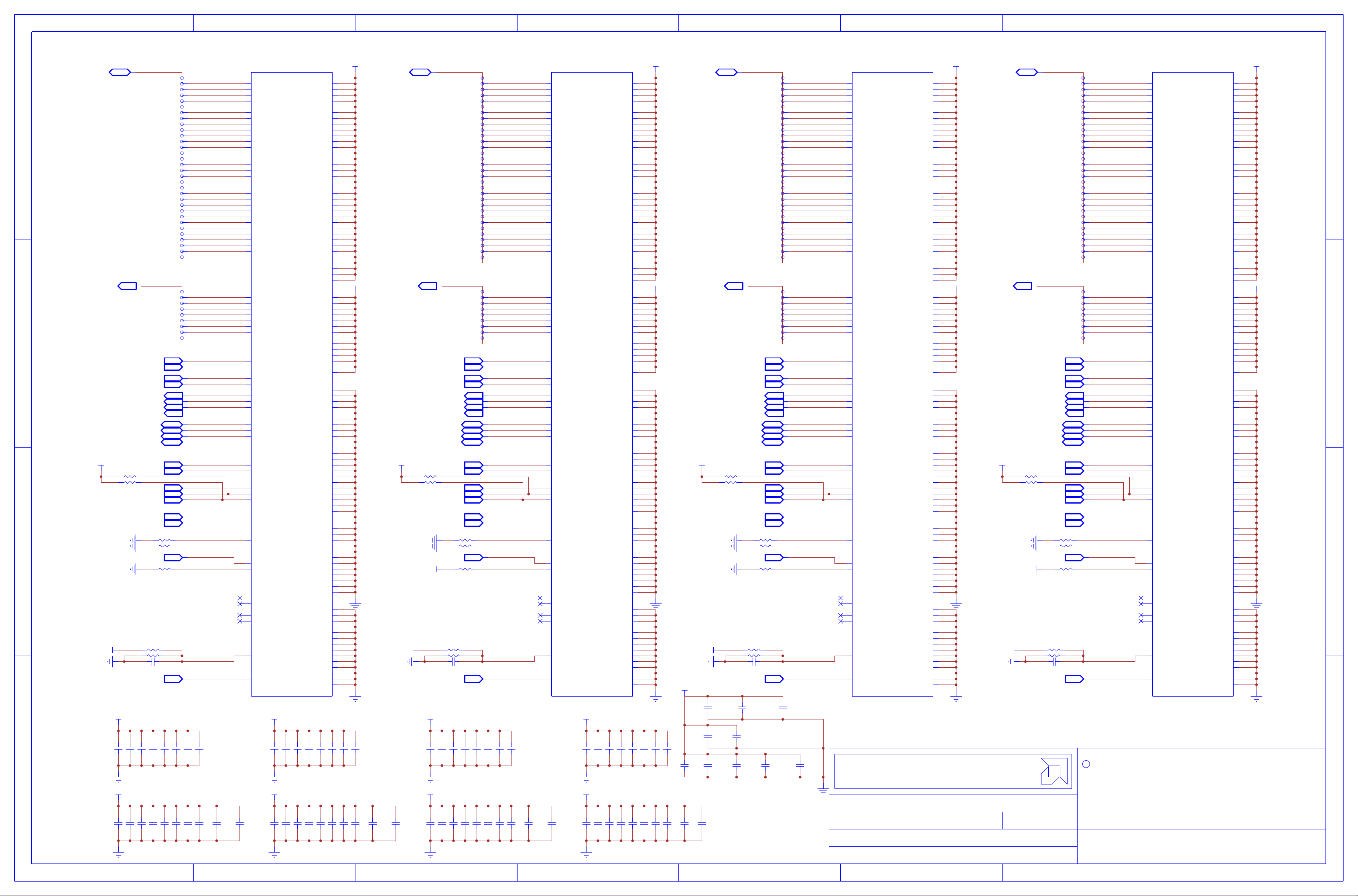
This AMD Board schematic and design is the exclusive property of AMD, and
DATE:
SHEET:
Advanced Micro Devices
2
3
345
6
6
7
7
8
8
C
5
CONFIDENTIAL AND PROPRIETARY TO ADVANCED MICRO DEVICES INC.
C
BB
A
1
DD
C
A
4
REV:
SHEET NUMBER:
DOCUMENT NUMBER:
OF
1
prohibited. Use of this schematic and design for any purpose other than
for evaluation purposes. Further distribution or disclosure is strictly
is provided only to entities under a non-disclosure agreement with AMD
2
schematic and design, including, not limited to, any implied warranty
AMD makes no representations or warranties of any kind regarding this
evaluation requires a Board Technology License Agreement with AMD.
of merchantability or fitness for a particular purpose, and disclaims
responsibility for any consequences resulting from use of the
information included herein.
TITLE:
INININININININININININININININININININININBIBIBIBI
OUT
OUT
OUT
OUTINININININININININBIBIBIBIOUT
OUT
OUT
OUTINININININININININBIBIBIBIOUT
OUT
OUT
OUTINININININININININBIBIBIBIOUT
OUT
OUT
OUTININININ
OUT
OUT
OUT
OUTBIBIBIBI
VSS_B5
VSS_B10
VSS_D10
VSS_G5
VSS_G10
VSS_H1
VSS_H14
VSS_K1
VSS_K14
VSS_L5
VSS_L10
VSS_P10
VSS_T5
VSS_T10
SEN
VSSQ_V14
VSSQ_V12
VSSQ_V3
VSSQ_V1
VSSQ_R14
VSSQ_R12
VSSQ_R11
VSSQ_R4
VSSQ_R3
VSSQ_R1
VSSQ_N1
VSSQ_N14
VSSQ_N12
VSSQ_N3
VSSQ_M10
VSSQ_M5
VSSQ_K13
VSSQ_K2
VSSQ_H13
VSSQ_H2
VSSQ_F10
VSSQ_F5
VSSQ_E14
VSSQ_E12
VSSQ_E3
VSSQ_E1
VSSQ_C14
VSSQ_C12
VSSQ_C11
VSSQ_C4
VSSQ_C3
VSSQ_C1
VSSQ_A14
VSSQ_A12
VSSQ_A3
VSSQ_A1
ZQ
VREFC
VDD_R10
VDD_R5
VDD_P11
VDD_L14
VDDQ_T14
VDDQ_T12
VDDQ_T3
VDDQ_T1
VDDQ_P14
VDDQ_P12
VDDQ_P3
VDDQ_P1
VDDQ_N10
VDDQ_N5
VDDQ_M14
VDDQ_M12
VDDQ_M3
VDDQ_M1
Vpp_NC1
Vpp_NC
WCK23#__WCK01#
WCK23__WCK01
WCK01#__WCK23#
WCK01__WCK23
RFU_A12_NC
VREFD2
VREFD1
MF
VDD_L11
VDD_L4
VDDQ_L13
VDDQ_L2
VDDQ_K12
VDDQ_K3
VDDQ_H12
VDDQ_H3
WE#__CS#
VDD_L1
VDD_G14
VDD_G11
VDD_G4
VDD_G1
VDD_D11
VDD_C10
VDD_C5
VDDQ_G13
VDDQ_G2
VDDQ_F14
VDDQ_F12
VDDQ_E10
DBI3#__DBI0#
DBI2#__DBI1#
DBI1#__DBI2#
DBI0#__DBI3#
EDC3__EDC0
EDC2__EDC1
EDC1__EDC2
EDC0__EDC3
VDDQ_E5
VDDQ_D14
VDDQ_D12
VDDQ_D3
VDDQ_D1
VDDQ_B14
VDDQ_B12
VDDQ_B3
VDDQ_B1
A5_BA1__A3_BA3
CK#
CK
VDDQ_F1
A1_A9__A6_A11
CKE#
RESET#
A2_BA0__A4_BA2
RAS#__CAS#
A6_A11__A1_A9
A7_A8__A0_A10
A4_BA2__A2_BA0
A0_A10__A7_A8
A3_BA3__A5_BA1
CS#__WE#
CAS#__RAS#
DQ0__DQ24
DQ1__DQ25
DQ2__DQ26
DQ3__DQ27
DQ4__DQ28
DQ5__DQ29
DQ6__DQ30
DQ7__DQ31
DQ8__DQ16
DQ9__DQ17
DQ10__DQ18
DQ11__DQ19
DQ12__DQ20
DQ13__DQ21
DQ14__DQ22
DQ15__DQ23
DQ16__DQ8
DQ17__DQ9
DQ18__DQ10
DQ19__DQ11
DQ20__DQ12
DQ21__DQ13
DQ22__DQ14
DQ23__DQ15
DQ24__DQ0
DQ25__DQ1
DQ26__DQ2
DQ27__DQ3
DQ28__DQ4
DQ29__DQ5
DQ30__DQ6
DQ31__DQ7
ABI#
VDDQ_F3
8
7
6
345
2
1
C
A
M2
M2
DQ31__DQ7
M4
M4
DQ30__DQ6
N2
N2
DQ29__DQ5
N4
N4
DQ28__DQ4
T2
T2
DQ27__DQ3
T4
T4
DQ26__DQ2
V2
V2
DQ25__DQ1
V4
V4
DQ24__DQ0
M13
M13
DQ23__DQ15
M11
M11
DQ22__DQ14
N13
N13
DQ21__DQ13
N11
N11
DQ20__DQ12
T13
T13
DQ19__DQ11
T11
T11
DQ18__DQ10
V13
V13
DQ17__DQ9
V11
V11
DQ16__DQ8
F13
F13
DQ15__DQ23
F11
F11
DQ14__DQ22
E13
E13
DQ13__DQ21
E11
E11
DQ12__DQ20
B13
B13
DQ11__DQ19
B11
B11
DQ10__DQ18
A13
A13
DQ9__DQ17
A11
A11
DQ8__DQ16
F2
F2
DQ7__DQ31
F4
F4
DQ6__DQ30
E2
E2
DQ5__DQ29
E4
E4
DQ4__DQ28
B2
B2
DQ3__DQ27
B4
B4
DQ2__DQ26
A2
A2
DQ1__DQ25
A4
A4
DQ0__DQ24
J5
J5
RFU_A12_NC
K4
K4
A7_A8__A0_A10
K5
K5
A6_A11__A1_A9
K10
K10
A5_BA1__A3_BA3
K11
K11
A4_BA2__A2_BA0
H10
H10
A3_BA3__A5_BA1
H11
H11
A2_BA0__A4_BA2
H5
H5
A1_A9__A6_A11
H4
H4
A0_A10__A7_A8
D4
D4
WCK01__WCK23
D5
D5
WCK01#__WCK23#
P4
P4
WCK23__WCK01
P5
P5
WCK23#__WCK01#
R2
R2
EDC3__EDC0
R13
R13
EDC2__EDC1
C13
C13
EDC1__EDC2
C2
C2
EDC0__EDC3
P2
P2
DBI3#__DBI0#
P13
P13
DBI2#__DBI1#
D13
D13
DBI1#__DBI2#
D2
D2
DBI0#__DBI3#
G3
G3
RAS#__CAS#
L3
L3
CAS#__RAS#
J3
J3
CKE#
J11
J11
CK#
J12
J12
CK
G12
G12
CS#__WE#
L12
L12
WE#__CS#
J13
J13
ZQ
J10
J10
SEN
J2
J2
RESET#
J1
J1
MF
A5
A5
Vpp_NC
V5
V5
Vpp_NC1
A10
A10
VREFD1
V10
V10
VREFD2
J14
J14
VREFC
J4
J4
ABI#
C2441
C2441
22uF
22uF
4V
4V
2 1
2 1
23CNOPN001
23CNOPN001
U2400
U2400
+MVDD
+MVDD
C2506
C2506
0.1uF
0.1uF
+MVDD +MVDD
+MVDD +MVDD
C2521
C2521
1uF
1uF
7
(6) GDDR5 MEMORY CH C/D
(6) GDDR5 MEMORY CH C/D
DQC0_<31..0>
DQC0_<31..0>
MAC0_<8..0>
MAC0_<8..0>
OUT OUT OUT OUT
4 6
4 6
4 6
4 6
4 6
4 6
4 6
4 6
4 6
4 6
4 6
4 6
4 6
4 6
4 6
4 6
4
4
IN
4
4
IN
4
4
IN
4
4
IN
4
4
OUT
4
4
OUT
4
4
OUT
4
4
OUT
4
4
BI
4
4
BI
4
4
BI
4
4
BI
4
4
IN
4
4
IN
1%60.4R
1%60.4R
1%60.4R
1%60.4R
4
4
IN
4
4
IN
4
4
IN
4
4
IN
4
4
IN
R2402
R2402
R2403
C2407
C2407
0.1uF
0.1uF
C2417
C2417
1uF
1uF
R2409
R2409
R2410
R2410
C2405
C2405
C2408
C2408
0.1uF
0.1uF
C2418
C2418
1uF
1uF
R2403
R2404
R2404
C2409
C2409
0.1uF
0.1uF
C2419
C2419
1uF
1uF
1K 5%
1K 5%
4 6
4 6
IN
6.3V
6.3V
1uF
1uF
4
4
IN IN
C2411
C2411
C2410
C2410
0.1uF
0.1uF
0.1uF
0.1uF
C2420
C2420
C2421
C2421
1uF
1uF
1uF
1uF
29
29
31
31
28
28
30
30
27
27
24
24
26
26
25
25
16
16
23
23
17
17
21
21
19
19
22
22
18
18
20
20
5
5
4
4
7
7
6
6
3
3
1
1
0
0
2
2
10
10
9
9
11
11
8
8
12
12
13
13
14
14
15
15
8
8
7
7
6
6
5
5
4
4
3
3
2
2
1
1
0
0
5%1K
5%1K
1%2.37K
1%2.37K
1%5.49K
1%5.49K
C2413
C2413
0.1uF
0.1uF
C2422
C2422
1uF
1uF
4 6
4 6
4 6
4 6
4 6
4 6
4 6
4 6
4 6
4 6
4 6
4 6
4 6
4 6
4 6
4 6
4 6
4 6
4 6
4 6
4 6
4 6
4 6
4 6
4 6
4 6
4 6
4 6
4 6
4 6
4 6
4 6
4 6
4 6
4 6
4 6
4 6
4 6
4 6
4 6
4 6
4 6
4 6
4 6
4 6
4 6
4 6
4 6
4 6
4 6
4 6
4 6
4 6
4 6
4 6
4 6
4 6
4 6
4 6
4 6
4 6
4 6
6
6
4
4
MAC0_<8>
MAC0_<8>
MAC0_<7>
MAC0_<7>
MAC0_<6>
MAC0_<6>
MAC0_<5>
MAC0_<5>
MAC0_<4>
MAC0_<4>
MAC0_<3>
MAC0_<3>
MAC0_<2>
MAC0_<2>
MAC0_<1>
MAC0_<1>
MAC0_<0>
MAC0_<0>
WCKC0_0
WCKC0_0
WCKC0b_0
WCKC0b_0
WCKC0_1
WCKC0_1
WCKC0b_1
WCKC0b_1
EDCC0_3
EDCC0_3
EDCC0_2
EDCC0_2
EDCC0_0
EDCC0_0
EDCC0_1
EDCC0_1
DDBIC0_3
DDBIC0_3
DDBIC0_2
DDBIC0_2
DDBIC0_0
DDBIC0_0
DDBIC0_1
DDBIC0_1
RASC0b
RASC0b
CASC0b
CASC0b
CKEC0
CKEC0
CLKC0b
CLKC0b
CLKC0
CLKC0
CSC0b_0
CSC0b_0
WEC0b
WEC0b
ZQ_C0
ZQ_C0
1%120R
1%120R
SEN_C0
SEN_C0
DRAM_RST2
DRAM_RST2
MF_C0
MF_C0
VREFC_C0
VREFC_C0
ADBIC0
ADBIC0
C2414
C2414
C2423
C2423
1uF 0.1uF
1uF 0.1uF
DQC0_<29>
DQC0_<29>
DQC0_<31>
DQC0_<31>
DQC0_<28>
DQC0_<28>
DQC0_<30>
DQC0_<30>
DQC0_<27>
DQC0_<27>
DQC0_<24>
DQC0_<24>
DQC0_<26>
DQC0_<26>
DQC0_<25>
DQC0_<25>
DQC0_<16>
DQC0_<16>
DQC0_<23>
DQC0_<23>
DQC0_<17>
DQC0_<17>
DQC0_<21>
DQC0_<21>
DQC0_<19>
DQC0_<19>
DQC0_<22>
DQC0_<22>
DQC0_<18>
DQC0_<18>
DQC0_<20>
DQC0_<20>
DQC0_<5>
DQC0_<5>
DQC0_<4>
DQC0_<4>
DQC0_<7>
DQC0_<7>
DQC0_<6>
DQC0_<6>
DQC0_<3>
DQC0_<3>
DQC0_<1>
DQC0_<1>
DQC0_<0>
DQC0_<0>
4 6
4 6
DQC0_<2>
DQC0_<2>
DQC0_<10>
DQC0_<10>
DQC0_<9>
DQC0_<9>
DQC0_<11>
DQC0_<11>
DQC0_<8>
DQC0_<8>
DQC0_<12>
DQC0_<12>
DQC0_<13>
DQC0_<13>
DQC0_<14>
DQC0_<14>
DQC0_<15>
DQC0_<15>
C2415
C2415
0.1uF
0.1uF
C2425
C2425
C2440
C2440
22uF
22uF
4V
4V
2 1
2 1
1uF
1uF
4 6 4 6
4 6 4 6
4 6
4 6
+MVDD
+MVDD
R2401
R2401
R2400
R2400
+MVDD
+MVDD
+MVDD
+MVDD
+MVDD
+MVDD
8
C2507
C2507
0.1uF
0.1uF
C2522
C2522
1uF
1uF
VDDQ_B1
VDDQ_B3
VDDQ_B12
VDDQ_B14
VDDQ_D1
VDDQ_D3
VDDQ_D12
VDDQ_D14
VDDQ_E5
VDDQ_E10
VDDQ_F1
VDDQ_F3
VDDQ_F12
VDDQ_F14
VDDQ_G2
VDDQ_G13
VDDQ_H3
VDDQ_H12
VDDQ_K3
VDDQ_K12
VDDQ_L2
VDDQ_L13
VDDQ_M1
VDDQ_M3
VDDQ_M12
VDDQ_M14
VDDQ_N5
VDDQ_N10
VDDQ_P1
VDDQ_P3
VDDQ_P12
VDDQ_P14
VDDQ_T1
VDDQ_T3
VDDQ_T12
VDDQ_T14
VDD_C5
VDD_C10
VDD_D11
VDD_G1
VDD_G4
VDD_G11
VDD_G14
VDD_L1
VDD_L4
VDD_L11
VDD_L14
VDD_P11
VDD_R5
VDD_R10
VSSQ_A1
VSSQ_A3
VSSQ_A12
VSSQ_A14
VSSQ_C1
VSSQ_C3
VSSQ_C4
VSSQ_C11
VSSQ_C12
VSSQ_C14
VSSQ_E1
VSSQ_E3
VSSQ_E12
VSSQ_E14
VSSQ_F5
VSSQ_F10
VSSQ_H2
VSSQ_H13
VSSQ_K2
VSSQ_K13
VSSQ_M5
VSSQ_M10
VSSQ_N1
VSSQ_N3
VSSQ_N12
VSSQ_N14
VSSQ_R1
VSSQ_R3
VSSQ_R4
VSSQ_R11
VSSQ_R12
VSSQ_R14
VSSQ_V1
VSSQ_V3
VSSQ_V12
VSSQ_V14
VSS_B5
VSS_B10
VSS_D10
VSS_G5
VSS_G10
VSS_H1
VSS_H14
VSS_K1
VSS_K14
VSS_L5
VSS_L10
VSS_P10
VSS_T5
VSS_T10
C2509
C2508
C2509
C2508
0.1uF
0.1uF
0.1uF
0.1uF
C2524
C2523
C2524
C2523
1uF
1uF
1uF
1uF
C2512
C2512
0.1uF
0.1uF
C2525
C2525
1uF
1uF
B1
B1
B3
B3
B12
B12
B14
B14
D1
D1
D3
D3
D12
D12
D14
D14
E5
E5
E10
E10
F1
F1
F3
F3
F12
F12
F14
F14
G2
G2
G13
G13
H3
H3
H12
H12
K3
K3
K12
K12
L2
L2
L13
L13
M1
M1
M3
M3
M12
M12
M14
M14
N5
N5
N10
N10
P1
P1
P3
P3
P12
P12
P14
P14
T1
T1
T3
T3
T12
T12
T14
T14
C5
C5
C10
C10
D11
D11
G1
G1
G4
G4
G11
G11
G14
G14
L1
L1
L4
L4
L11
L11
L14
L14
P11
P11
R5
R5
R10
R10
A1
A1
A3
A3
A12
A12
A14
A14
C1
C1
C3
C3
C4
C4
C11
C11
C12
C12
C14
C14
E1
E1
E3
E3
E12
E12
E14
E14
F5
F5
F10
F10
H2
H2
H13
H13
K2
K2
K13
K13
M5
M5
M10
M10
N1
N1
N3
N3
N12
N12
N14
N14
R1
R1
R3
R3
R4
R4
R11
R11
R12
R12
R14
R14
V1
V1
V3
V3
V12
V12
V14
V14
B5
B5
B10
B10
D10
D10
G5
G5
G10
G10
H1
H1
H14
H14
K1
K1
K14
K14
L5
L5
L10
L10
P10
P10
T5
T5
T10
T10
C2513
C2513
0.1uF
0.1uF
C2526
C2526
1uF
1uF
+MVDD
+MVDD
+MVDD
+MVDD
C2515
C2515
0.1uF
0.1uF
C2527
C2527
1uF
1uF
C2519
C2519
0.1uF
0.1uF
C2528
C2528
1uF
1uF
22uF
22uF
4V
4V
2 1
2 1
+MVDD
C2711
C2711
0.1uF
0.1uF
C2720
C2720
1uF
1uF
B1
B1
B3
B3
B12
B12
B14
B14
D1
D1
D3
D3
D12
D12
D14
D14
E5
E5
E10
E10
F1
F1
F3
F3
F12
F12
F14
F14
G2
G2
G13
G13
H3
H3
H12
H12
K3
K3
K12
K12
L2
L2
L13
L13
M1
M1
M3
M3
M12
M12
M14
M14
N5
N5
N10
N10
P1
P1
P3
P3
P12
P12
P14
P14
T1
T1
T3
T3
T12
T12
T14
T14
C5
C5
C10
C10
D11
D11
G1
G1
G4
G4
G11
G11
G14
G14
L1
L1
L4
L4
L11
L11
L14
L14
P11
P11
R5
R5
R10
R10
A1
A1
A3
A3
A12
A12
A14
A14
C1
C1
C3
C3
C4
C4
C11
C11
C12
C12
C14
C14
E1
E1
E3
E3
E12
E12
E14
E14
F5
F5
F10
F10
H2
H2
H13
H13
K2
K2
K13
K13
M5
M5
M10
M10
N1
N1
N3
N3
N12
N12
N14
N14
R1
R1
R3
R3
R4
R4
R11
R11
R12
R12
R14
R14
V1
V1
V3
V3
V12
V12
V14
V14
B5
B5
B10
B10
D10
D10
G5
G5
G10
G10
H1
H1
H14
H14
K1
K1
K14
K14
L5
L5
L10
L10
P10
P10
T5
T5
T10
T10
C2712
C2712
0.1uF
0.1uF
C2721
C2721
1uF
1uF
+MVDD
+MVDD
+MVDD
C2714
C2714
0.1uF
0.1uF
C2722
C2722
1uF
1uF
C2715
C2715
0.1uF
0.1uF
C2723
C2723
1uF
1uF
23CNOPN001
23CNOPN001
U2500
DQC1_<31..0>
DQC1_<31..0>
MAC1_<8..0> MAD1_<8..0>
4 6 4 6
4 6 4 6
+MVDD
+MVDD
R2501
R2501
R2500
R2500
+MVDD +MVDD
+MVDD +MVDD
C2540
C2541
C2540
C2541
22uF
22uF
4V 4V
4V 4V
2 1
2 1
MAC1_<8..0> MAD1_<8..0>
4
4
4
4
4
4
4
4
4
4
4
4
4
4
4
4
4
4
4
4
4
4
4
4
4
4
4
4
1%60.4R
1%60.4R
1%60.4R
1%60.4R
4
4
4
4
4
4
4
4
4
4
R2502
R2502
R2503
R2503
4 6
4 6
R2504
R2504
+MVDD +MVDD
+MVDD +MVDD
R2509
R2509
R2510
R2510
C2505
+MVDD
+MVDD
C2505
C2607
C2607
0.1uF
0.1uF
C2617
C2617
1uF
1uF
C2608
C2608
0.1uF
0.1uF
C2619
C2619
1uF
1uF
4
4
C2609
C2609
0.1uF
0.1uF
C2620
C2620
1uF
1uF
1uF
1uF
4 6
4 6
4 6
4 6
4 6
4 6
4 6
4 6
4 6
4 6
4 6
4 6
4 6
4 6
4 6
4 6
4 6
4 6
4 6
4 6
4 6
4 6
4 6
4 6
4 6
4 6
4 6
4 6
4 6
4 6
4 6
4 6
4 6
4 6
4 6
4 6
4 6
4 6
4 6
4 6
4 6
4 6
4 6
4 6
4 6
4 6
4 6
4 6
IN
IN
IN
IN
OUT
OUT
OUT
OUT
BI
BI
BI
BI
IN
IN
IN
IN
IN
IN
IN
IN
C2610
C2610
0.1uF
0.1uF
C2621
C2621
1uF
1uF
1%2.37K
1%2.37K
1%5.49K
1%5.49K
6.3V
6.3V
C2611
C2611
0.1uF
0.1uF
C2622
C2622
1uF
1uF
12
12
13
13
14
14
15
15
11
11
10
10
9
9
8
8
1
1
2
2
3
3
0
0
5
5
4
4
7
7
6
6
31
31
24
24
30
30
25
25
28
28
26
26
29
29
27
27
18
18
16
16
19
19
17
17
20
20
22
22
21
21
23
23
8
8
0
0
1
1
3
3
2
2
5
5
4
4
6
6
7
7
5%1K
5%1K
5%1K
5%1K
1%120R
1%120R
C2612
C2612
0.1uF
0.1uF
C2623
C2623
1uF
1uF
6
6
4
4
DQC1_<12>
4 6
4 6
DQC1_<12>
DQC1_<13>
4 6
4 6
DQC1_<13>
DQC1_<14>
4 6
DQC1_<14>
4 6
DQC1_<15>
4 6
DQC1_<15>
4 6
DQC1_<11>
4 6
DQC1_<11>
4 6
DQC1_<10>
4 6
4 6
DQC1_<10>
DQC1_<9>
4 6
4 6
DQC1_<9>
DQC1_<8>
4 6
4 6
DQC1_<8>
DQC1_<1>
4 6
4 6
DQC1_<1>
DQC1_<2>
4 6
DQC1_<2>
4 6
DQC1_<3>
4 6
4 6
DQC1_<3>
DQC1_<0>
4 6
4 6
DQC1_<0>
DQC1_<5>
4 6
4 6
DQC1_<5>
DQC1_<4>
4 6
4 6
DQC1_<4>
DQC1_<7>
4 6
4 6
DQC1_<7>
DQC1_<6>
4 6
4 6
DQC1_<6>
DQC1_<31>
DQC1_<31>
DQC1_<24>
DQC1_<24>
DQC1_<30>
DQC1_<30>
DQC1_<25>
DQC1_<25>
DQC1_<28>
DQC1_<28>
DQC1_<26>
DQC1_<26>
DQC1_<29>
DQC1_<29>
DQC1_<27>
DQC1_<27>
DQC1_<18>
DQC1_<18>
DQC1_<16>
DQC1_<16>
DQC1_<19>
DQC1_<19>
DQC1_<17>
DQC1_<17>
DQC1_<20>
DQC1_<20>
DQC1_<22>
DQC1_<22>
DQC1_<21>
DQC1_<21>
DQC1_<23>
DQC1_<23>
MAC1_<8>
MAC1_<8>
MAC1_<0>
MAC1_<0>
MAC1_<1>
MAC1_<1>
MAC1_<3>
MAC1_<3>
MAC1_<2>
MAC1_<2>
MAC1_<5>
MAC1_<5>
MAC1_<4>
MAC1_<4>
MAC1_<6>
MAC1_<6>
MAC1_<7>
MAC1_<7>
WCKC1_1
WCKC1_1
WCKC1b_1
WCKC1b_1
WCKC1_0
WCKC1_0
WCKC1b_0
WCKC1b_0
EDCC1_1
EDCC1_1
EDCC1_0
EDCC1_0
EDCC1_3
EDCC1_3
EDCC1_2
EDCC1_2
DDBIC1_1
DDBIC1_1
DDBIC1_0
DDBIC1_0
DDBIC1_3
DDBIC1_3
DDBIC1_2
DDBIC1_2
CASC1b
CASC1b
RASC1b
RASC1b
CKEC1
CKEC1
CLKC1b
CLKC1b
CLKC1
CLKC1
WEC1b
WEC1b
CSC1b_0
CSC1b_0
ZQ_C1
ZQ_C1
SEN_C1
SEN_C1
DRAM_RST2
DRAM_RST2
MF_C1
MF_C1
VREFC_C1
VREFC_C1
ADBIC1
ADBIC1
C2613
C2614
C2613
C2614
0.1uF
0.1uF
0.1uF
0.1uF
C2624
C2624
C2625
C2625
1uF
1uF
1uF
1uF
22uF
22uF
4V
4V
2 1
2 1
M2
M2
M4
M4
N2
N2
N4
N4
T2
T2
T4
T4
V2
V2
V4
V4
M13
M13
M11
M11
N13
N13
N11
N11
T13
T13
T11
T11
V13
V13
V11
V11
F13
F13
F11
F11
E13
E13
E11
E11
B13
B13
B11
B11
A13
A13
A11
A11
F2
F2
F4
F4
E2
E2
E4
E4
B2
B2
B4
B4
A2
A2
A4
A4
J5
J5
K4
K4
K5
K5
K10
K10
K11
K11
H10
H10
H11
H11
H5
H5
H4
H4
D4
D4
D5
D5
P4
P4
P5
P5
R2
R2
R13
R13
C13
C13
C2
C2
P2
P2
P13
P13
D13
D13
D2
D2
G3
G3
L3
L3
J3
J3
J11
J11
J12
J12
G12
G12
L12
L12
J13
J13
J10
J10
J2
J2
J1
J1
A5
A5
V5
V5
A10
A10
V10
V10
J14
J14
J4
J4
C2640
C2640
2 1
2 1
DQ31__DQ7
DQ30__DQ6
DQ29__DQ5
DQ28__DQ4
DQ27__DQ3
DQ26__DQ2
DQ25__DQ1
DQ24__DQ0
DQ23__DQ15
DQ22__DQ14
DQ21__DQ13
DQ20__DQ12
DQ19__DQ11
DQ18__DQ10
DQ17__DQ9
DQ16__DQ8
DQ15__DQ23
DQ14__DQ22
DQ13__DQ21
DQ12__DQ20
DQ11__DQ19
DQ10__DQ18
DQ9__DQ17
DQ8__DQ16
DQ7__DQ31
DQ6__DQ30
DQ5__DQ29
DQ4__DQ28
DQ3__DQ27
DQ2__DQ26
DQ1__DQ25
DQ0__DQ24
RFU_A12_NC
A7_A8__A0_A10
A6_A11__A1_A9
A5_BA1__A3_BA3
A4_BA2__A2_BA0
A3_BA3__A5_BA1
A2_BA0__A4_BA2
A1_A9__A6_A11
A0_A10__A7_A8
WCK01__WCK23
WCK01#__WCK23#
WCK23__WCK01
WCK23#__WCK01#
EDC3__EDC0
EDC2__EDC1
EDC1__EDC2
EDC0__EDC3
DBI3#__DBI0#
DBI2#__DBI1#
DBI1#__DBI2#
DBI0#__DBI3#
RAS#__CAS#
CAS#__RAS#
CKE#
CK#
CK
CS#__WE#
WE#__CS#
ZQ
SEN
RESET#
MF
Vpp_NC
Vpp_NC1
VREFD1
VREFD2
VREFC
ABI#
C2641
C2641
22uF
22uF
6
U2500 U2700
VDDQ_B1
VDDQ_B3
VDDQ_B12
VDDQ_B14
VDDQ_D1
VDDQ_D3
VDDQ_D12
VDDQ_D14
VDDQ_E5
VDDQ_E10
VDDQ_F1
VDDQ_F3
VDDQ_F12
VDDQ_F14
VDDQ_G2
VDDQ_G13
VDDQ_H3
VDDQ_H12
VDDQ_K3
VDDQ_K12
VDDQ_L2
VDDQ_L13
VDDQ_M1
VDDQ_M3
VDDQ_M12
VDDQ_M14
VDDQ_N5
VDDQ_N10
VDDQ_P1
VDDQ_P3
VDDQ_P12
VDDQ_P14
VDDQ_T1
VDDQ_T3
VDDQ_T12
VDDQ_T14
VDD_C5
VDD_C10
VDD_D11
VDD_G1
VDD_G4
VDD_G11
VDD_G14
VDD_L1
VDD_L4
VDD_L11
VDD_L14
VDD_P11
VDD_R5
VDD_R10
VSSQ_A1
VSSQ_A3
VSSQ_A12
VSSQ_A14
VSSQ_C1
VSSQ_C3
VSSQ_C4
VSSQ_C11
VSSQ_C12
VSSQ_C14
VSSQ_E1
VSSQ_E3
VSSQ_E12
VSSQ_E14
VSSQ_F5
VSSQ_F10
VSSQ_H2
VSSQ_H13
VSSQ_K2
VSSQ_K13
VSSQ_M5
VSSQ_M10
VSSQ_N1
VSSQ_N3
VSSQ_N12
VSSQ_N14
VSSQ_R1
VSSQ_R3
VSSQ_R4
VSSQ_R11
VSSQ_R12
VSSQ_R14
VSSQ_V1
VSSQ_V3
VSSQ_V12
VSSQ_V14
VSS_B5
VSS_B10
VSS_D10
VSS_G5
VSS_G10
VSS_H1
VSS_H14
VSS_K1
VSS_K14
VSS_L5
VSS_L10
VSS_P10
VSS_T5
VSS_T10
+MVDD
+MVDD
C2710
C2708
C2710
C2708
C2707
C2707
0.1uF
0.1uF
0.1uF
0.1uF
0.1uF
0.1uF
+MVDD
+MVDD
C2718
C2718
C2719
C2719
C2717
C2717
1uF
1uF
1uF
1uF
1uF
1uF
5
23CNOPN001
23CNOPN001
U2600
DQD0_<31..0>
4 6
4 6
DQD0_<31..0>
MAD0_<8..0>
MAD0_<8..0>
R2602
R2602
R2603
R2603
R2604
R2604
R2609
R2609
R2610
R2610
C2605
C2605
C2751
C2751
22uF
22uF
4V
4V
2 1
2 1
C2753C2752
C2753
10uF
10uF
4V
4V
2 1
2 1
C2761
10uF
10uF
2 1
2 1
6
6
4
DQD0_<13>
DQD0_<13>
4
13
13
4 6
4 6
4 6
4 6
4 6
4 6
4 6
4 6
4 6
4 6
4 6
4 6
4 6
4 6
4 6
4 6
4 6
4 6
4 6
4 6
4 6
4 6
4 6
4 6
4 6
4 6
4 6
4 6
4 6
4 6
4 6
4 6
4 6
4 6
4 6
4 6
4 6
4 6
4 6
4 6
4 6
4 6
4 6
4 6
4 6
4 6
4 6
4 6
4 6
4 6
4 6
4 6
4 6
4 6
4 6
4 6
4 6
4 6
4 6
4 6
4 6
4 6
4 6
4 6
4 6
4 6
4 6
4 6
4 6
4 6
4 6
4 6
4 6
4 6
4 6
4 6
4 6
4 6
4
4
IN
4
4
IN
4
4
IN
4
4
IN
4
4
OUT
4
4
OUT
4
4
OUT
4
4
OUT
4
4
BI
4
4
BI
4
4
BI
4
4
BI
4
4
IN
4
4
IN
1%60.4R
1%60.4R
1%60.4R
1%60.4R
4
4
IN
4
4
IN
4
4
IN
4
4
IN
4
4
IN
4 6
4 6
IN
1uF
1uF
4
4
IN IN
C2762C2761C2760
C2762
10uF 10uF
10uF 10uF
2 1
2 1
1%2.37K
1%2.37K
1%5.49K
1%5.49K
6.3V
6.3V
2 1
2 1
15
15
12
12
14
14
10
10
8
8
11
11
9
9
0
0
7
7
2
2
6
6
3
3
5
5
1
1
4
4
20
20
23
23
21
21
22
22
19
19
18
18
17
17
16
16
26
26
25
25
27
27
24
24
28
28
29
29
30
30
31
31
8
8
7
7
6
6
5
5
4
4
3
3
2
2
1
1
0
0
1%120R
1%120R
5%1K
5%1K
5%1K
5%1K
C2755
C2755
22uF
22uF
4V
4V
DQD0_<15>
DQD0_<15>
DQD0_<12>
DQD0_<12>
DQD0_<14>
DQD0_<14>
DQD0_<10>
DQD0_<10>
DQD0_<8>
DQD0_<8>
DQD0_<11>
DQD0_<11>
DQD0_<9>
DQD0_<9>
DQD0_<0>
DQD0_<0>
DQD0_<7>
DQD0_<7>
DQD0_<2>
DQD0_<2>
DQD0_<6>
DQD0_<6>
DQD0_<3>
DQD0_<3>
DQD0_<5>
DQD0_<5>
DQD0_<1>
DQD0_<1>
DQD0_<4>
DQD0_<4>
DQD0_<20>
DQD0_<20>
DQD0_<23>
DQD0_<23>
DQD0_<21>
DQD0_<21>
DQD0_<22>
DQD0_<22>
DQD0_<19>
DQD0_<19>
DQD0_<18>
DQD0_<18>
DQD0_<17>
DQD0_<17>
DQD0_<16>
DQD0_<16>
DQD0_<26>
DQD0_<26>
DQD0_<25>
DQD0_<25>
DQD0_<27>
DQD0_<27>
DQD0_<24>
DQD0_<24>
DQD0_<28>
DQD0_<28>
DQD0_<29>
DQD0_<29>
DQD0_<30>
DQD0_<30>
DQD0_<31>
DQD0_<31>
6
6
4
4
MAD0_<8>
MAD0_<8>
MAD0_<7>
MAD0_<7>
MAD0_<6>
MAD0_<6>
MAD0_<5>
MAD0_<5>
MAD0_<4>
MAD0_<4>
MAD0_<3>
MAD0_<3>
MAD0_<2>
MAD0_<2>
MAD0_<1>
MAD0_<1>
MAD0_<0>
MAD0_<0>
WCKD0_1
WCKD0_1
WCKD0b_1
WCKD0b_1
WCKD0_0
WCKD0_0
WCKD0b_0
WCKD0b_0
EDCD0_1
EDCD0_1
EDCD0_0
EDCD0_0
EDCD0_2
EDCD0_2
EDCD0_3
EDCD0_3
DDBID0_1
DDBID0_1
DDBID0_0
DDBID0_0
DDBID0_2
DDBID0_2
DDBID0_3
DDBID0_3
RASD0b
RASD0b
CASD0b
CASD0b
CKED0
CKED0
CLKD0b
CLKD0b
CLKD0
CLKD0
CSD0b_0
CSD0b_0
WED0b
WED0b
ZQ_D0
ZQ_D0
SEN_D0
SEN_D0
DRAM_RST2
DRAM_RST2
MF_D0
MF_D0
VREFC_D0
VREFC_D0
ADBID0
ADBID0
C2763
C2763
4V
4V
2 1
2 1
M2
M2
DQ31__DQ7
M4
M4
DQ30__DQ6
N2
N2
DQ29__DQ5
N4
N4
DQ28__DQ4
T2
T2
DQ27__DQ3
T4
T4
DQ26__DQ2
V2
V2
DQ25__DQ1
V4
V4
DQ24__DQ0
M13
M13
DQ23__DQ15
M11
M11
DQ22__DQ14
N13
N13
DQ21__DQ13
N11
N11
DQ20__DQ12
T13
T13
DQ19__DQ11
T11
T11
DQ18__DQ10
V13
V13
DQ17__DQ9
V11
V11
DQ16__DQ8
F13
F13
DQ15__DQ23
F11
F11
DQ14__DQ22
E13
E13
DQ13__DQ21
E11
E11
DQ12__DQ20
B13
B13
DQ11__DQ19
B11
B11
DQ10__DQ18
A13
A13
DQ9__DQ17
A11
A11
DQ8__DQ16
F2
F2
DQ7__DQ31
F4
F4
DQ6__DQ30
E2
E2
DQ5__DQ29
E4
E4
DQ4__DQ28
B2
B2
DQ3__DQ27
B4
B4
DQ2__DQ26
A2
A2
DQ1__DQ25
A4
A4
DQ0__DQ24
J5
J5
RFU_A12_NC
K4
K4
A7_A8__A0_A10
K5
K5
A6_A11__A1_A9
K10
K10
A5_BA1__A3_BA3
K11
K11
A4_BA2__A2_BA0
H10
H10
A3_BA3__A5_BA1
H11
H11
A2_BA0__A4_BA2
H5
H5
A1_A9__A6_A11
H4
H4
A0_A10__A7_A8
D4
D4
WCK01__WCK23
D5
D5
WCK01#__WCK23#
P4
P4
WCK23__WCK01
P5
P5
WCK23#__WCK01#
R2
R2
EDC3__EDC0
R13
R13
EDC2__EDC1
C13
C13
EDC1__EDC2
C2
C2
EDC0__EDC3
P2
P2
DBI3#__DBI0#
P13
P13
DBI2#__DBI1#
D13
D13
DBI1#__DBI2#
D2
D2
DBI0#__DBI3#
G3
G3
RAS#__CAS#
L3
L3
CAS#__RAS#
J3
J3
CKE#
J11
J11
CK#
J12
J12
CK
G12
G12
CS#__WE#
L12
L12
WE#__CS#
J13
J13
ZQ
J10
J10
SEN
J2
J2
RESET#
J1
J1
MF
A5
A5
Vpp_NC
V5
V5
Vpp_NC1
A10
A10
VREFD1
V10
V10
VREFD2
J14
J14
VREFC
J4
J4
ABI#
AMD - PLATFORM HARDWARE ENG
AMD - PLATFORM HARDWARE ENG
#48, No.1387, ZHANGDONG ROAD
#48, No.1387, ZHANGDONG ROAD
SHANGHAI, CHINA 201203
SHANGHAI, CHINA 201203
4 6
4 6
+MVDD +MVDD
+MVDD +MVDD
R2601
R2601
R2600
R2600
+MVDD
+MVDD
C2750
C2750
22uF
22uF
4V
4V
2 1
2 1
C2752
10uF
10uF
4V
C2716
C2716
0.1uF
0.1uF
2 1
2 1
4V
2 1
2 1
C2764
C2764
C2760
10uF
10uF
10uF
10uF
4V 4V4V
4V
4V 4V4V
4V
2 1
2 1
Reserved. detail please check BOM
Reserved. detail please check BOM
SHEET:
C2740
C2740
22uF
22uF
4V
4V
22uF
22uF
4V
4V
2 1
2 1
C2741
C2741
DATE:
SHEET NUMBER:
DOCUMENT NUMBER:
4
C2724
C2724
1uF
1uF
2 1
2 1
U2600
VDDQ_B1
VDDQ_B3
VDDQ_B12
VDDQ_B14
VDDQ_D1
VDDQ_D3
VDDQ_D12
VDDQ_D14
VDDQ_E5
VDDQ_E10
VDDQ_F1
VDDQ_F3
VDDQ_F12
VDDQ_F14
VDDQ_G2
VDDQ_G13
VDDQ_H3
VDDQ_H12
VDDQ_K3
VDDQ_K12
VDDQ_L2
VDDQ_L13
VDDQ_M1
VDDQ_M3
VDDQ_M12
VDDQ_M14
VDDQ_N5
VDDQ_N10
VDDQ_P1
VDDQ_P3
VDDQ_P12
VDDQ_P14
VDDQ_T1
VDDQ_T3
VDDQ_T12
VDDQ_T14
VDD_C5
VDD_C10
VDD_D11
VDD_G1
VDD_G4
VDD_G11
VDD_G14
VDD_L1
VDD_L4
VDD_L11
VDD_L14
VDD_P11
VDD_R5
VDD_R10
VSSQ_A1
VSSQ_A3
VSSQ_A12
VSSQ_A14
VSSQ_C1
VSSQ_C3
VSSQ_C4
VSSQ_C11
VSSQ_C12
VSSQ_C14
VSSQ_E1
VSSQ_E3
VSSQ_E12
VSSQ_E14
VSSQ_F5
VSSQ_F10
VSSQ_H2
VSSQ_H13
VSSQ_K2
VSSQ_K13
VSSQ_M5
VSSQ_M10
VSSQ_N1
VSSQ_N3
VSSQ_N12
VSSQ_N14
VSSQ_R1
VSSQ_R3
VSSQ_R4
VSSQ_R11
VSSQ_R12
VSSQ_R14
VSSQ_V1
VSSQ_V3
VSSQ_V12
VSSQ_V14
VSS_B5
VSS_B10
VSS_D10
VSS_G5
VSS_G10
VSS_H1
VSS_H14
VSS_K1
VSS_K14
VSS_L5
VSS_L10
VSS_P10
VSS_T5
VSS_T10
GDDR5 MEM CH CD
GDDR5 MEM CH CD
Wed Apr 13 17:02:17 2016 1.0
Wed Apr 13 17:02:17 2016 1.0
6 26
6 26
B1
B1
B3
B3
B12
B12
B14
B14
D1
D1
D3
D3
D12
D12
D14
D14
E5
E5
E10
E10
F1
F1
F3
F3
F12
F12
F14
F14
G2
G2
G13
G13
H3
H3
H12
H12
K3
K3
K12
K12
L2
L2
L13
L13
M1
M1
M3
M3
M12
M12
M14
M14
N5
N5
N10
N10
P1
P1
P3
P3
P12
P12
P14
P14
T1
T1
T3
T3
T12
T12
T14
T14
+MVDD
+MVDD
C5
C5
C10
C10
D11
D11
G1
G1
G4
G4
G11
G11
G14
G14
L1
L1
L4
L4
L11
L11
L14
L14
P11
P11
R5
R5
R10
R10
A1
A1
A3
A3
A12
A12
A14
A14
C1
C1
C3
C3
C4
C4
C11
C11
C12
C12
C14
C14
E1
E1
E3
E3
E12
E12
E14
E14
F5
F5
F10
F10
H2
H2
H13
H13
K2
K2
K13
K13
M5
M5
M10
M10
N1
N1
N3
N3
N12
N12
N14
N14
R1
R1
R3
R3
R4
R4
R11
R11
R12
R12
R14
R14
V1
V1
V3
V3
V12
V12
V14
V14
B5
B5
B10
B10
D10
D10
G5
G5
G10
G10
H1
H1
H14
H14
K1
K1
K14
K14
L5
L5
L10
L10
P10
P10
T5
T5
T10
T10
OF
105_D009XX_00
105_D009XX_00
3
+MVDD
+MVDD
4 6
4 6
R2701
R2701
R2700
R2700
REV:
BIBIBIBI
DQD1_<31..0>
DQD1_<31..0>
R2702
R2702
R2703
R2703
R2704
R2704
R2709
R2709
R2710
R2710
C2705
C2705
VDDQ_B1
VDDQ_B3
VDDQ_B12
VDDQ_B14
VDDQ_D1
VDDQ_D3
VDDQ_D12
VDDQ_D14
VDDQ_E5
VDDQ_E10
VDDQ_F1
VDDQ_F3
VDDQ_F12
VDDQ_F14
VDDQ_G2
VDDQ_G13
VDDQ_H3
VDDQ_H12
VDDQ_K3
VDDQ_K12
VDDQ_L2
VDDQ_L13
VDDQ_M1
VDDQ_M3
VDDQ_M12
VDDQ_M14
VDDQ_N5
VDDQ_N10
VDDQ_P1
VDDQ_P3
VDDQ_P12
VDDQ_P14
VDDQ_T1
VDDQ_T3
VDDQ_T12
VDDQ_T14
VDD_C5
VDD_C10
VDD_D11
VDD_G1
VDD_G4
VDD_G11
VDD_G14
VDD_L1
VDD_L4
VDD_L11
VDD_L14
VDD_P11
VDD_R5
VDD_R10
VSSQ_A1
VSSQ_A3
VSSQ_A12
VSSQ_A14
VSSQ_C1
VSSQ_C3
VSSQ_C4
VSSQ_C11
VSSQ_C12
VSSQ_C14
VSSQ_E1
VSSQ_E3
VSSQ_E12
VSSQ_E14
VSSQ_F5
VSSQ_F10
VSSQ_H2
VSSQ_H13
VSSQ_K2
VSSQ_K13
VSSQ_M5
VSSQ_M10
VSSQ_N1
VSSQ_N3
VSSQ_N12
VSSQ_N14
VSSQ_R1
VSSQ_R3
VSSQ_R4
VSSQ_R11
VSSQ_R12
VSSQ_R14
VSSQ_V1
VSSQ_V3
VSSQ_V12
VSSQ_V14
VSS_B5
VSS_B10
VSS_D10
VSS_G5
VSS_G10
VSS_H1
VSS_H14
VSS_K1
VSS_K14
VSS_L5
VSS_L10
VSS_P10
VSS_T5
VSS_T10
23CNOPN001
23CNOPN001
DQD1_<20>
4 6
4 6
DQD1_<20>
20
20
DQD1_<21>
4 6
4 6
DQD1_<21>
21
21
DQD1_<23>
4 6
4 6
DQD1_<23>
23
23
DQD1_<22>
4 6
4 6
DQD1_<22>
22
22
DQD1_<19>
4 6
4 6
DQD1_<19>
19
19
DQD1_<18>
4 6
4 6
DQD1_<18>
18
18
DQD1_<16>
4 6
4 6
DQD1_<16>
16
16
4 6
4 6
DQD1_<17>
DQD1_<17>
17
17
DQD1_<26>
4 6
4 6
DQD1_<26>
26
26
DQD1_<25>
4 6
4 6
DQD1_<25>
25
25
DQD1_<27>
4 6
4 6
DQD1_<27>
27
27
DQD1_<24>
4 6
4 6
DQD1_<24>
24
24
DQD1_<28>
4 6
4 6
DQD1_<28>
28
28
DQD1_<29>
4 6
4 6
DQD1_<29>
29
29
DQD1_<30>
4 6
4 6
DQD1_<30>
30
30
DQD1_<31>
4 6
4 6
DQD1_<31>
31
31
DQD1_<14>
4 6
4 6
DQD1_<14>
14
14
DQD1_<8>
4 6
4 6
DQD1_<8>
8
8
DQD1_<15>
4 6
4 6
DQD1_<15>
15
15
DQD1_<9>
4 6
4 6
DQD1_<9>
9
9
DQD1_<13>
4 6
4 6
DQD1_<13>
13
13
DQD1_<10>
4 6
4 6
DQD1_<10>
10
10
DQD1_<12>
4 6
4 6
DQD1_<12>
12
12
4 6
4 6
DQD1_<11>
DQD1_<11>
11
11
4 6
4 6
DQD1_<3>
DQD1_<3>
3
3
4 6
DQD1_<0>
4 6
DQD1_<0>
0
0
DQD1_<2>
4 6
4 6
DQD1_<2>
2
2
4 6
4 6
DQD1_<1>
DQD1_<1>
1
1
DQD1_<4>
4 6
4 6
DQD1_<4>
4
4
4 6
4 6
DQD1_<5>
DQD1_<5>
5
5
4 6
4 6
DQD1_<7>
DQD1_<7>
7
7
4 6
4 6
DQD1_<6>
DQD1_<6>
6
6
6
6
4
4
MAD1_<8>
MAD1_<8>
8
8
4 6
4 6
4 6
4 6
4 6
4 6
4 6
4 6
4 6
4 6
4 6
4 6
4 6
4 6
4 6
4 6
4
4
IN
4
4
IN
4
4
IN
4
4
IN
4
4
OUT
4
4
OUT
4
4
OUT
4
4
OUT
4
4
BI
4
4
BI
4
4
BI
4
4
BI
4
4
IN
4
4
IN
1%60.4R
1%60.4R
1%60.4R
1%60.4R
4
4
IN
4
4
IN
4
4
IN
4
4
IN
4
4
IN
4 6
4 6
IN
1uF
1uF
4
4
MAD1_<0>
MAD1_<0>
0
0
MAD1_<1>
MAD1_<1>
1
1
MAD1_<3>
MAD1_<3>
3
3
MAD1_<2>
MAD1_<2>
2
2
MAD1_<5>
MAD1_<5>
5
5
MAD1_<4>
MAD1_<4>
4
4
MAD1_<6>
MAD1_<6>
6
6
MAD1_<7>
MAD1_<7>
7
7
WCKD1_0
WCKD1_0
WCKD1b_0
WCKD1b_0
WCKD1_1
WCKD1_1
WCKD1b_1
WCKD1b_1
EDCD1_2
EDCD1_2
EDCD1_3
EDCD1_3
EDCD1_1
EDCD1_1
EDCD1_0
EDCD1_0
DDBID1_2
DDBID1_2
DDBID1_3
DDBID1_3
DDBID1_1
DDBID1_1
DDBID1_0
DDBID1_0
CASD1b
CASD1b
RASD1b
RASD1b
CKED1
CKED1
CLKD1b
CLKD1b
CLKD1
CLKD1
WED1b
WED1b
CSD1b_0
CSD1b_0
1%120R
1%120R
ZQ_D1
ZQ_D1
SEN_D1
5%1K
5%1K
SEN_D1
DRAM_RST2
DRAM_RST2
MF_D1
5%1K
5%1K
MF_D1
1%2.37K
1%2.37K
1%5.49K
1%5.49K
VREFC_D1
6.3V
6.3V
VREFC_D1
ADBID1
ADBID1
CONFIDENTIAL AND PROPRIETARY TO ADVANCED MICRO DEVICES INC.
2016
2016
C
This AMD Board schematic and design is the exclusive property of AMD, and
is provided only to entities under a non-disclosure agreement with AMD
for evaluation purposes. Further distribution or disclosure is strictly
prohibited. Use of this schematic and design for any purpose other than
evaluation requires a Board Technology License Agreement with AMD.
AMD makes no representations or warranties of any kind regarding this
schematic and design, including, not limited to, any implied warranty
of merchantability or fitness for a particular purpose, and disclaims
responsibility for any consequences resulting from use of the
information included herein.
TITLE:
M2
M2
DQ31__DQ7
M4
M4
DQ30__DQ6
N2
N2
DQ29__DQ5
N4
N4
DQ28__DQ4
T2
T2
DQ27__DQ3
T4
T4
DQ26__DQ2
V2
V2
DQ25__DQ1
V4
V4
DQ24__DQ0
M13
M13
DQ23__DQ15
M11
M11
DQ22__DQ14
N13
N13
DQ21__DQ13
N11
N11
DQ20__DQ12
T13
T13
DQ19__DQ11
T11
T11
DQ18__DQ10
V13
V13
DQ17__DQ9
V11
V11
DQ16__DQ8
F13
F13
DQ15__DQ23
F11
F11
DQ14__DQ22
E13
E13
DQ13__DQ21
E11
E11
DQ12__DQ20
B13
B13
DQ11__DQ19
B11
B11
DQ10__DQ18
A13
A13
DQ9__DQ17
A11
A11
DQ8__DQ16
F2
F2
DQ7__DQ31
F4
F4
DQ6__DQ30
E2
E2
DQ5__DQ29
E4
E4
DQ4__DQ28
B2
B2
DQ3__DQ27
B4
B4
DQ2__DQ26
A2
A2
DQ1__DQ25
A4
A4
DQ0__DQ24
J5
J5
RFU_A12_NC
K4
K4
A7_A8__A0_A10
K5
K5
A6_A11__A1_A9
K10
K10
A5_BA1__A3_BA3
K11
K11
A4_BA2__A2_BA0
H10
H10
A3_BA3__A5_BA1
H11
H11
A2_BA0__A4_BA2
H5
H5
A1_A9__A6_A11
H4
H4
A0_A10__A7_A8
D4
D4
WCK01__WCK23
D5
D5
WCK01#__WCK23#
P4
P4
WCK23__WCK01
P5
P5
WCK23#__WCK01#
R2
R2
EDC3__EDC0
R13
R13
EDC2__EDC1
C13
C13
EDC1__EDC2
C2
C2
EDC0__EDC3
P2
P2
DBI3#__DBI0#
P13
P13
DBI2#__DBI1#
D13
D13
DBI1#__DBI2#
D2
D2
DBI0#__DBI3#
G3
G3
RAS#__CAS#
L3
L3
CAS#__RAS#
J3
J3
CKE#
J11
J11
CK#
J12
J12
CK
G12
G12
CS#__WE#
L12
L12
WE#__CS#
J13
J13
ZQ
J10
J10
SEN
J2
J2
RESET#
J1
J1
MF
A5
A5
Vpp_NC
V5
V5
Vpp_NC1
A10
A10
VREFD1
V10
V10
VREFD2
J14
J14
VREFC
J4
J4
ABI#
Advanced Micro Devices
Ellesmere XT/PRO GD5 8L
Ellesmere XT/PRO GD5 8L
U2700
2
B1
B1
B3
B3
B12
B12
B14
B14
D1
D1
D3
D3
D12
D12
D14
D14
E5
E5
E10
E10
F1
F1
F3
F3
F12
F12
F14
F14
G2
G2
G13
G13
H3
H3
H12
H12
K3
K3
K12
K12
L2
L2
L13
L13
M1
M1
M3
M3
M12
M12
M14
M14
N5
N5
N10
N10
P1
P1
P3
P3
P12
P12
P14
P14
T1
T1
T3
T3
T12
T12
T14
T14
C5
C5
C10
C10
D11
D11
G1
G1
G4
G4
G11
G11
G14
G14
L1
L1
L4
L4
L11
L11
L14
L14
P11
P11
R5
R5
R10
R10
A1
A1
A3
A3
A12
A12
A14
A14
C1
C1
C3
C3
C4
C4
C11
C11
C12
C12
C14
C14
E1
E1
E3
E3
E12
E12
E14
E14
F5
F5
F10
F10
H2
H2
H13
H13
K2
K2
K13
K13
M5
M5
M10
M10
N1
N1
N3
N3
N12
N12
N14
N14
R1
R1
R3
R3
R4
R4
R11
R11
R12
R12
R14
R14
V1
V1
V3
V3
V12
V12
V14
V14
B5
B5
B10
B10
D10
D10
G5
G5
G10
G10
H1
H1
H14
H14
K1
K1
K14
K14
L5
L5
L10
L10
P10
P10
T5
T5
T10
T10
1
+MVDD+MVDD
+MVDD+MVDD
+MVDD
+MVDD
DD
C
BB
A
Page 7

This AMD Board schematic and design is the exclusive property of AMD, and
DATE:
SHEET:
Advanced Micro Devices
2
3
345
6
6
7
7
8
8
C
5
CONFIDENTIAL AND PROPRIETARY TO ADVANCED MICRO DEVICES INC.
C
BB
A
1
DD
C
A
4
REV:
SHEET NUMBER:
DOCUMENT NUMBER:
OF
1
prohibited. Use of this schematic and design for any purpose other than
for evaluation purposes. Further distribution or disclosure is strictly
is provided only to entities under a non-disclosure agreement with AMD
2
schematic and design, including, not limited to, any implied warranty
AMD makes no representations or warranties of any kind regarding this
evaluation requires a Board Technology License Agreement with AMD.
of merchantability or fitness for a particular purpose, and disclaims
responsibility for any consequences resulting from use of the
information included herein.
TITLE:
IN
OUT
SSON
XIN CLKOUT1
VSSXOUT
VDD
IN
OUTINOUTININ
OUT
IN
SI
SCK
HOLD
VDD
GND
WP
SO
CE
OUT
REV 0.90
L
P
L
L
A
X
S
T
PART 9 OF 18
ANALOGIO
PLLCHARZ_L
PLLCHARZ_H
XTALOUT
XTALIN
REV 0.90
PART 8 OF 18
P
V
D
DBGDATA_15
DBGDATA_14
DBGDATA_13
DBGDATA_12
DBGDATA_11
DBGDATA_10
DBGDATA_9
DBGDATA_8
DBGDATA_5
DBGDATA_4
DBGDATA_3
DBGDATA_2
DBGDATA_1
DBGDATA_0
DBGDATA_7
DBGDATA_6
SWAPLOCKB
GENLK_VSYNC
GENLK_CLK
SWAPLOCKA
REV 0.90
G
P
I
O
PART 7 OF 18
VDD_33
VDD_33
VSYNC
HSYNC
TEST_PG_BACO
DIGON
WAKEB
BL_ENABLE
BL_PWM_DIM
GPIO_15
GPIO_5_REG_HOT_AC_BATT
GPIO_20
GPIO_16_8P_DETECT
GPIO_11
GPIO_12
GPIO_13
GPIO_14_HPD2
HPD1
GENERICG_HPD6
GENERICF_HPD5
GENERICE_HPD4
GENERICD
GENERICC
GENERICB
GENERICA
GPIO_30
GPIO_29
CLKREQB
TEST_PG
GPIO_17_THERMAL_INT
GPIO_22_ROMCSB
GPIO_1
GPIO_0
GPIO_2
GPIO_6_TACH
GPIO_8_ROMSO
GPIO_9_ROMSI
GPIO_10_ROMSCK
GPIO_18_HPD3
GPIO_19_CTF
GPIO_21
ININININOUT
OUT
IN
8
7
6
345
2
1
(7) ELLESMERE GPIO STRAP CF XTAL
(7) ELLESMERE GPIO STRAP CF XTAL
+VDDC
+VDDC
+0.8V
+0.8V
C
A
SCL/SDA BUS:
SCL/SDA BUS:
I2C ADDRESS
I2C ADDRESS
DDCVGA BUS:
DDCVGA BUS:
I2C ADDRESS
I2C ADDRESS
0x98
0x98
+MVDD
+MVDD
R66
R66
MR66
19 21
19 21
IN
0.8V_PGOOD
0.8V_PGOOD
R67
R67
MR67
MR67
FUNCTION
FUNCTION
EXT TEMP SENSOR LM96063
EXT TEMP SENSOR LM96063
5.1K
5.1K
21
21
21MR66
21
5.1K
5.1K
5%20K
5%20K
5%
5%
21
21
1K
1K
R62
R62
1K
1K
5%
5%
2 1
2 1
8
FUNCTION
FUNCTION
5%
5
5
5%
5%
5%
C69
C69
1uF
1uF
6.3V
6.3V
2 1
2 1
5
5
C68
1uF
1uF
6.3V
6.3V
2 1
2 1
+3.3V_BUS
+3.3V_BUS
R79
R79
10K
10K
5%
5%
2 1
2 14 3
Q31
Q31
MMDT3904-7
MMDT3904-7
4 3
+3.3V_BUS
+3.3V_BUS
R68
R68
10K
10K
5%
5%
2 14 3
2 1
Q30
Q30
MMDT3904-7
MMDT3904-7
4 3
GENLK_VSYNC
GENLK_VSYNC
7
7
DEVICE
DEVICE
DEVICE
DEVICE
+3.3V_BUS
+3.3V_BUS
C18
C1
C18
C1
1uF
1uF
1uF
1uF
6.3V
6.3V
6.3V
2 1
2 1
+1.8V
+1.8V
R89
R89
1K
1K
5%
5%
2 11 6
2 1
PG
PG
2
2
2
2
1 6
+1.8V
+1.8V
2 1
2 1
1 6
1 6
AT25
AT25
AR25
AR25
AM27
AM27
AL27
AL27
Q31
Q31
MMDT3904-7
MMDT3904-7
R69
R69
1K
1K
5%
5%
PG_BACO
PG_BACO
Q30
Q30C68
MMDT3904-7
MMDT3904-7
SWAPLOCKA
SWAPLOCKB
GENLK_CLK
GENLK_VSYNC
MR89
MR89
1K
1K
5%
5%
2 1
MR69
MR69
1K
1K
5%
5%
2 1
2 1 2 1
U1
U1
PART 8 OF 18
D
V
P
ellesmere_l4
ellesmere_l4
DBGDATA_0
DBGDATA_1
DBGDATA_2
DBGDATA_3
DBGDATA_4
DBGDATA_5
DBGDATA_6
DBGDATA_7
DBGDATA_8
DBGDATA_9
DBGDATA_10
DBGDATA_11
DBGDATA_12
DBGDATA_13
DBGDATA_14
DBGDATA_15
REV 0.90
AV18
AV18
AW18
AW18
AT19
AT19
AV19
AV19
AW19
AW19
AR20
AR20
AT20
AT20
AY20
AY20
AW20
AW20
AU20
AU20
AN21
AN21
AP21
AP21
AW21
AW21
AV21
AV21
AU21
AU21
AR21
AR21
6.3V
DVPDATA_0
DVPDATA_0
DVPDATA_1
DVPDATA_1
DVPDATA_2
DVPDATA_2
DVPDATA_3
DVPDATA_3
DVPDATA_4
DVPDATA_4
DVPDATA_5
DVPDATA_5
DVPDATA_6
DVPDATA_6
DVPDATA_7
DVPDATA_7
7
7
DVPDATA_8
DVPDATA_8
DVPDATA_9
DVPDATA_9
DVPDATA_10
DVPDATA_10
DVPDATA_11
DVPDATA_11
DVPDATA_12
DVPDATA_12
DVPDATA_13
DVPDATA_13
DVPDATA_14
DVPDATA_14
DVPDATA_15
DVPDATA_15
REV 0.90
ellesmere_l4
ellesmere_l4
7
U1
U1
PART 7 OF 18
V39
HPD1
HSYNC
VSYNC
WAKEB
DIGON
V39
V38
V38
W37
W37
AJ34
AJ34
AE34
AE34
AN30
AN30
AP32
AP32
AM30
AM30
V43
V43
V42
V42
V41
V41
AR29
AR29
AJ31
AJ31
AJ33
AJ33
AE33
AE33
AT29
AT29
AC31
AC31
AK33
AK33
AK34
AK34
AN32
AN32
AG31
AG31
AG30
AG30
AW40
AW40
AT24
AT24
AT30
AT30
AR30
AR30
AU29
AU29
AU30
AU30
AU32
AU32
AT32
AT32
AR24
AR24
AV41
AV41
AV43
AV43
AK25
AK25
AK26
AK26
AL26
AL26
0R
0R
0R
0R
R33
R33
NR30
NR30
AL24
AL24
VDD_33
AM24
AM24
VDD_33
GPIO_5_REG_HOT_AC_BATT
GPIO_10_ROMSCK
GPIO_16_8P_DETECT
GPIO_17_THERMAL_INT
G
P
I
GPIO_22_ROMCSB
O
AA31 AP24
AA31 AP24
TEST_PG
Y32
Y32
TEST_PG_BACO
GPIO_0
GPIO_1
GPIO_2
GPIO_6_TACH
GPIO_8_ROMSO
GPIO_9_ROMSI
GPIO_11
GPIO_12
GPIO_13
GPIO_14_HPD2
GPIO_15
GPIO_18_HPD3
GPIO_19_CTF
GPIO_20
GPIO_21
GPIO_29
GPIO_30
GENERICA
GENERICB
GENERICC
GENERICD
GENERICE_HPD4
GENERICF_HPD5
GENERICG_HPD6
CLKREQB
BL_ENABLE
BL_PWM_DIM
REV 0.90
ellesmere_l4
ellesmere_l4
7
7
7
7
7
7
7
7
7
7
7
7
7
7
TP60
TP60
7
7
7
7
7
7
7
7
7
7
7
7
7
7
7
7
U1
U1
PART 9 OF 18
XIN_OSC
XIN_OSC
XOUT_OSC
XOUT_OSC
PLL_CHARZ_H
PLL_CHARZ_H
PLL_CHARZ_L
PLL_CHARZ_L
ANALOGIO
ANALOGIO
P
L
L
S
X
T
A
L
XTALIN
XTALOUT
PLLCHARZ_H
PLLCHARZ_L
ANALOGIO
BA43
BA43
AY42
AY42
AM29
AM29
AN29
AN29
AW42
AW42
6
GPIO_0
GPIO_0
GPIO_1
GPIO_1
GPIO_2
GPIO_2
GPIO_5_REG_HOTb
GPIO_5_REG_HOTb
GPIO_6_TACH
GPIO_6_TACH
GPIO_8_ROMSO
GPIO_8_ROMSO
GPIO_9_ROMSI
GPIO_9_ROMSI
GPIO_10_ROMSCK
GPIO_10_ROMSCK
GPIO_11
GPIO_11
GPIO_12_MVDD_VID
GPIO_12_MVDD_VID
GPIO_13
GPIO_13
GPIO_15
GPIO_15
GPIO_17_THERM_INT
GPIO_17_THERM_INT
HPD3
HPD3
GPIO_19_CTF
GPIO_19_CTF
GPIO_20
GPIO_20
GPIO_21
GPIO_21
GPIO_22_ROMCSB
GPIO_22_ROMCSB
GPIO_29
GPIO_29
GPIO_30
GPIO_30
HPD4
HPD4
HPD5
HPD5
HPD6
HPD6
HPD1
HPD1
HSYNC
HSYNC
VSYNC
VSYNC
G_CLKREQb
G_CLKREQb
G_WAKEb
G_WAKEb
J2
1
1
2
2
3
3
4
4
5
5
6
6
7
7
8
8
9
9
10
10
11
11
12
12
13
13
14
14
15
15
16
16
21
21
5%
5%
R30
R30
21
XIN_OSC_1 50V
XIN_OSC_1
21
5%
5%
21
XOUT_OSC_1
XOUT_OSC_1
21
5%0R
5%0R
TP31
TP31
TP32
TP32
TP30
TP30
5
+1.8V
+1.8V
2 1
2 12 1
2 1
R73
R73
5.1K
5.1K
5%
5%
R72
R72
5.1K
5.1K
5%
5%
7
7
7 22
7 22
7
7
IN
OUT
IN
IN
OUT
IN
OUT
IN
IN
IN
IN
7
7
7
7
DVPDATA_1
DVPDATA_1
DVPDATA_3
DVPDATA_3
DVPDATA_5
DVPDATA_5
DVPDATA_7
DVPDATA_7
DVPDATA_9
DVPDATA_9
DVPDATA_11
DVPDATA_11
DVPDATA_13
DVPDATA_13
DVPDATA_15
DVPDATA_15
1M
1M
R37
R37
+1.8V
+1.8V
14
14
120R
120R
C26
C26
C27
C27
23 24
23 24
7 22
7 22
24
24
9
9
23
23
7 22
7 22
21
21
7
7
11
11
10
10
11
11
10
10
IN
3
3
Y1
Y1
1
1
B35
B35
1%
1%
18pF
18pF
18pF
18pF
RP1
RP1
RP1
RP1
RP1
RP1
7
7
OUT
RP1
RP1
OUT
1
1
+3.3V_BUS
+3.3V_BUS
R36
R36
10K
10K
5%
5%
2 1
2 1
1
1
7
7
7
7
7
7
7
7
7
7
7
7
7
7
7
7
C12
C12
42
42
27.000MHz
27.000MHz
C11
C11
50V
50V
21
21
2 1
2 1
50V
50V
3
42
3
42
Y5
Y5
1
1
50V
50V
7 22
7 22
7
7
0R
0R
R48
R48
J3
J3J2
HEADER_2X8HEADER_2X8
HEADER_2X8HEADER_2X8
18pF
18pF
18pF
18pF
VDD18_U22
VDD18_U22
C65
C65
1uF
1uF
6.3V
6.3V
2
2
27.000MHz
27.000MHz
3
3
24 7
24 7
R49
R49
33R
33R
81
81
33R
33R
63
63
33R
33R
72
72
+3.3V_BUS
+3.3V_BUS
33R
33R
54
54
+3.3V_BUS
+3.3V_BUS
R32
R32
10K
10K
5%
5%
2 1
2 1
5%
5%
2
2
5%
5%
21
21
1
1
2
2
3
3
4
4
5
5
6
6
7
7
8
8
9
9
10
10
11
11
12
12
13
13
14
14
15
15
16
16
50V
2 1
2 1
SSON
XIN CLKOUT1
C66
C66
0.1uF
0.1uF
6.3V
6.3V
DVPDATA_0
DVPDATA_0
DVPDATA_2
DVPDATA_2
DVPDATA_4
DVPDATA_4
DVPDATA_6
DVPDATA_6
DVPDATA_8
DVPDATA_8
DVPDATA_10
DVPDATA_10
DVPDATA_12
DVPDATA_12
DVPDATA_14
DVPDATA_14
U22
U22
Si51214-A1EAGM
Si51214-A1EAGM
R35
R35
2.2K
2.2K
5%
5%
2 1
2 1
CLKREQb
CLKREQb
VDD
VSSXOUT
4
GPIO_8_R
GPIO_8_R
7
7
GPIO_9_R
GPIO_9_R
7
7
GPIO_10_R
GPIO_10_R
GPIO_22_R
GPIO_22_R
2 1
2 1
MR1
MR1
5% 10K
5% 10K
MR2
MR2
2 1
2 1
10K5%
10K5%
MR3
MR3
2 1
2 1
5%
5%
10K
10K
PCC
PCC
OUT
20R 1%
20R 1%
21
21
15
15
4
4
6
6
R75
R75
IN
1
1
+1.8V
+1.8V
+1.8V
+1.8V
17
17
7
7
7
7
7
7
7
7
7
7
7
7
7
7
7
7
AMD - PLATFORM HARDWARE ENG
AMD - PLATFORM HARDWARE ENG
#48, No.1387, ZHANGDONG ROAD
#48, No.1387, ZHANGDONG ROAD
SHANGHAI, CHINA 201203
SHANGHAI, CHINA 201203
SHEET:
DATE:
SHEET NUMBER:
DOCUMENT NUMBER:
2 1
2 1
MR5
MR5
10K
10K
5%
5%
MR6
MR6
2 1
2 1
10K
5%
5%
10K
2 1
2 1
MR7
MR7
5%
5%
10K
10K
2 1
2 1
MR8
MR8
10K
5%
10K
5%
2 1
2 1
MR10
MR10
5%
10K
10K
5%
2 1
2 1
MR11
MR11
5%
5%
10K
10K
2 1
2 1
MR13
MR13
5% 10K
5% 10K
2 1
2 1MR15
MR15
10K
10K
5%
5%
2 1
2 1
MR16
MR16
10K5%
10K5%
MR18
MR18
2 1
2 1
5%
5%
10K
10K
2 1
2 1
MR19
MR19
DNI
DNI
10K
10K
5%
5%
2 1
2 1
MR20
MR20
5%
10K
10K
5%
MR21
MR21
2 1
2 1
10K
10K
5%
5%
MR22
MR22
2 1
2 1
DNI
DNI
5%
5%
2 1
2 1
MR23
MR23
10K5%
10K5%
2 1
2 1
10K5%
10K5%
MR80
MR80
2 1
2 1
5% 10K
5% 10K
2 1
2 1
MR81
MR81
DNI
DNI
5%
5%
2 1
2 1
10K5%
10K5%
ELLESMERE GPIO STRAP CF XTAL
ELLESMERE GPIO STRAP CF XTAL
Wed Apr 13 17:02:08 2016 1.0
Wed Apr 13 17:02:08 2016 1.0
+3.3V_BUS
+3.3V_BUS
DNI
DNI
DNI
DNI
DNI
DNI
DNI
DNI
DNI
DNI
DNI
DNI
DNI
DNI
DNI
DNI
DNI
DNI
DNI
DNI
DNI
DNI
DNI
DNI
DNI
DNI
DNI
DNI
DNI
DNI
10K
10K
DNI
DNI
2 1
2 1 R26
MR26
MR26
5%
5%
DNI
DNI
10K
10K
MR82
MR82
7 26
7 26
VIDEO BIOS
VIDEO BIOS
FIRMWARE
FIRMWARE
U11
U11
3 8
3 8
WP
2
2
SO
5
5
SI
6
6
SCK
CE
PM25LV010A-100SC
PM25LV010A-100SC
R1
R1
2 1
2 1
10K
5%
5%
10K
2 1
2 1
R2
R2
5%
10K
5%
10K
2 1
2 1
R3
R3
DNI
DNI
10K
5%
5%
10K
2 1
2 1
R5
R5
DNI
DNI
10K
10K
5%
5%
2 1
2 1
R6
R6
10K
10K
5%
5%
2 1
2 1
R7
R7
DNI
DNI
10K
10K
5%
5%
2 1
2 1
R8
R8
10K
10K
5%
5%
R10
R10
2 1
2 1
2 1
2 1
2 1
2 1
2 1
2 1
2 1
2 1
2 1
2 1 R18
2 1
2 1 R19
2 1
2 1 R20
2 1
2 1 R21
2 1
2 1 R22
2 1
2 1 R23
2 1
2 1 R80
2 1
2 1 R81
2 1
2 1 R82
DNI
DNI
10K0R
5%
10K0R
5%
R11
R11
DNI
DNI
10K
5%
5%
10K
R13
R13
DNI
DNI
10K5%
10K5%
R15
R15
DNI
DNI
5%
5%
10K
10K
R16
R16
10K
10K
5%
5%
R18
DNI
DNI
10K
10K
5%
5%
R19
10K5%
10K5%
R20
DNI
DNI
5%
5%
10K
10K
R21
DNI
DNI
10K
10K
5%
5%
10K
10K
10K
10K
10K
10K
10K
10K
10K
10K
DNI
DNI
DNI
DNI
DNI
DNI
R22
R23
R26
R80
R81
R82
5%
5%
5%
5%
10K
10K
5%
5%
5%
5%
5%
5%
OF
105_D009XX_00
105_D009XX_00
3
+3.3V_BUS+3.3V_BUS
+3.3V_BUS+3.3V_BUS
VDD
7
7
HOLD
41
41
GND
GPIO_0
GPIO_0
GPIO_1
GPIO_1
1
1
GPIO_2
GPIO_2
GPIO_9_R
GPIO_9_R
0
0
GPIO_13
GPIO_13
GPIO_12_MVDD_VID
GPIO_12_MVDD_VID
GPIO_11
GPIO_11
101
101
VSYNC
VSYNC
HSYNC
HSYNC
11
11
GPIO_8_R
GPIO_8_R
0
0
GPIO_28_TS_FDO
GPIO_28_TS_FDO
GENLK_VSYNC
GENLK_VSYNC
DVPDATA_0
DVPDATA_0
DVPDATA_1
DVPDATA_1
DVPDATA_2
DVPDATA_2
GPIO_20
GPIO_20
GPIO_29
GPIO_29
GPIO_30
GPIO_30
GPIO_15
GPIO_15
DVPDATA_3
DVPDATA_3
DVPDATA_4
DVPDATA_4
DVPDATA_5
DVPDATA_5
000
000
C4
C4
0.1uF
0.1uF
6.3V
6.3V
PIN BASED STRAPS
PIN BASED STRAPS
7
7
7 22
7 22
7
7
7
7
7
7
7 22
7 22
7
7
7
7
7
7
7
7
23
23
OUT
7
7
7
7
7
7
7
7
7 22
7 22
7
7
0
0
7 24
7 24
7 22
0
0
7 22
7
7
7
7
7
7
REV:
PINSTRAP_BIF_TX_HALF_SWING
PINSTRAP_BIF_TX_HALF_SWING
PINSTRAP_SMBUS_ADDR
PINSTRAP_SMBUS_ADDR
0: 0x40
0: 0x40
1: 0x41
1: 0x41
GPIO(2) - BIF_GEN3_EN_A
GPIO(2) - BIF_GEN3_EN_A
0 : DRIVER CONTROLLED GEN3
0 : DRIVER CONTROLLED GEN3
1 : STRAP CONTROLLED GEN3
1 : STRAP CONTROLLED GEN3
PINSTRAP_SMS_EN_HARD
PINSTRAP_SMS_EN_HARD
GPIO(13,12,11) - CONFIG[2..0]
GPIO(13,12,11) - CONFIG[2..0]
CONFIG[2]
CONFIG[2]
CONFIG[1]
CONFIG[1]
CONFIG[0]
CONFIG[0]
HSYNC = AUD[1], VSYNC = AUD[0]
HSYNC = AUD[1], VSYNC = AUD[0]
AUD[0]
AUD[0]
AUD[1]
AUD[1]
HDMI MUST ONLY BE ENABLED ON SYSTMES THAT ARE LEGALLY
HDMI MUST ONLY BE ENABLED ON SYSTMES THAT ARE LEGALLY
ENTITLED. IT IS THE RESPONSIBILITY OF THE SYSTEM DESIGNER
ENTITLED. IT IS THE RESPONSIBILITY OF THE SYSTEM DESIGNER
TO SUPPORT THIS FEATURE.
TO SUPPORT THIS FEATURE.
GPIO(8) - BIF_CLK_PM_EN
GPIO(8) - BIF_CLK_PM_EN
0 - DISABLE CLKREQb POWER MANAGEMENT CAPABILITY
0 - DISABLE CLKREQb POWER MANAGEMENT CAPABILITY
1 - ENABLE CLKREQb POWER MANAGEMENT CAPABILITY
1 - ENABLE CLKREQb POWER MANAGEMENT CAPABILITY
ENSURE THAT NO LOGIC CONFLICTS WITH THIS SIGNAL DURING RESET.
ENSURE THAT NO LOGIC CONFLICTS WITH THIS SIGNAL DURING RESET.
PINSTRAP_AUD_PORT_CONN[2:0] -DVPDATA[2:0]
PINSTRAP_AUD_PORT_CONN[2:0] -DVPDATA[2:0]
PINSTRAP_TX_DEEMPH_EN
PINSTRAP_TX_DEEMPH_EN
GPIO(29) - BIF_VGA_DIS
GPIO(29) - BIF_VGA_DIS
0 : VGA CONTROLLER CAPACITIY ENABLED (NORMAL OPERATION)
0 : VGA CONTROLLER CAPACITIY ENABLED (NORMAL OPERATION)
1 : THE DEVICE WILL NOT BE RECOGNIZED AS THE SYSTEM'S VGA CONTROLLER
1 : THE DEVICE WILL NOT BE RECOGNIZED AS THE SYSTEM'S VGA CONTROLLER
PINSTRAP_EFUSE_RD_DISABLE
PINSTRAP_EFUSE_RD_DISABLE
PINSTRAP_BOARD_CONFIG [2:0]
PINSTRAP_BOARD_CONFIG [2:0]
100 - 512KBIT (ST) M25P05A
100 - 512KBIT (ST) M25P05A
101 - 1MBIT (ST) M25P10A
101 - 1MBIT (ST) M25P10A
101 - 2MBIT (ST) M25P20
101 - 2MBIT (ST) M25P20
101 - 4MBIT (ST) M25P40
101 - 4MBIT (ST) M25P40
101 - 8MBIT (ST) M25P80
101 - 8MBIT (ST) M25P80
100 - 512KBIT (CHINGIS) PM25LV512
100 - 512KBIT (CHINGIS) PM25LV512
101 - 1MBIT (CHINGIS) PM25LV010
101 - 1MBIT (CHINGIS) PM25LV010
00 - NO AUDIO FUNCTION
00 - NO AUDIO FUNCTION
01 - AUDIO FOR DP ONLY
01 - AUDIO FOR DP ONLY
10 - AUDIO FOR DP AND HDMI IF DONGLE IS DETECTED
10 - AUDIO FOR DP AND HDMI IF DONGLE IS DETECTED
11 - AUDIO FOR BOTH DP AND HDMI
11 - AUDIO FOR BOTH DP AND HDMI
CONFIDENTIAL AND PROPRIETARY TO ADVANCED MICRO DEVICES INC.
2016
2016
C
This AMD Board schematic and design is the exclusive property of AMD, and
is provided only to entities under a non-disclosure agreement with AMD
for evaluation purposes. Further distribution or disclosure is strictly
prohibited. Use of this schematic and design for any purpose other than
evaluation requires a Board Technology License Agreement with AMD.
AMD makes no representations or warranties of any kind regarding this
schematic and design, including, not limited to, any implied warranty
of merchantability or fitness for a particular purpose, and disclaims
responsibility for any consequences resulting from use of the
information included herein.
Advanced Micro Devices
TITLE:
Ellesmere XT/PRO GD5 8L
Ellesmere XT/PRO GD5 8L
2
DD
C
BB
A
1
Page 8
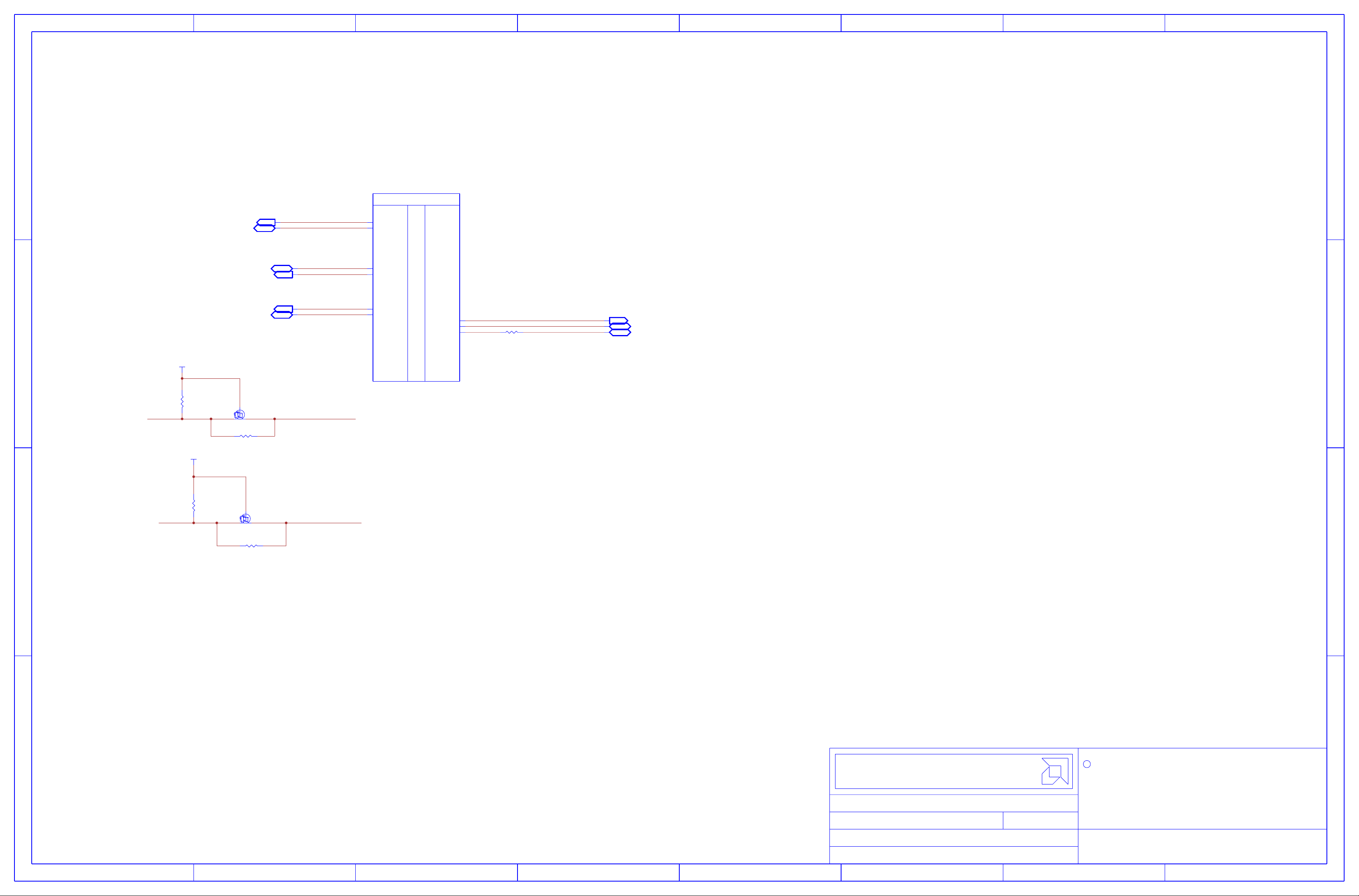
This AMD Board schematic and design is the exclusive property of AMD, and
DATE:
SHEET:
Advanced Micro Devices
2
3
345
6
6
7
7
8
8
C
5
CONFIDENTIAL AND PROPRIETARY TO ADVANCED MICRO DEVICES INC.
C
BB
A
1
DD
C
A
4
REV:
SHEET NUMBER:
DOCUMENT NUMBER:
OF
1
prohibited. Use of this schematic and design for any purpose other than
for evaluation purposes. Further distribution or disclosure is strictly
is provided only to entities under a non-disclosure agreement with AMD
2
schematic and design, including, not limited to, any implied warranty
AMD makes no representations or warranties of any kind regarding this
evaluation requires a Board Technology License Agreement with AMD.
of merchantability or fitness for a particular purpose, and disclaims
responsibility for any consequences resulting from use of the
information included herein.
TITLE:
BI
OUT
OUTBIBIBIOUT
OUT
BI
REV 0.90
PART 10 OF 18
SVI2&I2C
GPIO_SVD
GPIO_SVC
GPIO_SVT
SMBDAT
SMBCLK
DDCVGADATA
DDCVGACLK
SCL
SDA
8
7
6
345
2
1
(8) ELLESMERE DAC1 LOCK
(8) ELLESMERE DAC1 LOCK
24 1
24 1
OUT
1 24
1 24
BI
8
8
BI
8
8
OUT
G_SMBCLK
G_SMBCLK
G_SMBDAT
G_SMBDAT
SCL_S
SCL_S
SDA_S
SDA_S
AM34
AM34
AM33
AM33
AF34
AF34
AF33
AF33
SMBCLK
SMBDAT
SCL
SDA
U1
U1
PART 10 OF 18
SVI2&I2C
DD
DDCVGACLK
24
24
24
24
OUT
BI
DDCVGACLK
DDCVGADATA
DDCVGADATA
C
SCL_S
SCL_S
8
8
+1.8V
+1.8V
R1111
R1111
10K
10K
2 1
2 1
+1.8V
+1.8V
R1112
R1112
10K
10K
2 1
SDA_S
SDA_S
8
8
2 1
2
2
BSH111BK
BSH111BK
R1113
213
213
1
1
3
3
BSH111BK
BSH111BK
MQ1103
MQ1103
21R1113
21
MQ1105
MQ1105
SCL
SCL
0R
0R
SDA
SDA
AD34
AD34
AD33
AD33
22 24
22 24
DDCVGACLK
DDCVGADATA
REV 0.90
22 24
22 24
ellesmere_l4
ellesmere_l4
GPIO_SVC
GPIO_SVD
GPIO_SVT
AM23
AM23
AP23
AP23
AN23
AN23
PR9
PR9
VDDC_VDDCI_SVC
VDDC_VDDCI_SVC
VDDC_VDDCI_SVD
21
21
0R
0R
VDDC_VDDCI_SVD
VDDC_VDDCI_SVT
5%
5%
VDDC_VDDCI_SVT
OUT
BI
BI
22 14
22 14
22 14
22 14
14
14
C
A
R1114
21R1114
21
0R
0R
BB
AMD - PLATFORM HARDWARE ENG
AMD - PLATFORM HARDWARE ENG
#48, No.1387, ZHANGDONG ROAD
#48, No.1387, ZHANGDONG ROAD
SHANGHAI, CHINA 201203
SHANGHAI, CHINA 201203
SHEET:
DATE:
SHEET NUMBER:
DOCUMENT NUMBER:
ELLESMERE SVI2&I2C
ELLESMERE SVI2&I2C
Wed Apr 13 17:07:28 2016 1.0
Wed Apr 13 17:07:28 2016 1.0
8 26
8 26
OF
105_D009XX_00
105_D009XX_00
REV:
CONFIDENTIAL AND PROPRIETARY TO ADVANCED MICRO DEVICES INC.
2016
2016
C
This AMD Board schematic and design is the exclusive property of AMD, and
is provided only to entities under a non-disclosure agreement with AMD
for evaluation purposes. Further distribution or disclosure is strictly
prohibited. Use of this schematic and design for any purpose other than
evaluation requires a Board Technology License Agreement with AMD.
AMD makes no representations or warranties of any kind regarding this
schematic and design, including, not limited to, any implied warranty
of merchantability or fitness for a particular purpose, and disclaims
responsibility for any consequences resulting from use of the
information included herein.
TITLE:
Advanced Micro Devices
Ellesmere XT/PRO GD5 8L
Ellesmere XT/PRO GD5 8L
A
8
7
6
5
4
3
2
1
Page 9

This AMD Board schematic and design is the exclusive property of AMD, and
DATE:
SHEET:
Advanced Micro Devices
2
3
345
6
6
7
7
8
8
C
5
CONFIDENTIAL AND PROPRIETARY TO ADVANCED MICRO DEVICES INC.
C
BB
A
1
DD
C
A
4
REV:
SHEET NUMBER:
DOCUMENT NUMBER:
OF
1
prohibited. Use of this schematic and design for any purpose other than
for evaluation purposes. Further distribution or disclosure is strictly
is provided only to entities under a non-disclosure agreement with AMD
2
schematic and design, including, not limited to, any implied warranty
AMD makes no representations or warranties of any kind regarding this
evaluation requires a Board Technology License Agreement with AMD.
of merchantability or fitness for a particular purpose, and disclaims
responsibility for any consequences resulting from use of the
information included herein.
TITLE:
G4
G3
M3
M2
M1
G2
G1
TMDS_Clock-
TMDS_Clock+
TMDS_Clock_Shield
TMDS_Data5+
TMDS_Data5-
TMDS_Data0/5_Shield
TMDS_Data0+
TMDS_Data0-
Hot_Plug_Detect
GND_(for_+5V)
+5V_Power
TMDS_Data3+
TMDS_Data3-
TMDS_Data1/3_Shield
TMDS_Data1+
TMDS_Data1-
Analog_VSYNC
DDC_Data
DDC_Clock
TMDS_Data4+
TMDS_Data4-
TMDS_Data2/4_Shield
TMDS_Data2+
TMDS_Data2-
INBIOUT
OUT
REV 0.90
PART 11 OF 18
T
M
D
P
A
/
B
DP_ZVDD_08
DDCAUX4P
DDCAUX4N
DDCAUX6P
DDCAUX6N
TX1P_DPB1P
TX4P_DPA1P
TX1M_DPB1N
TX4M_DPA1N
TX0P_DPB2P
TX3P_DPA2P
TX2P_DPB0P
TX5P_DPA0P
TX0M_DPB2N
TX3M_DPA2N
TX2M_DPB0N
TX5M_DPA0N
AUX_ZVSSDP_ZVSS
TXCBP_DPB3P
TXCBM_DPB3N
TXCAP_DPA3P
TXCAM_DPA3N
8
7
6
345
2
1
(9) ELLESMERE TMDP A/B
(9) ELLESMERE TMDP A/B
C
+0.8V
+0.8V
R1718
R1700
21R1718
21
21R1700
200R
200R
21
200R
200R
1%
1%
DP_ZVDD_08
DP_ZVDD_08
1%
DP_ZVSS AUX_ZVSS
DP_ZVSS AUX_ZVSS
1%
AT36
AT36
AV36
AV36
DP_ZVDD_08
U1
U1
PART 11 OF 18
T
M
D
P
A
/
B
TX2P_DPB0P
TX2M_DPB0N
TX1P_DPB1P
TX1M_DPB1N
TX0P_DPB2P
TX0M_DPB2N
TXCBP_DPB3P
TXCBM_DPB3N
DDCAUX4P
DDCAUX4N
TX5P_DPA0P
TX5M_DPA0N
TX4P_DPA1P
TX4M_DPA1N
TX3P_DPA2P
TX3M_DPA2N
TXCAP_DPA3P
TXCAM_DPA3N
DDCAUX6P
DDCAUX6N
AUX_ZVSSDP_ZVSS
AY36
AY36
AY35
AY35
BC35
BC35
BB35
BB35
BB33
BB33
BC33
BC33
AY33
AY33
AY32
AY32
AU33
AU33
AT33
AT33
BB39
BB39
BC39
BC39
AY39
AY39
AY38
AY38
BC38
BC38
BB38
BB38
BB36
BB36
BC36
BC36
BC41
BC41
BB40
BB40
AY24
AY24
DDC4CLK_HDMI
DDC4CLK_HDMI
DDC4DAT_HDMI
DDC4DAT_HDMI
DPA_TX5P
DPA_TX5P
DPA_TX5N
DPA_TX5N
DPA_TX4P
DPA_TX4P
DPA_TX4N
DPA_TX4N
DPA_TX3P
DPA_TX3P
DPA_TX3N
DPA_TX3N
DDC6CLK_DVI
DDC6CLK_DVI
DDC6DATA_DVI
DDC6DATA_DVI
R1900
R1900
DPB_TX2P
DPB_TX2P
DPB_TX2N
DPB_TX2N
DPB_TX1P
DPB_TX1P
DPB_TX1N
DPB_TX1N
DPB_TX0P
DPB_TX0P
DPB_TX0N
DPB_TX0N
DPB_TXCAP
DPB_TXCAP
DPB_TXCAN
DPB_TXCAN
OUT
150R
150R
BI
6.3V
C1954
C1954
C1955
C1955
C1956
C1956
C1957
C1957
C1958
C1958
C1959
C1959
C1960
C1960
C1961
C1961
10
10
10
10
6.3V
C1920
C1920
C1921
C1921
C1922
C1922
C1923
C1923
C1924
C1924
C1925
C1925
+3.3V_BUS
+3.3V_BUS
R1940
R1940
10K
10K
5%
5%
+3.3V_BUS
+3.3V_BUS
R1941
R1941
10K
10K
5%
5%
4
4
1%
1%
0.1uF
0.1uF
0.1uF
0.1uF
0.1uF
0.1uF
0.1uF
0.1uF
0.1uF
0.1uF
0.1uF
0.1uF
1
1
5
5
6.3V
6.3V
6.3V
6.3V
6.3V
6.3V
6.3V
6.3V
6.3V
6.3V
6.3V
Q1980
Q1980
2
2
2N7002DW
2N7002DW
6
6
Q1980
Q1980
2N7002DW
2N7002DW
3
3
6.3V
0.1uF
0.1uF
6.3V
6.3V
0.1uF
0.1uF
6.3V
6.3V
0.1uF
0.1uF
6.3V
6.3V
0.1uF
0.1uF
6.3V
6.3V
0.1uF
0.1uF
6.3V
6.3V
0.1uF
0.1uF
6.3V
6.3V
0.1uF
0.1uF
6.3V
6.3V
0.1uF
0.1uF
+5V_VESA
+5V_VESA
DDC6CLK_DVI_L
DDC6CLK_DVI_L
DDC6DAT_DVI_L
DDC6DAT_DVI_L
2.2K
2.2K
5%
5%
R1986R1985
R1986R1985
2.2K
2.2K
5%
5%
R1990
R1990
R1991
R1991
5%33R
5%33R
33R 5%
33R 5%
10
IN
DVI_EN
DVI_EN
7
7
OUT
2
2
9
DDC6CLK_DVI_C
DDC6CLK_DVI_C
9
9
9
DDC6DATA_DVI_C
DDC6DATA_DVI_C
MMDT3904-7
MMDT3904-7
HPD3
HPD3
6
6
1
1
Q1951
Q1951
R1951
R1951
R1953
R1953
R1952
R1952
R1955
R1955
R1954
R1954
R1957
R1957
R1956
R1956
R1958
R1958
R1959
R1959
R1911
R1911
R1910
R1910
R1913
R1913
R1912
R1912
R1914
R1914
DPBA_GND
DPBA_GND
Q1820
Q1820
2N7002DW10
2N7002DW
+3.3V_BUS
+3.3V_BUS
4 3
4 3
5
5
499R 1%
499R 1%
499R 1%
499R 1%
499R 1%
499R 1%
499R 1%
499R 1%
499R 1%
499R 1%
499R 1%
499R 1%
499R 1%
499R 1%
499R
499R
499R
499R
499R
499R
499R
499R
R1915
R1915
R1916
R1916
1%499R
1%499R
1%499R
1%499R
1%499R
1%499R
1%
1%
1%
1%
1%
1%
1%
1%
+5V_VESA
+5V_VESA
5%10K
5%10K
5%10K
5%10K
C1926
C1926
1uF
1uF
16V
16V
EFTX2M
EFTX2M
9
9
EFTX2P
EFTX2P
9
9
EFTX4M
EFTX4M
9
9
EFTX4P
EFTX4P
9
9
EFTX1M
EFTX1M
9
9
EFTX1P
EFTX1P
9
9
EFTX3M
EFTX3M
9
9
EFTX3P
EFTX3P
9
9
+5V_VESA
+5V_VESA
HPD_EF_DVI
HPD_EF_DVI
EFTX0M
EFTX0M
9
9
EFTX0P
EFTX0P
9
9
EFTX5M
EFTX5M
9
9
EFTX5P
EFTX5P
9
9
EFTXCP
EFTXCP
9
9
EFTXCM
EFTXCM
9
9
EFTX2P
EFTX2P
EFTX2M
EFTX2M
EFTX1P
EFTX1P
EFTX1M
EFTX1M
EFTX0P
EFTX0P
EFTX0M
EFTX0M
EFTXCP
EFTXCP
EFTXCM
EFTXCM
EFTX5P
EFTX5P
EFTX5M
EFTX5M
EFTX4P
EFTX4P
EFTX4M
EFTX4M
EFTX3P
EFTX3P
EFTX3M
EFTX3M
1
1
TMDS_Data2-
2
2
TMDS_Data2+
3
3
TMDS_Data2/4_Shield
4
4
TMDS_Data4-
5
5
TMDS_Data4+
6
6
DDC_Clock
7
7
DDC_Data
8
8
Analog_VSYNC
9
9
TMDS_Data1-
10
10
TMDS_Data1+
11
11
TMDS_Data1/3_Shield
12
12
TMDS_Data3-
13
13
TMDS_Data3+
14
14
+5V_Power
15
15
GND_(for_+5V)
16
16
Hot_Plug_Detect
17
17
TMDS_Data0-
18
18
TMDS_Data0+
19
19
TMDS_Data0/5_Shield
20
20
TMDS_Data5-
21
21
TMDS_Data5+
22
22
TMDS_Clock_Shield
23
23
TMDS_Clock+
24
24
TMDS_Clock-
9
9
9
9
9
9
9
9
9
9
9
9
9
9
9
9
9
9
9
9
9
9
9
9
9
9
9
9
J1950
J1950
G1
G1
G1
G2
G2
G2
G3
G3
G3
G4
G4
G4
M1
M1
M1
M2
M2
M2
M3
M3
M3
DD
C
SCREW1950
SCREW1950
SCREW1951
SCREW1951
A
DVI-D
DVI-D
OPTIONAL ESD PROTECTION DIODES
OPTIONAL ESD PROTECTION DIODES
D1950
8
D1950
D1901
D1901
D1952
D1952
D1903
D1903
D1904
D1904
D1905
D1905
D1906
D1906
D1967
D1967
D1968
D1968
D1969
D1969
D1910
D1910
D1911
D1911
D1912
D1912
D1913
D1913
D1503
D1503
D1504
D1504
12
12
ESD5V3U1U-02LRH
ESD5V3U1U-02LRH
12
12
ESD5V3U1U-02LRH
ESD5V3U1U-02LRH
12
12
ESD5V3U1U-02LRH
ESD5V3U1U-02LRH
12
12
ESD5V3U1U-02LRH
ESD5V3U1U-02LRH
ESD5V3U1U-02LRH
ESD5V3U1U-02LRH
12
12
ESD5V3U1U-02LRH
ESD5V3U1U-02LRH
12
12
ESD5V3U1U-02LRH
ESD5V3U1U-02LRH
12
12
ESD5V3U1U-02LRH
ESD5V3U1U-02LRH
12
12
ESD5V3U1U-02LRH
ESD5V3U1U-02LRH
12
12
ESD5V3U1U-02LRH
ESD5V3U1U-02LRH
12
12
ESD5V3U1U-02LRH
ESD5V3U1U-02LRH
12
12
ESD5V3U1U-02LRH
ESD5V3U1U-02LRH
12
12
ESD5V3U1U-02LRH
12
ESD5V3U1U-02LRH
12
12
ESD5V3U1U-02LRH
ESD5V3U1U-02LRH
12
12
ESD8V0R1B-02LRH
ESD8V0R1B-02LRH
12
ESD8V0R1B-02LRH
ESD8V0R1B-02LRH
12
12
DDC6DATA_DVI_C
DDC6DATA_DVI_C
DDC6CLK_DVI_C
DDC6CLK_DVI_C
EFTX2P
EFTX2P
EFTX2M
EFTX2M
EFTX1P
EFTX1P
EFTX1M
EFTX1M
EFTX0P
EFTX0P
EFTX0M
EFTX0M
EFTXCP
EFTXCP
EFTXCM
EFTXCM
EFTX5P
EFTX5P
EFTX5M
EFTX5M
EFTX4P
EFTX4P
EFTX4M
EFTX4M
EFTX3P
EFTX3P
EFTX3M
EFTX3M
7
ellesmere_l4
ellesmere_l4
9
9
9
9
9
9
9
9
9
9
9
9
9
9
9
9
9
9
9
9
9
9
9
9
9
9
9
9
9
9
9
9
REV 0.90
6140168000G
6140168000G
CONFIDENTIAL AND PROPRIETARY TO ADVANCED MICRO DEVICES INC.
2016
2016
AMD - PLATFORM HARDWARE ENG
AMD - PLATFORM HARDWARE ENG
#48, No.1387, ZHANGDONG ROAD
#48, No.1387, ZHANGDONG ROAD
SHANGHAI, CHINA 201203
SHANGHAI, CHINA 201203
SHEET:
DATE:
SHEET NUMBER:
DOCUMENT NUMBER:
6
5
4
ELLESMERE TMDPAB dDVI
ELLESMERE TMDPAB dDVI
Wed Apr 13 17:02:08 2016 1.0
Wed Apr 13 17:02:08 2016 1.0
9 26
9 26
OF
105_D009XX_00
105_D009XX_00
REV:
3
C
This AMD Board schematic and design is the exclusive property of AMD, and
is provided only to entities under a non-disclosure agreement with AMD
for evaluation purposes. Further distribution or disclosure is strictly
prohibited. Use of this schematic and design for any purpose other than
evaluation requires a Board Technology License Agreement with AMD.
AMD makes no representations or warranties of any kind regarding this
schematic and design, including, not limited to, any implied warranty
of merchantability or fitness for a particular purpose, and disclaims
responsibility for any consequences resulting from use of the
information included herein.
TITLE:
2
Advanced Micro Devices
Ellesmere XT/PRO GD5 8L
Ellesmere XT/PRO GD5 8L
1
BB
A
Page 10

This AMD Board schematic and design is the exclusive property of AMD, and
DATE:
SHEET:
Advanced Micro Devices
2
3
345
6
6
7
7
8
8
C
5
CONFIDENTIAL AND PROPRIETARY TO ADVANCED MICRO DEVICES INC.
C
BB
A
1
DD
C
A
4
REV:
SHEET NUMBER:
DOCUMENT NUMBER:
OF
1
prohibited. Use of this schematic and design for any purpose other than
for evaluation purposes. Further distribution or disclosure is strictly
is provided only to entities under a non-disclosure agreement with AMD
2
schematic and design, including, not limited to, any implied warranty
AMD makes no representations or warranties of any kind regarding this
evaluation requires a Board Technology License Agreement with AMD.
of merchantability or fitness for a particular purpose, and disclaims
responsibility for any consequences resulting from use of the
information included herein.
TITLE:
Y4
Y3
GND1
Y2
Y1
D
C
A
GND
B
Y4
Y3
GND1
Y2
Y1
D
C
A
GND
B
CASE
CASE
CASE
CASE
Hot Plog Detect
+5V Pwr
GND (+5V)
DDC Data
DDC Clock
NC
CEC
TMDS Clock-
Clk Shld
TMDS Clock+
TMDS Data 0-
D0 Shld
TMDS Data 0+
TMDS Data 1-
D1 Shld
TMDS Data 1+
TMDS Data 2-
D2 Shld
TMDS Data 2+
OUT
OUTINBI
DP_PWR
GND_6
GND_2
GND_3
GND_0
GND_1
G4
G3
G2
G1
PWR_RTN
ML_Lane_0p
ML_Lane_0n
ML_Lane_3n
ML_Lane_2n
ML_Lane_1n
ML_Lane_3p
ML_Lane_2p
ML_Lane_1p
AUX_CHp
AUX_CHn
Hot_Det
CONFIG 1
CONFIG 2
SCREW
OUT
Y4
Y3
GND1
Y2
Y1
D
C
A
GND
B
Y4
Y3
GND1
Y2
Y1
D
C
A
GND
B
REV 0.90
PART 12 OF 18
T
M
D
P
C
/
D
DDC2DATA
DDC2CLK
AUX2N
AUX2P
DDCAUX5P
DDCAUX5N
TX1M_DPD1N
TX4M_DPC1N
TX0P_DPD2P
TX3P_DPC2P
TX2P_DPD0P
TX5P_DPC0P
TX0M_DPD2N
TX3M_DPC2N
TX2M_DPD0N
TX5M_DPC0N
TX1P_DPD1P
TX4P_DPC1P
TXCDP_DPD3P
TXCDM_DPD3N
TXCCP_DPC3P
TXCCM_DPC3N
8
7
6
345
2
1
+3.3V_DPDC
+3.3V_DPDC
SCREW1700
SCREW1700
C1737
C1737
1uF
1uF
6.3V
6.3V
DD
SCREW
C
BB
R1706
R1706
10
10
10
10
10
10
10
10
10
10
10
10
10
10
10
10
5.1M
5.1M
DTX2P
DTX2P
DTX2N
DTX2N
DTX1P
DTX1P
DTX1N
DTX1N
DTX0P
DTX0P
DTX0N
DTX0N
DTXCAP
DTXCAP
DTXCAN
DTXCAN
J1700
J1700
1
1
ML_Lane_0p
3
3
ML_Lane_0n
4
4
ML_Lane_1p
6
6
ML_Lane_1n
7
7
ML_Lane_2p
9
9
ML_Lane_2n
10
10
ML_Lane_3p
12
12
ML_Lane_3n
15
15
AUX_CHp
17
17
AUX_CHn
18
18
Hot_Det
13
13
CONFIG 1
5%
5%
14
14
CONFIG 2
DP_W/GASKET
DP_W/GASKET
1
1
3
3
4
4
6
6
7
7
9
9
10
10
12
12
15
15
16
16
19
19
14
14
13
13
DP_PWR
PWR_RTN
GND_0
GND_1
GND_2
GND_3
GND_6
6140073700G
6140073700G
J2501
J2501
TMDS Data 2+
TMDS Data 2TMDS Data 1+
TMDS Data 1TMDS Data 0+
TMDS Data 0TMDS Clock+
TMDS Clock-
DDC Clock
DDC Data
Hot Plog Detect
NC
CEC
GND (+5V)
HDMI_W/TAB
HDMI_W/TAB
G1
G2
G3
G4
+5V Pwr
D0 Shld
D1 Shld
D2 Shld
Clk Shld
CASE
CASE
CASE
CASE
20
20
19
19
G1
G1
G2
G2
G3
G3
G4
G4
2
2
5
5
8
8
11
11
16
16
C1828
C1828
22uF
22uF
6.3V
6.3V
+5V_VESA
+5V_VESA
18
18
8
8
5
5
2
2
11
11
17
17
20
20
21
21
22
22
23
23
MMDT3904-7
MMDT3904-7
21
21
100nH
100nH
21
21
100nH
100nH
21
21
100nH
100nH
21
21
100nH
100nH
21
21
100nH
100nH
21
21
100nH
100nH
21
21
100nH
100nH
21
21
100nH
100nH
DPE_GND
DPE_GND
Q1820
Q1820
2N7002DW
2N7002DW
10
10
10
10
+3.3V_BUS
+3.3V_BUS
Q1700
Q1700
1 6
1 6
R1825
R1825
R1824
R1824
R1823
R1823
R1822
R1822
R1821
R1821
R1820
R1820
R1819
R1819
R1818
R1818
DDC4CLK_HDMI_C
DDC4CLK_HDMI_C
DDC4DAT_HDMI_C
DDC4DAT_HDMI_C
+3.3V_BUS
+3.3V_BUS
Q1823
Q1823
MMBT3904
MMBT3904
HPD5
HPD5
10
DPD_0P
10
DPD_0P
10
10
DPD_0N
DPD_0N
DPD_1P
10
DPD_1P
10
10
DPD_1N
10
DPD_1N
10
10
DPD_2P
DPD_2P
10
10
DPD_2N
DPD_2N
10
10
DPD_3P
DPD_3P
10
10
DPD_3N
DPD_3N
10
10
AUX2P_DPA
5%
10K
10K
10K 5%
10K 5%
1%
1%
100K
100K
100K
100K
1M
1M
5%
5%
5%
5%
R1880
R1881
R1882
R1883
R1884
R1885
R1886
R1887
10K
10K
5%
5%
5%
R1702
R1702
R1703
R1703
2
2
R1707
R1707
R1708
R1708
R1701
R1701
499R 1%
499R 1%
499R 1%
499R 1%
499R 1%
499R 1%
499R 1%
499R 1%
499R 1%
499R 1%
499R 1%
499R 1%
499R 1%
499R 1%
499R
499R
1
1
R1829
R1829
2 3
2 3
R1828
R1828
AUX2P_DPA
10
10
AUX2N_DPA
AUX2N_DPA
+3.3V_DPDC
+3.3V_DPDC
HPD_DPA
HPD_DPA
10
10
DPA_DONGLE_DET
DPA_DONGLE_DET
21R1880
21
21R1881
21
21R1882
21
21R1883
21
21R1884
21
21R1885
21
21R1886
21
3.3R
3.3R
21R1887
21
3.3R 1%
3.3R 1%
5%
5%
5%10K
5%10K
1%3.3R
1%3.3R
1%3.3R
1%3.3R
1%3.3R
1%3.3R
1%3.3R
1%3.3R
1%3.3R
1%3.3R
1%3.3R
1%3.3R
1%
1%
HPD_HDMI
HPD_HDMI
(10) ELLESMERE TMDP C/D
(10) ELLESMERE TMDP C/D
C
U1
U1
PART 12 OF 18
BB27
AUX2P
AUX2N
BB27
BC27
BC27
AY27
AY27
AY26
AY26
BC26
BC26
BB26
BB26
BB25
BB25
BC25
BC25
AV25
AV25
AW25
AW25
AU26
AU26
AV26
AV26
BC32
BC32
BB32
BB32
BB30
BB30
BC30
BC30
AY30
AY30
AY29
AY29
BC29
BC29
BB29
BB29
AU35
AU35
AV35
AV35
T
M
D
P
C
/
D
ellesmere_l4
ellesmere_l4
TX2P_DPD0P
TX2M_DPD0N
TX1P_DPD1P
TX1M_DPD1N
TX0P_DPD2P
TX0M_DPD2N
TXCDP_DPD3P
TXCDM_DPD3N
DDC2CLK
DDC2DATA
TX5P_DPC0P
TX5M_DPC0N
TX4P_DPC1P
TX4M_DPC1N
TX3P_DPC2P
TX3M_DPC2N
TXCCP_DPC3P
TXCCM_DPC3N
DDCAUX5P
DDCAUX5N
REV 0.90
DPD_C0P
DPD_C0P
DPD_C0N
DPD_C0N
DPD_C1P
DPD_C1P
DPD_C1N
DPD_C1N
DPD_C2P
DPD_C2P
DPD_C2N
DPD_C2N
DPD_C3P
DPD_C3P
DPD_C3N
DPD_C3N
AUX2P
AUX2P
AUX2N
AUX2N
DDC2CLK
DDC2CLK
DDC2DATA
DDC2DATA
DPC_TX2P
DPC_TX2P
DPC_TX2N
DPC_TX2N
DPC_TX1P
DPC_TX1P
DPC_TX1N
DPC_TX1N
DPC_TX0P
DPC_TX0P
DPC_TX0N
DPC_TX0N
DPC_TXCP
DPC_TXCP
DPC_TXCN
DPC_TXCN
Q1701
Q1701
2N7002DW
2N7002DW
1
1
2
2
C1731
C1731
C1732
C1732
6
6
4
3
3
4
Q1701
Q1701
2N7002DW
2N7002DW
5
5
9
9
IN
9
9
BI
C1720
C1720
C1721
C1721
C1722
C1722
C1723
C1723
C1724
C1724
C1725
C1725
C1726
C1726
C1727
C1727
0.1uF
0.1uF
0.1uF
0.1uF
C1829
C1829
C1830
C1830
C1831
C1831
C1832
C1832
C1833
C1833
C1834
C1834
C1835
C1835
C1836
C1836
DDC4CLK_HDMI
DDC4CLK_HDMI
DDC4DAT_HDMI
DDC4DAT_HDMI
0.1uF
0.1uF
0.1uF
0.1uF
0.1uF
0.1uF
0.1uF
0.1uF
0.1uF
0.1uF
0.1uF
0.1uF
0.1uF
0.1uF
0.1uF
0.1uF
6.3V
6.3V
6.3V
6.3V
0.1uF
0.1uF
0.1uF
0.1uF
0.1uF
0.1uF
0.1uF
0.1uF
0.1uF
0.1uF
0.1uF
0.1uF
0.1uF
0.1uF
0.1uF
0.1uF
6.3V
6.3V
6.3V
6.3V
6.3V
6.3V
6.3V
6.3V
6.3V
6.3V
6.3V
6.3V
6.3V
6.3V
6.3V
6.3V
AUX2_BYPSS_EN
AUX2_BYPSS_EN
6.3V
6.3V
6.3V
6.3V
6.3V
6.3V
6.3V
6.3V
6.3V
6.3V
6.3V
6.3V
6.3V
6.3V
6.3V
6.3V
+3.3V_BUS
+3.3V_BUS
R1840
R1840
10K
10K
5%
5%
+3.3V_BUS
+3.3V_BUS
R1841
R1841
10K
10K
5%
5%
1
Q1810
Q1810
5
5
2N7002DW
2N7002DW
3
3
Q1810
Q1810
2
2
2N7002DW
2N7002DW
6
6
MMDT3904-7
MMDT3904-7
+5V_VESA
+5V_VESA
2.2K
2.2K
DDC4CLK_HDMI_L
DDC4CLK_HDMI_L
DDC4DAT_HDMI_L
DDC4DAT_HDMI_L
+12V_BUS
+12V_BUS
Q1700
Q1700
+12V_BUS
+12V_BUS
R1831R1830
R1831R1830
2.2K
2.2K
5%5%
5%5%
+12V_BUS
+12V_BUS
R1705R1704
R1705R1704
10K
9
9
R1817
R1817
R1810
R1811
10K
5%
5%
3
3
2
2
OUT
100K
100K
1
1
Q1704
Q1704
2N7002E
2N7002E
5%
5%
33R
33R
21R1810
211
7
7
DVI_EN
DVI_EN
C1827
C1827
0.1uF
0.1uF
16V
16V
5%
5%
214
21R18114
OUT
5%33R
5%33R
5
5
HPD1
HPD1
L1880
L1880
L1881
L1881
L1882
L1882
L1883
L1883
L1884
L1884
L1885
L1885
L1886
L1886
L1887
L1887
7
7
OUT
3
3
4
4
10K
10K
5%
5%
5
5
4 3
4 3
A
8
OPTIONAL ESD PROTECTION DIODES
OPTIONAL ESD PROTECTION DIODES
D1700
D1700
DPD_0P
DPD_0P
10
10
DPD_0N
DPD_0N
10
10
DPD_1P
DPD_1P
10
10
DPD_1N
DPD_1N
10
10
DPD_3N
DPD_3N
10
10
DPD_3P
DPD_3P
10
10
DPD_2N DPD_2N
DPD_2N DPD_2N
10 10
10 10
D1709
D1709
D1708
D1708
D1707
D1707
5
5
D
4
4
C
GND
2
2
B
1
1
A
RCLAMP0524P
RCLAMP0524P
D1702
D1702
5
5
D
4
4
C
GND
2
2
B
1
1
A
RCLAMP0524P
RCLAMP0524P
12
ESD5V3U1U-02LRH
ESD5V3U1U-02LRH
12
12
ESD5V3U1U-02LRH
ESD5V3U1U-02LRH
12
12
ESD5V3U1U-02LRH
ESD5V3U1U-02LRH
12
GND1
GND1
6
6
Y4
7
7
Y3
83
83
9
9
Y2
10
10
Y1
6
6
Y4
7
7
Y3
83
83
9
9
Y2
10
10
Y1
DPD_0P
DPD_0P
10
10
DPD_0N
DPD_0N
10
10
DPD_1P
DPD_1P
10
10
DPD_1N
DPD_1N
10
10
DPD_3N
DPD_3N
10
10
DPD_3P
DPD_3P
10
10
DPD_2PDPD_2P
DPD_2PDPD_2P
10 10
10 10
AUX2P_DPA
AUX2P_DPA
AUX2N_DPA
AUX2N_DPA
DPA_DONGLE_DET
DPA_DONGLE_DET
7
10
10
10
10
10
10
10
10
10
10
10
10
10
10
10
10
10
10
10
10
10
10
DTX2P
DTX2P
DTX2N
DTX2N
DTX1P
DTX1P
DTX1N
DTX1N
DTXCAN
DTXCAN
DTXCAP
DTXCAP
DTX0N
DTX0N
DTX0P
DTX0P
D1862
D1862
D1863
D1863
5
5
D
4
4
C
GND
2
2
B
1
1
A
5
5
D
4
4
C
GND
2
2
B
1
1
A
12
12
ESD5V3U1U-02LRH
ESD5V3U1U-02LRH
12
12
ESD5V3U1U-02LRH
ESD5V3U1U-02LRH
D1850
D1850
D1851
D1851
GND1
GND1
6
6
6
Y4
7
7
Y3
83
83
9
9
Y2
10
10
Y1
DNIRCLAMP0524P
DNIRCLAMP0524P
6
6
Y4
7
7
Y3
83
83
9
9
Y2
10
10
Y1
DNIRCLAMP0524P
DNIRCLAMP0524P
DNI
DNI
DNI
DNI
DTX2P
DTX2P
DTX2N
DTX2N
DTX1P
DTX1P
DTX1N
DTX1N
DTXCAN
DTXCAN
DTXCAP
DTXCAP
DTX0N
DTX0N
DTX0P
DTX0P
DDC4CLK_HDMI_C
DDC4CLK_HDMI_C
DDC4DAT_HDMI_C
DDC4DAT_HDMI_C
10
10
10
10
10
10
10
10
10
10
10
10
10
10
10
10
10
10
10
10
CONFIDENTIAL AND PROPRIETARY TO ADVANCED MICRO DEVICES INC.
2016
2016
AMD - PLATFORM HARDWARE ENG
AMD - PLATFORM HARDWARE ENG
#48, No.1387, ZHANGDONG ROAD
#48, No.1387, ZHANGDONG ROAD
SHANGHAI, CHINA 201203
SHANGHAI, CHINA 201203
SHEET:
DATE:
SHEET NUMBER:
DOCUMENT NUMBER:
5
4
ELLESMERE TMDPCD DP HDMI
ELLESMERE TMDPCD DP HDMI
Wed Apr 13 17:02:09 2016
Wed Apr 13 17:02:09 2016 1.0
10 26
10 26
OF
105_D009XX_00
105_D009XX_00
REV:
3
1.0
C
This AMD Board schematic and design is the exclusive property of AMD, and
is provided only to entities under a non-disclosure agreement with AMD
for evaluation purposes. Further distribution or disclosure is strictly
prohibited. Use of this schematic and design for any purpose other than
evaluation requires a Board Technology License Agreement with AMD.
AMD makes no representations or warranties of any kind regarding this
schematic and design, including, not limited to, any implied warranty
of merchantability or fitness for a particular purpose, and disclaims
responsibility for any consequences resulting from use of the
information included herein.
TITLE:
2
Advanced Micro Devices
Ellesmere XT/PRO GD5 8L
Ellesmere XT/PRO GD5 8L
1
A
Page 11

This AMD Board schematic and design is the exclusive property of AMD, and
DATE:
SHEET:
Advanced Micro Devices
2
3
345
6
6
7
7
8
8
C
5
CONFIDENTIAL AND PROPRIETARY TO ADVANCED MICRO DEVICES INC.
C
BB
A
1
DD
C
A
4
REV:
SHEET NUMBER:
DOCUMENT NUMBER:
OF
1
prohibited. Use of this schematic and design for any purpose other than
for evaluation purposes. Further distribution or disclosure is strictly
is provided only to entities under a non-disclosure agreement with AMD
2
schematic and design, including, not limited to, any implied warranty
AMD makes no representations or warranties of any kind regarding this
evaluation requires a Board Technology License Agreement with AMD.
of merchantability or fitness for a particular purpose, and disclaims
responsibility for any consequences resulting from use of the
information included herein.
TITLE:
REV 0.90
PART 13 OF 18
F
/
E
TMDP
DDCAUX3P
DDCAUX3N
DDC1DATA
DDC1CLK
AUX1N
AUX1P
TX1M_DPF1N
TX4M_DPE1N
TX0P_DPF2P
TX3P_DPE2P
TX2P_DPF0P
TX5P_DPE0P
TX0M_DPF2N
TX3M_DPE2N
TX2M_DPF0N
TX5M_DPE0N
TX1P_DPF1P
TX4P_DPE1P
TXCFP_DPF3P
TXCFM_DPF3N
TXCEP_DPE3P
TXCEM_DPE3N
DP_PWR
GND_6
GND_2
GND_3
GND_0
GND_1
G4
G3
G2
G1
PWR_RTN
ML_Lane_0p
ML_Lane_0n
ML_Lane_3n
ML_Lane_2n
ML_Lane_1n
ML_Lane_3p
ML_Lane_2p
ML_Lane_1p
AUX_CHp
AUX_CHn
Hot_Det
CONFIG 1
CONFIG 2
SCREW
OUT
Y4
Y3
GND1
Y2
Y1
D
C
A
GND
B
Y4
Y3
GND1
Y2
Y1
D
C
A
GND
B
SCREW
DP_PWR
GND_6
GND_2
GND_3
GND_0
GND_1
G4
G3
G2
G1
PWR_RTN
ML_Lane_0p
ML_Lane_0n
ML_Lane_3n
ML_Lane_2n
ML_Lane_1n
ML_Lane_3p
ML_Lane_2p
ML_Lane_1p
AUX_CHp
AUX_CHn
Hot_Det
CONFIG 1
CONFIG 2
OUT
Y4
Y3
GND1
Y2
Y1
D
C
A
GND
B
Y4
Y3
GND1
Y2
Y1
D
C
A
GND
B
8
7
6
345
2
1
(11) ELLESMERE LVTMDP E/F
(11) ELLESMERE LVTMDP E/F
PART 13 OF 18
E
/
F
U1
U1
TMDP
TX2P_DPF0P
TX2M_DPF0N
TX1P_DPF1P
TX1M_DPF1N
TX0P_DPF2P
TX0M_DPF2N
TXCFP_DPF3P
TXCFM_DPF3N
AUX1P
AUX1N
DDC1CLK
DDC1DATA
BC21
BC21
BB21
BB21
BB20
BB20
BC20
BC20
BA20
BA20
BA19
BA19
BC19
BC19
BB19
BB19
AV23
AV23
AW23
AW23
AT23
AT23
AR23
AR23
DPF_C0P
DPF_C0P
DPF_C0N
DPF_C0N
DPF_C1P
DPF_C1P
DPF_C1N
DPF_C1N
DPF_C2P
DPF_C2P
DPF_C2N
DPF_C2N
DPF_C3P
DPF_C3P
DPF_C3N
DPF_C3N
DDCCLK_AUX1P
DDCCLK_AUX1P
DDCDATA_AUX1N
DDCDATA_AUX1N
Q1801
Q1801
2N7002DW
2N7002DW
1
1
6
6
2
2
453
4
5
C1801
C1801
C1802
C1802
C1805
C1805
C1806
C1806
C1807
C1807
C1808
C1808
C1809
C1809
C1810
C1810
C1811
C1811
C1812
C1812
3
Q1801
Q1801
2N7002DW
2N7002DW
0.1uF
0.1uF
0.1uF
0.1uF
0.1uF
0.1uF
0.1uF
0.1uF
0.1uF
0.1uF
0.1uF
0.1uF
0.1uF
0.1uF
0.1uF
0.1uF
0.1uF
0.1uF
0.1uF
0.1uF
6.3V
6.3V
6.3V
6.3V
6.3V
6.3V
6.3V
6.3V
6.3V
6.3V
6.3V
6.3V
6.3V
6.3V
6.3V
6.3V
6.3V
6.3V
6.3V
6.3V
+12V_BUS +12V_BUS
+12V_BUS +12V_BUS
Q1800
Q1800
MMDT3904-7
MMDT3904-7
R1804
R1804
10K
10K
5%
5%
4 3
4 3
J1800
J1800
11
11
DPF_0P
DPF_0P
11
11
DPF_0N
DPF_0N
11
11
DPF_1P
DPF_1P
11
11
DPF_1N
DPF_1N
11
11
DPF_2P
DPF_2P
11
11
DPF_2N
DPF_2N
11
11
DPF_3P
DPF_3P
11
11
DPF_3N
DPF_3N
11
11
AUX1P_DPC
100K 5%
R1802
R1802
R1803
+3.3V_BUS
+3.3V_BUS
Q1800
R1805
R1805
10K
10K
5%
5%
3
3
2
2
5
5
1
1
Q1804
Q1804
2N7002E
2N7002E
7
7
OUT
HPD6
HPD6
Q1800
MMDT3904-7
MMDT3904-7
R1803
2
2
R1807
R1807
1 6
1 6
R1808
R1808
R1801
R1801
100K 5%
100K 5%
100K 5%
10K 5%
10K 5%
5%10K
5%10K
1M 5%
1M 5%
AUX1P_DPC
11
11
AUX1N_DPC
AUX1N_DPC
+3.3V_DPF
+3.3V_DPF
HPD_DPF
HPD_DPF
DPF_DONGLE_DETAUX1_BYPSS_EN
DPF_DONGLE_DETAUX1_BYPSS_EN
R1806
R1806
1
1
ML_Lane_0p
3
3
ML_Lane_0n
4
4
ML_Lane_1p
6
6
ML_Lane_1n
7
7
ML_Lane_2p
9
9
ML_Lane_2n
10
10
ML_Lane_3p
12
12
ML_Lane_3n
15
15
AUX_CHp
17
17
AUX_CHn
18
18
Hot_Det
13
13
CONFIG 1
5%5.1M
5%5.1M
14
14
CONFIG 2
DP_W/GASKET
DP_W/GASKET
DP_PWR
PWR_RTN
GND_0
GND_1
GND_2
GND_3
GND_6
+3.3V_DPF
+3.3V_DPF
+3.3V_BUS
+3.3V_BUS
F1800
C1840
C1840
100uF
100uF
6.3V
6.3V
F1800
2 1
2 1
1.5A
1.5A
20
20
C1817
C1817
22uF
22uF
6.3V
6.3V
SCREW1800
SCREW1800
SCREW
19
19
G1
G1
G1
G2
G2
G2
G3
G3
G3
G4
G4
G4
2
2
5
5
8
8
11
11
16
16
DD
+3.3V_DPDC
C
BA25
REV 0.90
ellesmere_l4
ellesmere_l4
TX5P_DPE0P
TX5M_DPE0N
TX4P_DPE1P
TX4M_DPE1N
TX3P_DPE2P
TX3M_DPE2N
TXCEP_DPE3P
TXCEM_DPE3N
DDCAUX3P
DDCAUX3N
BA25
BA24
BA24
BC24
BC24
BB24
BB24
BB23
BB23
BC23
BC23
AY23
AY23
AY21
AY21
AU27
AU27
AV27
AV27
DPE_C0P
DPE_C0P
DPE_C0N
DPE_C0N
DPE_C1P
DPE_C1P
DPE_C1N
DPE_C1N
DPE_C2P
DPE_C2P
DPE_C2N
DPE_C2N
DPE_C3P
DPE_C3P
DPE_C3N
DPE_C3N
DDCCLK_AUX3P
DDCCLK_AUX3P
DDCDATA_AUX3N
DDCDATA_AUX3N
Q1901
2N7002DW 2N7002DW
2N7002DW 2N7002DW
126
Q1902
Q1902Q1901
6
6126
1
1
2
2
4
C1901
C1901
C1902
C1902
C1905
C1905
C1906
C1906
C1907
C1907
C1908
C1908
C1909
C1909
C1910
C1910
C1911
C1911
C1912
C1912
3
2N7002DW
2N7002DW
5
Q1901
Q1901
0.1uF
0.1uF
0.1uF
0.1uF
0.1uF
0.1uF
0.1uF
0.1uF
0.1uF
0.1uF
0.1uF
0.1uF
0.1uF
0.1uF
0.1uF
0.1uF
0.1uF
0.1uF
0.1uF
0.1uF
6.3V
6.3V
6.3V
6.3V
6.3V
6.3V
6.3V
6.3V
6.3V
6.3V
6.3V
6.3V
6.3V
6.3V
6.3V
6.3V
6.3V
6.3V
6.3V
6.3V
Q1902
Q1902
2N7002DW
2N7002DW
4
4
3
3453
5
5
AUX3_BYPSS_EN
AUX3_BYPSS_EN
+12V_BUS
+12V_BUS
Q1900
Q1900
MMDT3904-7
MMDT3904-7
R1904
R1904
10K
10K
5%
5%
4 3
4 3
5
5
+12V_BUS
+12V_BUS
R1905
R1905
10K
10K
5%
5%
3
3
2
2
1
1
Q1904
Q1904
2N7002E
2N7002E
J1900
J1900
11
11
DPE_0P
DPE_0P
11
11
DPE_0N
DPE_0N
11
11
DPE_1P
DPE_1P
11
11
DPE_1N
DPE_1N
11
11
DPE_2P
DPE_2P
11
11
DPE_2N
DPE_2N
11
11
DPE_3P
DPE_3P
11
11
DPE_3N
DPE_3N
11
11
AUX3P_DPC
5%100K
100K
100K
5%100K
5%
5%
5%10K
5%10K
5%10K
5%10K
5%1M
5%1M
R1902
R1902
R1903
+3.3V_BUS
+3.3V_BUS
Q1900
Q1900
MMDT3904-7
MMDT3904-7
HPD4
7
7
OUT
HPD4
R1903
2
2
R1907
R1907
1 6
1 6
R1908
R1908
R1901
R1901
AUX3P_DPC
11
11
AUX3N_DPC
AUX3N_DPC
+3.3V_DPDC
+3.3V_DPDC
HPD_DPE
HPD_DPE
11
11
DPE_DONGLE_DET
DPE_DONGLE_DET
R1906
R1906
1
1
ML_Lane_0p
3
3
ML_Lane_0n
4
4
ML_Lane_1p
6
6
ML_Lane_1n
7
7
ML_Lane_2p
9
9
ML_Lane_2n
10
10
ML_Lane_3p
12
12
ML_Lane_3n
15
15
AUX_CHp
17
17
AUX_CHn
18
18
Hot_Det
13
13
CONFIG 1
5%5.1M
5%5.1M
14
14
CONFIG 2
DP_W/GASKET
DP_W/GASKET
PWR_RTN
6140073700G
6140073700G
DP_PWR
G1
G2
G3
G4
GND_0
GND_1
GND_2
GND_3
GND_6
20
20
C1917
C1917
22uF
22uF
6.3V
6.3V
19
19
G1
G1
G2
G2
G3
G3
G4
G4
2
2
5
5
8
8
11
11
16
16
+3.3V_DPDC
SCREW1900
SCREW1900
SCREW
F1900
F1900
2 1
2 1
1.5A
1.5A
+3.3V_BUS
+3.3V_BUS
C
BB
A
OPTIONAL ESD PROTECTION DIODES
OPTIONAL ESD PROTECTION DIODES
DPF_0P
DPF_0P DPF_0P
11 11
11 11
DPF_0N
DPF_0N
11
11
DPF_1P
DPF_1P
11
11
DPF_1N
DPF_1N
11
11
DPF_2P
DPF_2P
11
11
DPF_2N
DPF_2N
11
11
DPF_3P
DPF_3P
11
11
11
11
DPF_3N
DPF_3N
D1852
D1852
D1853
D1853
5
5
D
4
4
C
GND
2
2
B
1
1
A
RCLAMP0524P
RCLAMP0524P
5
5
D
4
4
C
GND
2
2
B
1
1
A
RCLAMP0524P
RCLAMP0524P
D1800
D1800
Y4
Y3
GND1
Y2
Y1
D1802
D1802
Y4
Y3
GND1
Y2
Y1
ESD5V3U1U-02LRH
ESD5V3U1U-02LRH
12
12
ESD5V3U1U-02LRH
12
ESD5V3U1U-02LRH
12
6
6
7
7
83
83
9
9
10
10
6
6
7
7
83
83
9
9
10
10
DPF_0P
DPF_0N
DPF_0N
DPF_1P
DPF_1P
DPF_1N
DPF_1N
DPF_2P
DPF_2P
DPF_2N
DPF_2N
DPF_3P
DPF_3P
DPF_3N
DPF_3N
DNI
DNI
DNI
DNI
8
11
11
11
11
11
11
11
11
11
11
11
11
11
11
AUX1P_DPC
AUX1P_DPC
AUX1N_DPC
AUX1N_DPC
j1800
j1800
DPE_0P
DPE_0P
11
11
DPE_0N
DPE_0N
11
11
DPE_1P
DPE_1P
11
11
DPE_1N
DPE_1N
11
11
DPE_2P
DPE_2P
11
11
DPE_2N
DPE_2N
11
11
DPE_3P
DPE_3P
11
11
DPE_3N
DPE_3N
11
11
D1909
D1909
D1908
D1908
11
11
11
11
D1907
D1907
7
D1900
D1900
5
5
D
4
4
C
GND
2
2
B
1
1
A
RCLAMP0524P
RCLAMP0524P
D1902
D1902
5
5
D
4
4
C
GND
2
2
B
1
1
A
RCLAMP0524P
RCLAMP0524P
ESD5V3U1U-02LRH
ESD5V3U1U-02LRH
12
12
ESD5V3U1U-02LRH
ESD5V3U1U-02LRH
12
12
ESD5V3U1U-02LRH
ESD5V3U1U-02LRH
12
12
GND1
GND1
6
6
Y4
7
7
Y3
83
83
9
9
Y2
10
10
Y1
6
6
Y4
7
7
Y3
83
83
9
9
Y2
10
10
Y1
6
DPE_0P
DPE_0P
11
11
DPE_0N
DPE_0N
11
11
DPE_1P
DPE_1P
11
11
DPE_1N
DPE_1N
11
11
DPE_2P
DPE_2P
11
11
DPE_2N
DPE_2N
11
11
DPE_3P
DPE_3P
11
11
DPE_3N
DPE_3N
11
11
AUX3P_DPC
AUX3P_DPC
AUX3N_DPC
AUX3N_DPC
DPE_DONGLE_DET
DPE_DONGLE_DET
11
11
11
11
11
11
CONFIDENTIAL AND PROPRIETARY TO ADVANCED MICRO DEVICES INC.
2016
2016
AMD - PLATFORM HARDWARE ENG
AMD - PLATFORM HARDWARE ENG
#48, No.1387, ZHANGDONG ROAD
#48, No.1387, ZHANGDONG ROAD
SHANGHAI, CHINA 201203
SHANGHAI, CHINA 201203
SHEET:
DATE:
SHEET NUMBER:
DOCUMENT NUMBER:
5
4
ELLESMERE TMDPEF DP DP
ELLESMERE TMDPEF DP DP
Wed Apr 13 17:02:09 2016
Wed Apr 13 17:02:09 2016 1.0
11 26
11 26
OF
105_D009XX_00
105_D009XX_00
REV:
3
1.0
C
This AMD Board schematic and design is the exclusive property of AMD, and
is provided only to entities under a non-disclosure agreement with AMD
for evaluation purposes. Further distribution or disclosure is strictly
prohibited. Use of this schematic and design for any purpose other than
evaluation requires a Board Technology License Agreement with AMD.
AMD makes no representations or warranties of any kind regarding this
schematic and design, including, not limited to, any implied warranty
of merchantability or fitness for a particular purpose, and disclaims
responsibility for any consequences resulting from use of the
information included herein.
TITLE:
2
Advanced Micro Devices
Ellesmere XT/PRO GD5 8L
Ellesmere XT/PRO GD5 8L
1
A
Page 12

This AMD Board schematic and design is the exclusive property of AMD, and
DATE:
SHEET:
Advanced Micro Devices
2
3
345
6
6
7
7
8
8
C
5
CONFIDENTIAL AND PROPRIETARY TO ADVANCED MICRO DEVICES INC.
C
BB
A
1
DD
C
A
4
REV:
SHEET NUMBER:
DOCUMENT NUMBER:
OF
1
prohibited. Use of this schematic and design for any purpose other than
for evaluation purposes. Further distribution or disclosure is strictly
is provided only to entities under a non-disclosure agreement with AMD
2
schematic and design, including, not limited to, any implied warranty
AMD makes no representations or warranties of any kind regarding this
evaluation requires a Board Technology License Agreement with AMD.
of merchantability or fitness for a particular purpose, and disclaims
responsibility for any consequences resulting from use of the
information included herein.
TITLE:
OUT
OUT
OUT
REV 0.90
R
E
W
O
P
PART 15 OF 18
VDDCI
VMEMIO
VMEMIO
VMEMIO
VMEMIO
VMEMIO
VMEMIO
VMEMIO
VMEMIO
VMEMIO
VMEMIO
VMEMIO
VMEMIO
VMEMIO
VMEMIO
VMEMIO
VMEMIO
VMEMIO
VMEMIO
VMEMIO
VMEMIO
VMEMIO
VMEMIO
VMEMIO
VMEMIO
VMEMIO
VMEMIO
VMEMIO
VMEMIO
VMEMIO
VMEMIO
VMEMIO
VMEMIO
VMEMIO
VMEMIO
VMEMIO
VMEMIO
VMEMIO
VMEMIO
VMEMIO
VMEMIO
VMEMIO
VMEMIO
VMEMIO
VMEMIO
VMEMIO
VMEMIO
VMEMIO
VMEMIO
VMEMIO
VMEMIO
VMEMIO
VMEMIO
VMEMIO
VMEMIO
VMEMIO
VMEMIO
VMEMIO
VMEMIO
VMEMIO
VMEMIO
VMEMIO
VMEMIO
VMEMIO
VMEMIO
VMEMIO
VMEMIO
VMEMIO
VMEMIO
VMEMIO
VMEMIO
VMEMIO
VDDCI
FB_VDDCI
VDDCI
VDDCI
VDDCI
VDDCI
VDDCI
VDDCI
VDDCI
VDDCI
VDDCI
VDDCI
VDDCI
VDDCI
VDDCI
VDDCI
VDDCI
VDDCI
VDDCI
VDDCI
VDDCI
VDDCI
VDDCI
VDDCI
VDDCI
VDDCI
VDDCI
VDDCI
REV 0.90
R
E
W
O
P
PART 14 OF 18
VDDC
VDDC
VDDC
VDDC
VDDC
VDDC
VDDC
VDDC
VDDC
VDDC
VDDC
VDDC
VDDC
VDDC
VDDC
VDDC
VDDC
VDDC
VDDC
VDDC
VDDC
VDDC
VDDC
VDDC
VDDC
VDDC
VDDC
VDDC
VDDC
VDDC
VDDC
VDDC
VDDC
VDDC
VDDC
VDDC
FB_VSS
VDDC
VDDC
VDDC
VDDC
VDDC
VDDC
VDDC
VDDC
VDDC
VDDC
VDDC
VDDC
VDDC
VDDC
VDDC
VDDC
VDDC
VDDC
VDDC
VDDC
VDDC
VDDC
VDDC
VDDC
VDDC
VDDC
VDDC
VDDC
VDDC
VDDC
VDDC
VDDC
VDDC
VDDC
VDDC
VDDC
VDDC
VDDC
VDDC
VDDC
VDDC
VDDC
VDDC
VDDC
VDDC
VDDC
VDDC
VDDC
VDDC
VDDC
VDDC
VDDC
VDDC
VDDC
VDDC
VDDC
VDDC
VDDC
VDDC
VDDC
VDDC
VDDC
VDDC
VDDC
VDDC
VDDC
VDDC
VDDC
VDDC
VDDC
VDDC
VDDC
VDDC
VDDC
VDDC
VDDC
FB_VDDC
8
7
6
345
2
1
C
A
(12) ELLESMERE POWER
(12) ELLESMERE POWER
+VDDC
+VDDC
C1209
C1209
1uF
1uF
C1228
C1228
1uF
1uF
C1244
C1244
1uF
1uF
C1254
C1254
1uF
1uF
C1210
C1210
1uF
1uF
C1222
C1222
1uF
1uF
C1278
C1278
1uF
1uF
C1204
C1204
1uF
1uF
C1223
C1223
1uF
1uF
C1239
C1239
1uF
1uF
C1259
C1259
1uF
1uF
C1205
C1205
1uF
1uF
C1224
C1224
1uF
1uF
C1240
C1240
1uF
1uF
C1250
C1250
1uF
1uF
C1260
C1260
1uF
1uF
C1206
C1206
1uF
1uF
C1225
C1225
1uF
1uF
C1207
C1207
1uF
1uF
C1226
C1226
1uF
1uF
C1252
C1252
1uF
1uF
C1272
C1272
1uF
1uF
C1208
C1208
1uF
1uF
C1227
C1227
1uF
1uF
C1243
C1243
1uF
1uF
C1253
C1253
1uF
1uF
C1263
C1263
1uF
1uF
C1211
C1211
1uF
1uF
C1246
C1246
1uF
1uF
C1276
C1276
1uF
1uF
T16
T16
T17
T17
T20
T20
T21
T21
T24
T24
T25
T25
U16
U16
U17
U17
U20
U20
U21
U21
U24
U24
U25
U25
V16
V16
V17
V17
V20
V20
V21
V21
V24
V24
V25
V25
V28
V28
W16
W16
W17
W17
W20
W20
W21
W21
W24
W24
W25
W25
W28
W28
W29
W29
Y16
Y16
Y17
Y17
Y20
Y20
Y21
Y21
Y24
Y24
Y25
Y25
Y28
Y28
Y29
Y29
AA16
AA16
AA17
AA17
AA20
AA20
AA21
AA21
AA24
AA24
AA25
AA25
AA28
AA28
AA29
AA29
AB16
AB16
AB17
AB17
AB20
AB20
AB21
AB21
AB24
AB24
AB25
AB25
AB28
AB28
AB29
AB29
AC16
AC16
AC17
AC17
AC20
AC20
AC21
AC21
AC24
AC24
AC25
AC25
AC28
AC28
AC29
AC29
AD16
AD16
VDDC
VDDC
VDDC
VDDC
VDDC
VDDC
VDDC
VDDC
VDDC
VDDC
VDDC
VDDC
VDDC
VDDC
VDDC
VDDC
VDDC
VDDC
VDDC
VDDC
VDDC
VDDC
VDDC
VDDC
VDDC
VDDC
VDDC
VDDC
VDDC
VDDC
VDDC
VDDC
VDDC
VDDC
VDDC
VDDC
VDDC
VDDC
VDDC
VDDC
VDDC
VDDC
VDDC
VDDC
VDDC
VDDC
VDDC
VDDC
VDDC
VDDC
VDDC
VDDC
VDDC
VDDC
VDDC
VDDC
VDDC
VDDC
VDDC
VDDC
REV 0.90
U1
U1
PART 14 OF 18
P
O
W
E
R
ellesmere_l4
ellesmere_l4
VDDC
VDDC
VDDC
VDDC
VDDC
VDDC
VDDC
VDDC
VDDC
VDDC
VDDC
VDDC
VDDC
VDDC
VDDC
VDDC
VDDC
VDDC
VDDC
VDDC
VDDC
VDDC
VDDC
VDDC
VDDC
VDDC
VDDC
VDDC
VDDC
VDDC
VDDC
VDDC
VDDC
VDDC
VDDC
VDDC
VDDC
VDDC
VDDC
VDDC
VDDC
VDDC
VDDC
VDDC
VDDC
VDDC
VDDC
VDDC
VDDC
VDDC
VDDC
VDDC
FB_VDDC
FB_VSS
AE20
AE20
AE21
AE21
AE24
AE24
AD17
AD17
AE25
AE25
AD20
AD20
AE28
AE28
AD21
AD21
AE29
AE29
AD24
AD24
AF16
AF16
AD25
AD25
AD28
AD28
AD29
AD29
AE16
AE16
AE17
AE17
AF17
AF17
AF20
AF20
AF21
AF21
AF24
AF24
AF25
AF25
AF28
AF28
AF29
AF29
AG17
AG17
AG20
AG20
AG21
AG21
AG24
AG24
AG25
AG25
AG28
AG28
AG29
AG29
AH18
AH18
AH20
AH20
AH21
AH21
AH22
AH22
AH23
AH23
AH24
AH24
AH25
AH25
AH26
AH26
AH27
AH27
AH28
AH28
AH29
AH29
AJ19
AJ19
AJ21
AJ21
AJ22
AJ22
AJ23
AJ23
AJ24
AJ24
AJ25
AJ25
AJ26
AJ26
AJ27
AJ27
AJ28
AJ28
AH19
AH19
AJ20
AJ20
AL21
AL21
AK21
AK21
C1212
C1212
47uF
47uF
4V
4V
2 1
2 1
C1230
C1230
47uF
47uF
4V
4V
2 1
2 1
C1282
C1282
47uF
47uF
4V
4V
2 1
2 1
FB_VDDC_VR
FB_VDDC_VR
FB_VSSC
FB_VSSC
47uF
47uF
4V
4V
2 1
2 1
C1231
C1231
2 1
2 1
C1232
C1232
47uF
47uF
4V
4V
47uF
47uF
4V
4V
2 1
2 1
2 1
2 1
C1233
C1233
2 1
2 1
C1216
C1216
47uF
47uF
4V
4V
C1330
C1330
47uF
47uF
4V
4V
47uF
47uF
4V
4V
2 1
2 1
47uF
47uF
4V
4V
2 1
2 1
OUT
OUT
C1201
C1201
2 1
2 1
C1235
C1235
2 1
2 1
C1332
C1332
47uF
47uF
4V
4V
2 1
2 1
14 17 24
14 17 24
14 24
14 24
C1217
C1217
47uF
47uF
4V
4V
C1236
C1236
47uF
47uF
4V
4V
47uF
47uF
4V
4V
2 12 1
2 1
47uF
47uF
4V
4V
2 1
C1218
C1218
2 1
2 1
C1279
C1279
C1219
C1219
47uF
47uF
4V
4V
+VDDC
+VDDC
+MVDD
+MVDD
C1420
C1420
1uF
1uF
C1421
C1421
1uF
1uF
C1431
C1431
1uF
1uF
1uF
1uF
C1432 C1412
C1432 C1412
1uF
1uF
C1442
C1442
1uF
1uF
C1433
C1433
1uF
1uF
C1454
C1454
1uF
1uF
C1436
C1435
C1435
C1436
1uF
1uF
1uF
1uF
SHEET:
DATE:
SHEET NUMBER:
DOCUMENT NUMBER:
U1
U1
PART 15 OF 18
E6
E6
VMEMIO
E12
E12
VMEMIO
E17
E17
VMEMIO
E20
E20
C1408
C1408
1uF
1uF
C1429
C1427
C1427
1uF
1uF
C1437
C1437
1uF
1uF
C1457
C1457
1uF
1uF
AMD - PLATFORM HARDWARE ENG
AMD - PLATFORM HARDWARE ENG
#48, No.1387, ZHANGDONG ROAD
#48, No.1387, ZHANGDONG ROAD
SHANGHAI, CHINA 201203
SHANGHAI, CHINA 201203
C1429
1uF
1uF
C1438
C1438
C1439
C1439
1uF
1uF
1uF
1uF
C1468
C1469
C1469
C1468
1uF
1uF
1uF
1uF
ELLESMERE POWER
ELLESMERE POWER
Wed Apr 13 17:02:18 2016
Wed Apr 13 17:02:18 2016
12 26
12 26
VMEMIO
E27
E27
VMEMIO
E32
E32
VMEMIO
F5
F5
VMEMIO
G11
G11
VMEMIO
G15
G15
VMEMIO
G19
G19
VMEMIO
G25
G25
VMEMIO
G29
G29
VMEMIO
G33
G33
VMEMIO
J14
J14
VMEMIO
J18
J18
VMEMIO
J23
J23
VMEMIO
J26
J26
VMEMIO
J30
J30
VMEMIO
L17
L17
VMEMIO
L20
L20
VMEMIO
L24
L24
VMEMIO
L27
L27
VMEMIO
L37
L37
VMEMIO
M5
M5
VMEMIO
M12
M12
VMEMIO
M39
M39
VMEMIO
N15
N15
VMEMIO
N19
N19
VMEMIO
N25
N25
VMEMIO
N29
N29
VMEMIO
P14
P14
VMEMIO
P30
P30
VMEMIO
P35
P35
VMEMIO
R7
R7
VMEMIO
R13
R13
VMEMIO
R31
R31
VMEMIO
R37
R37
VMEMIO
U5
U5
VMEMIO
U11
U11
VMEMIO
U33
U33
VMEMIO
U39
U39
VMEMIO
V9
V9
VMEMIO
V35
V35
VMEMIO
W7
W7
VMEMIO
W13
W13
VMEMIO
W31
W31
VMEMIO
Y11
Y11
VMEMIO
Y33
Y33
VMEMIO
AC9
AC9
VMEMIO
AD11
AD11
VMEMIO
AE7
AE7
VMEMIO
AE13
AE13
VMEMIO
AF9
AF9
VMEMIO
AG5
AG5
VMEMIO
AG11
AG11
VMEMIO
AJ7
AJ7
VMEMIO
AJ13
AJ13
VMEMIO
AK9
AK9
VMEMIO
AK14
AK14
VMEMIO
AL15
AL15
VMEMIO
AL19
AL19
VMEMIO
AM5
AM5
VMEMIO
AN7
AN7
VMEMIO
AN17
AN17
VMEMIO
AN20
AN20
VMEMIO
AR14
AR14
VMEMIO
AR18
AR18
VMEMIO
AU11
AU11
VMEMIO
AU15
AU15
VMEMIO
AW12
AW12
VMEMIO
AW17
AW17
VMEMIO
REV 0.90
ellesmere_l4
ellesmere_l4
OF
105_D009XX_00
105_D009XX_00
P
O
W
E
R
VDDCI
VDDCI
VDDCI
VDDCI
VDDCI
VDDCI
VDDCI
VDDCI
VDDCI
VDDCI
VDDCI
VDDCI
VDDCI
VDDCI
VDDCI
VDDCI
VDDCI
VDDCI
VDDCI
VDDCI
VDDCI
VDDCI
VDDCI
VDDCI
VDDCI
VDDCI
VDDCI
VDDCI
FB_VDDCI
REV:
P21
P21
P23
P23
R16
R16
R18
R18
R19
R19
R20
R20
R24
R24
R25
R25
R26
R26
R28
R28
T15
T15
T27
T27
T29
T29
U28
U28
V15
V15
V29
V29
W15
W15
Y15
Y15
AA14
AA14
AC14
AC14
AD15
AD15
AE15
AE15
AF15
AF15
AG16
AG16
AH15
AH15
AH17
AH17
AJ16
AJ16
AJ18
AJ18
AK23
AK23
1.0
1.0
C1326
C1326
1uF
1uF
C1321
C1321
1uF
1uF
2 1
2 1
C1336
C1336
10uF
10uF
4V
4V
C1308
C1308
1uF
1uF
C1305
C1305
1uF1uF
1uF1uF
C1325
C1340C1334
C1340C1334
1uF
1uF
22uF
22uF
C1325
C1335
C1335
22uF
22uF
C1320
C1320
1uF
1uF
C1339
C1339
1uF
1uF
C1331
C1331
22uF
22uF
FB_VDDCI
FB_VDDCI
CONFIDENTIAL AND PROPRIETARY TO ADVANCED MICRO DEVICES INC.
2016
2016
C
This AMD Board schematic and design is the exclusive property of AMD, and
is provided only to entities under a non-disclosure agreement with AMD
for evaluation purposes. Further distribution or disclosure is strictly
prohibited. Use of this schematic and design for any purpose other than
evaluation requires a Board Technology License Agreement with AMD.
AMD makes no representations or warranties of any kind regarding this
schematic and design, including, not limited to, any implied warranty
of merchantability or fitness for a particular purpose, and disclaims
responsibility for any consequences resulting from use of the
information included herein.
TITLE:
OUT
Advanced Micro Devices
C1333
C1333
22uF
22uF
16 24
16 24
Ellesmere XT/PRO GD5 8L
Ellesmere XT/PRO GD5 8L
C1329
C1329
1uF
1uF
+VDDCI
+VDDCI
DD
C
BB
A
8
7
6
5
4
3
2
1
Page 13

This AMD Board schematic and design is the exclusive property of AMD, and
DATE:
SHEET:
Advanced Micro Devices
2
3
345
6
6
7
7
8
8
C
5
CONFIDENTIAL AND PROPRIETARY TO ADVANCED MICRO DEVICES INC.
C
BB
A
1
DD
C
A
4
REV:
SHEET NUMBER:
DOCUMENT NUMBER:
OF
1
prohibited. Use of this schematic and design for any purpose other than
for evaluation purposes. Further distribution or disclosure is strictly
is provided only to entities under a non-disclosure agreement with AMD
2
schematic and design, including, not limited to, any implied warranty
AMD makes no representations or warranties of any kind regarding this
evaluation requires a Board Technology License Agreement with AMD.
of merchantability or fitness for a particular purpose, and disclaims
responsibility for any consequences resulting from use of the
information included herein.
TITLE:
REV 0.90
D
N
G
PART 17 OF 18
VSS
VSS
VSS
VSS
VSS
VSS
VSS
VSS
VSS
VSS
VSS
VSS
VSS
VSS
VSS
VSS
VSS
VSS
VSS
VSS
VSS
VSS
VSS
VSS
VSS
VSS
VSS
VSS
VSS
VSS
VSS
VSS
VSS
VSS
VSS
VSS
VSS
VSS
VSS
VSS
VSS
VSS
VSS
VSS
VSS
VSS
VSS
VSS
VSS
VSS
VSS
VSS
VSS
VSS
VSS
VSS
VSS
VSS
VSS
VSS
VSS
VSS
VSS
VSS
VSS
VSS
VSS
VSS
VSS
VSS
VSS
VSS
VSS
VSS
VSS
VSS
VSS
VSS
VSS
VSS
VSS
VSS
VSS
VSS
VSS
VSS
VSS
VSS
VSS
VSS
VSS
VSS
VSS
VSS
VSS
VSS
VSS
VSS
VSS
VSS
VSS
VSS
VSS
VSS
VSS
VSS
VSS
VSS
VSS
VSS
VSS
VSS
VSS
VSS
VSS
VSS
VSS
VSS
VSS
VSS
VSS
VSS
VSS
VSS
VSS
VSS
VSS
VSS
VSS
VSS
VSS
VSS
VSS
VSS
VSS
VSS
VSS
VSS
VSS
VSS
VSS
VSS
VSS
VSS
VSS
VSS
VSS
VSS
VSS
VSS
VSS
VSS
VSS
VSS
VSS
VSS
VSS
VSS
VSS
VSS
VSS
VSS
VSS
VSS
VSS
VSS
VSS
VSS
VSS
VSS
VSS
VSS
VSS
VSS
VSS
VSS
VSS
VSS
VSS
VSS
VSS
VSS
REV 0.90
D
N
G
PART 16 OF 18
VSS
VSS
VSS
VSS
VSS
VSS
VSS
VSS
VSS
VSS
VSS
VSS
VSS
VSS
VSS
VSS
VSS
VSS
VSS
VSS
VSS
VSS
VSS
VSS
VSS
VSS
VSS
VSS
VSS
VSS
VSS
VSS
VSS
VSS
VSS
VSS
VSS
VSS
VSS
VSS
VSS
VSS
VSS
VSS
VSS
VSS
VSS
VSS
VSS
VSS
VSS
VSS
VSS
VSS
VSS
VSS
VSS
VSS
VSS
VSS
VSS
VSS
VSS
VSS
VSS
VSS
VSS
VSS
VSS
VSS
VSS
VSS
VSS
VSS
VSS
VSS
VSS
VSS
VSS
VSS
VSS
VSS
VSS
VSS
VSS
VSS
VSS
VSS
VSS
VSS
VSS
VSS
VSS
VSS
VSS
VSS
VSS
VSS
VSS
VSS
VSS
VSS
VSS
VSS
VSS
VSS
VSS
VSS
VSS
VSS
VSS
VSS
VSS
VSS
VSS
VSS
VSS
VSS
VSS
VSS
VSS
VSS
VSS
VSS
VSS
VSS
VSS
VSS
VSS
VSS
VSS
VSS
VSS
VSS
VSS
VSS
VSS
VSS
VSS
VSS
VSS
VSS
VSS
VSS
VSS
VSS
VSS
VSS
VSS
VSS
VSS
VSS
VSS
VSS
VSS
VSS
VSS
VSS
VSS
VSS
VSS
VSS
VSS
VSS
VSS
VSS
VSS
VSS
VSS
VSS
VSS
VSS
VSS
VSS
VSS
VSS
VSS
VSS
VSS
VSS
VSS
VSS
VSS
VSS
VSS
VSS
VSS
VSS
VSS
VSS
VSS
VSS
VSS
VSS
VSS
VSS
VSS
VSS
VSS
VSS
VSS
VSS
VSS
VSS
VSS
VSS
VSS
VSS
VSS
VSS
VSS
VSS
VSS
VSS
VSS
VSS
VSS
VSS
VSS
VSS
VSS
VSS
VSS
VSS
VSS
VSS
VSS
VSS
VSS
VSS
VSS
VSS
VSS
VSS
VSS
VSS
VSS
VSS
VSS
VSS
VSS
VSS
VSS
VSS
VSS
VSS
VSS
VSS
VSS
8
7
6
345
2
1
C
A
(13) ELLESMERE GROUND
(13) ELLESMERE GROUND
8
DD
C
BB
A
1
PART 17 OF 18
REV 0.90
ellesmere_l4
ellesmere_l4
5
U1
U1
AV40
AV40
VSS
AW2
AW2
VSS
AW5
AW5
VSS
AW8
AW8
VSS
AW27
AW27
VSS
AW29
AW29
VSS
AW30
AW30
VSS
AW32
AW32
VSS
AW33
AW33
VSS
AW35
AW35
VSS
AW36
AW36
VSS
AW38
AW38
VSS
AW39
AW39
VSS
AW41
AW41
VSS
AW43
AW43
VSS
AY3
AY3
VSS
AY6
AY6
VSS
AY11
AY11
VSS
R22
R22
VSS
AG15
AG15
VSS
AV6
AV6
VSS
AV29
AV29
VSS
AW26
AW26
VSS
G
N
D
AY15
AY15
VSS
AY18
AY18
VSS
AY19
AY19
VSS
AY25
AY25
VSS
AY41
AY41
VSS
BA4
BA4
VSS
BA9
BA9
VSS
BA14
BA14
VSS
BA18
BA18
VSS
BA21
BA21
VSS
BA23
BA23
VSS
BA26
BA26
VSS
BA27
BA27
VSS
BA29
BA29
VSS
BA30
BA30
VSS
BA32
BA32
VSS
BA33
BA33
VSS
BA35
BA35
VSS
BA36
BA36
VSS
BA38
BA38
VSS
BA39
BA39
VSS
BA40
BA40
VSS
BB1
BB1
VSS
BB2
BB2
VSS
BB5
BB5
VSS
BB8
BB8
VSS
BB12
BB12
VSS
BB17
BB17
VSS
BB18
BB18
VSS
BB42
BB42
VSS
BB43
BB43
VSS
BC2
BC2
VSS
BC6
BC6
VSS
BC11
BC11
VSS
BC15
BC15
VSS
BC18
BC18
VSS
BC42
BC42
VSS
AMD - PLATFORM HARDWARE ENG
AMD - PLATFORM HARDWARE ENG
#48, No.1387, ZHANGDONG ROAD
#48, No.1387, ZHANGDONG ROAD
SHANGHAI, CHINA 201203
SHANGHAI, CHINA 201203
SHEET:
DATE:
SHEET NUMBER:
DOCUMENT NUMBER:
4
ELLESMERE GND
ELLESMERE GND
Wed Apr 13 17:02:19 2016 1.0
Wed Apr 13 17:02:19 2016 1.0
A2
A2
VSS
A6
A6
VSS
A11
A11
VSS
A15
A15
VSS
A19
A19
VSS
A25
A25
VSS
A29
A29
VSS
A33
A33
VSS
A38
A38
VSS
A42
A42
VSS
B1
B1
VSS
B2
B2
VSS
B8
B8
VSS
B12
B12
VSS
B17
B17
VSS
B20
B20
VSS
B24
B24
VSS
B27
B27
VSS
B32
B32
VSS
B36
B36
VSS
B39
B39
VSS
B42
B42
VSS
B43
B43
VSS
C5
C5
VSS
C9
C9
VSS
C14
C14
VSS
C18
C18
VSS
C21
C21
VSS
C23
C23
VSS
C26
C26
VSS
C30
C30
VSS
C35
C35
VSS
C40
C40
VSS
D6
D6
VSS
D11
D11
VSS
D15
D15
VSS
D19
D19
VSS
D25
D25
VSS
D29
D29
VSS
D33
D33
VSS
D38
D38
VSS
D41
D41
VSS
E3
E3
VSS
E5
E5
VSS
E8
E8
VSS
E24
E24
VSS
E36
E36
VSS
E39
E39
VSS
E42
E42
VSS
F1
F1
VSS
F4
F4
VSS
F6
F6
VSS
F9
F9
VSS
F14
F14
VSS
F18
F18
VSS
F21
F21
VSS
F23
F23
VSS
F26
F26
VSS
F30
F30
VSS
F35
F35
VSS
F38
F38
VSS
F40
F40
VSS
F43
F43
VSS
H2
H2
VSS
H5
H5
VSS
H8
H8
VSS
H12
H12
VSS
H17
H17
VSS
H20
H20
VSS
H24
H24
VSS
H26
H26
VSS
H27
H27
VSS
H32
H32
VSS
H39
H39
VSS
H42
H42
VSS
J3
J3
VSS
J6
J6
VSS
J9
J9
VSS
J21
J21
VSS
J35
J35
VSS
J38
J38
VSS
J41
J41
VSS
K15
K15
VSS
K19
K19
VSS
K25
K25
VSS
K27
K27
VSS
K29
K29
VSS
L1
L1
VSS
L4
L4
VSS
L7
L7
VSS
L11
L11
VSS
L12
L12
VSS
L14
L14
VSS
L32
L32
VSS
L40
L40
VSS
L43
L43
VSS
M2
M2
VSS
M8
M8
VSS
M11
M11
VSS
M18
M18
VSS
M21
M21
VSS
M23
M23
VSS
M26
M26
VSS
M30
M30
VSS
M33
M33
VSS
M36
M36
VSS
M42
M42
VSS
P3
P3
VSS
P6
P6
VSS
P9
P9
VSS
P11
P11
VSS
P17
P17
VSS
P18
P18
VSS
P24
P24
VSS
P27
P27
VSS
P29
P29
VSS
P32
P32
VSS
P38
P38
VSS
P41
P41
VSS
R1
R1
VSS
R4
R4
VSS
R10
R10
VSS
R15
R15
VSS
R17
R17
VSS
R21
R21
VSS
ellesmere_l4
ellesmere_l4
7
U1
U1
PART 16 OF 18
G
N
D
REV 0.90
6
VSS
VSS
VSS
VSS
VSS
VSS
VSS
VSS
VSS
VSS
VSS
VSS
VSS
VSS
VSS
VSS
VSS
VSS
VSS
VSS
VSS
VSS
VSS
VSS
VSS
VSS
VSS
VSS
VSS
VSS
VSS
VSS
VSS
VSS
VSS
VSS
VSS
VSS
VSS
VSS
VSS
VSS
VSS
VSS
VSS
VSS
VSS
VSS
VSS
VSS
VSS
VSS
VSS
VSS
VSS
VSS
VSS
VSS
VSS
VSS
VSS
VSS
VSS
VSS
VSS
VSS
VSS
VSS
VSS
VSS
VSS
VSS
VSS
VSS
VSS
VSS
VSS
VSS
VSS
VSS
VSS
VSS
VSS
VSS
VSS
VSS
VSS
VSS
VSS
VSS
VSS
VSS
VSS
VSS
VSS
VSS
VSS
VSS
VSS
VSS
VSS
VSS
VSS
VSS
VSS
VSS
VSS
VSS
VSS
VSS
VSS
VSS
VSS
VSS
VSS
VSS
VSS
VSS
VSS
VSS
VSS
VSS
VSS
VSS
R23
R23
R27
R27
R29
R29
R30
R30
R34
R34
R40
R40
R43
R43
T18
T18
T19
T19
T22
T22
T23
T23
T26
T26
T28
T28
U2
U2
U8
U8
U14
U14
U15
U15
U18
U18
U19
U19
U22
U22
U23
U23
U26
U26
U27
U27
U29
U29
U30
U30
U36
U36
U42
U42
V3
V3
V6
V6
V12
V12
V18
V18
V19
V19
V22
V22
V23
V23
V26
V26
V27
V27
V30
V30
V32
V32
V37
V37
W1
W1
W4
W4
W10
W10
W18
W18
W19
W19
W22
W22
W23
W23
W26
W26
W27
W27
W34
W34
W36
W36
W38
W38
W39
W39
W40
W40
W41
W41
Y2
Y2
Y5
Y5
Y8
Y8
Y18
Y18
Y19
Y19
Y22
Y22
Y23
Y23
Y26
Y26
Y27
Y27
Y30
Y30
Y35
Y35
Y36
Y36
Y37
Y37
Y40
Y40
AA3
AA3
AA6
AA6
AA9
AA9
AA12
AA12
AA15
AA15
AA18
AA18
AA19
AA19
AA22
AA22
AA23
AA23
AA26
AA26
AA27
AA27
AA32
AA32
AA33
AA33
AA36
AA36
AA40
AA40
AB15
AB15
AB18
AB18
AB19
AB19
AB22
AB22
AB23
AB23
AB26
AB26
AB27
AB27
AC3
AC3
AC6
AC6
AC12
AC12
AC15
AC15
AC18
AC18
AC19
AC19
AC22
AC22
AC23
AC23
AC26
AC26
AC27
AC27
AC32
AC32
AC33
AC33
AC36
AC36
AC40
AC40
AC41
AC41
AD2
AD2
AD5
AD5
AD8
AD8
AD14
AD14
AD18
AD18
AD19
AD19
AD22
AD22
AD23
AD23
AD26
AD26
AD27
AD27
AD32
AD32
AD35
AD35
AD37
AD37
AD40
AD40
AE1
AE1
AE4
AE4
AE10
AE10
AE18
AE18
AE19
AE19
AE22
AE22
AE23
AE23
AE26
AE26
AE27
AE27
AE32
AE32
AE36
AE36
AE40
AE40
AF3
AF3
AF6
AF6
AF8
AF8
AF12
AF12
AF18
AF18
AF19
AF19
AF22
AF22
AF23
AF23
AF26
AF26
AF27
AF27
AF32
AF32
AF36
AF36
AF40
AF40
AF41
AF41
AG2
AG2
AG8
AG8
AG10
AG10
AG14
AG14
AG18
AG18
AG19
AG19
AG22
AG22
AG23
AG23
AG26
AG26
AG27
AG27
AG32
AG32
AG35
AG35
AG37
AG37
AG40
AG40
AH16
AH16
AJ1
AJ1
AJ4
AJ4
AJ10
AJ10
AJ14
AJ14
AJ15
AJ15
AJ17
AJ17
AJ32
AJ32
AJ36
AJ36
AJ40
AJ40
AK3
AK3
AK6
AK6
AK12
AK12
AK15
AK15
AK17
AK17
AK18
AK18
AK20
AK20
AK24
AK24
AK27
AK27
AK32
AK32
AK36
AK36
AK40
AK40
AK41
AK41
AL23
AL23
AL25
AL25
AL29
AL29
AM2
AM2
AM8
AM8
AM11
AM11
AM14
AM14
AM18
AM18
AM26
AM26
AM32
AM32
AM35
AM35
AM37
AM37
AM40
AM40
AN1
AN1
AN4
AN4
AN12
AN12
AN24
AN24
AN27
AN27
AN33
AN33
AN36
AN36
AN40
AN40
AP15
AP15
AP19
AP19
AP25
AP25
AP29
AP29
AP30
AP30
AR3
AR3
AR6
AR6
AR9
AR9
AR32
AR32
AR33
AR33
AR35
AR35
AR36
AR36
AR40
AR40
AR41
AR41
AT2
AT2
AT5
AT5
AT12
AT12
AT17
AT17
AT21
AT21
AT26
AT26
AT27
AT27
AT35
AT35
AT38
AT38
AT39
AT39
AT40
AT40
AT41
AT41
AT42
AT42
AT43
AT43
AU18
AU18
AU19
AU19
AU23
AU23
AU24
AU24
AU25
AU25
AV1
AV1
AV4
AV4
AV9
AV9
AV14
AV14
AV20
AV20
AV30
AV30
AV32
AV32
AV33
AV33
AV38
AV38
AV39
AV39
VSS
VSS
VSS
VSS
VSS
VSS
VSS
VSS
VSS
VSS
VSS
VSS
VSS
VSS
VSS
VSS
VSS
VSS
VSS
VSS
VSS
VSS
VSS
VSS
VSS
VSS
VSS
VSS
VSS
VSS
VSS
VSS
VSS
VSS
VSS
VSS
VSS
VSS
VSS
VSS
VSS
VSS
VSS
VSS
VSS
VSS
VSS
VSS
VSS
VSS
VSS
VSS
VSS
VSS
VSS
VSS
VSS
VSS
VSS
VSS
VSS
VSS
VSS
VSS
VSS
VSS
VSS
VSS
VSS
VSS
VSS
VSS
VSS
VSS
VSS
VSS
VSS
VSS
VSS
VSS
VSS
VSS
VSS
VSS
VSS
VSS
VSS
VSS
VSS
VSS
VSS
VSS
VSS
VSS
VSS
VSS
VSS
VSS
VSS
VSS
VSS
VSS
VSS
VSS
VSS
VSS
VSS
VSS
VSS
VSS
VSS
VSS
VSS
VSS
VSS
VSS
VSS
VSS
VSS
VSS
VSS
VSS
13 26
13 26
OF
105_D009XX_00
105_D009XX_00
3
REV:
CONFIDENTIAL AND PROPRIETARY TO ADVANCED MICRO DEVICES INC.
2016
2016
C
This AMD Board schematic and design is the exclusive property of AMD, and
is provided only to entities under a non-disclosure agreement with AMD
for evaluation purposes. Further distribution or disclosure is strictly
prohibited. Use of this schematic and design for any purpose other than
evaluation requires a Board Technology License Agreement with AMD.
AMD makes no representations or warranties of any kind regarding this
schematic and design, including, not limited to, any implied warranty
of merchantability or fitness for a particular purpose, and disclaims
responsibility for any consequences resulting from use of the
information included herein.
TITLE:
Advanced Micro Devices
Ellesmere XT/PRO GD5 8L
Ellesmere XT/PRO GD5 8L
2
Page 14

This AMD Board schematic and design is the exclusive property of AMD, and
DATE:
SHEET:
Advanced Micro Devices
2
3
345
6
6
7
7
8
8
C
5
CONFIDENTIAL AND PROPRIETARY TO ADVANCED MICRO DEVICES INC.
C
BB
A
1
DD
C
A
4
REV:
SHEET NUMBER:
DOCUMENT NUMBER:
OF
1
prohibited. Use of this schematic and design for any purpose other than
for evaluation purposes. Further distribution or disclosure is strictly
is provided only to entities under a non-disclosure agreement with AMD
2
schematic and design, including, not limited to, any implied warranty
AMD makes no representations or warranties of any kind regarding this
evaluation requires a Board Technology License Agreement with AMD.
of merchantability or fitness for a particular purpose, and disclaims
responsibility for any consequences resulting from use of the
information included herein.
TITLE:
INININININININININININININININININININININININ
OUT
OUT
OUT
OUT
OUT
OUT
OUT
OUT
OUT
OUT
VDDIO
THMPAD
THMPAD
THMPAD
THMPAD
THMPAD
THMPAD
THMPAD
GND
IRTN6
IRTN1
ISEN1
IRTN2
ISEN2
IRTN3
ISEN3
IRTN4
ISEN4
IRTN5
ISEN5
IRTN2_L2
ISEN2_L2
IRTN1_L2
ISEN1_L2
RCSP_L2
RSCM_L2
VCC
VSEN_L2
VRTN_L2
PWM1_L2
PWM2_L2
PWM6
PWM5
PWM4
PWM3
PWM2
PWM1
VARGATE
TSEN2
NC
SM_ALERT#
SM_CLK
SM_DIO
ADDR_PROT
EN
VTHOT_ICRIT#
SV_DIO
SV_CLK
SVT
NC
VINSEN
NC
PWROK
VRDY1
V18A
TSEN1
RRES
VRTN
VSEN
CFP
VRDY2
RCSM
RCSP
ISEN6
IN
8
7
6
345
2
1
C
A
+3.3V_BUS
+3.3V_BUS
15
15
VDDC_RCS_P
VDDC_RCS_P
VDDC_RCS_N
VDDC_RCS_N
15
15
15
15
IN
12 17
12 17
IN
24
24
12 24
12 24
IN
15
15
IN
15
15
IN
15
15
IN
15
15
IN
15
15
IN
15
15
IN
15
15
IN
15
15
IN
15
15
IN
VDDC_I5_P
15
15
15
15
15
15
15
15
15
15
15
15
+12V_EXT_A_F
+12V_EXT_A_F
22 24 17
22 24 17
22 17 24
22 17 24
21
21
21
21
VDDC_I5_P
IN
IN
VDDC_I6_P
VDDC_I6_P
IN
VDDC_I6_N
VDDC_I6_N
IN
IN
IN
REGLTR_SDA
REGLTR_SDA
IN
REGLTR_SCL
REGLTR_SCL
IN
8 22
8 22
8 22
8 22
VDDC_VDDCI_OE_VR
VDDC_VDDCI_OE_VR
IN
VDDC_VDDCI_PWROK
VDDC_VDDCI_PWROK
IN
VDDC_LOC_P
VDDC_LOC_P
FB_VDDC_VR
FB_VDDC_VR
FB_VSSC
FB_VSSC
VDDC_LOC_N
VDDC_LOC_N
VDDC_I1_P
VDDC_I1_P
VDDC_I1_N
VDDC_I1_N
VDDC_I2_P
VDDC_I2_P
VDDC_I2_N
VDDC_I2_N
VDDC_I3_P
VDDC_I3_P
VDDC_I3_N
VDDC_I3_N
VDDC_I4_P
VDDC_I4_P
VDDC_I4_N
VDDC_I4_N
VDDC_I5_N
VDDC_I5_N
VDDC_TSEN_P
VDDC_TSEN_P
VDDC_TSEN_N
VDDC_TSEN_N
+1.8V
+1.8V
IN
IN
R542
R542
0R
0R
VDDC_VDDCI_SVC
VDDC_VDDCI_SVC
VDDC_VDDCI_SVD
VDDC_VDDCI_SVD
8
R548
C515
C515
0.1uF
0.1uF
16V
16V
VDDCGND
VDDCGND
R514
R514
301R 1%
301R 1%
R553
R553
301R 1%
301R 1%
R545
R545
301R 1%
301R 1%
R546
R546
R547
R547
301R 1%
301R 1%
R559
R559
0R
0R
21
21R548
1%301R
1%301R
1%301R
1%301R
R537
R537
1%13K
1%13K
R519
R519
R558
R558
301R 1%
301R 1%
R541
R541
1K
1K
1%
1%
R560
R560
0R
0R
1%301R
1%301R
R562
R562
R563
R563
R564
R564
301R 1%
301R 1%
R565
R565
301R 1%
301R 1%
0R
0R
R536
R536
13K
13K
1%
1%
0R
0R
1%301R
1%301R
1%301R
1%301R
R567
R567
C514
C514
0.01uF
0.01uF
16V
16V
VDDCGND
VDDCGND
DNI
DNI
10K
10K
1%
1%
1%
1%
R561
R561
DNI
DNI
C501C500
C501C500
0.1uF
1uF
1uF
0603
0603
10V
10V
0.1uF
16V
16V
VDDCGND
VDDCGND
VDDC_PWM1
VDDC_PWM1
VDDC_PWM2
VDDC_PWM2
VDDC_PWM3
VDDC_PWM3
VDDC_PWM4
VDDC_PWM4
VDDC_PWM5
VDDC_PWM5
VDDC_PWM6
VDDC_PWM6
OUT
OUT
OUT
OUT
OUT
OUT
15
15
15
15
15
15
15
15
15
15
15
15
DD
R587
R587
21
21
1%715R
1%715R
R581
R581
5.9K
5.9K
1%
100R
100R
100R
100R
R517R515
R517R515
10K
10K
1%
1%
R577
R577
R578
R578
C511
C511
0.1uF
0.1uF
16V
16V
VDDCGND
VDDCGND
DNI
DNI
DNI
DNI
R518R516
R518R516
10K10K
10K10K
1%
1%
VDDCGND
VDDCGND
1%
0R
0R
0R
0R
R568
R568
R571
R571
R588
R588
21
21
1%715R
1%715R
C651
C651
0.0033uF
0.0033uF
50V
50V
R589R584
R589R584
4.7K4.7K
4.7K4.7K
0.1uF
0.1uF
16V
16V
7
C655
C655
82pF
82pF
50V
50V
DNIDNI
DNIDNI
C520C519
C520C519
0.1uF
0.1uF
16V
16V
VDDCGNDVDDCGND
VDDCGNDVDDCGND
DNI DNI
DNI DNI
C633 C635
C633 C635
47pF
47pF
50V
50V
DNI
DNI
100K
100K
R590
R590
0R
0R
6
47pF
47pF
50V
50V
DNI
DNI
C518R543
C518R543
1000pF
1000pF
50V
50V
VDDCGND
VDDCGND
C656
C656
0.01uF
0.01uF
16V
16V
VDDCGND
VDDCGND
VDDCGND
VDDCGND
IR3567B_RCSP
IR3567B_RCSP
IR3567B_RCSM
IR3567B_RCSM
IR3567B_VSEN
IR3567B_VSEN
IR3567B_VRTN
IR3567B_VRTN
IR3567B_ISEN1
IR3567B_ISEN1
IR3567B_IRNT1
IR3567B_IRNT1
IR3567B_ISEN2
IR3567B_ISEN2
IR3567B_IRTN2
IR3567B_IRTN2
IR3567B_ISEN3
IR3567B_ISEN3
IR3567B_IRTN3
IR3567B_IRTN3
IR3567B_ISEN4
IR3567B_ISEN4
IR3567B_IRTN4
IR3567B_IRTN4
IR3567B_ISEN5
IR3567B_ISEN5
IR3567B_IRTN5
IR3567B_IRTN5
IR3567B_ISEN6
IR3567B_ISEN6
IR3567B_IRTN6
IR3567B_IRTN6
IR3567B_VINSEN
IR3567B_VINSEN
PR567
0R
0R 0R
IR3567B_VDDIO
IR3567B_VDDIO
PR519
PR519
0R
0R
PR565
PR565PR567
21
IR3567B_ADDR_PROT
IR3567B_ADDR_PROT
21
2121
0R
845R
845R
1%
1%
R594
R594
10K
10K
1%
1%
DNI
DNI
5
21
21
R520
R520
0R
0R
IR3567B_PWROK
IR3567B_PWROK
C512R538
C512R538
0.01uF
0.01uF
16V
16V
VDDCGND
VDDCGND
PR520
PR520
0R
0R
VDDCGND
VDDCGND
PR526
PR526
VDDCGND
VDDCGND
21
21
PR525
PR525
0R
0R
10K
1%
10K
1%
PR538
10K
10K
PR538
21
21
1%
1%
21
21
21
21
VDDCGND
VDDCGND
41
41
40
40
38
38
37
37
54
54
55
55
52
52
53
53
50
50
51
51
48
48
49
49
46
46
47
47
56
56
42
42
43
43
44
44
45
45
27
27
14
14
24
24
25
25
16
16
18
18
19
19
21
21
22
22
12
12
2
2
3
3
6
6
7
7
1
1
9
9
R540
R540
7.5K
7.5K
0.1%
0.1%
RCSP_L2
RSCM_L2
VSEN_L2
VRTN_L2
RCSP
RCSM
VSEN
VRTN
ISEN1
IRTN1
ISEN2
IRTN2
ISEN3
IRTN3
ISEN4
IRTN4
ISEN5
IRTN5
ISEN6
IRTN6
ISEN1_L2
IRTN1_L2
ISEN2_L2
IRTN2_L2
TSEN1
TSEN2
VINSEN
SM_DIO
SM_CLK
VDDIO
SV_CLK
SV_DIO
EN
ADDR_PROT
PWROK
RRES
IR3567B
IR3567B
8
8
DNI
DNI
C513
C513
1000pF
1000pF
50V
50V
39
39
U500
U500
VCC
PWM1
PWM2
PWM3
PWM4
PWM5
PWM6
PWM1_L2
PWM2_L2
VARGATE
VRDY1
VRDY2
V18A
SM_ALERT#
VTHOT_ICRIT#
THMPAD
THMPAD
THMPAD
THMPAD
THMPAD
THMPAD
THMPAD
2 1
2 1
2 1
2 1
2 1
2 1
2 1
2 1
2 1
2 1
2 1
2 1
VDDCGND
VDDCGND
CFP
NC
NC
NC
SVT
GND
NS500
NS500
NS501
NS501
NS502
NS502
NS503
NS503
NS504
NS504
NS505
NS505
4
29
29
30
30
31
31
32
32
33
33
34
34
PR557
PR557
21
0R
0R
PR558
PR558
0R
0R
21
DNI
DNI
21
21
DNI
DNI
VDDCGND
VDDCGND
VDDCGND
VDDCGND
VDDCGND
VDDCGND
36
36
35
35
28
28
11
11
4
4
IR3567B_CFP
IR3567B_CFP
5
5
13
13
15
15
26
26
IR3567B_V18A
IR3567B_V18A
10
10
23
23
IR3567B_SM_ALERT#
IR3567B_SM_ALERT#
17
17
IR3567B_SVT
IR3567B_SVT
IR3567B_VTHOT_ICRIT#
IR3567B_VTHOT_ICRIT#
20
20
58
58
59
59
60
60
61
61
62
62
63
63
64
64
57
57
PR561
PR561
21
21
DNI
DNI
0R
0R
PR562
PR562
21
21
DNI
DNI
0R
0R
TP506
TP506
NOPN
NOPN
R557
R557
75R
75R
1%
1%
C510C507
4.7uF 0.47uF
4.7uF 0.47uF
6.3V
6.3V
AMD - PLATFORM HARDWARE ENG
AMD - PLATFORM HARDWARE ENG
#48, No.1387, ZHANGDONG ROAD
#48, No.1387, ZHANGDONG ROAD
SHANGHAI, CHINA 201203
SHANGHAI, CHINA 201203
SHEET:
DATE:
C510C507
6.3V
6.3V
VDDCGND
VDDCGND
VDDC CONTROL
VDDC CONTROL
Wed Apr 13 17:02:13 2016 1.0
Wed Apr 13 17:02:13 2016 1.0
SHEET NUMBER:
DOCUMENT NUMBER:
VDDCGND
VDDCGND
0R
PR563
PR563
0R
0R
VDDCGND
VDDCGND
14 26
14 26
0R
21
21
DNI
DNI
R535R599
R535R599
4.7K4.7K
4.7K4.7K
OF
105_D009XX_00
105_D009XX_00
PR564
PR564
VDDCGND
VDDCGND
R539
R539
0R
0R
R511
R511
0R
0R
21
21
DNI
DNI
21
21
VDDCGND
VDDCGND
3
REV:
R555R526
R555R526
4.99K
4.99K
4.99K
4.99K
1%1%
1%1%
R531
R531
0R
0R
R598
R598
DNI
DNI
C521
C521
0.1uF
0.1uF
16V
16V
VDDCGND
VDDCGND
CONFIDENTIAL AND PROPRIETARY TO ADVANCED MICRO DEVICES INC.
C
This AMD Board schematic and design is the exclusive property of AMD, and
is provided only to entities under a non-disclosure agreement with AMD
for evaluation purposes. Further distribution or disclosure is strictly
prohibited. Use of this schematic and design for any purpose other than
evaluation requires a Board Technology License Agreement with AMD.
AMD makes no representations or warranties of any kind regarding this
schematic and design, including, not limited to, any implied warranty
of merchantability or fitness for a particular purpose, and disclaims
responsibility for any consequences resulting from use of the
information included herein.
TITLE:
0R
0R
2016
2016
Advanced Micro Devices
Ellesmere XT/PRO GD5 8L
Ellesmere XT/PRO GD5 8L
2
VDDC_PWR_GOOD
VDDC_PWR_GOOD
VDDC_VDDCI_SVT
VDDC_VDDCI_SVT
GPIO_5_REG_HOTb
GPIO_5_REG_HOTb
VDDC_VDDCI_OCP_L
VDDC_VDDCI_OCP_L
1
OUT
OUT
OUT
OUT
21
21
8
8
7
7
17
17
C
BB
A
Page 15

9
9
A
B
C
D
E
8
7
7 46 5 123
DOCUMENT NUMBER:
TITLE:
C
is provided only to entities under a non-disclosure agreement with AMD
NOTES:
2
OF
REV:
4
D
1
A
B
58 6 3
SHEET:
SHEET NUMBER:
DATE:
This AMD Board schematic and design is the exclusive property of AMD, and
Advanced Micro Devices
CONFIDENTIAL AND PROPRIETARY TO ADVANCED MICRO DEVICES INC.
information included herein.
responsibility for any consequences resulting from use of the
of merchantability or fitness for a particular purpose, and disclaims
schematic and design, including, not limited to, any implied warranty
AMD makes no representations or warranties of any kind regarding this
evaluation requires a Board Technology License Agreement with AMD.
prohibited. Use of this schematic and design for any purpose other than
for evaluation purposes. Further distribution or disclosure is strictly
C
E
OUT
OUT
OUT
OUT
OUT
OUT
OUT
OUT
OUT
OUT
GND
LO_GATE
MODE
GND
SWITCH
HI_GATE
LVCC
VCC
PWM
HVCC
BOOT
GND
LO_GATE
MODE
GND
SWITCH
HI_GATE
LVCC
VCC
PWM
HVCC
BOOT
+
OUT
OUT
IN+OUT
OUTINOUT
OUT
+
GND
LO_GATE
MODE
GND
SWITCH
HI_GATE
LVCC
VCC
PWM
HVCC
BOOT
GND
LO_GATE
MODE
GND
SWITCH
HI_GATE
LVCC
VCC
PWM
HVCC
BOOT
GND
LO_GATE
MODE
GND
SWITCH
HI_GATE
LVCC
VCC
PWM
HVCC
BOOT
IN+IN+IN
+++++++
OUT
OUT
GND
LO_GATE
MODE
GND
SWITCH
HI_GATE
LVCC
VCC
PWM
HVCC
BOOT
+
IN
9
8
7 46 5 123
VDDC
VDDC
E
+12V_EXT_A_F
+12V_EXT_A_F
12
12
+
C667
C667
270uF
270uF
16V
+12V_EXT_A_F
+12V_EXT_A_F
VPVCC_EXT
VPVCC_EXT
14
14
IN
16V
R608
5%
2.2R
5%
2.2R
R608
21
21
VDDC_PWM1
VDDC_PWM1
2 1
2 1
0R
0R
4.7uF
4.7uF
PC518
PC518
1uF
1uF
16V
16V
0603
0603
R501
R501
C676
C676
16V
16V
0805
0805
2 1
2 1
2 1
2 1
D
C517
10uF
10uF
16V
16V
PC517C673C517
C673
10uF
10uF
16V
16V
2 1
2 1
08050805
08050805
VDDC_PHS1_BOOT
VDDC_PHS1_BOOT
C524
C524
0.1uF
0.1uF
16V
16V
PC517
1uF
1uF
16V
16V
2 1
2 1
0603
0603
R504
R504
1R
1R
1
1
BOOT
4 9
4 9
VCC
3
3
PWM
2
2
HVCC
5
5
LVCC
U502
U502
CHL8510CR
CHL8510CR
PC521
PC521
0.1uF
0.1uF
16V
16V
2 1
2 1
HI_GATE
SWITCH
LO_GATE
MODE
GND
GND
C545
C545
0.22uF
0.22uF
25V
25V
10
10
VDDC_PHS1_LG
VDDC_PHS1_LG
6
6
8
8
7
7
11
11
R611
R611
0R
0R
R624
R624
47K
47K
1%
1%
2 1
2 1
14
14
OUT
14
14
OUT
VPVCC_EXT
VPVCC_EXT
14
14
+12V_EXT_A_F
+12V_EXT_A_F
12
12
+
C687
C687
270uF
270uF
16V
16V
+12V_EXT_A_F
+12V_EXT_A_F
VDDC_PWM2
VDDC_PWM2
IN
R626
2.2R
2.2R
R626
C601C696
C601C696
0.1uF
1uF
0.1uF
C584
C584
10uF
10uF
16V
16V
2 1
2 1
0805
0805
5%
5%
21
21
2 1
2 1
R508
R508
0R
0R
2 1
2 1
PC694
PC694
1uF
1uF
16V
16V
0603
0603
C694
C694
4.7uF
4.7uF
16V
16V
0805
0805
C691
C691
10uF
10uF
16V
16V
2 1
2 1
0805
0805
R53
VDDC_PHS2_BOOT
VDDC_PHS2_BOOT
C589
C589
0.1uF
0.1uF
16V
16V
R53
1R
1R
1
1
BOOT
4 9
4 9
VCC
3
3
PWM
2
2
HVCC
5
5
LVCC
U506
U506
CHL8510CR
CHL8510CR
HI_GATE
SWITCH
LO_GATE
MODE
GND
GND
C599
C599
1uF
0603
0603
0.22uF
0.22uF
25V
25V
10
10
6
6
VDDC_PHS2_LG
VDDC_PHS2_LG
8
8
7
7
11
11
R628
R628
0R
0R
16V16V
16V16V
0R
0R
0603
0603
VDDC_PHS1_UG
VDDC_PHS1_UG
R617
R617
5%0R
5%0R
4
4
R528
5%
10K
5%
10K
R528
Q502
Q502
MDU1517
MDU1517
321
321
PLACE NEXT TO PHASE 3 HALF BRIDGE
PLACE NEXT TO PHASE 3 HALF BRIDGE
VDDC_I1_P
VDDC_I1_P
VDDC_I1_N
98765
98765
66.3A
66.3A
Q505
Q505
MDU1514U
4
4
21
21
98765
98765
MDU1514U
NS506
NS506
321
321
VDDC_PHS1_SWNODE
VDDC_PHS1_SWNODE
R12
R12
2.2R
2.2R
0805
0805
C638
C638
1000pF
1000pF
50V
50V
2 1
2 1
0603
0603
R621
21
21
21
21R621
1%2.05K
1%2.05K
0.22uF 25V
0.22uF 25V
L502
L502
0.22uH
0.22uH
C682
C682
VDDC_I1_N
21
21
21
21
C569
C569
0.1uF
0.1uF
16V
16V
NS509
NS509
0603
0603
R632
R632
4
4
E
VDDC_TSEN_P
VDDC_TSEN_P
VDDC_TSEN_N
VDDC_TSEN_N
VDDC_I2_P
VDDC_I2_P
VDDC_I2_N
VDDC_I2_N
98765
98765
66.3A
66.3A
Q511
Q511
MDU1514U
4
5%
5%
R29
R29
10K
10K
5%
5%
21
21
98765
98765
Q509
Q509
MDU1517
MDU1517
321
321
4
MDU1514U
NS514
NS514
VDDC_PHS2_SWNODE
VDDC_PHS2_SWNODE
321
321
R42
R42
2.2R
2.2R
0805
0805
C642
C642
1000pF
1000pF
50V
50V
2 1
2 1
0603
0603
R634
21
21
2.05K 1%
2.05K 1%
21
21R634
0.22uF
0.22uF
L1
L1
0.22uH
0.22uH
C698
C698
25V
25V
21
21
21
21
NS517
NS517
C603
C603
0.1uF
0.1uF
16V
16V
OUT
OUT
14
14
14
14
OUT
OUT
14
14
14
14
D
VDDC_RCS_P
VDDC_RCS_P
PLACE BETWEEN PHASE 1 AND 2 INDUCTORS
PLACE BETWEEN PHASE 1 AND 2 INDUCTORS
+12V_EXT_A_F
+12V_EXT_A_F
12
12
+12V_EXT_A_F
+12V_EXT_A_F
VPVCC_EXT
VPVCC_EXT
14
14
IN
+
C668
C668
270uF
270uF
16V
16V
VDDC_PWM3
VDDC_PWM3
R609
2.2R
2.2R
R609
C8
10uF
10uF
16V
16V
2 12 1
2 1
5%
5%
21
21
PC677
PC677
1uF
1uF
16V
16V
2 1
0603
0603
R4
R4
0R
0R
C677
C677
4.7uF
4.7uF
16V
16V
2 1
2 1
0805
0805
C672C8
C672
10uF
10uF
16V
16V
2 1
2 1
08050805
08050805
R50
VDDC_PHS3_BOOT
VDDC_PHS3_BOOT
C525
C525
0.1uF
0.1uF
16V
16V
R50
1R
1R
1
1
BOOT
4 9
4 9
VCC
3
3
PWM
2
2
HVCC
5
5
LVCC
U503
U503
CHL8510CR
CHL8510CR
HI_GATE
SWITCH
LO_GATE
MODE
GND
GND
C546
C546
0.22uF
0.22uF
25V
25V
10
10
6
6
8
8
7
7
11
11
R612
R612
0R
0R
C
C549C680
C549C680
0.1uF
1uF
0.1uF
1uF
16V
16V
16V
16V
0603
0603
0R
0R
VDDC_PHS3_LG
VDDC_PHS3_LG
VDDC_PHS3_UG
VDDC_PHS3_UG
0603
0603
R618
R618
5%
5%
4
4
R529
R529
5%
10K
5%
10K
21
21
100A
100A
Q503
Q503
MDU1517
MDU1517
321
321
4
4
VDDC_PHS3_SWNODE
VDDC_PHS3_SWNODE
98765
98765
2 1
2 1
R14
R14
2.2R
2.2R
0805
0805
C639
C639
1000pF
1000pF
50V
50V
0603
0603
98765
98765
66.3A
66.3A
Q506
Q506
MDU1514U
MDU1514U
321
321
R620
R620
10K
10K
1%
1%
2 1
2 1
NS507
NS507
VDDC_RCS_N
VDDC_RCS_N
+12V_BUS_F
VDDC_I3_P
VDDC_I3_P
VDDC_I3_N
VDDC_I3_N
C683
C683
21R622
1%2.05K
R622
21
21
21
L503
L503
0.22uH
0.22uH
1%2.05K
21
21
25V0.22uF
25V0.22uF
NS510
NS510
21
21
C570
C570
0.1uF
0.1uF
16V
16V
14
14
OUT
14
14
OUT
VPVCC_BUS
VPVCC_BUS
+12V_BUS_F
+12V_BUS_F
+12V_BUS_F
14
14
IN
12
12
+
C688
C688
270uF
270uF
16V
16V
R625
R625
VDDC_PWM4
VDDC_PWM4
2.2R
5%
2.2R
5%
98765
C692
C585
C585
10uF
10uF
16V
16V
2 1
2 1
0805
0805
21
21
PC693
PC693
1uF
1uF
16V
16V
2 1
2 1
0603
0603
R507
R507
0R
0R
C693
C693
4.7uF
4.7uF
16V
16V
2 1
2 1
0805
0805
C692
10uF
10uF
16V
16V
2 1
2 1
0805
0805
R52
VDDC_PHS4_BOOT
VDDC_PHS4_BOOT
16V
16V
R52
1R
1R
1
1
BOOT
4 9
4 9
VCC
3
3
PWM
2
2
HVCC
5
5
LVCC
U505
U505
CHL8510CR
CHL8510CR
HI_GATE
SWITCH
LO_GATE
MODE
GND
GND
PC600
PC600
1uF
1uF
16V
16V
2 1
2 1
0603
0603
C598
C598
0.22uF
0.22uF
25V
25V
10
10
6
6
VDDC_PHS4_LG
VDDC_PHS4_LG
8
8
7
7
11
11
R627C588
R627C588
0R0.1uF
0R0.1uF
C600
C600
0.1uF
0.1uF
16V
16V
0603
0603
VDDC_PHS4_UG
VDDC_PHS4_UG
R631
R631
5%0R
5%0R
R28
R28
4
4
5%
10K
5%
10K
21
21
Q508
Q508
MDU1517
MDU1517
321
321
4
4
98765
98765
98765
66.3A
66.3A
Q510
Q510
MDU1514U
MDU1514U
321
321
VDDC_PHS4_SWNODE
VDDC_PHS4_SWNODE
R41
R41
2.2R
2.2R
0805
0805
C641
C641
1000pF
1000pF
50V
50V
2 1
2 1
0603
0603
NS513
NS513
R633
21
21
2.05K 1%
2.05K 1%
21R633
21
0.22uF 25V
0.22uF 25V
L505
L505
0.22uH
0.22uH
C697
C697
VDDC_I4_P
VDDC_I4_P
VDDC_I4_N
VDDC_I4_N
21
21
NS516
NS516
21
21
C602
C602
0.1uF
0.1uF
16V
16V
OUT
OUT
OUT
OUT
14
14
14
14
14
14
14
14
+12V_BUS_F
+12V_BUS_F
VPVCC_BUS
VPVCC_BUS
14
14
12
12
+
C669
C669
270uF
270uF
16V
16V
+12V_BUS_F
+12V_BUS_F
VDDC_PWM5
VDDC_PWM5
IN
R610
2.2R
2.2R
R610
VDDC_I5_P
VDDC_I5_P
VDDC_I5_N
98765
98765
VDDC_PHS5_UG
0R
0R
0603
0603
R619
R619
4
4
5%
5%
VDDC_PHS5_UG
R530
10K
5%
10K
5%
R530
21
21
Q504
Q504
MDU1517
MDU1517
321
321
66.3A
66.3A
Q507
Q507
MDU1514U
4
4
98765
98765
MDU1514U
NS508
NS508
321
321
VDDC_PHS5_SWNODE
VDDC_PHS5_SWNODE
R533
R533
2.2R
2.2R
0805
0805
C640
C640
1000pF
1000pF
50V
50V
2 1
2 1
0603
0603
R623
21
21
2.05K 1%
2.05K 1%
21
21R623
L504
L504
0.22uH
0.22uH
C529
C529
10uF
C522
C522
10uF
10uF
16V
16V
2 1
2 1
0805
0805
5%
5%
21
21
PC678
PC678
1uF
1uF
16V
16V
2 1
2 1
0603
0603
R46
R46
0R
0R
C678
C678
4.7uF
4.7uF
16V
16V
2 1
2 1
0805
0805
10uF
16V
16V
2 1
2 1
0805
0805
R506
VDDC_PHS5_BOOT
VDDC_PHS5_BOOT
C526
C526
0.1uF
0.1uF
16V
16V
R506
1R
1R
1
1
BOOT
4 9
4 9
VCC
3
3
PWM
2
2
HVCC
5
5
LVCC
U504
U504
CHL8510CR
CHL8510CR
HI_GATE
SWITCH
LO_GATE
MODE
GND
GND
C547
C547
0.22uF
0.22uF
25V
25V
10
10
VDDC_PHS5_LG
VDDC_PHS5_LG
6
6
8
8
7
7
11
11
R613
R613
0R
0R
1uF
1uF
0603
0603
C550C681
C550C681
0.1uF
0.1uF
16V16V
16V16V
VDDC_I5_N
C684
C684
21
21
25V0.22uF
25V0.22uF
21
21
NS511
NS511
C571
C571
0.1uF
0.1uF
16V
16V
OUT
OUT
14
14
14
14
NS512
NS512
21
21
21
21
NS515
NS515
VDDC_LOC_P
VDDC_LOC_P
VDDC_LOC_N
VDDC_LOC_N
R54
R54
100R
100R
OUT
OUT
+VDDC
+VDDC
14
14
14
14
C
C516
6.3X86.3X8
6.3X86.3X8
12
12
++++
C25
C25C516C16C506
820uF820uF820uF
820uF820uF820uF
2.5V
2.5V
6.3X8
6.3X8
22uF
22uF
4V
4V
0805
0805
1.4 mm
1.4 mm
C539C533
C539C533
22uF
22uF
4V
4V
0805
0805
1.4 mm
1.4 mm
22uF
22uF
4V
4V
0805
0805
1.4 mm
1.4 mm
C551C543
C551C543
22uF
22uF
4V
4V
0805
0805
1.4 mm
1.4 mm
22uF
22uF
4V
4V
0805
0805
1.4 mm
1.4 mm
22uF
22uF
4V
4V
0805
0805
1.4 mm
1.4 mm
C557C555C906
C557C555C906
22uF
22uF
4V
4V
0805
0805
1.4 mm
1.4 mm
22uF
22uF
4V
4V
0805
0805
1.4 mm
1.4 mm
C561C559
C561C559
22uF
22uF
4V
4V
0805
0805
1.4 mm
1.4 mm
22uF
22uF
4V
4V
0805
0805
1.4 mm
1.4 mm
C5C3
C5C3
22uF
22uF
4V
4V
0805
0805
1.4 mm
1.4 mm
C6
C6
22uF
22uF
4V
4V
0805
0805
1.4 mm
1.4 mm
22uF
22uF
4V
4V
0805
0805
1.4 mm
1.4 mm
C574C572
C574C572
22uF
22uF
4V
4V
0805
0805
1.4 mm
1.4 mm
22uF
22uF
4V
4V
0805
0805
1.4 mm
1.4 mm
C578C576
C578C576
22uF
22uF
4V
4V
0805
0805
1.4 mm
1.4 mm
B
C579C577
C29C913
C29C913
22uF
22uF
4V
4V
0805
0805
1.4 mm
1.4 mm
Advanced Micro Devices
22uF
22uF
4V
4V
0805
0805
1.4 mm
1.4 mm
Ellesmere XT/PRO GD5 8L
Ellesmere XT/PRO GD5 8L
1.0
1.0
C2C562
C2C562
22uF
22uF
4V
4V
0805
0805
1.4 mm1.4 mm
1.4 mm1.4 mm
22uF
22uF
4V
4V
0805
0805
1.4 mm
1.4 mm
CONFIDENTIAL AND PROPRIETARY TO ADVANCED MICRO DEVICES INC.
2016
2016
C
This AMD Board schematic and design is the exclusive property of AMD, and
is provided only to entities under a non-disclosure agreement with AMD
for evaluation purposes. Further distribution or disclosure is strictly
prohibited. Use of this schematic and design for any purpose other than
evaluation requires a Board Technology License Agreement with AMD.
AMD makes no representations or warranties of any kind regarding this
schematic and design, including, not limited to, any implied warranty
of merchantability or fitness for a particular purpose, and disclaims
responsibility for any consequences resulting from use of the
information included herein.
TITLE:
2
22uF
22uF
4V
4V
0805
0805
1.4 mm
1.4 mm
C540C534
22uF
22uF
4V
4V
0805
0805
1.4 mm
1.4 mm
22uF
22uF
4V
4V
0805
0805
1.4 mm
1.4 mm
AMD - PLATFORM HARDWARE ENG
AMD - PLATFORM HARDWARE ENG
#48, No.1387, ZHANGDONG ROAD
#48, No.1387, ZHANGDONG ROAD
SHANGHAI, CHINA 201203
SHANGHAI, CHINA 201203
C540C534
SHEET:
DATE:
SHEET NUMBER:
DOCUMENT NUMBER:
NOTES:
4
C905C544
C905C544
22uF
22uF
4V
4V
0805
0805
1.4 mm
1.4 mm
VDDC
VDDC
Wed Apr 13 17:02:14 2016
Wed Apr 13 17:02:14 2016
15
15
22uF
22uF
4V
4V
0805
0805
1.4 mm
1.4 mm
NOTE
NOTE
C927C554
C927C554
22uF
22uF
4V
4V
0805
0805
1.4 mm
1.4 mm
26
OF
105_D009XX_00
105_D009XX_00
26
22uF
22uF
4V
4V
0805
0805
1.4 mm
1.4 mm
C560C558
C560C558
22uF
22uF
4V
4V
0805
0805
1.4 mm
1.4 mm
REV:
22uF
22uF
4V
4V
0805
0805
C575C31
C575C31
22uF
22uF
4V
4V
0805
0805
1.4 mm
1.4 mm
22uF
22uF
4V
4V
0805
0805
C579C577
22uF
22uF
4V
4V
0805
0805
1.4 mm1.4 mm
1.4 mm1.4 mm
A
1
C504
C504
820uF
820uF
2.5V
2.5V
6.3X8
6.3X8
12
12
12
12
12
12
+
+12V_BUS_F
B
VPVCC_BUS
VPVCC_BUS
+12V_BUS_F
+12V_BUS_F
+12V_BUS_F
14
14
VDDC_PWM6
VDDC_PWM6
IN
VDDC_I6_P
VDDC_I6_P
VDDC_I6_N
98765
12
12
+
C685
270uF
270uF
16V
16V
2 1
2 1
R47
2.2R
5%
2.2R
5%
R47
21
21
C537
C537C685
10uF
10uF
16V
16V
0805
0805
C542
C542
10uF
10uF
16V
16V
2 1
2 1
0805
0805
R655
R655
21
VDDC_PHS6_BOOT
PC643
PC643
1uF
1uF
16V
16V
2 1
2 1
0603
0603
R502
R502
21
21
0R
0R
C643
C643
4.7uF
4.7uF
16V
16V
2 1
2 1
0805
0805
VDDC_PHS6_BOOT
1
1
BOOT
4 9
4 9
VCC
3
3
PWM
2
2
HVCC
5
5
LVCC
C657
C657
0.1uF
0.1uF
16V
16V
2 1
2 1
1R
1R
U508
U508
CHL8510CR
CHL8510CR
21
HI_GATE
LO_GATE
SWITCH
MODE
GND
GND
2 1
2 1
0.22uF
0.22uF
25V
25V
C13
C13
2 1
2 1
10
10
VDDC_PHS6_LG
VDDC_PHS6_LG
6
6
8
8
7
7
11
11
R656
R656
0R
0R
2 1
2 1
C10
C10
1uF
1uF
16V
16V
0603
0603
2 1
2 1
C14
C14
0.1uF
0.1uF
16V
16V
0603
0603
VDDC_PHS6_UG
VDDC_PHS6_UG
R522
R522
21
0R 5%
0R 5%
21
4
4
R652
10K
5%
10K
5%
R652
Q516
Q516
MDU1517
MDU1517
321
321
4
4
21
21
98765
98765
98765
66.3A
66.3A
Q515
Q515
MDU1514U
MDU1514U
321
321
VDDC_PHS6_SWNODE
VDDC_PHS6_SWNODE
21
21
R51
NS1
NS1
2 1
2 12 1
2 1
R689
R689
2.2R
2.2R
2.05K 1%
2.05K 1%
0805
0805
C7
C7
1000pF
1000pF
50V
50V
0603
0603
C582
C582
21R51
0.22uF 25V
0.22uF 25V
L506
L506
0.22uH
0.22uH
VDDC_I6_N
21
212121
21
21
NS2
NS2
21
C580
C580
0.1uF
0.1uF
16V
16V
2 1
2 1
OUT
OUT
14
14
14
14
C506
820uF
820uF
2.5V
2.5V
6.3X8
6.3X8
C15
560uF
560uF
2.5V
2.5V
6.3X8
6.3X8
12
12
12
12
++
12
12
C16
2.5V 2.5V
2.5V 2.5V
C17
C17C15
560uF
560uF
2.5V
2.5V
6.3X8
6.3X8
A
9
7
58 6 3
Page 16

DOCUMENT NUMBER:
TITLE:
C
is provided only to entities under a non-disclosure agreement with AMD
NOTES:
2
OF
REV:
4
A
C
D D
1
1
A
B B
C
5
8
8
7
7
6
6
5 4 3
3
2
SHEET:
SHEET NUMBER:
DATE:
This AMD Board schematic and design is the exclusive property of AMD, and
Advanced Micro Devices
CONFIDENTIAL AND PROPRIETARY TO ADVANCED MICRO DEVICES INC.
information included herein.
responsibility for any consequences resulting from use of the
of merchantability or fitness for a particular purpose, and disclaims
schematic and design, including, not limited to, any implied warranty
AMD makes no representations or warranties of any kind regarding this
evaluation requires a Board Technology License Agreement with AMD.
prohibited. Use of this schematic and design for any purpose other than
for evaluation purposes. Further distribution or disclosure is strictly
+
+
IN
OUT
+
GND
GND
GND
GND
LGATE
PHASE
UGATE
BOOT
OCSET
VCC
FB
COMP/EN
GND
TAB
OUTIN
8
7
6
5 4 3
2
1
R59
R59
100R
100R
+VDDCI
+VDDCI
+VDDCI_IN
+VDDCI_IN
12
12
+
C699
270uF
270uF
D D
PLACE NEAR HALF BRIDGE
PLACE NEAR HALF BRIDGE
10uF
10uF
16V16V
16V16V
10uF
10uF
16V
16V
08050805
08050805
C503AC607C605
C503AC607C605C699
1uF
1uF
16V
16V
0603
0603
C613
C613
0.1uF
0.1uF
16V
16V
VDDCI_PHS_UG
VDDCI_PHS_UG
16
16
16
16
VDDCI_PHS_SWNODE
VDDCI_PHS_SWNODE
VDDCI_PHS_LG
VDDCI_PHS_LG
16
16
0603
0603
R57
R57
5%
0R
5%
0R
R58
10K
5%
10K
5%
R58
MDU1517
4
4
MDU1517
Q512
Q512
321
321
98765
98765
66.3A
66.3A
Q513
Q513
MDU1514U
4
4
21
21
98765
98765
100A
100A
MDU1514U
321
321
2 1
2 1
R44
R44
2.2R
2.2R
C645
C645
1000pF
1000pF
50V
50V
L500
L500
1.0uH
1.0uH
21
21
12
12
+
C616
C616
560uF
560uF
2.5V
2.5V
6.3X8
6.3X8
C615
C615
0.1uF
0.1uF
16V
16V
12
12
+
C617
C617
820uF
820uF
2.5V
2.5V
6.3X8
6.3X8
4V
4V
0805
0805
1.4 mm
1.4 mm
22uF22uF
22uF22uF
4V
4V
0805
0805
1.4 mm
1.4 mm
22uF
22uF
4V
4V
0805
0805
1.4 mm
1.4 mm
22uF
22uF
4V
4V
0805
0805
1.4 mm
1.4 mm
22uF
22uF
4V
4V
0805
0805
1.4 mm
1.4 mm
C623C622C621C620C619C618
C623C622C621C620C619C618
22uF
22uF
4V
4V
0805
0805
1.4 mm
1.4 mm
PLACE NEXT TO VDDCI PHASE INDUCTOR
PLACE NEXT TO VDDCI PHASE INDUCTOR
+VDDCI
5%
5%
R5006
R5006
0R
0R
21
C
NS100
NS100
NS_VIA
NS_VIA
U2
+VDDCI_B
+VDDCI_B
16
16
VDDCI_PHS_UG
VDDCI_PHS_UG
16
16
PR636
PR636
VDDCI_PHS_LG
VDDCI_PHS_LG
16
16
COMPENSATION CIRCUIT
COMPENSATION CIRCUIT
R636
R636
1%3.48K
1%3.48K
1
1
2
2
21
3
3
21
5%0R
5%0R
21
4
4
21
10
10
9
9
U2
BOOT
UGATE
COMP/EN
OCSET
LGATE
GND
GND
GS7256-ASO
GS7256-ASO
PHASE
VCC
GND
GND
8
8
VDDCI_PHS_SWNODE
VDDCI_PHS_SWNODE
7
7
6
6
FB
5
5
12
12
11
11
FILTERED SMPS VCC
FILTERED SMPS VCC
+VDDCI_FB
+VDDCI_FB
+VDDCI_VCC
+VDDCI_VCC
C610
C610
0.1uF
0.1uF
16V
16V
2 1
2 1
+VDDCI_COMP
+VDDCI_COMP
16 22 24
16 22 24
16
16
16
16
21
21
16
16
+VDDCI_FB
22 24 16
22 24 16
+VDDCI_FB
OUT
R5001
10K
10K
1%
1%
2 1
2 1
Place R1 and R4 close to
Place R1 and R4 close to
PWM and routed with
PWM and routed with
separate 20mil trace to
separate 20mil trace to
the ASIC
the ASIC
BOOT CIRCUIT
BOOT CIRCUIT
2 1
2 12 1
R5002
R5002R5001
0R
0R
5%
5%
2 1
C5001
C5001
560pF
560pF
25V
25V
21
2121
FB_VDDCI
FB_VDDCI
IN
+VDDCI
12 24
12 24
C
+VDDCI_COMP
+VDDCI_COMP
B B
C5003
C5003
0.01uF
U1001
U1001
GND
2
2 1
2 1
R5003
R5003
34K
34K
1%
1%
2 1
2 1
TAB
4
4312
0.01uF
10V
10V
OUTIN
7
R5004
R5004
0R
0R
5%
5%
2 1
2 1
PR59
PR59
31
C5002
C5002
15pF
15pF
50V
50V
2 1
2 1
0R 5%
0R 5%
share pad of R3002,R3004
share pad of R3002,R3004
0R
5%
0R
5%
21
21
R1103
0R
5%
0R
5%
R1103
21
21
REGULATOR FOR VPVCC RAILS
REGULATOR FOR VPVCC RAILS
IOUT MAX = 500mA
IOUT MAX = 500mA
+12V_EXT_A_F +12V_BUS
+12V_EXT_A_F +12V_BUS
R1102R1101
R1102
0R
0R
5%
5%
2 1
2 1
2 1
2 1
C1000
22uF
22uF
16V
16V
2 1
2 1
C1001
C1001C1000
1uF
1uF
16V
16V
MC78M08CDT
MC78M08CDT
A
R1101
0R
0R
5%
5%
2 1
2 1
8
R5005
R5005
PR590
PR590
0R
0R
C1002
1uF
1uF
16V
16V
2 1
2 1
5%
5%
2 1
2 1
21
21
21
21
2 1
2 1
C5004
C5004
0.1uF
0.1uF
+VDDCI_FB
+VDDCI_FB
C1003
0.1uF
0.1uF
16V
16V
VPVCC_EXT
VPVCC_EXT
PR1105
0R
5%
0R
5%
PR1105
C1004
47uF
47uF
16V
16V
2 1
2 1
21
21
21 16
21 16
16 22
16 22
24
24
2 1
2 1
VPVCC_BUS
VPVCC_BUS
C1005
22uF
22uF
16V
16V
+VDDCI_VCC
+VDDCI_VCC
16
16
C1006
22uF
22uF
16V
16V
2 1
2 1
2 1
2 1
6
+VDDCI_IN
+VDDCI_IN
PR637
PR637
2.2R
2.2R
5%
5%
2 1
2 12 1
PC610
PC610
0.1uF
0.1uF
2 1
C1007C1006C1005C1004C1003C1002
C1007
22uF
22uF
16V
16V
+VDDCI_B
+VDDCI_B
R56
R56
0R
0R
5%
5%
2 1
2 12 1
C614
C614
0.1uF
0.1uF
2 1
VDDCI_PHS_SWNODE
VDDCI_PHS_SWNODE
16
16
16
16
CONFIDENTIAL AND PROPRIETARY TO ADVANCED MICRO DEVICES INC.
Advanced Micro Devices
2016
2016
AMD - PLATFORM HARDWARE ENG
AMD - PLATFORM HARDWARE ENG
#48, No.1387, ZHANGDONG ROAD
#48, No.1387, ZHANGDONG ROAD
SHANGHAI, CHINA 201203
SHANGHAI, CHINA 201203
SHEET:
DATE:
SHEET NUMBER:
DOCUMENT NUMBER:
NOTES:
5
4
VDDCI
VDDCI
Wed Apr 13 17:02:14 2016
Wed Apr 13 17:02:14 2016
OF
105_D009XX_00
105_D009XX_00
NOTE
NOTE
3
REV:
2616
2616
1.0
1.0
C
This AMD Board schematic and design is the exclusive property of AMD, and
is provided only to entities under a non-disclosure agreement with AMD
for evaluation purposes. Further distribution or disclosure is strictly
prohibited. Use of this schematic and design for any purpose other than
evaluation requires a Board Technology License Agreement with AMD.
AMD makes no representations or warranties of any kind regarding this
schematic and design, including, not limited to, any implied warranty
of merchantability or fitness for a particular purpose, and disclaims
responsibility for any consequences resulting from use of the
information included herein.
TITLE:
2
Ellesmere XT/PRO GD5 8L
Ellesmere XT/PRO GD5 8L
1
A
Page 17

DOCUMENT NUMBER:
TITLE:
C
is provided only to entities under a non-disclosure agreement with AMD
NOTES:
2
OF
REV:
4
A
C
D D
1
1
A
B B
C
5
8
8
7
7
6
6
5 4 3
3
2
SHEET:
SHEET NUMBER:
DATE:
This AMD Board schematic and design is the exclusive property of AMD, and
Advanced Micro Devices
CONFIDENTIAL AND PROPRIETARY TO ADVANCED MICRO DEVICES INC.
information included herein.
responsibility for any consequences resulting from use of the
of merchantability or fitness for a particular purpose, and disclaims
schematic and design, including, not limited to, any implied warranty
AMD makes no representations or warranties of any kind regarding this
evaluation requires a Board Technology License Agreement with AMD.
prohibited. Use of this schematic and design for any purpose other than
for evaluation purposes. Further distribution or disclosure is strictly
V- V+
OUT
V+
NC#5
IN-
IN+
V-
VOUT
VID0
VID1
VREF
R1SDA
SCL
GND
VCC
INININ
IN
8
7
6
5 4 3
2
1
REGLTR_SCL
IN
IN
REGLTR_SCL
REGLTR_SDA
REGLTR_SDA
22 14 24
22 14 24
22 24 14
22 24 14
D D
+3.3V_BUS
+3.3V_BUS
U551
C1615
C1615
0.1uF
0.1uF
16V
16V
2 1
2 1
1.8V REFERENCE DAC
1.8V REFERENCE DAC
INITIAL VOLTAGE = 1.8V
INITIAL VOLTAGE = 1.8V
I2C ADDRESS 0XA6
I2C ADDRESS 0XA6
2
2
3
3
4
4
U551
VCC
GND
SCL
GS8601-ATD
GS8601-ATD
VID0
VID1
VREF
R1594
R1594
13.3K
13.3K
1%
1%
2 12 1
2 1
R1595
R1595
120K
120K
1%
1%
2 1
+1.8V_DAC
+1.8V_DAC
C1621
C1621
0.033uF
0.033uF
16V
16V
2 1
2 1
+1.8V
+1.8V
2 12 1
2 1
2 1
R1616
R1616
11.3K
11.3K
1%
1%
R1617
R1617
88.7K
88.7K
1%
1%
+3.3V_BUS
+3.3V_BUS
81
81
7
7
6
5
5
R1SDA
R1596
R1596
21
216
5%0R
5%0R
R1597
R1597
21
21
5%
0R
0R
5%
C1618
C1618
1000pF
1000pF
50V
50V
2 1
2 1
U4500
U4500
LMV331
LMV331
R4528
R4528
21
+5V
+5V
R4535
R4535
21
C
0R
0R
21
5%
5%
+5V_AUX
+5V_AUX
127K
127K
+VDDC
+VDDC
NS4502
NS4502
VDDC_OUT_A1
2 1
2 1
FB_VDDC_VR
12 14 24
FB_VDDC_VR
12 14 24
IN
+12V_BUS
+12V_BUS
R4507
R4508
R4508
R4507
698R
698R
698R
698R
1%
1%
1%
1%
2 1
2 1
B B
0805 0R
0805
0805 0R
0805
2 12 12 1
2 1
+5V_D
+5V_D
R4509
R4509
10K
10K
0.1%
0.1%
2 1
4
4
R4510
R4510
10K
10K
0.1%
0.1%
2 1
35
35
REG4500
REG4500
TL431ACDBV
TL431ACDBV
SOT23-5
SOT23-5
R4536
R4536
0R
0R
5%
5%
2 1
2 1
2 1
2 1
2 1
C4507
2.2uF
2.2uF
16V
16V
2 1
2 1
0805
0805
2 1
2 1
NS4500
NS4500
NS4501
NS4501
VDDC_OUT_A1
NS4503
NS4503
VDDC_OUT_A2
VDDC_OUT_A2
VDDC_OUT_B1
VDDC_OUT_B1
VDDC_OUT_B2
VDDC_OUT_B2
C4508
C4508C4507
2.2uF
2.2uF
16V
16V
2 1
2 1
0805
0805
dni
dni
R4511
R4511
0R
0R
R4501
R4501
0R
0R
install
install
install
install
R34
R34
0R
0R
R4512
R4512
dni
dni
21
21
21
21
21
21
212 1
21
R4513
R4513
100R
100R
100R
100R
R64
R64
21
21
1%
1%
R4515
R4515
4.99K
4.99K
1%
1%
21
21
1%
1%
R4527
R4527
10K
10K
2 1
2 1
R4516
R4516
1.5K
1.5K
1%
1%
2 1
2 12 1
1%
1%
2 1
Gain 20
Gain 20
C4500
C4500
21
21
50V
50V
1000pF
1000pF
4
3
4
3
IN-
IN+
NC#5
V+
VOUT
V-
2
2
U4502
U4502
LMP8640MK
LMP8640MK
TSOT-6
TSOT-6
1.1mm
1.1mm
C4504
C4504
10pF
10pF
50V
50V
5
5
TP4500
TP4500
6
6
1
1
2 1
2 1
C4510
C4510
0.1uF
0.1uF
16V
16V
R4526
R4526
100R
100R
21
21
1%
1%
2 1
2 1
R4506
R4506
49.9K
49.9K
1%
1%
2 1
2 1
C4502
C4502
0.1uF
0.1uF
16V
16V
21
1%
1%
R4532
R4532
49.9K
49.9K
23
23
1%
1%49.9K
1%49.9K
21
21
50V
50V
1%
2 1
2 1
21
21
1
1
MMBT3906T
MMBT3906T
Q4500
Q4500
R4533
R4533
33.2K
33.2K
1%
1%
2 1
2 1
2 1
2 1
C4506
C4506
220pF
220pF
50V
50V
PCC
PCC
OUT
7
7
R4531
R4531
52
52
1
1
2 1
2 1
3
3
V- V+
C4513
C4513
0.1uF
0.1uF
16V
16V
2 1
2 1
4
4
C4505
C4505
10pF
10pF
C
+3.3V_BUS
+3.3V_BUS
A
14
14
IN
VDDC_VDDCI_OCP_L
VDDC_VDDCI_OCP_L
8
CONFIDENTIAL AND PROPRIETARY TO ADVANCED MICRO DEVICES INC.
Advanced Micro Devices
2016
2016
AMD - PLATFORM HARDWARE ENG
AMD - PLATFORM HARDWARE ENG
#48, No.1387, ZHANGDONG ROAD
#48, No.1387, ZHANGDONG ROAD
SHANGHAI, CHINA 201203
SHANGHAI, CHINA 201203
PCC VDDC
SHEET:
DATE:
SHEET NUMBER:
DOCUMENT NUMBER:
NOTES:
7
6
5
4
PCC VDDC
Wed Apr 13 17:02:14 2016
Wed Apr 13 17:02:14 2016
OF
105_D009XX_00
105_D009XX_00
NOTE
NOTE
3
REV:
2617
2617
1.0
1.0
C
This AMD Board schematic and design is the exclusive property of AMD, and
is provided only to entities under a non-disclosure agreement with AMD
for evaluation purposes. Further distribution or disclosure is strictly
prohibited. Use of this schematic and design for any purpose other than
evaluation requires a Board Technology License Agreement with AMD.
AMD makes no representations or warranties of any kind regarding this
schematic and design, including, not limited to, any implied warranty
of merchantability or fitness for a particular purpose, and disclaims
responsibility for any consequences resulting from use of the
information included herein.
TITLE:
2
Ellesmere XT/PRO GD5 8L
Ellesmere XT/PRO GD5 8L
1
A
Page 18

This AMD Board schematic and design is the exclusive property of AMD, and
DATE:
SHEET:
Advanced Micro Devices
2
3
345
6
6
7
7
8
8
C
5
CONFIDENTIAL AND PROPRIETARY TO ADVANCED MICRO DEVICES INC.
C
BB
A
1
DD
C
A
4
REV:
SHEET NUMBER:
DOCUMENT NUMBER:
OF
1
prohibited. Use of this schematic and design for any purpose other than
for evaluation purposes. Further distribution or disclosure is strictly
is provided only to entities under a non-disclosure agreement with AMD
2
schematic and design, including, not limited to, any implied warranty
AMD makes no representations or warranties of any kind regarding this
evaluation requires a Board Technology License Agreement with AMD.
of merchantability or fitness for a particular purpose, and disclaims
responsibility for any consequences resulting from use of the
information included herein.
TITLE:
+++
OUT
GND
GND
GND
GND
LGATE
PHASE
UGATE
BOOT
OCSET
VCC
FB
COMP/EN
+
8
7
6
345
2
1
(16) MVDD
(16) MVDD
+PW_MVDD_UGATE
+PW_MVDD_UGATE
18
18
+PW_MVDD_PHASE
+PW_MVDD_PHASE
18
18
+MVDD_SOURCE
+MVDD_SOURCE
DD
12
C718
C718
0.15uF
0.15uF
2 1
2 1
603
603
7
6
5
7
6
5
Q701
Q701
R721
R721
21
21
0603
0603
5%
0R
5%
0R
4
4
NTMFS4C10N
NTMFS4C10N
321
321
2 1
2 1
C721
C720
10uF
10uF 10uF
10uF
10uF 10uF
1206
1206
2 1
2 1
2 1
2 1
1206
1206
PC720
10uF
10uF
PL701
PL701
1.0uH
1.0uH
L701
L701
1uH
1uH
PC721
2 1
2 1
Input Bulk CAPs
Input Bulk CAPs
21
21
21
21
12
C731
C731PC721PC720C721C720
270uF
270uF
16V 16V
16V 16V
12
12
++
PC731
PC731
100uF
100uF
+MVDD
+MVDD
12
12
+
C723
C723
0.1uF
0.1uF
2 1
2 1
R719
C
R705
R705
0R
0R
1%
1%
21
21
Q703
4
4
NTMFS4C05N
NTMFS4C05N
1
1
2
2
3
21
3
21
5%
5%
4
4
10
10
9
9
0805
0R
0R
5%
5%
0805
21
21
18
18
+PW_MVDD_LGATE_R
+PW_MVDD_LGATE_R
+MVDD_B
+MVDD_B
18
18
+PW_MVDD_UGATE
+PW_MVDD_UGATE
18
18
R715
R715
3.48K
3.48K
+PW_MVDD_LGATE
+PW_MVDD_LGATE
R722
+PW_MVDD_LGATE
+PW_MVDD_LGATE
18
18
R722
18
18
6
5
6
5
18
18
321
321
U701
U701
BOOT
UGATE
COMP/EN
OCSET
LGATE
GND
GND
GS7256-ASO
GS7256-ASO
7
7
+PW_MVDD_LGATE_R
+PW_MVDD_LGATE_R
8
8
PHASE
7
7
6
6
FB
5
5
VCC
12
12
GND
11
11
GND
PQ703
PQ703Q703
4
4
NTMFS4C05N
NTMFS4C05N
+MVDD_FB
+MVDD_FB
+MVDD_VCC
+MVDD_VCC
6
5
6
5
+PW_MVDD_PHASE
+PW_MVDD_PHASE
+MVDD_COMP
+MVDD_COMP
C703
C703
1uF
1uF
16V
16V
2 1
2 1
321
321
7
7
18
18
22 24
22 24
18
18
R719
2.2R
2.2R
5%
5%
C708
C708
2 1
2 121
21
50V
50V
1000pF
1000pF
Place Rs and Cs across QL
Place Rs and Cs across QL
18
18
+MVDD_COMP
+MVDD_COMP
22 24 18
22 24 18
OUT
+MVDD_FB
+MVDD_FB
21
21
18
18
2 1
2 12 1
21
21
18
18
R711
10K
10K
1%
1%
2 1
2 1
Place R1 and R4 close to
Place R1 and R4 close to
PWM and routed with
PWM and routed with
separate 20mil trace to
separate 20mil trace to
the ASIC
the ASIC
2 1
R713
R713R711
0R
0R
5%
5%
C713
C713
560pF
560pF
25V
25V
603
603
R700
R700
5%
5%
0R
0R
402
402
NS703
NS703
21
C724
0.015uF
0.015uF
2 1
2 1
Output MLCC
Output MLCC
+MVDD
+MVDD
2121
21
NS_VIA
NS_VIA
C729
22uF
22uF
4V
4V
2 1
2 1
0805 6.3V402
0805 6.3V402
C730
22uF
22uF
4V
4V
2 1
2 1
0805 6.3V
0805 6.3V
Output Bulk CAPs
Output Bulk CAPs
C726C730C729C724
C726
820uF
820uF
2.5V
2.5V
12
12
+
C732
C732
470uF
470uF
2V
2V
C
BB
A
COMPENSATION CIRCUIT
COMPENSATION CIRCUIT
+MVDD_COMP
+MVDD_COMP
R714
R714
TC712
TC712
0.1uF
0.1uF
2 1
2 1
+MVDD_FB
+MVDD_FB
21
21
5%0R
5%0R
C711
C711
0.01uF
0.01uF
10V
10V
2 1
2 1
R712
R712
34K
34K
1%
1%
2 1
2 1
8
7
2 1
2 1
R709
R709
0R
0R
5%
5%
C712
C712
15pF
15pF
50V
50V
2 1
2 1
21 18
21 18
18 22
18 22
24
24
6
FILTERED SMPS VCC
FILTERED SMPS VCC
+MVDD_VCC
+MVDD_VCC
18
18
+12V_EXT_A_F
+12V_EXT_A_F
2.2R
2.2R
R707
R707
5%
5%
2 1
2 1
C707
C707
0.1uF
0.1uF
2 1
2 1
BOOT CIRCUIT
BOOT CIRCUIT
5
2 1
2 12 1
2 1
R716
R716
0R
0R
5%
5%
C705
C705
0.1uF
0.1uF
+MVDD_B
+MVDD_B
+PW_MVDD_PHASE
+PW_MVDD_PHASE
18
18
18
18
CONFIDENTIAL AND PROPRIETARY TO ADVANCED MICRO DEVICES INC.
2016
2016
AMD - PLATFORM HARDWARE ENG
AMD - PLATFORM HARDWARE ENG
#48, No.1387, ZHANGDONG ROAD
#48, No.1387, ZHANGDONG ROAD
SHANGHAI, CHINA 201203
SHANGHAI, CHINA 201203
SHEET:
DATE:
SHEET NUMBER:
DOCUMENT NUMBER:
4
MVDD
MVDD
Wed Apr 13 17:02:10 2016 1.0
Wed Apr 13 17:02:10 2016 1.0
18 26
18 26
OF
105_D009XX_00
105_D009XX_00
REV:
3
C
This AMD Board schematic and design is the exclusive property of AMD, and
is provided only to entities under a non-disclosure agreement with AMD
for evaluation purposes. Further distribution or disclosure is strictly
prohibited. Use of this schematic and design for any purpose other than
evaluation requires a Board Technology License Agreement with AMD.
AMD makes no representations or warranties of any kind regarding this
schematic and design, including, not limited to, any implied warranty
of merchantability or fitness for a particular purpose, and disclaims
responsibility for any consequences resulting from use of the
information included herein.
TITLE:
2
Advanced Micro Devices
Ellesmere XT/PRO GD5 8L
Ellesmere XT/PRO GD5 8L
1
A
Page 19

DOCUMENT NUMBER:
TITLE:
C
is provided only to entities under a non-disclosure agreement with AMD
NOTES:
2
OF
REV:
4
A
C
D D
1
1
A
B B
C
5
8
8
7
7
6
6
5 4 3
3
2
SHEET:
SHEET NUMBER:
DATE:
This AMD Board schematic and design is the exclusive property of AMD, and
Advanced Micro Devices
CONFIDENTIAL AND PROPRIETARY TO ADVANCED MICRO DEVICES INC.
information included herein.
responsibility for any consequences resulting from use of the
of merchantability or fitness for a particular purpose, and disclaims
schematic and design, including, not limited to, any implied warranty
AMD makes no representations or warranties of any kind regarding this
evaluation requires a Board Technology License Agreement with AMD.
prohibited. Use of this schematic and design for any purpose other than
for evaluation purposes. Further distribution or disclosure is strictly
IN+IN
OUT
AIN
PGND
PGND
PGND
PGND
PGND
FB
LX
LX
LX
LX
LX
BOOT
TON
VIN
VIN
VIN
SS
PFM
EN
POK
VCC
AGND
8
7
6
5 4 3
2
1
(17) 0.95V
(17) 0.95V
D D
+12V_BUS
+12V_BUS
5%
R905
C
21
21
IN
+0.8V_VIN
+0.8V_VIN
0.8V_EN
0.8V_EN
21R905
2.2R
2.2R
21
5%
C960
C960
C959
C959
1uF
1uF
4.7uF
4.7uF
16V
16V
16V
16V
2 1
2 1
2 1
2 1
R944
R944
10K
10K
5%
5%
DNI
DNI
DNI
DNI
R902
R902
10K
10K
5%
5%
C909
C909
0.01uF
0.01uF
R904
R904
100K
100K
1%
1%
VDDC5V_08
VDDC5V_08
R900
R900
2.2K
2.2K
5%
5%
U900
U900
1
1
2
2
3
3
4
4
5
5
6
6
POK
EN
PFM
AGND
FB
TON
23
23
SS
AIN
GS9238-ATQ-R
GS9238-ATQ-R
7
7
22
22
VIN
VIN
8
8
21
21
VCC
VIN
9
9
0.1uF
0.1uF
19
20
19
20
BOOT
PGND
PGND
PGND
PGND
PGND
LX
10
10
C900
C900
18
18
LX
LX
LX
LX
11
11
1uF
1uF
16V
16V
25V
25V
C943C931
C943C931
0.1uF
0.1uF
16V
16V
0.8V_PGOOD
0.8V_PGOOD
PR900
PR900
2.2R
2.2R
5%
17
17
16
16
15
15
14
14
13
13
12
12
5%
2 1
2 121
21
PC900
PC900
50V
50V
1000pF
1000pF
R901
R901
68.1K 1%
68.1K 1%
DNI
DNI
TC901
TC901
DNI
DNI
L900
L900ML900
ML900
21
21
0.0033uF
0.0033uF
1000pF
50V
1000pF
50V
21
21
OUT
2.2uH
2.2uH
2.2uH
2.2uH
C901
C901
7 21
7 21
+0.8V
+0.8V
21
21
12
12
DNI
DNI
+
C917C916C915C938
0.1uF 22uF 22uF 22uF
21
21
DNI
DNI
21
21
50V
50V
0.1uF 22uF 22uF 22uF
C917C916C915C938
PR903
0R
0R
PR903
22uF 22uF 22uF
22uF 22uF 22uF
5%
5%
21
21
C999
R903
R903
1K 0.1%
1K 0.1%
PC919C919C912C910
PC919C919C912C910
470uF
470uF
2V
2V
6.3X8
6.3X8
21C999
50V120pF
50V120pF
21
21
21
NS900
NS900
C
+0.8V_REG_FB
10uF
10uF
16V 16V 16V
16V 16V 16V
10uF
10uF
1uF
1uF
C903C902C914C939
C903C902C914C939
0.1uF
0.1uF
16V
16V
+0.8V_REG_FB
IN
22
22
B B
A
CONFIDENTIAL AND PROPRIETARY TO ADVANCED MICRO DEVICES INC.
Advanced Micro Devices
2016
2016
AMD - PLATFORM HARDWARE ENG
AMD - PLATFORM HARDWARE ENG
#48, No.1387, ZHANGDONG ROAD
#48, No.1387, ZHANGDONG ROAD
SHANGHAI, CHINA 201203
SHANGHAI, CHINA 201203
0.8V REG
SHEET:
DATE:
SHEET NUMBER:
DOCUMENT NUMBER:
NOTES:
8
7
6
5
4
0.8V REG
Wed Apr 13 17:02:11 2016
Wed Apr 13 17:02:11 2016
OF
105_D009XX_00
105_D009XX_00
NOTE
NOTE
3
REV:
2619
2619
1.0
1.0
C
This AMD Board schematic and design is the exclusive property of AMD, and
is provided only to entities under a non-disclosure agreement with AMD
for evaluation purposes. Further distribution or disclosure is strictly
prohibited. Use of this schematic and design for any purpose other than
evaluation requires a Board Technology License Agreement with AMD.
AMD makes no representations or warranties of any kind regarding this
schematic and design, including, not limited to, any implied warranty
of merchantability or fitness for a particular purpose, and disclaims
responsibility for any consequences resulting from use of the
information included herein.
TITLE:
2
Ellesmere XT/PRO GD5 8L
Ellesmere XT/PRO GD5 8L
1
A
Page 20

This AMD Board schematic and design is the exclusive property of AMD, and
DATE:
SHEET:
Advanced Micro Devices
2
3
345
6
6
7
7
8
8
C
5
CONFIDENTIAL AND PROPRIETARY TO ADVANCED MICRO DEVICES INC.
C
BB
A
1
DD
C
A
4
REV:
SHEET NUMBER:
DOCUMENT NUMBER:
OF
1
prohibited. Use of this schematic and design for any purpose other than
for evaluation purposes. Further distribution or disclosure is strictly
is provided only to entities under a non-disclosure agreement with AMD
2
schematic and design, including, not limited to, any implied warranty
AMD makes no representations or warranties of any kind regarding this
evaluation requires a Board Technology License Agreement with AMD.
of merchantability or fitness for a particular purpose, and disclaims
responsibility for any consequences resulting from use of the
information included herein.
TITLE:
GND
TAB
OUTIN
THMPAD
GND
FB
VOUT
NCVDD
VIN
EN
POK
OUT
GND
GND
FB
VOUT
NCCNTL
VIN
EN
POK
IN
8
7
6
345
2
1
(18) SMALL RAIL REGULATORS
(18) SMALL RAIL REGULATORS
DD
REGULATOR FOR +5V RAILS
LDO #1:
LDO #1:
PCB: 50 TO 70mm SQ. COPPER AREA FOR COOLING
PCB: 50 TO 70mm SQ. COPPER AREA FOR COOLING
+3.3V_BUS
+3.3V_BUS
R307
R307
R306
R306
R305
R305
R304
R304
Use 3x1.8R
Use 3x1.8R
1206 1/2W
1206 1/2W
0.5A per R
0.5A per R
21
20
20 21
OUT
1 20
21
21
1 20
IN
C
VIN = 3.0V TO 3.6V MAX VOUT = +1.8V +/- 2%
VIN = 3.0V TO 3.6V MAX VOUT = +1.8V +/- 2%
MU300
MU300
1.8V_POK
1.8V_POK
1.8V_EN
1.8V_EN
1.8R
1.8R
1.8R
1.8R
1.8R
6.3V
6.3V
DNI
DNI
1.8V_POK
1.8V_POK
20 21
C305C312
C305C312
10uF0.1uF
10uF0.1uF
6.3V
6.3V
+5V
+5V
20 21
21 1 20
21 1 20
20
20
20
20
C306
C306
1uF
1uF
10V
10V
20
20
20
20
1.8V_EN
1.8V_EN
LDO1_VIN
LDO1_VIN
+5V
+5V1.8R
LDO1_VIN
LDO1_VIN
+5V
+5V
1%1.8R
1%1.8R
1%
1%
1%
1%
1%
1%
1
1
POK
EN
VIN
4
4
UP0104PDC8
UP0104PDC8
OVERLAP U300 AND MU300
OVERLAP U300 AND MU300
U300
POK
EN
VIN
GS7103-A
GS7103-A
U300
THMPAD
1
1
4
4
GND
VOUT
GND
GND
20
20
20
20
VOUT
8
8
72
LDO1_FB
LDO1_FB
72
FB
63
+1.8V
+1.8V
63
5
5
NCCNTL
9
9
8
8
72
72
LDO1_FB
LDO1_FB
FB
63
+1.8V
63
+1.8V
5
5
NCVDD
9
9
20
20
20
20
IOUT = 1.3A RMS MAX
IOUT = 1.3A RMS MAX
R302
R302
12.7K
12.7K
R301
R301
10K
10K
1%
1%
VOUT = Vref x (1 + R5/R4)
VOUT = Vref x (1 + R5/R4)
C304
C304
33pF
33pF
50V 6.3V1%
50V 6.3V1%
R5
R5
R4
R4
C301
C301
10uF
10uF
6.3V
6.3V
C300
C300
10uF
10uF
+1.8V
+1.8V
C303
C303
0.1uF
0.1uF
6.3V
6.3V
+12V_EXT_A_F
+12V_EXT_A_F
MR401
MR401
0R
0R
5%
5%
+12V_BUS
+12V_BUS
REGULATOR FOR +5V RAILS
IOUT MAX = 150mA
IOUT MAX = 150mA
R401
R401
0R
0R
5%
5%
C400
C400
1uF
1uF
16V
16V
MC78M05CDT
MC78M05CDT
REG1
REG1
TAB
GND
4312
4312
OUTIN
C425
C425
1uF
1uF
16V
16V
+5V
+5V
2 1
2 1
R406
R406
0R
0R
5%
5%
C426
C426
10uF
10uF
6.3V
6.3V
2 1
2 1
C404
C404
22uF
22uF
16V
16V
F400
F400
200mA
200mA
24V
24V
+5V_VESA
+5V_VESA
21
21
C403
C401
C401
1uF 22uF
1uF 22uF
6.3V
6.3V
C403
16V
16V
2 1
2 1
C
A
BB
CONFIDENTIAL AND PROPRIETARY TO ADVANCED MICRO DEVICES INC.
2016
2016
AMD - PLATFORM HARDWARE ENG
AMD - PLATFORM HARDWARE ENG
#48, No.1387, ZHANGDONG ROAD
#48, No.1387, ZHANGDONG ROAD
SHANGHAI, CHINA 201203
SHANGHAI, CHINA 201203
SHEET:
DATE:
SHEET NUMBER:
DOCUMENT NUMBER:
8
7
6
5
4
SMALL RAIL REGULATORS
SMALL RAIL REGULATORS
Wed Apr 13 17:02:11 2016 1.0
Wed Apr 13 17:02:11 2016 1.0
20 26
20 26
OF
105_D009XX_00
105_D009XX_00
REV:
3
C
This AMD Board schematic and design is the exclusive property of AMD, and
is provided only to entities under a non-disclosure agreement with AMD
for evaluation purposes. Further distribution or disclosure is strictly
prohibited. Use of this schematic and design for any purpose other than
evaluation requires a Board Technology License Agreement with AMD.
AMD makes no representations or warranties of any kind regarding this
schematic and design, including, not limited to, any implied warranty
of merchantability or fitness for a particular purpose, and disclaims
responsibility for any consequences resulting from use of the
information included herein.
TITLE:
2
Advanced Micro Devices
Ellesmere XT/PRO GD5 8L
Ellesmere XT/PRO GD5 8L
1
A
Page 21

This AMD Board schematic and design is the exclusive property of AMD, and
DATE:
SHEET:
Advanced Micro Devices
2
3
345
6
6
7
7
8
8
C
5
CONFIDENTIAL AND PROPRIETARY TO ADVANCED MICRO DEVICES INC.
C
BB
A
1
DD
C
A
4
REV:
SHEET NUMBER:
DOCUMENT NUMBER:
OF
1
prohibited. Use of this schematic and design for any purpose other than
for evaluation purposes. Further distribution or disclosure is strictly
is provided only to entities under a non-disclosure agreement with AMD
2
schematic and design, including, not limited to, any implied warranty
AMD makes no representations or warranties of any kind regarding this
evaluation requires a Board Technology License Agreement with AMD.
of merchantability or fitness for a particular purpose, and disclaims
responsibility for any consequences resulting from use of the
information included herein.
TITLE:
OUT
OUTINININOUTININ
OUT
OUTINININOUTININ
OUT
OUT
Sense
GND
GND
+12V
+12V
+12V
IN
IN
8
7
6
345
2
1
OUT
+VDDCI_COMP
+VDDCI_COMP
0R
0R
OUT
14 21
14 21
OUT
5%
5%
0.8V_PGOOD
0.8V_PGOOD
5%0R
5%0R
18
18
19 21
19 21
OUT
OUT
16
16
19 21
7
7
19 21
DD
C
BB
R1010
R1010
R1012
R1012
PX_EN
PX_EN
DRAM_RSTA
DRAM_RSTA
2 1
2 1
5
5
21
21R2666
5%10K
5.1K
5.1K
5
5
5%
5%
5.1K
5.1K
5%
5%
2
2
C1012
C1012
1uF
1uF
6.3V
6.3V
R1014
R1014
R1088
R1088
MR1635
MR1635
10K
10K
5%
5%
5
5
VDDC_VDDCI_OE_VR
VDDC_VDDCI_OE_VR
Q2604
Q2604
MMDT3904-7
MMDT3904-7
4 3
4 3
R2667
R2667
10K
10K
5%
5%
2 1
2 1
Q1013
Q1013
MMDT3904-7
MMDT3904-7
4 3
4 3
Q1016
Q1016
MMDT3904-7
MMDT3904-7
1 6
1 6
10K
10K
1%10K
1%10K
R1077
R1077
10K
10K
5%
5%
2 1
2 1
Q1604
Q1604
MMDT3904-7
MMDT3904-7
4 3
4 3
1
1
1%
1%
1
1
Q2626
Q2626
MMBT3904
MMBT3904
2 3
2 3
2 1
2 1
Q1077
Q1077
MMBT3904
MMBT3904
2 3
2 3
+MVDD_COMP
+MVDD_COMP
+3.3V_BUS
+3.3V_BUS
5
5
R1015
R1015
10K
10K
5%
5%
DNI
DNI
+3.3V_BUS
+3.3V_BUS
R2655
R2655
10K
10K
5%
5%
R1023
R1023
10K
10K
5%
5%
0.8V_EN
0.8V_EN
C1111
C1111
1uF
1uF
6.3V
6.3V
R1022
R1022
R1025
R1025
Q1016
Q1016
MMDT3904-7
MMDT3904-7
4 3
4 3
R1006
R1006
10K
10K
5%
5%
+3.3V_BUS
+3.3V_BUS
MR1011
MR1011
1K
1K
5%
5%
+VDDCI
+VDDCI
R1627
R1627
10K
10K
optinal
optinal
R1011
10K
10K
5%
5%
2 1
2 1
R1017
R2693
R1007
R1007
5.1K
21R2693
5.1K
2 24 21 23
2 24 21 23
R1693
5%
5%
IN
5.1K
5.1K
21R1017
21
+12V_BUS
+12V_BUS
5.1K
5.1K
+12V_BUS
+12V_BUS
DNI
DNI
C1021
C1021
1uF
1uF
6.3V
6.3V
2 1
2 1
5%
5%
5.1K
21R1693
5.1K
+12V_BUS
+12V_BUS
2
221
C2632
C2632
1uF
1uF
6.3V
6.3V
PX_EN
PX_EN 5%10K
5%
5%
1
2
2
C1011
C1011
1uF
1uF
6.3V
6.3V
R1016
R1016 MR1016R1011
10K
10K
5%
5%
2 12 3
2 12 3
Q1024
Q1024
MMBT3904
MMBT3904
2
24 21 23
2
24 21 23
2
221
C1632
C1632
1uF
1uF
6.3V
6.3V
R2635
R2635
10K
10K
5%
5%
Q2604
Q2604
MMDT3904-7
MMDT3904-7
1 6
1 6
+12V_EXT_A_F
+12V_EXT_A_F
21
+12V_BUS
+12V_BUS
R1009
R1009
10K
10K
5%
5%
Q1013
Q1013
MMDT3904-7
MMDT3904-7
1 6
1 6
1
1
MR1016
10K
10K
5%
5%
2
2
3
3 21
IN
R1635
R1635
10K
10K
5%
5%
Q1604
Q1604
MMDT3904-7
MMDT3904-7
1 6
1 6
R2666
IN
+MVDD_SOURCE
+MVDD_SOURCE
+3.3V_BUS
+3.3V_BUS
5
5
C1009
C1009
0.1uF
0.1uF
16V
16V
2
2
C1010
C1010
0.1uF
0.1uF
16V
16V
INTERNAL CTF LATCH - 1.8V VDDCT REQUIRED
INTERNAL CTF LATCH - 1.8V VDDCT REQUIRED
MR223
MR223
R223
R223
OUT
4 3
4 3
1 6
1 6
DNI
DNI
2 24 21 23
2 24 21 23
3 21
3 21
Q210
Q210
MMDT3904-7
MMDT3904-7
PLACE CLOSE
PLACE CLOSE
TO ITS CTLR
TO ITS CTLR
Q1951
Q1951
MMDT3904-7
MMDT3904-7
PLACE CLOSE
PLACE CLOSE
TO ITS CTLR
TO ITS CTLR
0R
0R
IN
IN
14
14
5%0R
5%0R
5%
5%
PX_EN
PX_EN
DRAM_RSTA
DRAM_RSTA
R4627
R4629
R1008
R1008
10K
10K
1%
1%
21R4627
21
21R4629
21
POK
7
7
0R
5%
0R
5%
0R 5%
0R 5%
OUT
POK
OD
OD
0.9v
0.9v
19 21
19 21
IN
0.8V_EN
0.8V_EN
VDDC_VDDCI_OE_VR
VDDC_VDDCI_OE_VR
+3.3V_BUS
+3.3V_BUS
19 21 7
19 21 7
IN
7
7
21
20
20
21
IN
0.8V_PGOOD
0.8V_PGOOD
R911
R911
10K
10K
0.8V_PGOOD
0.8V_PGOOD
R2777
1.8V_POK
1.8V_POK
R1628
R1628
+MVDD
+MVDD
+3.3V_BUS
+3.3V_BUS
+0.8V
+0.8V
2 1
2 1
0R
0R
21R2777
21
5% 5% 1
5% 5%
19
19
21
14
21
14
10K
10K
R2627
R2627
10K
10K
EN
Gate
Gate
+1.8V: >1.4V
NAND
NAND
2V
2V
0.7VDDC
0.7VDDC
1.8V_EN
1.8V_EN
BUS RAILS (3.3V/12V UP) -> +1.8V -> 0.935V
BUS RAILS (3.3V/12V UP) -> +1.8V -> 0.935V
19
21 7
19 21 7
+12V_BUS
+12V_BUS
2
5%1K
5%1K
5%1K
5%1K
2
5
5
1 20
1 20
OUT
POWER UP SEQUENCE
POWER UP SEQUENCE
1.8V_POK
1.8V_POK
20 21 21
20 21 21
0.8V_PGOOD
0.8V_PGOOD
IN
R4657
R4657
10K
10K
Q4602
Q4602
MMDT3904-7
MMDT3904-7
1 6
1 6
Q4602
Q4602
MMDT3904-7
MMDT3904-7
4 3
4 3
+1.8V: >1.4V
+0.935V:>2.5V
+0.935V:>2.5V
+VDDC: 2.1Vh, 0.8VL
+VDDC: 2.1Vh, 0.8VL
+VDDCI: FLOAT
+VDDCI: FLOAT
+MVDD: 2.0V
+MVDD: 2.0V
Gate: 2V
Gate: 2V
C1015
C1015
1uF
1uF
6.3V
6.3V
2 1
2 1
1
1
R4670
R4670
10K
10K
EN
: 1.88V ~ 2.29V
: 1.88V ~ 2.29V
BIF_VDDC
BIF_VDDC
VDDC -> VDDCI
VDDC -> VDDCI
MVDD
MVDD
optinal
optinal
R17
R17
R1222
R1222
R1115
R1115
10K
10K
5%
5%
2 1
2 1
+3.3V_BUS
+3.3V_BUS
R4658
R4658
10K
10K
2
2
AO3415L
AO3415L
Q4600
Q4600
GPIO_21
GPIO_21
3
3
R4628
R4628
10K
10K
R1002
R1002
11.3K
11.3K
1%
1%
R1004
R1004
1K
1K
1%
1%
R1019
R1019
2.32K
2.32K
1%
1%
0.3vddc
0.3vddc
R1020
R1020
1K
1K
1%
1%
CTF_OUT
CTF_OUT
12V_BUS_UP
12V_BUS_UP
+12V_EXT_A
+12V_EXT_A
R1030
R1030
11.3K
11.3K
1%
1%
12V_EXTA_UP
12V_EXTA_UP
R1040
R1040
1K
1K
1%
1%
3.3V_BUS_UP
3.3V_BUS_UP
R221
R221
+3.3V_BUS
+3.3V_BUS
53
53
U1000
U1000
NC7SZ08P5X
NC7SZ08P5X
NC7SZ08P5X
NC7SZ08P5X
2
2
1
1
U1000
U1000
2
2
5
5
5%
5%
2.2K
2
2
2.2K
C4006
C4006
0.1uF
0.1uF
6.3V
6.3V
2 1
2 1
VDDC_VDDCI_PWROK
VDDC_VDDCI_PWROK
4
4
+3.3V_BUS
+3.3V_BUS
1 6
1 6
4 3
4 3
+12V_BUS
+12V_BUS
1
1
2 3
2 3
Q210
Q210
MMDT3904-7
MMDT3904-7
1 6
1 6
R1031
R1031
5.11K
5.11K
1%
1%
Q1010
Q1010
MMDT3904-7
MMDT3904-7
Q1010
Q1010
MMDT3904-7
MMDT3904-7
R1042
R1042
10K
10K
1%
1%
Q1009
Q1009
MMBT3904
MMBT3904
(19) POWER MANAGEMENT
(19) POWER MANAGEMENT
BUS 12V and AUX A POWER UP SEQ
BUS 12V and AUX A POWER UP SEQ
+12V_BUS
+12V_BUS
+12V_EXT_A
+12V_EXT_A
J1000
J1000
POWER_HEADER
POWER_HEADER
+12V
+12V
+12V
GND
GND
Sense
1
1
2
2
3
3
C9
C9
10uF
10uF
16V
16V
4
4
6
6
5
5
C19
C19
47pF
47pF
50V
50V
+3.3V_BUS
+3.3V_BUS
C
23 24
23 24
IN
PERSTb_BUF
1 2 23
1 2 23
14
14
IN
IN
PERSTb_BUF
VDDC_PWR_GOOD
VDDC_PWR_GOOD
A
CONFIDENTIAL AND PROPRIETARY TO ADVANCED MICRO DEVICES INC.
2016
2016
AMD - PLATFORM HARDWARE ENG
AMD - PLATFORM HARDWARE ENG
#48, No.1387, ZHANGDONG ROAD
#48, No.1387, ZHANGDONG ROAD
SHANGHAI, CHINA 201203
SHANGHAI, CHINA 201203
SHEET:
DATE:
SHEET NUMBER:
DOCUMENT NUMBER:
8
7
6
5
4
POWER MANAGEMENT1
POWER MANAGEMENT1
Wed Apr 13 17:05:37 2016 1.0
Wed Apr 13 17:05:37 2016 1.0
21 26
21 26
OF
105_D009XX_00
105_D009XX_00
REV:
3
C
This AMD Board schematic and design is the exclusive property of AMD, and
is provided only to entities under a non-disclosure agreement with AMD
for evaluation purposes. Further distribution or disclosure is strictly
prohibited. Use of this schematic and design for any purpose other than
evaluation requires a Board Technology License Agreement with AMD.
AMD makes no representations or warranties of any kind regarding this
schematic and design, including, not limited to, any implied warranty
of merchantability or fitness for a particular purpose, and disclaims
responsibility for any consequences resulting from use of the
information included herein.
TITLE:
2
Advanced Micro Devices
Ellesmere XT/PRO GD5 8L
Ellesmere XT/PRO GD5 8L
1
A
Page 22

DOCUMENT NUMBER:
TITLE:
C
is provided only to entities under a non-disclosure agreement with AMD
NOTES:
2
OF
REV:
4
A
C
D D
1
1
A
B B
C
5
8
8
7
7
6
6
5 4 3
3
2
SHEET:
SHEET NUMBER:
DATE:
This AMD Board schematic and design is the exclusive property of AMD, and
Advanced Micro Devices
CONFIDENTIAL AND PROPRIETARY TO ADVANCED MICRO DEVICES INC.
information included herein.
responsibility for any consequences resulting from use of the
of merchantability or fitness for a particular purpose, and disclaims
schematic and design, including, not limited to, any implied warranty
AMD makes no representations or warranties of any kind regarding this
evaluation requires a Board Technology License Agreement with AMD.
prohibited. Use of this schematic and design for any purpose other than
for evaluation purposes. Further distribution or disclosure is strictly
OUTININININ
OUTINBI
OUT
OUTBIOUTBIINBIBI
IN
8
7
6
5 4 3
2
1
D D
+1.8V
+1.8V
SVI2 BOOT UP VOLTAGE
SVI2 BOOT UP VOLTAGE
(VDDC/VDDCI)
(VDDC/VDDCI)
SVC
REGLTR_SCL
REGLTR_SCL
REGLTR_SDA
REGLTR_SDA
5%0R
5%0R
2
2
SVC
0
0
0
0
1
1
1
1
R812
R812
86.6K
86.6K
1%
1%
2 1
2 1
6
6
Q810
Q810
2N7002DW
2N7002DW
1
1
DNI
DNI
R1052
R65
R1052
R65
10K
10K
10K
10K
5% 5%
5% 5%
VDDC_VDDCI_SVC
IN
BI
IN
BI
VDDC_VDDCI_SVC
VDDC_VDDCI_SVD
VDDC_VDDCI_SVD
+3.3V_BUS
+3.3V_BUS
10K5%10K
10K5%10K
SCL
SCL
SDA
SDA
7
7
7
7
7
7
IN
IN
IN
8 14 8 14
8 14 8 14
8 14 8 14
8 14 8 14
C
8 24 8 24
8 24 8 24
24 8 24 8
24 8 24 8
B B
R1051
R1051
10K
10K
5%
5%
DNI
DNI
R1059R1058
R1059R1058
5%
5%
5
5
DNI
DNI
R1053
R1053
10K
10K
5%
5%
3
3
Q811
Q811
2N7002DW
2N7002DW
4
4
GPIO_1
GPIO_1
GPIO_15
GPIO_15
GPIO_20
GPIO_20
R1060
R1060
R1061
R1061
OUT
BI
2
2
0R 5%
0R 5%
OUT
BI
R813
R813
86.6K
86.6K
1%
1%
DNI
DNI
2 1
2 1
6
6
Q811
Q811
2N7002DW
2N7002DW
1
1
SVD
SVD
VOLTAGE
VOLTAGE
1.1V
0
1.1V
0
1
1
1.0V
1.0V
0.9V
0
0.9V
0
0.8V
1
0.8V
1
OUT
BI
5
5
14 17 24
14 17 24
24 14 17
24 14 17
+VDDCI_FB
+VDDCI_FB
R811
R811
32.4K
32.4K
1%
1%
2 14
2 1
RFB2
RFB2
3
3
Q810
Q810
2N7002DW
2N7002DW
4
2 1
2 1
R810
R810
32.4K
32.4K
1%
1%
OUT
16 24
16 24
+12V_BUS INPUT
+12V_BUS INPUT
+12V_BUS
+12V_BUS
R1090
R1090
R1091
R1091
L1080
L1080
Irms=7A Idc=9.5A
Irms=7A Idc=9.5A
0R 5%
0R 5%
21
21
0.47uH
0.47uH
+12V_BUS_F
+12V_BUS_F
DNI
DNI
5%0R
5%0R
DNI
DNI
+12V_EXT_A
+12V_EXT_A
+12V_EXT_A_F
+12V_EXT_A_F
+12V_BUS_F
+12V_BUS_F
+12V_EXT_A INPUT
+12V_EXT_A INPUT
DUAL
DUAL
FOOTPRINT
FOOTPRINT
0R
0R
0R
0R
21
21
0.47uH
0.47uH
21
21
0R
0R
0R
0R
0R 5%
0R 5%
L1082
L1082
R1094
R1094
R1095
R1095
ML1082
ML1082
0.47uH
0.47uH
R1085
R1085
R1086
R1086
MR1085
MR1085
MR1086
MR1086
+12V_EXT_A_F
+12V_EXT_A_F
5%
5%
5%
5%
+12V_BUS
+12V_BUS
+VDDCI_IN
+VDDCI_IN
5%
5%
5%0R
5%0R
L1083
L1083
R1096
R1096
R1097
R1097
+12V_EXT_A
+12V_EXT_A
ML1083
ML1083
0.47uH
0.47uH
MVDD OPTIONAL1
MVDD OPTIONAL1
MR1096
MR1096
MR1097
MR1097
MVDD OPTIONAL2
MVDD OPTIONAL2
DNI
DNI
+MVDD_SOURCE
+MVDD_SOURCE
21
21
0.47uH
0.47uH
0R 5%
0R 5%
5%0R5%
5%0R5%
21
21
+MVDD_SOURCE
+MVDD_SOURCE
0R 5%
0R 5%
5%0R
5%0R
C
+0.8V_VIN
+12V_BUS
+12V_BUS
+MVDD_FB
+MVDD_FB
PR714R799
86.6K
86.6K
1%
1%
DNI
DNI
DNI
DNI
3
3
Q1070
Q1070
1
1
2N7002
2N7002
2
2
DNI
DNI
GPIO_12_MVDD_VID
7
7
GPIO_12_MVDD_VID
IN
A
R1057
R1057
10K
10K
5%
5%
8
7
PR714R799
32.4K
32.4K
RFB2
RFB2
1%
1%
+MVDD OUTPUT VOLTAGE
+MVDD OUTPUT VOLTAGE
VOUT = VREFx(1+RFB/RFB2)
VOUT = VREFx(1+RFB/RFB2)
RFB2 = (RFBxVREF)/(VOUT-VREF)
RFB2 = (RFBxVREF)/(VOUT-VREF)
6
OUT
18 24
18 24
+3.3V_BUS
+3.3V_BUS
19
19
R450
MR450
MR450
MR451
MR451
IN
+0.8V_REG_FB
+0.8V_REG_FB
0.8V
0.8V
0R 5%
0R 5%
21
21R450
0R 5%
0R 5%
5
+0.8V_VIN
5%0R
5%0R
R950
R950
17.4K
17.4K
1%
1%
CONFIDENTIAL AND PROPRIETARY TO ADVANCED MICRO DEVICES INC.
Advanced Micro Devices
2016
2016
AMD - PLATFORM HARDWARE ENG
AMD - PLATFORM HARDWARE ENG
#48, No.1387, ZHANGDONG ROAD
#48, No.1387, ZHANGDONG ROAD
SHANGHAI, CHINA 201203
SHANGHAI, CHINA 201203
POWER MANAGEMENT2
SHEET:
DATE:
SHEET NUMBER:
DOCUMENT NUMBER:
NOTES:
4
POWER MANAGEMENT2
Wed Apr 13 17:02:10 2016
Wed Apr 13 17:02:10 2016
OF
105_D009XX_00
105_D009XX_00
NOTE
NOTE
3
REV:
2622
2622
1.0
1.0
C
This AMD Board schematic and design is the exclusive property of AMD, and
is provided only to entities under a non-disclosure agreement with AMD
for evaluation purposes. Further distribution or disclosure is strictly
prohibited. Use of this schematic and design for any purpose other than
evaluation requires a Board Technology License Agreement with AMD.
AMD makes no representations or warranties of any kind regarding this
schematic and design, including, not limited to, any implied warranty
of merchantability or fitness for a particular purpose, and disclaims
responsibility for any consequences resulting from use of the
information included herein.
TITLE:
2
Ellesmere XT/PRO GD5 8L
Ellesmere XT/PRO GD5 8L
1
A
Page 23

9
9
A
B
C
D
E
8
7
7 46 5 123
DOCUMENT NUMBER:
TITLE:
C
is provided only to entities under a non-disclosure agreement with AMD
NOTES:
2
OF
REV:
4
D
1
A
B
58 6 3
SHEET:
SHEET NUMBER:
DATE:
This AMD Board schematic and design is the exclusive property of AMD, and
Advanced Micro Devices
CONFIDENTIAL AND PROPRIETARY TO ADVANCED MICRO DEVICES INC.
information included herein.
responsibility for any consequences resulting from use of the
of merchantability or fitness for a particular purpose, and disclaims
schematic and design, including, not limited to, any implied warranty
AMD makes no representations or warranties of any kind regarding this
evaluation requires a Board Technology License Agreement with AMD.
prohibited. Use of this schematic and design for any purpose other than
for evaluation purposes. Further distribution or disclosure is strictly
C
E
OUTINININOUT
OUT
IN
SCREW
DUAL
BRACKET
OUT
REV 0.90
PART 18 OF 18
O
D
F
T
S
S
TEST6
TEMPIN0
TEMPINRETURN
TS_A GPIO_28_FDO
DMINUS
TSVDD DPLUS
IN
GND
GND
GND
GND
GND
GND
SCREW
DUAL
BRACKET
DUAL
BRACKET
VCC
Rext/Cext
Cext
QGND
CLR
B
A
INININ
OUT
9
8
7 46 5 123
(20) MECHANICAL AND THERMAL MANAGEMENT
(20) MECHANICAL AND THERMAL MANAGEMENT
E
+1.8V
+1.8V
R215
R220
B202
B202
120R
120R
D+
D+
1
1
0R
0R
21
21R215
21
21
5%
5% D-
2 3
2 3
21
21R220
Q216
MMBT3904
MMBT3904
D-
5%0R
5%0R
TP62
TP62
+TSVDD
+TSVDD
1uF
1uF
6.3V
6.3V
C213C200
C213C200
0.1uF
0.1uF
6.3V
6.3V
C216Q216
C216
390pF
390pF
50V
50V
2 1
2 1
DIECRACKMON
DIECRACKMON
TS_A
TS_A
D
C
7
7
IN
GPIO_19_CTF
GPIO_19_CTF
D200
21
21
23
23
PERSTb_BUF
IN
PERSTb_BUF
1 2
1 2
D200
1 2
1 2
BAT54KFILM
BAT54KFILM
PART 18 OF 18
AR26
AR26
TSVDD DPLUS
AG33
AG33
TEMPIN0
AG34
AG34
TEMPINRETURN
V14
V14
TEST6
AA30
AA30
TS_A GPIO_28_FDO
REV 0.90
ellesmere_l4
ellesmere_l4
24
24
R239R236
4.7K 5%
4.7K 5%
R239R236
C256
C256
1uF
1uF
6.3V
6.3V
2 1
2 1
IN
+12V_BUS
+12V_BUS
NR200
NR200
0R
1
1
0R
5%
5%
2 1
2 1
12V_FAN
12V_FAN
2
2
Q252
Q252
AO3415L
AO3415L
3
3
R264
R264
HEADER IS 2MM
HEADER IS 2MM
IT DOES NOT FOLLOW
IT DOES NOT FOLLOW
2.54MM SPACING AS 4-PIN
2.54MM SPACING AS 4-PIN
PWM FAN SPECIFICATION
PWM FAN SPECIFICATION
OVERLAP
OVERLAP
R256
R256
10K
10K
5%
5%
U1
U1
R255
R255
10K
2
2
Q251
Q251
Q250
Q250
MMDT3904-7
MMDT3904-7
4 3
4 3
1M 5%
1M 5%
BAV99
BAV99
3
3
D222
D222
1 6
1 6
10K
5%
5%
Q251
Q251
4 3
4 3
+3.3V_BUS
+3.3V_BUS
2
2
FAN_PWM
FAN_PWM
TACH
TACH
FANOUT_P
FANOUT_P
5
CTF_BACO CTF_OUT
CTF_BACO CTF_OUT
5
MMDT3904-7
MMDT3904-7
AC35
GPU_DPLUS
GPU_DPLUS
AC35
C203
C203
0.0022uF
0.0022uF
50V
AC34
GPU_DMINUS
GPU_DMINUS
DMINUS
T
S
S
F
D
O
CTF_THERM
CTF_THERM
CTF_TRIP
CTF_TRIP
5%47K
5%47K
R214
R214
100K 1uF
100K 1uF
5%
5%
AC34
GPIO_28_TS_FDO
GPIO_28_TS_FDO
AF31
AF31
7
7
+3.3V_BUS
+3.3V_BUS
23
23
R240
R240
20K
20K
5%
5%
1
1
Q209
Q209
MMBT3906
MMBT3906
1
1
C210
C210
6.3V
6.3V
50V
R248
R248
24
24
R241
R241
20K
20K
5%
5%
DNI
DNI
R233
R233
20K
20K
5%
5%
Q215
Q215
MMBT3904
MMBT3904
2 3
2 3
OUTOUT
IN
IN
24
24
5%20K
5%20K
R213
R213
C255
C255
1uF
1uF
6.3V
6.3V
2 1
2 1
MMDT3904-7
MMDT3904-7
FAN_EN
24
24 23 21 24
+3.3V_BUS
+3.3V_BUS
R200
R200
20K
20K
5%
5%
PWM
PWM
R242
R242
1K
1K
5%
5%
DNI
DNI
IN CASE OF
IN CASE OF
INTERNAL PU
INTERNAL PU
2.2K
2.2K
R247
R247
20K
20K
5%
5%
DNI
DNI
5%
5%
CTF_FAN
CTF_FAN
1
1
TO PREVENT
TO PREVENT
FAN RUNNING
FAN RUNNING
FULL SPEED AT
FULL SPEED AT
POWER UP
POWER UP
1 2 21 23
1 2 21 23
Q206
Q206
MMBT3904
MMBT3904
2 3
2 3
IN
D201
D201
BAT54KFILM
BAT54KFILM
PERSTb_BUF
PERSTb_BUF
DNI
DNI
2
2
1 2
1 2
PWM_b
PWM_b
Q203
Q203
MMDT3904-7
MMDT3904-7
1 6
1 6
24
24
OUT
+3.3V_BUS
+3.3V_BUS
FOR 4-WIRE FAN
FOR 4-WIRE FAN
1 2 21 23
1 2 21 23
R244
R244
5.1K
5.1K
5%
5%
R234
R234
IN
PERSTb_BUF
PERSTb_BUF
5
5
5%1K
5%1K
2 24 21
2 24 21
IN
MR218
+3.3V_BUS
+3.3V_BUS
R228
R228
10K
10K
5%
5%
DNI
DNI
Q203
Q203
MMDT3904-7
MMDT3904-7
4 3
4 3
PX_EN
PX_EN
7 24
7 24
OUT
R257
R257
R218
21
21MR218
GPIO_6_TACH
GPIO_6_TACH
20K 5%
20K 5%
5%0R
5%0R
R232
R232
R235
R235
3.83K
3.83K
1%
1%
+3.3V_BUS
+3.3V_BUS
2
2
21
21R218
0R 5%
0R 5%
+12V_EXT_A
+12V_EXT_A
R229
R229
10K
10K
5%
5%
1K
1K
1%
1%
R4502
R4502
20K
20K
5%
5%
Q250
Q250
MMDT3904-7
MMDT3904-7
1 6
1 6
1
1
2
2
3 6
3 6
FAN_EN
C252
C252
0.1uF
0.1uF
6.3V
6.3V
U200
U200
A
B
CLR
SN74LVC1G123DCT
SN74LVC1G123DCT
VCC
Rext/Cext
Cext
QGND
+3.3V_BUS
+3.3V_BUS
R260
R260
8
8
7
7
Q2_OUT
Q2_OUT
54
54
C251
C251
0.1uF
0.1uF
10V
10V
Q_OUT_R
Q_OUT_R
20K 5%
20K 5%
C253
C253
6.3V10uF
6.3V10uF
5
5
R261
R261
1
1
+12V_EXT_A
+12V_EXT_A
MB200
MB200
220R
220R
DNI
DNI
2.2K
2.2K
5%
5%
4
4
3
3
2
2
1
1
J200
J200
2 1
2 1
2 1
2 1
R253
R253
0R
0R
5%
5%
HEADER_1X4_SHROUDED
HEADER_1X4_SHROUDED
B200
B200
220R
220R
MC209
MC209
10uF
10uF
16V
16V
0805
0805
MR200
MR200
0R
0R
5%
5%
OVERLAP
OVERLAP
2 1
2 1
23 21 24
E
D
C
CTF_OUT
1
1
CTF_OUT
MT207
MT207MT206
NANA
NANA
OUT
8765432
8765432
21 23 24
21 23 24
SK1
SK1
GND
GND
GND
GP3
GP3
GP4
GP4
GP6GP5
GP6GP5
B
MT215
MT215
GP1
GP1
GP2
GP2
GND
GND
GND
ASSY202
1
1
NA
NA
8765432
8765432
ASSY202
SCREW
7020003300G
7020003300G
SCREW203
SCREW203
SCREW
ELLESMERE_L4_SLT_SOCKET
ELLESMERE_L4_SLT_SOCKET
5%0R
21R222
MT205
MT205
21
R222
CTF BYPASS
CTF BYPASS
B
HEATSINKS
HEATSINKS
MT202
MT202
MT203
MT204
MT204MT203
5%0R
MT206
SHROUD HOLE
SHROUD HOLE
MT208
1
1
MT209
NA
NA
8765432
1
8765432
1
MT211
1
8765432
1
8765432
MT212MT211MT209MT208
MT212
NANA
NANA
1
8765432
1
8765432
MT213
MT213
NA
NA
1
8765432
1
8765432
MT214
MT214
8765432
8765432
CYPRESS_PRO_HEATSINK
CYPRESS_PRO_HEATSINK
A
7120E87000G
7120E87000G
Barts Pro Channel Fansink
Barts Pro Channel Fansink
HS2
HS2
ASSY201
ASSY201
BRACKET
1
8765432
8765432
Curacao_fansinks
Curacao_fansinks
HS1
HS1
7123B00100G
7123B00100G
1
1
1
NA
NA
1
1
1
1
1
1
1
1
8765432
1
8765432
HS2
9
8765432
9
8765432
12
11
10
12
11
10
8765432
1
8765432
HS2
20
19
18
17
16
15
14
13
16
15
14
13
20
19
18
17
8765432
1
8765432
CYPRESS_PRO_HEATSINKCYPRESS_PRO_HEATSINKCYPRESS_PRO_HEATSINK
CYPRESS_PRO_HEATSINKCYPRESS_PRO_HEATSINKCYPRESS_PRO_HEATSINK
24
23
22
21
24
23
22
21
25
25
HS2HS2HS2
HS2
NANANANA
NANANANA
28
27
26
28
27
26
8765432
1
8765432
32
31
30
29
32
31
30
29
NA
NA
SHROUD HOLE
SHROUD HOLE
9
8765432
8765432
Curacao_fansinksCuracao_fansinksCuracao_fansinks
Curacao_fansinksCuracao_fansinksCuracao_fansinks
HS1HS1HS1
HS1
8765432
8765432
83W
83W
9
9
11
10
11
10
16
15
14
13
12
16
15
14
13
12
HS1
24
23
22
21
20
19
18
17
19
18
17
24
23
22
21
20
HS1
32
31
30
29
28
27
26
25
27
26
25
32
31
30
29
28
7
DUAL
8020056000G
8020056000G
DP, HDMI, Stacked-DVI
DP, HDMI, Stacked-DVI
ASSY203
ASSY203
BRACKET
DUAL
8020056100G
8020056100G
DP, HDMI, Stacked-DVI W TAB
DP, HDMI, Stacked-DVI W TAB
58 6 3
BRACKET MT HOLES
BRACKET MT HOLES
BKT1
BKT1
BRACKET
DUAL
802005610AG
802005610AG
CONFIDENTIAL AND PROPRIETARY TO ADVANCED MICRO DEVICES INC.
Advanced Micro Devices
2016
2016
AMD - PLATFORM HARDWARE ENG
AMD - PLATFORM HARDWARE ENG
#48, No.1387, ZHANGDONG ROAD
#48, No.1387, ZHANGDONG ROAD
SHANGHAI, CHINA 201203
SHANGHAI, CHINA 201203
SHEET:
DATE:
SHEET NUMBER:
DOCUMENT NUMBER:
NOTES:
4
MECHANICAL AND THERMAL
MECHANICAL AND THERMAL
Wed Apr 13 17:02:12 2016
Wed Apr 13 17:02:12 2016
OF
105_D009XX_00
105_D009XX_00
NOTE
NOTE
REV:
2623
2623
1.0
1.0
C
This AMD Board schematic and design is the exclusive property of AMD, and
is provided only to entities under a non-disclosure agreement with AMD
for evaluation purposes. Further distribution or disclosure is strictly
prohibited. Use of this schematic and design for any purpose other than
evaluation requires a Board Technology License Agreement with AMD.
AMD makes no representations or warranties of any kind regarding this
schematic and design, including, not limited to, any implied warranty
of merchantability or fitness for a particular purpose, and disclaims
responsibility for any consequences resulting from use of the
information included herein.
TITLE:
2
Ellesmere XT/PRO GD5 8L
Ellesmere XT/PRO GD5 8L
1
A
Page 24

This AMD Board schematic and design is the exclusive property of AMD, and
DATE:
SHEET:
Advanced Micro Devices
2
3
345
6
6
7
7
8
8
C
5
CONFIDENTIAL AND PROPRIETARY TO ADVANCED MICRO DEVICES INC.
C
BB
A
1
DD
C
A
4
REV:
SHEET NUMBER:
DOCUMENT NUMBER:
OF
1
prohibited. Use of this schematic and design for any purpose other than
for evaluation purposes. Further distribution or disclosure is strictly
is provided only to entities under a non-disclosure agreement with AMD
2
schematic and design, including, not limited to, any implied warranty
AMD makes no representations or warranties of any kind regarding this
evaluation requires a Board Technology License Agreement with AMD.
of merchantability or fitness for a particular purpose, and disclaims
responsibility for any consequences resulting from use of the
information included herein.
TITLE:
REV 0.90
PART 1 OF 18
G
A
T
J
GATE
DRAIN
BP_1
BP_0
JTAG_TMS
JTAG_TDO
JTAG_TDI
JTAG_TCK
JTAG_TRSTB
TESTEN
INBIOUTBIINININ
OUT
EXT_CAP
A
W
SDA
SCL
ADDR
RESET_N VDD
VSS
GND
THM
THM
BIINININOUT
GND
VDD
VOUT
NC
EN
OUT
EPAD
SMBCLK
SMBDAT
TACH
ALERT
GND PWM
D_N
D_P
VDD
TCRIT
OUT
EXT_CAP
A
W
SDA
SCL
ADDR
RESET_N VDD
VSS
GND
THM
THM
INBIBIININININININININ
OUT
OUTBIOUT
OUT
8
7
6
345
2
1
(21) DEBUG CIRCUITS
(21) DEBUG CIRCUITS
+1.8V
+1.8V
DD
LM96163 FOR BACKUP THERMAL CONTROL
JTAG
JTAG
R4007R4017
R4007
R4017
10K5%10K
10K5%10K
5%
5%
2 1
2 1
2 1
J4003
J4003
HEADER_1X3
HEADER_1X3
C
2 1
1
1
2
2
3
3
E-FUSE CAPABILITY
E-FUSE CAPABILITY
DEFAULT = GPIO-CONTROLLED
DEFAULT = GPIO-CONTROLLED
(MANUAL OPTION AS BACK-UP)
(MANUAL OPTION AS BACK-UP)
TP80
TP80
TP81
TP81
R4008
R4009
21R4008
21
33R
33R
21R4009
21
33R
33R
GATE
GATE
DRAIN
DRAIN
5%
5%
5%
5%
BP_0
BP_0
BP_1
BP_1
AW24
AW24
BP_0
AV24
AV24
BP_1
AM21
AM21
GATE
AM20
AM20
DRAIN
+3.3V_BUS
+3.3V_BUS
R4488 C4318C4317
R4488
5%
5%
C4488
C4488
0.47uF
0.47uF
6.3V
6.3V
2 1
2 1
U1
U1
PART 1 OF 18
J
T
A
G
ellesmere_l4
ellesmere_l4
1
1
VDD
2
2
GND
10K
10K
21
21
3
3
EN
GS7108-AST-185
GS7108-AST-185
JTAG_TDO
JTAG_TDI
JTAG_TMS
JTAG_TCK
TESTEN
JTAG_TRSTB
REV 0.90
U4400
U4400
VOUT
+3.3V_BUS
+3.3V_BUS
J4004
JTAG_TDO
JTAG_TDO
AD31
AD31
AD30
AD30
JTAG_TDI
JTAG_TDI
JTAG_TMS
JTAG_TMS
AE31
AE31
AF30
AF30
JTAG_TCK
JTAG_TCK
TESTEN DDCVGACLK
TESTEN DDCVGACLK
AE30
JTAG_TRSTb
JTAG_TRSTb
AC30
AC30
185V_OUT
2 1
2 1
185V_OUT
C4499
C4499
0.47uF
0.47uF
6.3V
6.3V
5
5
4
4
NC
J4004
HEADER_RECEPT_2X4
HEADER_RECEPT_2X4
87
87
65
65
43
43
21
21
R4003
R4003
R4000
R4000
321
321
J4304
J4304
HEADER_1X3
HEADER_1X3
1K
1K
10uF
10uF
6.3V
6.3V
2 1
2 1
5%1K
5%1K
5%
5%
C4317
+3.3V_BUS
+3.3V_BUS
DNI
DNI
2 1
2 1
C4318
1uF
1uF
6.3V
6.3V
+3.3V_BUS
+3.3V_BUS
EVDDQ
EVDDQ
R4001
R4001
1K
1K
5%
5%
DNI
DNI
R4002
R4002
1K
1K
5%
5%
OUT
LMSMCLK
IN
BI
LMSMCLK
LMSMDATA
LMSMDATA
8
8
8
8
23
7
23
7
7
7
IN
BI
IN
OUT
1
1
1
1
2
2
LM96163 FOR BACKUP THERMAL CONTROL
+3.3V_BUS
+3.3V_BUS
0R
0R
5%
21
21
MR4018
MR4018
MR4019
MR4019
1R4018
1
R4018
1R4019
1
DDCVGADATA
DDCVGADATA
GPIO_6_TACH
GPIO_6_TACH
GPIO_17_THERM_INT
GPIO_17_THERM_INT
R4019
5%
5%
21
21
5%
0R
0R
5%
0R
0R
5% TCRITb CTF_THERM
2
2
0R 5%
5%
0R
2
2
TP4003
TP4003
TP4004
TP4004
LED LIGHTS
LED LIGHTS
R39
R39
4.7K 10K4.7K
4.7K 10K4.7K
5%
5% 5%
5%
5%
C4009
C4009
0.01uF
0.01uF
10V
10V
DNI
DNI
TACH CONNECTION IS FOR TESTING
TACH CONNECTION IS FOR TESTING
AND RPM MEASUREMENT ONLY
AND RPM MEASUREMENT ONLY
LED RED "ON" INDICATES CTF FAULT
LED RED "ON" INDICATES CTF FAULT
24 21
24 21
23
23
R40R45
R40R45
5%
R43
R43
IN
SMB_CLK
SMB_CLK
SMB_DATA
SMB_DATA
CTF_OUT
CTF_OUT
0R
0R
5%
THERM_INTb
THERM_INTb
5%
R4023
10
10
SMBCLK
9
9
SMBDAT
8
8
TACH
ALERT
GND PWM
1K
21R4023
21
5%
1K
5%
U4003
U4003
LM96063
LM96063
CTF_LED_ON
CTF_LED_ON
TCRIT
VDD
D_P
D_N
EPAD
+3.3V_BUS
+3.3V_BUS
C4007
C4007
1uF
1uF
6.3V
6.3V
1
1
2
2
3
3
47
47
56
56
11
11
R4016
TCRITb CTF_THERM
R4016AE30
LM_PWM
LM_PWM
R4015
R4015
CTF_LED
CTF_LED
Q4000
Q4000
2
2
MMDT3904-7
MMDT3904-7
1 6
1 6
5%0R
5%0R
33R
33R
DNI
DNI
1 2
1 2
GPU_DPLUS
GPU_DPLUS
GPU_DMINUS
GPU_DMINUS
5%
5%
D4000
D4000
RED
RED
23
23
OUT
23
23
IN
23
23
IN
PWM
PWM
CTF_LED_PWR 5%100R
CTF_LED_PWR
OUT
23
23
R4024
21R4024
21
5%100R
+3.3V_BUS
+3.3V_BUS
C
A
DIGITAL POTS
DIGITAL POTS
24 8 22
24 8 22
8 24 22
8 24 22
DIGITAL POTS
DIGITAL POTS
24 8 22
24 8 22
8 24 22
8 24 22
8 1
8 1
BI
SWITCHES
SWITCHES
8
IN
BI
IN
BI
G_SMBDAT
G_SMBDAT
SCL
SCL
SDA
SDA
SCL
SCL
SDA
SDA
+3.3V_BUS
+3.3V_BUS
+3.3V_BUS
+3.3V_BUS
24 21 23
24 21 23
I2C ADDRESS = 0x5C
I2C ADDRESS = 0x5C
21R4150
R4150
R4151
R4152
R4153
R4050
R4051
R4052
R4053
23
23
21
10K
10K
21R4151
21
21R4152
21
0R
0R
21R4153
21
I2C ADDRESS = 0x5C
I2C ADDRESS = 0x5C
10K 5%
21
10K 5%
21R4050
21
10K 5%
10K 5%
21R4051
21
21R4052
0R 5%
21
0R 5%
21R4053
J4001
J4001
1
1
2
2
3
3
HEADER_1X3
HEADER_1X3
CTF_OUT
CTF_OUT
IN
PWM_b
PWM_b
IN
7
5%
5%
DNI
DNI
5%10K
5%10K
DNI
DNI
SCL_VDDCI
5%
5%
SCL_VDDCI
SDA_VDDCI
5%0R
5%0R
SDA_VDDCI
5%0R
24 23 21 2 1 8
24 23 21 2 1 8
DNI
DNI
DNI
DNI
SCL_MVDD5%0R
SCL_MVDD
SDA_MVDD
SDA_MVDD
U4150
U4150
7
7
RESET_N VDD
10
10
ADDR
9
9
SCL
8
8
SDA
6
6
GND
11
11
THM
12
12
THM
20K
20K
U4050
U4050
7
7
RESET_N VDD
10
10
ADDR
9
9
SCL
8
8
SDA
6
6
GND
11
11
THM
12
12
THM
20K
20K
OUTOUT
SW4001
SW4001
Slide
Slide
SW4001
SW4001
Slide
Slide
PX_ENG_SMBCLK
PX_ENG_SMBCLK
EXT_CAP
VSS
EXT_CAP
41
41
32
32
W
A
W
A
VSS
R4004
R4004
1
1
3
3
2
2
5
5
C4152
4
4
1
1
3
3
2
2
5
5
4
4
C4052
33R
33R
+3.3V_BUS
+3.3V_BUS
C4150 C4151
C4150
0.1uF
0.1uF
6.3V
6.3V
2 1
2 1
21C4152
21
1uF 6.3V
1uF 6.3V
2 1
2 1
21
1uF 6.3V
1uF 6.3V
21C4052
5%
5%
HEADER_1X2
HEADER_1X2
6
2 1
2 1
R4156
R4156
+3.3V_BUS
+3.3V_BUS
C4050
0.1uF
0.1uF
6.3V
6.3V
2 1
2 1
R4157
R4157
J4002
J4002
1
1
2
2
C4151
10uF
10uF
6.3V
6.3V
0R
0R
5%
5%
21
21
2 1
2 1
C4051C4050
C4051
10uF
10uF
6.3V
6.3V
0R
0R
5%
21
21
5%
BYPASS/DISABLE CTF
BYPASS/DISABLE CTF
MAXIMIZE FAN
MAXIMIZE FAN
To PLL_CHARZ
To PLL_CHARZ
R4154
R4154
7.5K
7.5K
1%
1%
R4054
R4054
7.5K
7.5K
1%
1%
2 1
2 1
+VDDCI_FB
+VDDCI_FB
+MVDD_FB
+MVDD_FB
R4080TP4080
R4080TP4080
+3.3V_BUS
+3.3V_BUS
D4001
BACO_LED BACO_LED_PWR
BACO_LED
Q4000
PX_EN
23 24 2
21
23 24 2
21
24 22 16
+3.3V_BUS
+3.3V_BUS
2
2
5
24 22 16
23 21 24 2
23 21 24 2
22 18
22 18
+3.3V_BUS
+3.3V_BUS
R4082
R4082
10K
2 1
2 1
4 3
4 3
10K
5%
5%
Q4080
Q4080Q4080
MMDT3904-7MMDT3904-7
MMDT3904-7MMDT3904-7
R4083
R4083
GPIO_30
0R
0R
21
21
GPIO_30
5%
5%
OUT
7
7
R4081
R4081
10K
10K
5%
5%
2 1
2 1
1 6
1 6
Q4080
5
5
4
OUT
OUT
1K
1K
21
21
5%
5%
C4080
C4080
1uF
1uF
6.3V
6.3V
2 1
2 1
IN
+MVDD
+MVDD
+MVDD
+MVDD
AMD - PLATFORM HARDWARE ENG
AMD - PLATFORM HARDWARE ENG
#48, No.1387, ZHANGDONG ROAD
#48, No.1387, ZHANGDONG ROAD
SHANGHAI, CHINA 201203
SHANGHAI, CHINA 201203
SHEET:
DATE:
SHEET NUMBER:
DOCUMENT NUMBER:
PX_EN
IN
DEBUG CIRCUITS/E-FUSE
DEBUG CIRCUITS/E-FUSE
Wed Apr 13 17:02:12 2016 1.0
Wed Apr 13 17:02:12 2016 1.0
R4025
R9
PX_EN
PX_EN
VTMM - TEST CONNECTOR FOR VOLTAGE MEASUREMENTS
VTMM - TEST CONNECTOR FOR VOLTAGE MEASUREMENTS
24 26
24 26
21R4025
1K
21
1K
21R9
21
1K
1K
Q4001
Q4001
2
2
MMDT3904-7
MMDT3904-7
1 6
1 6
R4027
R4029
OF
105_D009XX_00
105_D009XX_00
24
5%
24
5%
5%
5%
21R4027
21
1K 5%
1K 5%
21R4029
21
1K 5%
5
5
5%
BACO_LED_ON
BACO_LED_ON
Q4001
Q4001
MMDT3904-7
MMDT3904-7
4 3
4 3
MACO_LED_ON1K
MACO_LED_ON
24
24
J4005
J4005
1
1
2
2
3
3
4
4
5
5
6
6
7
7
8
8
9
9
10
10
SOCKET_2X5
SOCKET_2X5
+3.3V_BUS
+3.3V_BUS
R4010
R4011
R4012
3
5
5
REV:
Q4000
MMDT3904-7
MMDT3904-7
4 3
4 3
2
2
1 6
1 6
5
5
4 3
4 3
21R4010
21
0R 5%
0R 5%
21R4011
21
5%0R
5%0R
21R4012
21
5%
5%
0R
0R
REGLTR_SCL
REGLTR_SCL
REGLTR_SDA
REGLTR_SDA
MACO_LED
MACO_LED
Q4002
Q4002
MMDT3904-7
MMDT3904-7
Q4002
Q4002
MMDT3904-7
MMDT3904-7
FB_VDDC_VR
FB_VDDC_VR
FB_VSSC
FB_VSSC
FB_VDDCI
FB_VDDCI
D4001
1 2
1 2
GREEN
GREEN
BACO_LED_PWR 5%51R
LED GREEN "ON" INDICATES BACO MODE
LED GREEN "ON" INDICATES BACO MODE
D4002
D4002
ORANGE
ORANGE
LED ORANGE "ON" INDICATES MACO MODE
LED ORANGE "ON" INDICATES MACO MODE
CONFIDENTIAL AND PROPRIETARY TO ADVANCED MICRO DEVICES INC.
C
This AMD Board schematic and design is the exclusive property of AMD, and
is provided only to entities under a non-disclosure agreement with AMD
for evaluation purposes. Further distribution or disclosure is strictly
prohibited. Use of this schematic and design for any purpose other than
evaluation requires a Board Technology License Agreement with AMD.
AMD makes no representations or warranties of any kind regarding this
schematic and design, including, not limited to, any implied warranty
of merchantability or fitness for a particular purpose, and disclaims
responsibility for any consequences resulting from use of the
information included herein.
MACO_LED_PWR
MACO_LED_PWR
IN
IN
IN
IN
BI
2016
2016
Advanced Micro Devices
R4026
12 14 17
12 14 17
12 14
12 14
12 16
12 16
22 14 17
22 14 17
22 14 17
22 14 17
R4028
21R4026
21
5%51R
+3.3V_BUS
+3.3V_BUS
21R40281 2
211 2
5%51R
5%51R
TITLE:
Ellesmere XT/PRO GD5 8L
Ellesmere XT/PRO GD5 8L
2
1
BB
A
Page 25

This AMD Board schematic and design is the exclusive property of AMD, and
DATE:
SHEET:
Advanced Micro Devices
2
3
345
6
6
7
7
8
8
C
5
CONFIDENTIAL AND PROPRIETARY TO ADVANCED MICRO DEVICES INC.
C
BB
A
1
DD
C
A
4
REV:
SHEET NUMBER:
DOCUMENT NUMBER:
OF
1
prohibited. Use of this schematic and design for any purpose other than
for evaluation purposes. Further distribution or disclosure is strictly
is provided only to entities under a non-disclosure agreement with AMD
2
schematic and design, including, not limited to, any implied warranty
AMD makes no representations or warranties of any kind regarding this
evaluation requires a Board Technology License Agreement with AMD.
of merchantability or fitness for a particular purpose, and disclaims
responsibility for any consequences resulting from use of the
information included herein.
TITLE:
8
7
6
345
2
1
MEMORY CHANNEL A&B MEMORY CHANNEL C&D
MEMORY CHANNEL A&B MEMORY CHANNEL C&D
GDDR5 4pcs 64M/128M/256Mx32 GDDR5 4pcs 64M/128M/256Mx32
GDDR5 4pcs 64M/128M/256Mx32 GDDR5 4pcs 64M/128M/256Mx32
DD
EXTERNAL CONNECTOR
EXTERNAL CONNECTOR
+12V_EXT_A
+12V_EXT_A
+12V_EXT_B
+12V_EXT_B
CH A/B/C/D
CH A/B/C/D
DP
TMDPF
TMDPF
DDC1 AUX1
DDC1 AUX1
HPD6
HPD6
TMDPE
TMDPE
DDCAUX3
DDCAUX3
HPD4
HPD4
POWER REGULATORS
POWER REGULATORS
FROM +12V_BUS, +12V_EXT_A,
FROM +12V_BUS, +12V_EXT_A,
+12V_EXT_B,
+12V_EXT_B,
+VDDC, +VDDCI, +MVDD, +5V, +0.8V, FAN
+VDDC, +VDDCI, +MVDD, +5V, +0.8V, FAN
DEBUG HEADER
DEBUG HEADER
JTAG/I2C
JTAG/I2C
DEBUG
DEBUG
STRAPS
STRAPS
JTAG
JTAG
CROSSFIRE
CROSSFIRE
DVO
DVO
DVPDATA_[15:0]
DVPDATA_[15:0]
DVPCNTL_0
DVPCNTL_0
GPIO
GPIO
DVPDATA_0,1,2
DVPDATA_0,1,2
C
TMDPD
From +3.3V_BUS
From +3.3V_BUS
+1.8V, +3.3V_DP, VDDR3
+1.8V, +3.3V_DP, VDDR3
From +VDDC (SMPS)
From +VDDC (SMPS)
VDDC
VDDC
From +VDDCI (SMPS)
From +VDDCI (SMPS)
VDDCI
VDDCI
FAN
FAN
From +MVDD (SMPS)
From +MVDD (SMPS)
VDDR1, MVDDQ/C PCC
VDDR1, MVDDQ/C PCC
REGULATOR HOT
REGULATOR HOT
From +1.8V (LDO)
From +1.8V (LDO)
VDD_1.8, TSVDD,
VDD_1.8, TSVDD,
From +0.8V (SMPS)
From +0.8V (SMPS)
VDD_08, BIF_VDDC, EVDDC
VDD_08, BIF_VDDC, EVDDC
DYNAMIC POWER MANAGEMENT
DYNAMIC POWER MANAGEMENT
POWER DELIVERY
POWER DELIVERY
VBIOS
VBIOS
SPEED CONTROL
SPEED CONTROL
TEMPERATURE
TEMPERATURE
SENSE
SENSE
(SVI2, GPIO, I2C)
(SVI2, GPIO, I2C)
INTERRUPT
INTERRUPT
TEMP SENSING
TEMP SENSING
BUILT-IN PWM
BUILT-IN PWM
ROM
ROM
THERM
THERM
DDCVGA
DDCVGA
GPIO17
GPIO17
GPIO6_TACH
GPIO6_TACH
GPU_DPLUS
GPU_DPLUS
GPU_DMINUS
GPU_DMINUS
TS_FDO
TS_FDO
GPIO30
GPIO30
GPIO5
GPIO5
SVC/D/T
SVC/D/T
SCL/SDA
SCL/SDA
MVDD GPIO11
MVDD GPIO11
TMDPD
DDC2 AUX2
DDC2 AUX2
TMDPC
TMDPC
DDCAUX4
DDCAUX4
TMDPAB
TMDPAB
DDCAUX6
DDCAUX6
HPD1
HPD1
HPD5
HPD5
HPD3
HPD3
AC COUPLING CAPS
AC COUPLING CAPS
AC COUPLING CAPS
AC COUPLING CAPS
TERMINATIONS
TERMINATIONS
AC COUPLING CAPS
AC COUPLING CAPS
TERMINATIONS
TERMINATIONS
AC COUPLING CAPS
AC COUPLING CAPS
TERMINATIONS
TERMINATIONS
AC COUPLING CAPS
AC COUPLING CAPS
TERMINATIONS
TERMINATIONS
DP
CONNECTOR
CONNECTOR
+3.3V_DP
+3.3V_DP
DP
DP
CONNECTOR
CONNECTOR
+3.3V_DP
+3.3V_DP
DP
DP
CONNECTOR
CONNECTOR
+3.3V_DP
+3.3V_DP
HDMI
HDMI
CONNECTOR
CONNECTOR
+5V_VESA
+5V_VESA
CONNECTOR
CONNECTOR
DL-DVI
DL-DVI
+5V_VESA
+5V_VESA
C
BOTTOMDVI-D
BOTTOMDVI-D
BB
ELLESMERE
ELLESMERE
L4
L4
100MHz CLOCK
100MHz CLOCK
BACO
POWER SEQUENCING
POWER SEQUENCING
CIRCUIT
CIRCUIT
+12V_BUS
+12V_BUS
+3.3V_BUS
+3.3V_BUS
BACO
CRITICAL TEMPERATURE
CRITICAL TEMPERATURE
PCI-EXPRESS BUS
PCI-EXPRESS BUS
PX_EN
PX_EN
GPIO19_CTF
GPIO19_CTF
PCI-EXPRESS
PCI-EXPRESS
XTALIN
XTALIN
XTALOUT
XTALOUT
A
CHIP
CHIP
CLOCK27MHz
CLOCK27MHz
CRYSTAL
CRYSTAL
PCI-E Ellesmere GDDR5 8pcs x32
PCI-E Ellesmere GDDR5 8pcs x32
DP HDMI DP DP DVI FH 6L
DP HDMI DP DP DVI FH 6L
AMD - PLATFORM HARDWARE ENG
AMD - PLATFORM HARDWARE ENG
#48, No.1387, ZHANGDONG ROAD
#48, No.1387, ZHANGDONG ROAD
SHANGHAI, CHINA 201203
SHANGHAI, CHINA 201203
SHEET:
DATE:
SHEET NUMBER:
DOCUMENT NUMBER:
BLOCK DIAGRAM
BLOCK DIAGRAM
Mon Oct 19 18:08:44 2015 1.0
Mon Oct 19 18:08:44 2015 1.0
25 26
25 26
OF
105_D009XX_00
105_D009XX_00
REV:
CONFIDENTIAL AND PROPRIETARY TO ADVANCED MICRO DEVICES INC.
2016
2016
C
This AMD Board schematic and design is the exclusive property of AMD, and
is provided only to entities under a non-disclosure agreement with AMD
for evaluation purposes. Further distribution or disclosure is strictly
prohibited. Use of this schematic and design for any purpose other than
evaluation requires a Board Technology License Agreement with AMD.
AMD makes no representations or warranties of any kind regarding this
schematic and design, including, not limited to, any implied warranty
of merchantability or fitness for a particular purpose, and disclaims
responsibility for any consequences resulting from use of the
information included herein.
TITLE:
Advanced Micro Devices
Ellesmere XT/PRO GD5 8L
Ellesmere XT/PRO GD5 8L
A
8
7
6
5
4
3
2
1
Page 26

OF
TITLE:
2
REV:
4
A
C
D D
1
1
A
B B
C
5
8
8
7
7 6
5 4 3
3
2
DATE:
CONFIDENTIAL AND PROPRIETARY TO ADVANCED MICRO DEVICES INC.
6
DOCUMENT NUMBER: SHEET NUMBER:
PCB
ENGINEER:
REVISION DESCRIPTON
responsibility for any consequences resulting from use of the information included herein.
schematic and design, including, not limited to, any implied warranty of merchantability or fitness for a particular purpose, and disclaims
evaluation requires a Board Technology License Agreement with AMD. AMD makes no representations or warranties of any kind regarding this
C Advanced Micro Devices
for evaluation purposes. Further distribution or disclosure is strictly prohibited. Use of this schematic and design for any purpose other than
This AMD Board schematic and design is the exclusive property of AMD, and is provided only to entities under a non-disclosure agreement with AMD
NOTES:
Rev
SCH
Rev
Date
REVISION HISTORY
AMD
8
7
6
5 4 3
2
1
AMD
REVISION HISTORY
SCH
Rev
D D
PCB
Rev
0
0
00A
00A
1
00B
1
00B
2 00C
2 00C
3 00
3 00
Date
08/28/2015
08/28/2015
10/19/2015
10/19/2015
03/23/2016
03/23/2016
04/12/2016
04/12/2016
1. Add GPIO1 for dynamic VDDCI
1. Add GPIO1 for dynamic VDDCI
2. update VDDC driver sequence
2. update VDDC driver sequence
Same as D000 REVC shematic
Same as D000 REVC shematic
HDMI:
HDMI:
- add series resistor R1880 ~R1887
- add series resistor R1880 ~R1887
- add pull down inductor L1880 ~L1887
- add pull down inductor L1880 ~L1887
remove C405, C403, VR400,C410,C414,R405
remove C405, C403, VR400,C410,C414,R405
1. Add EMC1412
1. Add EMC1412
TITLE:
Ellesmere XT/PRO GD5 8L
Ellesmere XT/PRO GD5 8L
ENGINEER:
XXX
XXX
NOTES:
105_D009XX_00
DOCUMENT NUMBER: SHEET NUMBER:
NOTE
NOTE
105_D009XX_00
CONFIDENTIAL AND PROPRIETARY TO ADVANCED MICRO DEVICES INC.
This AMD Board schematic and design is the exclusive property of AMD, and is provided only to entities under a non-disclosure agreement with AMD
for evaluation purposes. Further distribution or disclosure is strictly prohibited. Use of this schematic and design for any purpose other than
evaluation requires a Board Technology License Agreement with AMD. AMD makes no representations or warranties of any kind regarding this
schematic and design, including, not limited to, any implied warranty of merchantability or fitness for a particular purpose, and disclaims
responsibility for any consequences resulting from use of the information included herein.
REVISION DESCRIPTON
DATE:
2016
2016
C Advanced Micro Devices
2626Tue Apr 12 15:48:25 2016
OF
2626Tue Apr 12 15:48:25 2016
AMD - PLATFORM HARDWARE ENG
AMD - PLATFORM HARDWARE ENG
#48, No.1387, ZHANGDONG ROAD
#48, No.1387, ZHANGDONG ROAD
SHANGHAI, CHINA 201203
SHANGHAI, CHINA 201203
REV:
1.0
1.0
C
B B
C
A
8
7 6
5
4
3
2
1
A
 Loading...