

Page 1
8
7
6
5
4
3
2
1
C158
C158
100nF_6.3V
100nF_6.3V
4
PERST#_gated
DNI
U101C
U101C
74LCX125MTC
74LCX125MTC
10
U101B
U101B
74LCX125MTC
74LCX125MTC
4
14
U101A
U101A
74LCX125MTC
74LCX125MTC
1
7
PERST#_buf_delayed
13
U101D
U101D
74LCX125MTC
74LCX125MTC
C013
PERST#_gated
JTAG_TRSTB
JTAG_TRSTB p.19
PERST#_buf p.2,18
TESTEN p.19
+3.3V_BUS
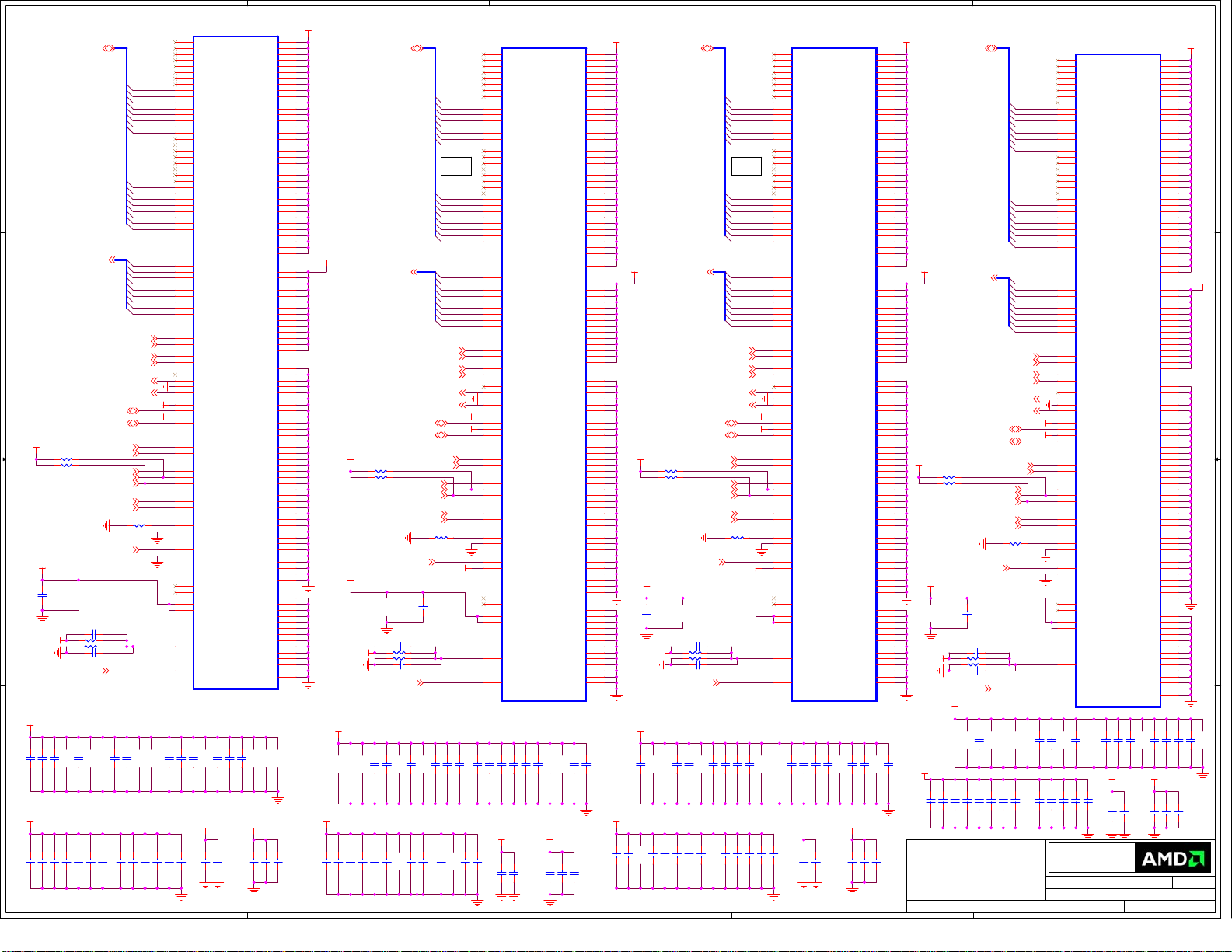
PCI-EXPRESS EDGE CONNECTOR
D D
+3.3V_BUS
GPIO_4_SMBCLKp.6
GPIO_3_SMBDATAp.6
Place these caps as close to the PCIE
connector as possible
+12V_BUS
C C
CAP CER 10UF 20% 16V X5R
(1206)1.8MM H MAX
+12V_BUS
C152
C152
C151
C151
150nF_16V
150nF_16V
150nF_16V
150nF_16V
+3.3V_BUS
CAP CER 10UF 10% 6.3V X5R
(0805)1.4MM MAX THICK
+3.3V_BUS
C155
C155
C156
1uF_6.3V
1uF_6.3V
C156
10nF
10nF
C154
C154
100nF_6.3V
100nF_6.3V
B B
+3.3V_BUS
DNIDNI
+3.3V_BUS
+3.3V_BUS
PETn0_GFXRn0p.2
PETp1_GFXRp1p.2
PETn1_GFXRn1p.2
PETp2_GFXRp2p.2
PETn2_GFXRn2p.2
PETp3_GFXRp3p.2
PETn3_GFXRn3p.2
PETp4_GFXRp4p.2
PETn4_GFXRn4p.2
PETp5_GFXRp5p.2
PETn5_GFXRn5p.2
PETp6_GFXRp6p.2
PETn6_GFXRn6p.2
PETp7_GFXRp7p.2
PETn7_GFXRn7p.2
PETp8_GFXRp8p.2
PETn8_GFXRn8p.2
PETp9_GFXRp9p.2
PETn9_GFXRn9p.2
PETp10_GFXRp10p.2
PETn10_GFXRn10p.2
PETp11_GFXRp11p.2
PETn11_GFXRn11p.2
PETp12_GFXRp12p.2
PETn12_GFXRn12p.2
PETp13_GFXRp13p.2
PETn13_GFXRn13p.2
PETp14_GFXRp14p.2
PETn14_GFXRn14p.2
PETp15_GFXRp15p.2
PETn15_GFXRn15p.2
DNI
DNI
PRESENCE
+3.3V_BUS
SMCLK
+12V_BUS
B1
B2
B3
B4
B5
B6
B7
B8
B9
B10
B11
B12
B13
B14
B15
B16
B17
B18
B19
B20
B21
B22
B23
B24
B25
B26
B27
B28
B29
B30
B31
B32
B33
B34
B35
B36
B37
B38
B39
B40
B41
B42
B43
B44
B45
B46
B47
B48
B49
B50
B51
B52
B53
B54
B55
B56
B57
B58
B59
B60
B61
B62
B63
B64
B65
B66
B67
B68
B69
B70
B71
B72
B73
B74
B75
B76
B77
B78
B79
B80
B81
B82
+12V#B1
+12V#B2
+12V#B3
GND#B4
SMCLK
SMDAT
GND#B7
+3.3V#B8
JTAG1
3.3Vaux
WAKE#
RSVD#B12
GND#B13
PETp0
PETn0
GND#B16
PRSNT2#B17
GND#B18
PETp1
PETn1
GND#B21
GND#B22
PETp2
PETn2
GND#B25
GND#B26
PETp3
PETn3
GND#B29
RSVD#B30
PRSNT2#B31
GND#B32
PETp4
PETn4
GND#B35
GND#B36
PETp5
PETn5
GND#B39
GND#B40
PETp6
PETn6
GND#B43
GND#B44
PETp7
PETn7
GND#B47
PRSNT2#B48
GND#B49
PETp8
PETn8
GND#B52
GND#B53
PETp9
PETn9
GND#B56
GND#B57
PETp10
PETn10
GND#B60
GND#B61
PETp11
PETn11
GND#B64
GND#B65
PETp12
PETn12
GND#B68
GND#B69
PETp13
PETn13
GND#B72
GND#B73
PETp14
PETn14
GND#B76
GND#B77
PETp15
PETn15
GND#B80
PRSNT2#B81
RSVD#B82
x16 PCIe
x16 PCIe
Mechanical Key
Mechanical Key
MPCIE100
MPCIE100
PRSNT1#A1
+12V#A2
+12V#A3
GND#A4
JTAG2
JTAG3
JTAG4
JTAG5
+3.3V#A9
+3.3V#A10
PERST#
GND#A12
REFCLK+
REFCLKGND#A15
PERp0
PERn0
GND#A18
RSVD#A19
GND#A20
PERp1
PERn1
GND#A23
GND#A24
PERp2
PERn2
GND#A27
GND#A28
PERp3
PERn3
GND#A31
RSVD#A32
RSVD#A33
GND#A34
PERp4
PERn4
GND#A37
GND#A38
PERp5
PERn5
GND#A41
GND#A42
PERp6
PERn6
GND#A45
GND#A46
PERp7
PERn7
GND#A49
RSVD#A50
GND#A51
PERp8
PERn8
GND#A54
GND#A55
PERp9
PERn9
GND#A58
GND#A59
PERp10
PERn10
GND#A62
GND#A63
PERp11
PERn11
GND#A66
GND#A67
PERp12
PERn12
GND#A70
GND#A71
PERp13
PERn13
GND#A74
GND#A75
PERp14
PERn14
GND#A78
GND#A79
PERp15
PERn15
GND#A82
A1
A2
A3
A4
A5
A6
A7
A8
A9
A10
A11
A12
A13
A14
A15
A16
A17
A18
A19
A20
A21
A22
A23
A24
A25
A26
A27
A28
A29
A30
A31
A32
A33
A34
A35
A36
A37
A38
A39
A40
A41
A42
A43
A44
A45
A46
A47
A48
A49
A50
A51
A52
A53
A54
A55
A56
A57
A58
A59
A60
A61
A62
A63
A64
A65
A66
A67
A68
A69
A70
A71
A72
A73
A74
A75
A76
A77
A78
A79
A80
A81
A82
PRESENCE
+12V_BUS
+3.3V_BUS
PERp0
PERn0
PERp1
PERn1
PERp2
PERn2
PERp3
PERn3
PERp4
PERn4
PERp5
PERn5
PERp6
PERn6
PERp7
PERn7
PERp8
PERn8
PERp9
PERn9
PERp10
PERn10
PERp11
PERn11
PERp12
PERn12
PERp13
PERn13
PERp14
PERn14
PERp15
PERn15
JTDIO_LOOPSMDAT
PERST#
SystemJTAGTDIandTDOarehardwired.
seep.20forGPUJTAGconnection
PCIE_REFCLKP p.2
PCIE_REFCLKN p.2PETp0_GFXRp0p.2
PERp0 p.2
PERn0 p.2
PERp1 p.2
PERn1 p.2
PERp2 p.2
PERn2 p.2
PERp3 p.2
PERn3 p.2
PERp4 p.2
PERn4 p.2
PERp5 p.2
PERn5 p.2
PERp6 p.2
PERn6 p.2
PERp7 p.2
PERn7 p.2
PERp8 p.2
PERn8 p.2
PERp9 p.2
PERn9 p.2
PERp10 p.2
PERn10 p.2
PERp11 p.2
PERn11 p.2
PERp12 p.2
PERn12 p.2
PERp13 p.2
PERn13 p.2
PERp14 p.2
PERn14 p.2
PERp15 p.2
PERn15 p.2
PCIe RESET Buffered
+3.3V_BUS
R102
R102
10K
10K
53
1
NC7SZ08P5X_NL
1V_LDO_POKp.6,15,18
R103 0RR103 0R
Place R104 in U100
PERST#_gated
R110 7.5KR110 7.5K
JTAG_TRSTB
R111 7.5KR111 7.5K
DNI
PERST#_buf
R112 7.5KR112 7.5K
PERST#_gated
1V_LDO_POK
PERST#_buf TESTEN
2
9 8
C160
C160
100pF_50V
100pF_50V
5 6
C161
C161
100pF_50V
100pF_50V
C159 100nF_6.3VC159 100nF_6.3V
2 3
C162
C162
100pF_50V
100pF_50V
12 11
NC7SZ08P5X_NL
U100
U100
+3.3V_BUS
SYMBOL LEGEND
DO NOT
DNI
INSTALL
ACTIVE
#
LOW
DIGITAL
GROUND
ANALOG
GROUND
of
of
of
BUO BRING UP
ONLY
Doc No.
Doc No.
Doc No.
102-C01301-00
102-C01301-00
102-C01301-00
1
RevDate:
RevDate:
RevDate:
50
50
50
A A
CONFIDENTIAL & PROPRIETARY TO ADVANCED MICRO DEVICES INC.
CONFIDENTIAL & PROPRIETARY TO ADVANCED MICRO DEVICES INC.
CONFIDENTIAL & PROPRIETARY TO ADVANCED MICRO DEVICES INC.
© 2007 Advanced Micro Devices
© 2007 Advanced Micro Devices
© 2007 Advanced Micro Devices
This AMD Board schematic and design is the exclusive property of AMD,
This AMD Board schematic and design is the exclusive property of AMD,
This AMD Board schematic and design is the exclusive property of AMD,
and is provided only to entities under a non-disclosure agreement
and is provided only to entities under a non-disclosure agreement
and is provided only to entities under a non-disclosure agreement
with AMD for evaluation purposes. Further distribution or disclosure
with AMD for evaluation purposes. Further distribution or disclosure
with AMD for evaluation purposes. Further distribution or disclosure
is strictly prohibited. Use of this schematic and design for any purpose
is strictly prohibited. Use of this schematic and design for any purpose
is strictly prohibited. Use of this schematic and design for any purpose
other than evaluation requires a Board Technology License Agreement
other than evaluation requires a Board Technology License Agreement
other than evaluation requires a Board Technology License Agreement
with AMD. AMD makes no representations or warranties of any kind
with AMD. AMD makes no representations or warranties of any kind
with AMD. AMD makes no representations or warranties of any kind
regarding this schematic and design, including, not limited to,
regarding this schematic and design, including, not limited to,
regarding this schematic and design, including, not limited to,
any implied warranty of merchantibility or fitness for a particular
any implied warranty of merchantibility or fitness for a particular
any implied warranty of merchantibility or fitness for a particular
purpose, and disclaims responsibility forany consequences resulting
purpose, and disclaims responsibility forany consequences resulting
purpose, and disclaims responsibility forany consequences resulting
from use of the information included herein.
from use of the information included herein.
from use of the information included herein.
Title
Title
Title
RH JUNIPER GDDR5 1GB DP+DP/HDMI+DVI /sVGA
RH JUNIPER GDDR5 1GB DP+DP/HDMI+DVI /sVGA
8
7
6
5
4
3
RH JUNIPER GDDR5 1GB DP+DP/HDMI+DVI /sVGA
2
Advanced Micro Devices Inc.
Advanced Micro Devices Inc.
Advanced Micro Devices Inc.
1 Commerce Valley Drive East
1 Commerce Valley Drive East
1 Commerce Valley Drive East
Markham, Ontario
Markham, Ontario
Markham, Ontario
Tuesday, November 10, 2009
Tuesday, November 10, 2009
Tuesday, November 10, 2009
Sheet
Sheet
Sheet
121
121
121
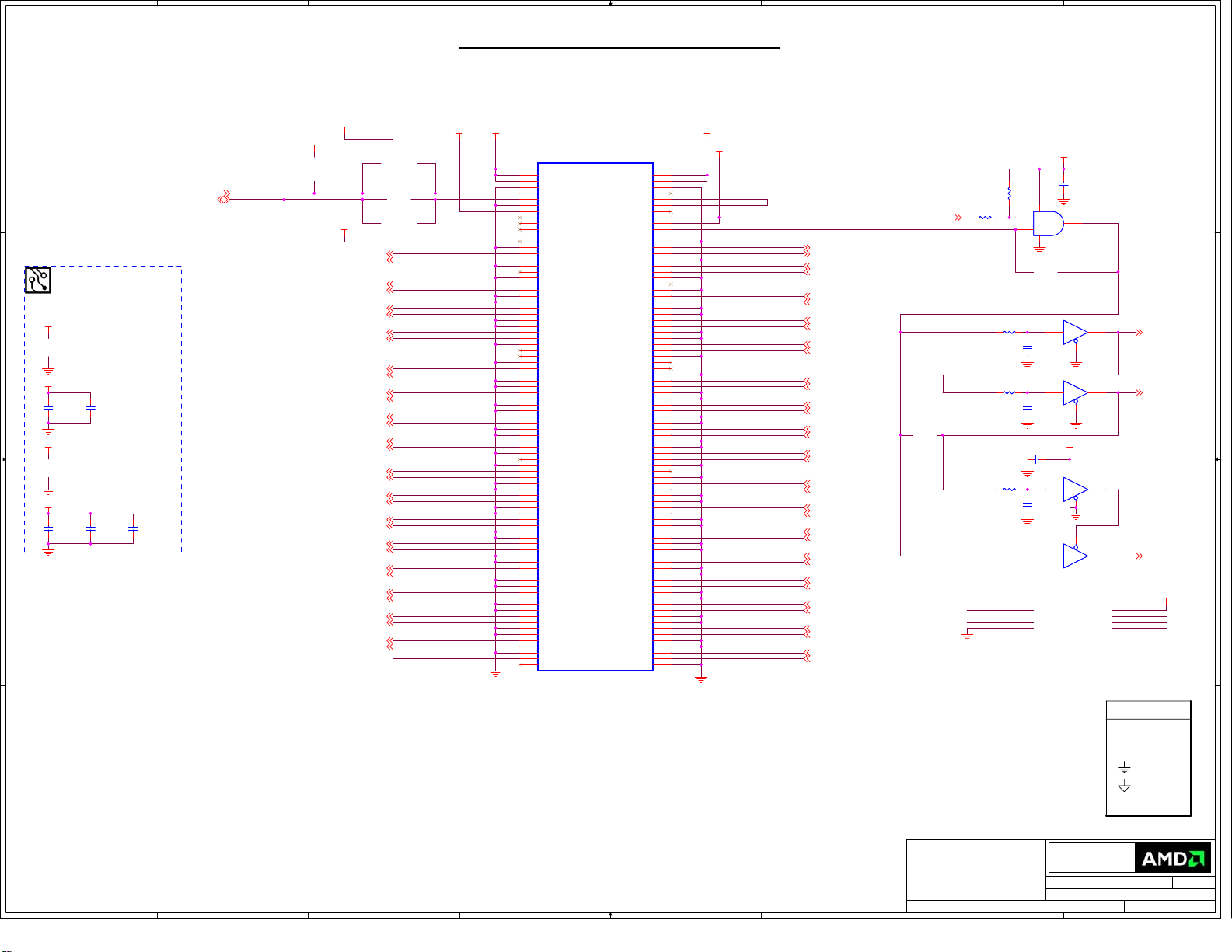
Page 2
5
4
3
2
1
(2) JUNIPER PCIe Interface
NOTE:SomeofthePCIEtestpointswill
beavailablethroughviasontraces.
C137
C137
TP105TP105
TP106TP106
TP107TP107
TP108TP108
TP113TP113
TP114TP114
TP115TP115
TP116TP116
TP121TP121
TP122TP122
C133
C133
1uF_6.3V
1uF_6.3V
C138
C138
1uF_6.3V
1uF_6.3V
C145
C145
1uF_6.3V
1uF_6.3V
TP101TP101
TP102TP102
TP103TP103
TP104TP104
TP109TP109
TP110TP110
TP111TP111
TP112TP112
TP117TP117
TP118TP118
TP119TP119
TP120TP120
100nF_6.3V
100nF_6.3V
C134
C134
100nF_6.3V
100nF_6.3V
C139
C139
C146
C146
1uF_6.3V
1uF_6.3V
C135
C135
10nF
10nF
C140
C140
100nF_6.3V
100nF_6.3V
C147
C147
1uF_6.3V
1uF_6.3V
PETp0_GFXRp0p.1
PETn0_GFXRn0p.1
PETp1_GFXRp1p.1
PETn1_GFXRn1p.1
D D
C C
+1.8V
+1.8V
+1V
B B
PETp2_GFXRp2p.1
PETn2_GFXRn2p.1
PETp3_GFXRp3p.1
PETn3_GFXRn3p.1
PETp4_GFXRp4p.1
PETn4_GFXRn4p.1
PETp5_GFXRp5p.1
PETn5_GFXRn5p.1
PETp6_GFXRp6p.1
PETn6_GFXRn6p.1
PETp7_GFXRp7p.1
PETn7_GFXRn7p.1
PETp8_GFXRp8p.1
PETn8_GFXRn8p.1
PETp9_GFXRp9p.1
PETn9_GFXRn9p.1
PETp10_GFXRp10p.1
PETn10_GFXRn10p.1
PETp11_GFXRp11p.1
PETn11_GFXRn11p.1
PETp12_GFXRp12p.1
PETn12_GFXRn12p.1
PETp13_GFXRp13p.1
PETn13_GFXRn13p.1
PETp14_GFXRp14p.1
PETn14_GFXRn14p.1
PETp15_GFXRp15p.1
PETn15_GFXRn15p.1
PCIE_REFCLKPp.1
PCIE_REFCLKNp.1
B100 BLM15AG121SN1DB100 BLM15AG121SN1D
C141
C141
4.7uF_6.3V
4.7uF_6.3V
1uF_6.3V
1uF_6.3V
C148
C148
10uF
10uF
C142
C142
PERST#_bufp.1,18
C149
C149
1uF_6.3V
1uF_6.3V
C143
C143
1uF_6.3V
1uF_6.3V
+PCIE_PVDD
1uF_6.3V
1uF_6.3V
C150
C150
1uF_6.3V
1uF_6.3V
C136
C136
C132
C132
10uF
10uF
1uF_6.3V
1uF_6.3V
1uF_6.3V
1uF_6.3V
C144
C144
U1B
U1B
PART 2 OF 15
AA38
AB35
AA36
AA30
AB37
AA31
AA32
AA33
AA34
Y37
Y35
W36
W38
V37
V35
U36
U38
T37
T35
R36
R38
P37
P35
N36
N38
M37
M35
L36
L38
K37
K35
J36
J38
H37
H35
G36
G38
F37
F35
E37
V28
W29
W30
Y31
G30
G31
H29
H30
J29
J30
L28
M28
N28
R28
T28
U28
PART 2 OF 15
PCIE_RX0P
PCIE_RX0N
PCIE_RX1P
PCIE_RX1N
PCIE_RX2P
PCIE_RX2N
PCIE_RX3P
PCIE_RX3N
PCIE_RX4P
PCIE_RX4N
PCIE_RX5P
PCIE_RX5N
PCIE_RX6P
PCIE_RX6N
PCIE_RX7P
PCIE_RX7N
PCIE_RX8P
PCIE_RX8N
PCIE_RX9P
PCIE_RX9N
PCIE_RX10P
PCIE_RX10N
PCIE_RX11P
PCIE_RX11N
PCIE_RX12P
PCIE_RX12N
PCIE_RX13P
PCIE_RX13N
PCIE_RX14P
PCIE_RX14N
PCIE_RX15P
PCIE_RX15N
PCIE_REFCLKP
PCIE_REFCLKN
PERSTB
PCIE_PVDD
PCIE_VDDR#1
PCIE_VDDR#2
PCIE_VDDR#3
PCIE_VDDR#4
PCIE_VDDR#5
PCIE_VDDR#6
PCIE_VDDR#7
PCIE_VDDR#8
PCIE_VDDC#1
PCIE_VDDC#2
PCIE_VDDC#3
PCIE_VDDC#4
PCIE_VDDC#5
PCIE_VDDC#6
PCIE_VDDC#7
PCIE_VDDC#8
PCIE_VDDC#9
PCIE_VDDC#10
PCIE_VDDC#11
PCIE_VDDC#12
JUNIPER XT A12 HF MVD SLT BIN1 TSMC FB12
JUNIPER XT A12 HF MVD SLT BIN1 TSMC FB12
P
P
C
C
I
I
E
E
X
X
P
P
R
R
E
E
S
S
S
S
PCIE_TX0P
PCIE_TX0N
PCIE_TX1P
PCIE_TX1N
PCIE_TX2P
PCIE_TX2N
PCIE_TX3P
PCIE_TX3N
PCIE_TX4P
PCIE_TX4N
PCIE_TX5P
PCIE_TX5N
PCIE_TX6P
PCIE_TX6N
PCIE_TX7P
PCIE_TX7N
PCIE_TX8P
PCIE_TX8N
PCIE_TX9P
PCIE_TX9N
PCIE_TX10P
PCIE_TX10N
PCIE_TX11P
PCIE_TX11N
PCIE_TX12P
PCIE_TX12N
PCIE_TX13P
PCIE_TX13N
PCIE_TX14P
PCIE_TX14N
PCIE_TX15P
PCIE_TX15N
PCIE_CALRP
PCIE_CALRN
PCIE_VSS#1
PCIE_VSS#2
PCIE_VSS#3
PCIE_VSS#4
PCIE_VSS#5
PCIE_VSS#6
PCIE_VSS#7
PCIE_VSS#8
PCIE_VSS#9
PCIE_VSS#10
PCIE_VSS#11
PCIE_VSS#12
PCIE_VSS#13
PCIE_VSS#14
PCIE_VSS#15
PCIE_VSS#16
PCIE_VSS#17
PCIE_VSS#18
PCIE_VSS#19
PCIE_VSS#20
PCIE_VSS#21
PCIE_VSS#22
PCIE_VSS#23
PCIE_VSS#24
PCIE_VSS#25
PCIE_VSS#26
PCIE_VSS#27
PCIE_VSS#28
PCIE_VSS#29
PCIE_VSS#30
PCIE_VSS#31
PCIE_VSS#32
PCIE_VSS#33
PCIE_VSS#34
PCIE_VSS#35
Y33
Y32
W33
W32
U33
U32
U30
U29
T33
T32
T30
T29
P33
P32
P30
P29
N33
N32
N30
N29
L33
L32
L30
L29
K33
K32
J33
J32
K30
K29
H33
H32
Y30
Y29
AB39
E39
F34
F39
G33
G34
H31
H34
H39
J31
J34
K31
K34
K39
L31
L34
M34
M39
N31
N34
P31
P34
P39
R34
T31
T34
T39
U31
U34
V34
V39
W31
W34
Y34
Y39
PCIE_TX0P
PCIE_TX0N
PCIE_TX1P
PCIE_TX1N
PCIE_TX2P
PCIE_TX2N
PCIE_TX3P
PCIE_TX3N
PCIE_TX4P
PCIE_TX4N
PCIE_TX5P
PCIE_TX5N
PCIE_TX6P
PCIE_TX6N
PCIE_TX7P
PCIE_TX7N
PCIE_TX8P
PCIE_TX8N
PCIE_TX9P
PCIE_TX9N
PCIE_TX10P
PCIE_TX10N
PCIE_TX11P
PCIE_TX11N
PCIE_TX12P
PCIE_TX12N
PCIE_TX13P
PCIE_TX13N
PCIE_TX14P
PCIE_TX14N
PCIE_TX15P
PCIE_TX15N
PCIE_CALRP
PCIE_CALRN
100nF_6.3V
100nF_6.3V
100nF_6.3V
100nF_6.3V
100nF_6.3V
100nF_6.3V
100nF_6.3V
100nF_6.3V
100nF_6.3V
100nF_6.3V
100nF_6.3V
100nF_6.3V
100nF_6.3V
100nF_6.3V
100nF_6.3V
100nF_6.3V
100nF_6.3V
100nF_6.3V
100nF_6.3V
100nF_6.3V
100nF_6.3V
100nF_6.3V
100nF_6.3V
100nF_6.3V
100nF_6.3V
100nF_6.3V
100nF_6.3V
100nF_6.3V
100nF_6.3V
100nF_6.3V
100nF_6.3V
100nF_6.3V
C100
C100
100nF_6.3V
100nF_6.3V
C102
C102
R1001.27K R1001.27K
R1012.0K R1012.0K
C104
C104
C106
C106
C108
C108
C111
C111
C112
C112
C114
C114
C116
C116
C118
C118
C120
C120
C122
C122
C124
C124
C126
C126
C128
C128
C130
C130
C101
C101
C103
C103
100nF_6.3V
100nF_6.3V
C105
C105
100nF_6.3V
100nF_6.3V
C107
C107
100nF_6.3V
100nF_6.3V
C110
C110
100nF_6.3V
100nF_6.3V
C109
C109
100nF_6.3V
100nF_6.3V
C113
C113
100nF_6.3V
100nF_6.3V
C115
C115
100nF_6.3V
100nF_6.3V
C117
C117
100nF_6.3V
100nF_6.3V
C119
C119
100nF_6.3V
100nF_6.3V
C121
C121
100nF_6.3V
100nF_6.3V
C123
C123
100nF_6.3V
100nF_6.3V
C125
C125
100nF_6.3V
100nF_6.3V
C127
C127
100nF_6.3V
100nF_6.3V
C129
C129
100nF_6.3V
100nF_6.3V
C131
C131
100nF_6.3V
100nF_6.3V
+1V
PERp0 p.1
PERn0 p.1
PERp1 p.1
PERn1 p.1
PERp2 p.1
PERn2 p.1
PERp3 p.1
PERn3 p.1
PERp4 p.1
PERn4 p.1
PERp5 p.1
PERn5 p.1
PERp6 p.1
PERn6 p.1
PERp7 p.1
PERn7 p.1
PERp8 p.1
PERn8 p.1
PERp9 p.1
PERn9 p.1
PERp10 p.1
PERn10 p.1
PERp11 p.1
PERn11 p.1
PERp12 p.1
PERn12 p.1
PERp13 p.1
PERn13 p.1
PERp14 p.1
PERn14 p.1
PERp15 p.1
PERn15 p.1
A A
CONFIDENTIAL & PROPRIETARY TO ADVANCED MICRO DEVICES INC.
CONFIDENTIAL & PROPRIETARY TO ADVANCED MICRO DEVICES INC.
CONFIDENTIAL & PROPRIETARY TO ADVANCED MICRO DEVICES INC.
© 2007 Advanced Micro Devices
© 2007 Advanced Micro Devices
© 2007 Advanced Micro Devices
This AMD Board schematic and design is the exclusive property of AMD,
This AMD Board schematic and design is the exclusive property of AMD,
This AMD Board schematic and design is the exclusive property of AMD,
and is provided only to entities under a non-disclosure agreement
and is provided only to entities under a non-disclosure agreement
and is provided only to entities under a non-disclosure agreement
with AMD for evaluation purposes. Further distribution or disclosure
with AMD for evaluation purposes. Further distribution or disclosure
with AMD for evaluation purposes. Further distribution or disclosure
is strictly prohibited. Use of this schematic and design for any purpose
is strictly prohibited. Use of this schematic and design for any purpose
is strictly prohibited. Use of this schematic and design for any purpose
other than evaluation requires a Board Technology License Agreement
other than evaluation requires a Board Technology License Agreement
other than evaluation requires a Board Technology License Agreement
with AMD. AMD makes no representations or warranties of any kind
with AMD. AMD makes no representations or warranties of any kind
with AMD. AMD makes no representations or warranties of any kind
regarding this schematic and design, including, not limited to,
regarding this schematic and design, including, not limited to,
regarding this schematic and design, including, not limited to,
any implied warranty of merchantibility or fitness for a particular
any implied warranty of merchantibility or fitness for a particular
any implied warranty of merchantibility or fitness for a particular
purpose, and disclaims responsibility forany consequences resulting
purpose, and disclaims responsibility forany consequences resulting
purpose, and disclaims responsibility forany consequences resulting
from use of the information included herein.
from use of the information included herein.
from use of the information included herein.
Title
Title
Title
RH JUNIPER GDDR5 1GB DP+DP/HDMI+DVI /sVGA
RH JUNIPER GDDR5 1GB DP+DP/HDMI+DVI /sVGA
5
4
3
2
RH JUNIPER GDDR5 1GB DP+DP/HDMI+DVI /sVGA
Advanced Micro Devices Inc.
Advanced Micro Devices Inc.
Advanced Micro Devices Inc.
1 Commerce Valley Drive East
1 Commerce Valley Drive East
1 Commerce Valley Drive East
Markham, Ontario
Markham, Ontario
Markham, Ontario
Tuesday, November 10, 2009
Tuesday, November 10, 2009
Tuesday, November 10, 2009
Sheet
Sheet
Sheet
of
221
of
221
of
221
1
Doc No.
Doc No.
Doc No.
RevDate:
RevDate:
RevDate:
50
50
50
102-C01301-00
102-C01301-00
102-C01301-00
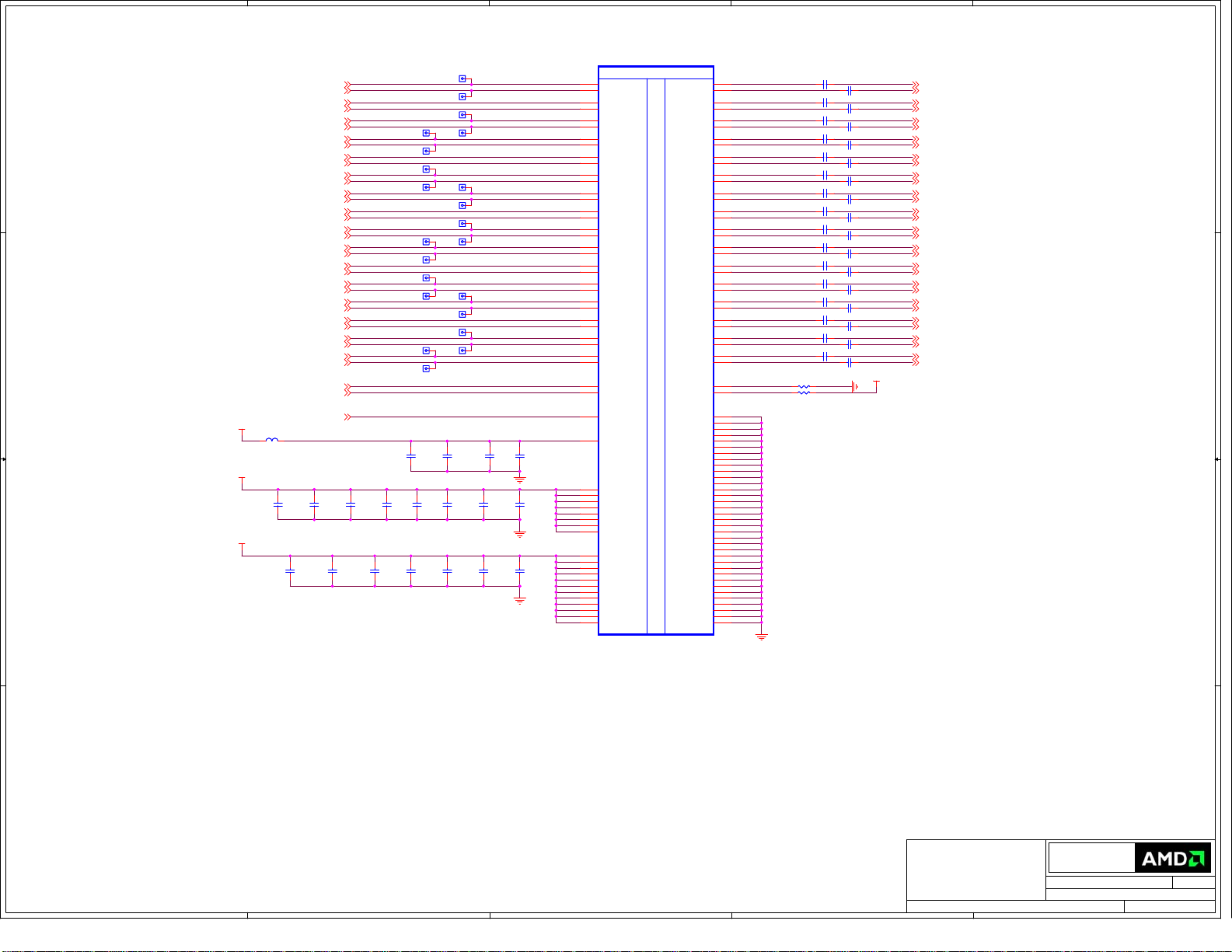
Page 3
5
4
3
2
1
(3) JUNIPER MEM Interface Ch A&B
U1C
U1C
D D
MAA0_[8..0]p.4
C C
WCKA0_0p.4
WCKA0b_0p.4
WCKA0_1p.4
WCKA0b_1p.4
EDCA0_0p.4
EDCA0_1p.4
EDCA0_2p.4
EDCA0_3p.4
DDBIA0_0p.4
DDBIA0_1p.4
DDBIA0_2p.4
DDBIA0_3p.4
ADBIA0p.4
B B
DQA0_0
DQA0_1
DQA0_2
DQA0_3
DQA0_4
DQA0_5
DQA0_6
DQA0_7
DQA0_8
DQA0_9
DQA0_10
DQA0_11
DQA0_12
DQA0_13
DQA0_14
DQA0_15
DQA0_16
DQA0_17
DQA0_18
DQA0_19
DQA0_20
DQA0_21
DQA0_22
DQA0_23
DQA0_24
DQA0_25
DQA0_26
DQA0_27
DQA0_28
DQA0_29
DQA0_30
DQA0_31
MAA0_0
MAA0_1
MAA0_2
MAA0_3
MAA0_4
MAA0_5
MAA0_6
MAA0_7
MAA0_8
CSA0b_0p.4
CASA0bp.4
RASA0bp.4
WEA0bp.4
CKEA0p.4
CLKA0p.4
CLKA0bp.4
C37
DQA0_0
C35
DQA0_1
A35
DQA0_2
E34
DQA0_3
G32
DQA0_4
D33
DQA0_5
F32
DQA0_6
E32
DQA0_7
D31
DQA0_8
F30
DQA0_9
C30
DQA0_10
A30
DQA0_11
F28
DQA0_12
C28
DQA0_13
A28
DQA0_14
E28
DQA0_15
D27
DQA0_16
F26
DQA0_17
C26
DQA0_18
A26
DQA0_19
F24
DQA0_20
C24
DQA0_21
A24
DQA0_22
E24
DQA0_23
C22
DQA0_24
A22
DQA0_25
F22
DQA0_26
D21
DQA0_27
A20
DQA0_28
F20
DQA0_29
D19
DQA0_30
E18
DQA0_31
G24
MAA0_0
J23
MAA0_1
H24
MAA0_2
J24
MAA0_3
H26
MAA0_4
J26
MAA0_5
H21
MAA0_6
G21
MAA0_7
H23
MAA0_8
A32
WCKA0_0
C32
WCKA0B_0
D23
WCKA0_1
E22
WCKA0B_1
C34
EDCA0_0
D29
EDCA0_1
D25
EDCA0_2
E20
EDCA0_3
A34
DDBIA0_0
E30
DDBIA0_1
E26
DDBIA0_2
C20
DDBIA0_3
J21
ADBIA0
K24
CSA0B_0
K27
CSA0B_1
K20
CASA0B
K23
RASA0B
K26
WEA0B
K21
CKEA0
H27
CLKA0
G27
CLKA0B
PART 3 OF 15
PART 3 OF 15
M
M
E
E
M
M
O
O
R
R
Y
Y
I
I
N
N
T
T
E
E
R
R
F
F
A
A
C
C
E
E
B
B
A
A
N
N
K
K
A
A
DQA1_0
DQA1_1
DQA1_2
DQA1_3
DQA1_4
DQA1_5
DQA1_6
DQA1_7
DQA1_8
DQA1_9
DQA1_10
DQA1_11
DQA1_12
DQA1_13
DQA1_14
DQA1_15
DQA1_16
DQA1_17
DQA1_18
DQA1_19
DQA1_20
DQA1_21
DQA1_22
DQA1_23
DQA1_24
DQA1_25
DQA1_26
DQA1_27
DQA1_28
DQA1_29
DQA1_30
DQA1_31
MAA1_0
MAA1_1
MAA1_2
MAA1_3
MAA1_4
MAA1_5
MAA1_6
MAA1_7
MAA1_8
WCKA1_0
WCKA1B_0
WCKA1_1
WCKA1B_1
EDCA1_0
EDCA1_1
EDCA1_2
EDCA1_3
DDBIA1_0
DDBIA1_1
DDBIA1_2
DDBIA1_3
ADBIA1
CSA1B_0
CSA1B_1
CASA1B
RASA1B
WEA1B
CKEA1
CLKA1
CLKA1B
C18
DQA1_0
A18
DQA1_1
F18
DQA1_2
D17
DQA1_3
A16
DQA1_4
F16
DQA1_5
D15
DQA1_6
E14
DQA1_7
F14
DQA1_8
D13
DQA1_9
F12
DQA1_10
A12
DQA1_11
D11
DQA1_12
F10
DQA1_13
A10
DQA1_14
C10
DQA1_15
G13
DQA1_16
H13
DQA1_17
J13
DQA1_18
H11
DQA1_19
G10
DQA1_20
G8
DQA1_21
K9
DQA1_22
K10
DQA1_23
G9
DQA1_24
A8
DQA1_25
C8
DQA1_26
E8
DQA1_27
A6
DQA1_28
C6
DQA1_29
E6
DQA1_30
A5
DQA1_31
H19
MAA1_0
H20
MAA1_1
L13
MAA1_2
G16
MAA1_3
J16
MAA1_4
H16
MAA1_5
J17
MAA1_6
H17
MAA1_7
J19
MAA1_8
C14
A14
E10
D9
E16
E12
J10
D7
C16
C12
J11
F8
G19
M13
K16
K17
K19
L15
J20
J14
H14
DQA1_[31..0] p.4DQA0_[31..0]p.4 DQB0_[31..0]p.5 DQB1_[31..0] p.5
MAA1_[8..0] p.4
WCKA1_0 p.4
WCKA1b_0 p.4
WCKA1_1 p.4
WCKA1b_1 p.4
EDCA1_0 p.4
EDCA1_1 p.4
EDCA1_2 p.4
EDCA1_3 p.4
DDBIA1_0 p.4
DDBIA1_1 p.4
DDBIA1_2 p.4
DDBIA1_3 p.4
ADBIA1 p.4
CSA1b_0 p.4
CASA1b p.4
RASA1b p.4
WEA1b p.4
CKEA1 p.4
CLKA1 p.4
CLKA1b p.4
+MVDD
MAB0_[8..0]p.5
WCKB0_0p.5
WCKB0b_0p.5
WCKB0_1p.5
WCKB0b_1p.5
EDCB0_0p.5
EDCB0_1p.5
EDCB0_2p.5
EDCB0_3p.5
DDBIB0_0p.5
DDBIB0_1p.5
DDBIB0_2p.5
DDBIB0_3p.5
ADBIB0p.5
DQB0_0
DQB0_1
DQB0_2
DQB0_3
DQB0_4
DQB0_5
DQB0_6
DQB0_7
DQB0_8
DQB0_9
DQB0_10
DQB0_11
DQB0_12
DQB0_13
DQB0_14
DQB0_15
DQB0_16
DQB0_17
DQB0_18
DQB0_19
DQB0_20
DQB0_21
DQB0_22
DQB0_23
DQB0_24
DQB0_25
DQB0_26
DQB0_27
DQB0_28
DQB0_29
DQB0_30
DQB0_31
MAB0_0
MAB0_1
MAB0_2
MAB0_3
MAB0_4
MAB0_5
MAB0_6
MAB0_7
MAB0_8
CSB0b_0p.5
CASB0bp.5
RASB0bp.5
WEB0bp.5
CKEB0p.5
CLKB0p.5
CLKB0bp.5
U1D
U1D
C5
DQB0_0
C3
DQB0_1
E3
DQB0_2
E1
DQB0_3
F1
DQB0_4
F3
DQB0_5
F5
DQB0_6
G4
DQB0_7
H5
DQB0_8
H6
DQB0_9
J4
DQB0_10
K6
DQB0_11
K5
DQB0_12
L4
DQB0_13
M6
DQB0_14
M1
DQB0_15
M3
DQB0_16
M5
DQB0_17
N4
DQB0_18
P6
DQB0_19
P5
DQB0_20
R4
DQB0_21
T6
DQB0_22
T1
DQB0_23
U4
DQB0_24
V6
DQB0_25
V1
DQB0_26
V3
DQB0_27
Y6
DQB0_28
Y1
DQB0_29
Y3
DQB0_30
Y5
DQB0_31
P8
MAB0_0
T9
MAB0_1
P9
MAB0_2
N7
MAB0_3
N8
MAB0_4
N9
MAB0_5
U9
MAB0_6
U8
MAB0_7
T8
MAB0_8
H3
WCKB0_0
H1
WCKB0B_0
T3
WCKB0_1
T5
WCKB0B_1
F6
EDCB0_0
K3
EDCB0_1
P3
EDCB0_2
V5
EDCB0_3
G7
DDBIB0_0
K1
DDBIB0_1
P1
DDBIB0_2
W4
DDBIB0_3
T7
ADBIB0
P10
CSB0B_0
L10
CSB0B_1
W10
CASB0B
T10
RASB0B
N10
WEB0B
U10
CKEB0
L9
CLKB0
L8
CLKB0B
PART 4 OF 15
PART 4 OF 15
M
M
E
E
M
M
O
O
R
R
Y
Y
I
I
N
N
T
T
E
E
R
R
F
F
A
A
C
C
E
E
B
B
A
A
N
N
K
K
B
B
DQB1_0
DQB1_1
DQB1_2
DQB1_3
DQB1_4
DQB1_5
DQB1_6
DQB1_7
DQB1_8
DQB1_9
DQB1_10
DQB1_11
DQB1_12
DQB1_13
DQB1_14
DQB1_15
DQB1_16
DQB1_17
DQB1_18
DQB1_19
DQB1_20
DQB1_21
DQB1_22
DQB1_23
DQB1_24
DQB1_25
DQB1_26
DQB1_27
DQB1_28
DQB1_29
DQB1_30
DQB1_31
MAB1_0
MAB1_1
MAB1_2
MAB1_3
MAB1_4
MAB1_5
MAB1_6
MAB1_7
MAB1_8
WCKB1_0
WCKB1B_0
WCKB1_1
WCKB1B_1
EDCB1_0
EDCB1_1
EDCB1_2
EDCB1_3
DDBIB1_0
DDBIB1_1
DDBIB1_2
DDBIB1_3
ADBIB1
CSB1B_0
CSB1B_1
CASB1B
RASB1B
WEB1B
CKEB1
CLKB1
CLKB1B
AA4
AB6
AB1
AB3
AD6
AD1
AD3
AD5
AF1
AF3
AF6
AG4
AH5
AH6
AJ4
AK3
AF8
AF9
AG8
AG7
AK9
AL7
AM8
AM7
AK1
AL4
AM6
AM1
AN4
AP3
AP1
AP5
Y9
W9
AC8
AC9
AA7
AA8
Y8
AA9
W8
AE4
AF5
AK6
AK5
AB5
AH1
AJ9
AM5
AC4
AH3
AJ8
AM3
W7
AD10
AC10
AA10
Y10
AB11
AA11
AD8
AD7
DQB1_0
DQB1_1
DQB1_2
DQB1_3
DQB1_4
DQB1_5
DQB1_6
DQB1_7
DQB1_8
DQB1_9
DQB1_10
DQB1_11
DQB1_12
DQB1_13
DQB1_14
DQB1_15
DQB1_16
DQB1_17
DQB1_18
DQB1_19
DQB1_20
DQB1_21
DQB1_22
DQB1_23
DQB1_24
DQB1_25
DQB1_26
DQB1_27
DQB1_28
DQB1_29
DQB1_30
DQB1_31
MAB1_0
MAB1_1
MAB1_2
MAB1_3
MAB1_4
MAB1_5
MAB1_6
MAB1_7
MAB1_8
MAB1_[8..0] p.5
WCKB1_0 p.5
WCKB1b_0 p.5
WCKB1_1 p.5
WCKB1b_1 p.5
EDCB1_0 p.5
EDCB1_1 p.5
EDCB1_2 p.5
EDCB1_3 p.5
DDBIB1_0 p.5
DDBIB1_1 p.5
DDBIB1_2 p.5
DDBIB1_3 p.5
ADBIB1 p.5
CSB1b_0 p.5
CASB1b p.5
RASB1b p.5
WEB1b p.5
CKEB1 p.5
CLKB1 p.5
CLKB1b p.5
+MVDD
R3605
R3605
40.2R
40.2R
C3603
C3603
1uF_6.3V
1uF_6.3V
1%
R3608
R3608
100R
100R
1%
C3606
C3606
1uF_6.3V
1uF_6.3V
+MVDD +MVDD
R3609
R3609
40.2R
40.2R
1%
R3611
R3611
100R
100R
1%
R3603243R R3603243R
R3604243R R3604243R
R3601243R R3601243R
R3602243R R3602243R
R3613243R R3613243R
R3614243R R3614243R
NOTFORPRODUCTION‐FORBACKUPONLY;
3
MEM_CALRP0
MEM_CALRN0
MEM_CALRP1
MEM_CALRN1
MEM_CALRP2
MEM_CALRN2
M27
MEM_CALRP0
L27
MEM_CALRN0
M12
MEM_CALRP1
N12
MEM_CALRN1
AH12
MEM_CALRP2
AG12
MEM_CALRN2
JUNIPER XT A12 HF MVD SLT BIN1 TSMC FB12
JUNIPER XT A12 HF MVD SLT BIN1 TSMC FB12
2
Y12
MVREFDB
MVREFSB
CONFIDENTIAL & PROPRIETARY TO ADVANCED MICRO DEVICES INC.
CONFIDENTIAL & PROPRIETARY TO ADVANCED MICRO DEVICES INC.
CONFIDENTIAL & PROPRIETARY TO ADVANCED MICRO DEVICES INC.
© 2007 Advanced Micro Devices
© 2007 Advanced Micro Devices
© 2007 Advanced Micro Devices
This AMD Board schematic and design is the exclusive property of AMD,
This AMD Board schematic and design is the exclusive property of AMD,
This AMD Board schematic and design is the exclusive property of AMD,
and is provided only to entities under a non-disclosure agreement
and is provided only to entities under a non-disclosure agreement
and is provided only to entities under a non-disclosure agreement
with AMD for evaluation purposes. Further distribution or disclosure
with AMD for evaluation purposes. Further distribution or disclosure
with AMD for evaluation purposes. Further distribution or disclosure
is strictly prohibited. Use of this schematic and design for any purpose
is strictly prohibited. Use of this schematic and design for any purpose
is strictly prohibited. Use of this schematic and design for any purpose
other than evaluation requires a Board Technology License Agreement
other than evaluation requires a Board Technology License Agreement
other than evaluation requires a Board Technology License Agreement
with AMD. AMD makes no representations or warranties of any kind
with AMD. AMD makes no representations or warranties of any kind
with AMD. AMD makes no representations or warranties of any kind
regarding this schematic and design, including, not limited to,
regarding this schematic and design, including, not limited to,
regarding this schematic and design, including, not limited to,
any implied warranty of merchantibility or fitness for a particular
any implied warranty of merchantibility or fitness for a particular
any implied warranty of merchantibility or fitness for a particular
purpose, and disclaims responsibility forany consequences resulting
purpose, and disclaims responsibility forany consequences resulting
purpose, and disclaims responsibility forany consequences resulting
from use of the information included herein.
from use of the information included herein.
from use of the information included herein.
Title
Title
Title
RH JUNIPER GDDR5 1GB DP+DP/HDMI+DVI /sVGA
RH JUNIPER GDDR5 1GB DP+DP/HDMI+DVI /sVGA
RH JUNIPER GDDR5 1GB DP+DP/HDMI+DVI /sVGA
MVREFD_B
MVREFD/S =0.7*
VDDR1
(GDDR3/4/5)
AA12
MVREFS_B
1uF_6.3V
1uF_6.3V
L18
MVREFDA
AH11
DRST
DRAM_RSTp.4,5
A A
R3615 51.1RR3615 51.1R
C3608
C3608
10K
10K
PLEASESEEBOMFORQUALIFIEDVALUES
5
DRAM_RST
R3600
R3600
JUNIPER XT A12 HF MVD SLT BIN1 TSMC FB12
JUNIPER XT A12 HF MVD SLT BIN1 TSMC FB12
120pF_50V
120pF_50V
MVREFSA
MVREFD_A
MVREFD/S =0.7*
VDDR1
(GDDR3/4/5)
L20
MVREFS_A
4
R3606
R3606
40.2R
40.2R
1%
R3607
R3607
C3602
C3602
100R
100R
1%
C3607
C3607
1uF_6.3V
1uF_6.3V
Advanced Micro Devices Inc.
Advanced Micro Devices Inc.
Advanced Micro Devices Inc.
1 Commerce Valley Drive East
1 Commerce Valley Drive East
1 Commerce Valley Drive East
Markham, Ontario
Markham, Ontario
Markham, Ontario
Tuesday, November 10, 2009
Tuesday, November 10, 2009
Tuesday, November 10, 2009
Sheet
Sheet
Sheet
of
321
of
321
of
321
+MVDD
R3610
R3610
40.2R
40.2R
1%
R3612
R3612
100R
100R
1%
RevDate:
RevDate:
RevDate:
50
50
50
Doc No.
Doc No.
Doc No.
102-C01301-00
102-C01301-00
1
102-C01301-00
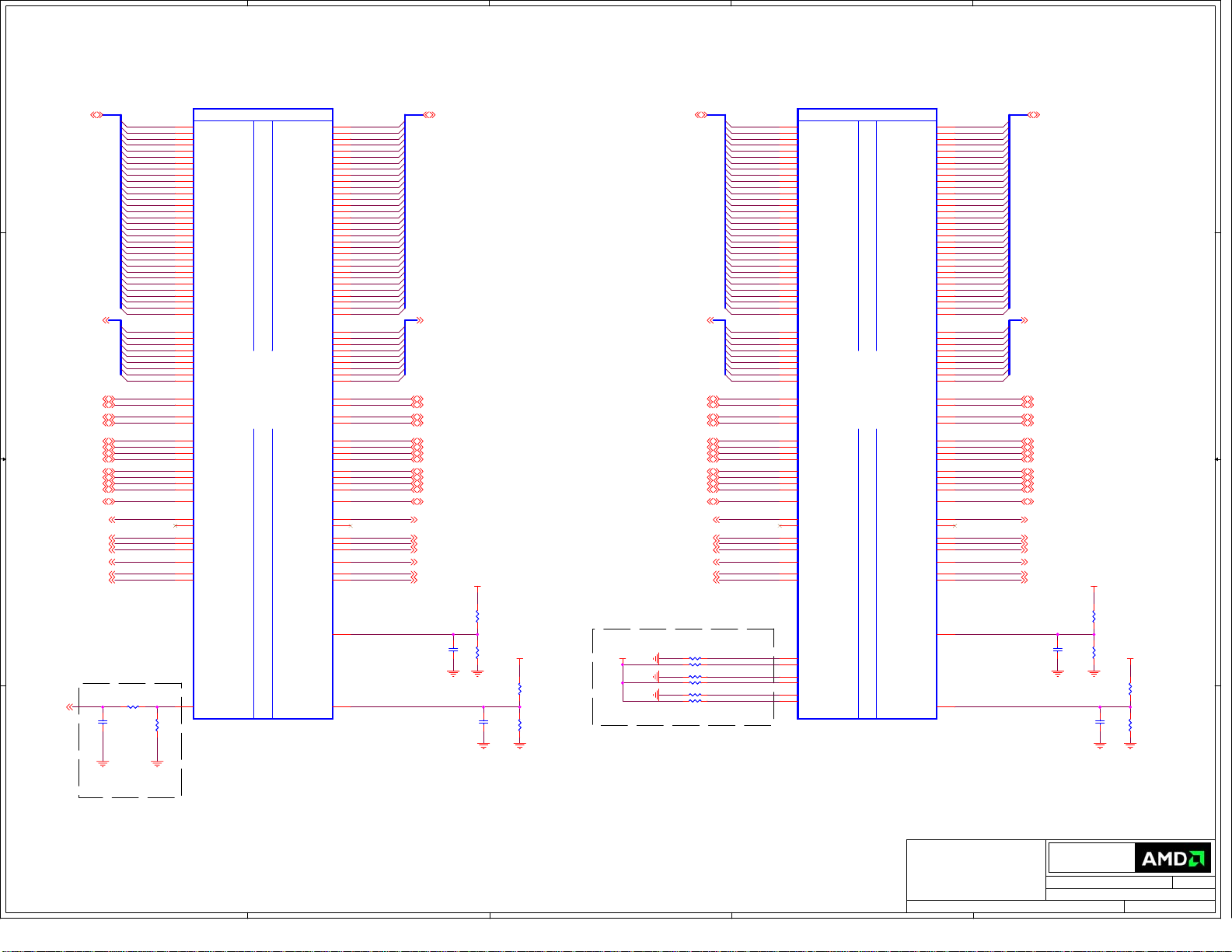
Page 4
5
(4) GDDR5 x16 MEM Channel A
VDD-C5
VDD-G1
VDD-G4
VDD-L1
VDD-L4
VDD-L11
VDD-L14
VDD-R5
VSS-B5
VSS-G5
VSS-H1
VSS-K1
VSS-L5
VSS-T5
VSS-T10
+MVDD
B1
B3
B12
B14
D1
D3
D12
D14
E5
E10
F1
F3
F12
F14
G2
G13
H3
H12
K3
K12
L2
L13
M1
M3
M12
M14
N5
N10
P1
P3
P12
P14
T1
T3
T12
T14
+MVDD
C5
C10
D11
G1
G4
G11
G14
L1
L4
L11
L14
P11
R5
R10
A1
A3
A12
A14
C1
C3
C4
C11
C12
C14
E1
E3
E12
E14
F5
F10
H2
H13
K2
K13
M5
M10
N1
N3
N12
N14
R1
R3
R4
R11
R12
R14
V1
V3
V12
V14
B5
B10
D10
G5
G10
H1
H14
K1
K14
L5
L10
P10
T5
T10
U2000
DQA0_[31..0]p.3
DQA0_17
DQA0_16
DQA0_18
D D
MAA0_[8..0]p.3
C C
+MVDD +MVDD +MVDD
R2003 120RR2003 120R
R2004 120RR2004 120R
DQA0_19
DQA0_20
DQA0_23
DQA0_21
DQA0_22
DQA0_10
DQA0_8
DQA0_11
DQA0_9
DQA0_12
DQA0_13
DQA0_14
DQA0_15
MAA0_8
MAA0_7
MAA0_6
MAA0_5
MAA0_4
MAA0_3
MAA0_2
MAA0_1
MAA0_0
WCKA0_0p.3
WCKA0b_0p.3
WCKA0_1p.3
WCKA0b_1p.3
EDCA0_2p.3
EDCA0_1p.3
+MVDD
DDBIA0_2p.3
+MVDD
DDBIA0_1p.3
RASA0bp.3
CASA0bp.3
CKEA0p.3
CLKA0bp.3
CLKA0p.3
CSA0b_0p.3
WEA0bp.3
R2002 120RR2002 120R
DRAM_RSTp.3,5
B B
+MEM_VREF +MEM_VREF
C2003
C2003
100nF_6.3V
100nF_6.3V
C2004 1uF_6.3VC2004 1uF_6.3V
1% 1%
R2009 2.37KR2009 2.37K
+MVDD +MVDD +MVDD
R2010 5.49KR2010 5.49K
C2005 1uF_6.3VC2005 1uF_6.3V
VREFC_A0 VREFC_B0
1%
ADBIA0p.3
U2000
M2
M4
N2
N4
T2
T4
V2
V4
M13
M11
N13
N11
T13
T11
V13
V11
F13
F11
E13
E11
B13
B11
A13
A11
F2
F4
E2
E4
B2
B4
A2
A4
J5
K4
K5
K10
K11
H10
H11
H5
H4
D4
D5
P4
P5
R2
R13
C13
C2
P2
P13
D13
D2
G3
L3
J3
J11
J12
G12
L12
J13
1%
J10
J2
J1
A5
V5
A10
V10
J14
J4
23F41GB7ME50
23F41GB7ME50
DQ31 | DQ7
DQ30 | DQ6
DQ29 | DQ5
DQ28 | DQ4
DQ27 | DQ3
DQ26 | DQ2
DQ25 | DQ1
DQ24 | DQ0
DQ23 | DQ15
DQ22 | DQ14
DQ21 | DQ13
DQ20 | DQ12
DQ19 | DQ11
DQ18 | DQ10
DQ17 | DQ9
DQ16 | DQ8
DQ15 | DQ23
DQ14 | DQ22
DQ13 | DQ21
DQ12 | DQ20
DQ11 | DQ19
DQ10 | DQ18
DQ9 | DQ17
DQ8 | DQ16
DQ7 | DQ31
DQ6 | DQ30
DQ5 | DQ29
DQ4 | DQ28
DQ3 | DQ27
DQ2 | DQ26
DQ1 | DQ25
DQ0 | DQ24
RFU/A12/NC
A7/A8 | A0/A10
A6/A11 | A1/A9
A5/BA1 | A3/BA3
A4/BA2 | A2/BA0
A3/BA3 | A5/BA1
A2 /BA0 | A4/BA2
A1/A9 | A6/A11
A0/A10 | A7/A8
WCK01 | WCK23
WCK01# | WCK23#
WCK23 | WCK01
WCK23# | WCK01#
EDC3 | EDC0
EDC2 | EDC1
EDC1 | EDC2
EDC0 | EDC3
DBI3# | DBI0#
DBI2 #| DBI1#
DBI1# | DBI2#
DBI0# | DBI3#
RAS# | CAS#
CAS# | RAS#
CKE#
CK#
CK
CS# | WE#
WE# | CS#
ZQ
SEN
RESET#
MF
Vpp,NC
Vpp,NC1
VREFD1
VREFD2
VREFC
ABI#
GDDR5
VDDQ-B1
VDDQ-B3
VDDQ-B12
VDDQ-B14
VDDQ-D1
VDDQ-D3
VDDQ-D12
VDDQ-D14
VDDQ-E5
VDDQ-E10
VDDQ-F1
VDDQ-F3
VDDQ-F12
VDDQ-F14
VDDQ-G2
VDDQ-G13
VDDQ-H3
VDDQ-H12
VDDQ-K3
VDDQ-K12
VDDQ-L2
VDDQ-L13
VDDQ-M1
VDDQ-M3
VDDQ-M12
VDDQ-M14
VDDQ-N5
VDDQ-N10
VDDQ-P1
VDDQ-P3
VDDQ-P12
VDDQ-P14
VDDQ-T1
VDDQ-T3
VDDQ-T12
VDDQ-T14
VDD-C10
VDD-D11
VDD-G11
VDD-G14
VDD-P11
VDD-R10
VSSQ-A1
VSSQ-A3
VSSQ-A12
VSSQ-A14
VSSQ-C1
VSSQ-C3
VSSQ-C4
VSSQ-C11
VSSQ-C12
VSSQ-C14
VSSQ-E1
VSSQ-E3
VSSQ-E12
VSSQ-E14
VSSQ-F5
VSSQ-F10
VSSQ-H2
VSSQ-H13
VSSQ-K2
VSSQ-K13
VSSQ-M5
VSSQ-M10
VSSQ-N1
VSSQ-N3
VSSQ-N12
VSSQ-N14
VSSQ-R1
VSSQ-R3
VSSQ-R4
VSSQ-R11
VSSQ-R12
VSSQ-R14
VSSQ-V1
VSSQ-V3
VSSQ-V12
VSSQ-V14
VSS-G10
VSS-B10
VSS-D10
VSS-H14
VSS-K14
VSS-L10
VSS-P10
4
CH_A0 =U2000 & U2100
DQA0_[31..0]p.3
MAA0_[8..0]p.3
R2103 120RR2103 120R
R2104 120RR2104 120R
DRAM_RSTp.3,5
C2139
C2139
100nF_6.3V
100nF_6.3V
C2138 1uF_6.3VC2138 1uF_6.3V
1% 1%
R2109 2.37KR2109 2.37K
R2110 5.49KR2110 5.49K
C2140 1uF_6.3VC2140 1uF_6.3V
ADBIA0p.3
DDBIA0_0p.3
DDBIA0_3p.3
CKEA0p.3
CLKA0bp.3
CLKA0p.3
R2101 120RR2101 120R
VREFC_A1
3
CH_A1 =U2200 & U2300
DQA1_15
DQA1_14
DQA1_13
DQA1_8
DQA1_12
DQA1_10
DQA1_11
DQA1_9
M=1
Mirror
DQA1_23
DQA1_22
DQA1_20
DQA1_21
DQA1_16
DQA1_18
DQA1_19
DQA1_17
MAA1_8
MAA1_0
MAA1_1
MAA1_3
MAA1_2
MAA1_5
MAA1_4
MAA1_6
MAA1_7
WCKA1_1p.3
WCKA1b_1p.3
WCKA1_0p.3
WCKA1b_0p.3
EDCA1_1p.3
EDCA1_2p.3
+MVDD
DDBIA1_1p.3 DDBIA1_0p.3
+MVDD
DDBIA1_2p.3
CASA1bp.3
RASA1bp.3
CKEA1p.3
CLKA1bp.3
CLKA1p.3
WEA1bp.3
CSA1b_0p.3
R2201 120RR2201 120R
DRAM_RSTp.3,5
+MVDD
C2242
C2242
100nF_6.3V
100nF_6.3V
1% 1%
1%
ADBIA1p.3
U2200
U2200
M2
DQ31 | DQ7
M4
DQ30 | DQ6
N2
DQ29 | DQ5
N4
DQ28 | DQ4
T2
DQ27 | DQ3
T4
DQ26 | DQ2
V2
DQ25 | DQ1
V4
DQ24 | DQ0
M13
DQ23 | DQ15
M11
DQ22 | DQ14
N13
DQ21 | DQ13
N11
DQ20 | DQ12
T13
DQ19 | DQ11
T11
DQ18 | DQ10
V13
DQ17 | DQ9
V11
DQ16 | DQ8
F13
DQ15 | DQ23
F11
DQ14 | DQ22
E13
DQ13 | DQ21
E11
DQ12 | DQ20
B13
DQ11 | DQ19
B11
DQ10 | DQ18
A13
DQ9 | DQ17
A11
DQ8 | DQ16
F2
DQ7 | DQ31
F4
DQ6 | DQ30
E2
DQ5 | DQ29
E4
DQ4 | DQ28
B2
DQ3 | DQ27
B4
DQ2 | DQ26
A2
DQ1 | DQ25
A4
DQ0 | DQ24
J5
RFU/A12/NC
K4
A7/A8 | A0/A10
K5
A6/A11 | A1/A9
K10
A5/BA1 | A3/BA3
K11
A4/BA2 | A2/BA0
H10
A3/BA3 | A5/BA1
H11
A2 /BA0 | A4/BA2
H5
A1/A9 | A6/A11
H4
A0/A10 | A7/A8
D4
WCK01 | WCK23
D5
WCK01# | WCK23#
P4
WCK23 | WCK01
P5
WCK23# | WCK01#
R2
EDC3 | EDC0
R13
EDC2 | EDC1
C13
EDC1 | EDC2
C2
EDC0 | EDC3
P2
DBI3# | DBI0#
P13
DBI2 #| DBI1#
D13
DBI1# | DBI2#
D2
DBI0# | DBI3#
G3
RAS# | CAS#
L3
CAS# | RAS#
J3
CKE#
J11
CK#
J12
CK
G12
CS# | WE#
L12
WE# | CS#
J13
1%
ZQ
J10
SEN
J2
RESET#
J1
MF
A5
Vpp,NC
V5
Vpp,NC1
A10
VREFD1
V10
VREFD2
J14
VREFC
J4
ABI#
23F41GB7ME50
23F41GB7ME50
VDD-C5
VDD-G1
VDD-G4
VDD-L1
VDD-L4
VDD-R5
VSS-B5
VSS-G5
VSS-H1
VSS-K1
VSS-L5
VSS-T5
+MVDD
B1
B3
B12
B14
D1
D3
D12
D14
E5
E10
F1
F3
F12
F14
G2
G13
H3
H12
K3
K12
L2
L13
M1
M3
M12
M14
N5
N10
P1
P3
P12
P14
T1
T3
T12
T14
C5
C10
D11
G1
G4
G11
G14
L1
L4
L11
L14
P11
R5
R10
A1
A3
A12
A14
C1
C3
C4
C11
C12
C14
E1
E3
E12
E14
F5
F10
H2
H13
K2
K13
M5
M10
N1
N3
N12
N14
R1
R3
R4
R11
R12
R14
V1
V3
V12
V14
B5
B10
D10
G5
G10
H1
H14
K1
K14
L5
L10
P10
T5
T10
+MVDD
DQA1_[31..0]p.3
R2203 120RR2203 120R
R2204 120RR2204 120R
+MEM_VREF
MAA1_[8..0]p.3
C2239 1uF_6.3VC2239 1uF_6.3V
R2209 2.37KR2209 2.37K
R2210 5.49KR2210 5.49K
C2241 1uF_6.3VC2241 1uF_6.3V
U2100
U2100
M2
M4
N2
N4
T2
T4
V2
V4
M13
DQA0_4
M11
DQA0_3
N13
DQA0_2
N11
DQA0_0
T13
DQA0_1
T11
DQA0_6
V13
DQA0_7
V11
DQA0_5
F13
F11
E13
M=1
E11
Mirror
B13
B11
A13
A11
+MVDD
+MVDD
F2
F4
E2
E4
B2
B4
A2
A4
J5
K4
K5
K10
K11
H10
H11
H5
H4
D4
D5
P4
P5
R2
R13
C13
C2
P2
P13
D13
D2
G3
L3
J3
J11
J12
G12
L12
J13
1%
J10
J2
J1
A5
V5
A10
V10
J14
DQA0_31
DQA0_29
DQA0_30
DQA0_28
DQA0_26
DQA0_25
DQA0_27
DQA0_24
MAA0_8
MAA0_0
MAA0_1
MAA0_3
MAA0_2
MAA0_5
MAA0_4
MAA0_6
MAA0_7
WCKA0_1p.3
WCKA0b_1p.3
WCKA0_0p.3
WCKA0b_0p.3
EDCA0_0p.3
EDCA0_3p.3
CASA0bp.3
RASA0bp.3
WEA0bp.3
CSA0b_0p.3
+MVDD
VREFC_A1
1%
J4
DQ31 | DQ7
DQ30 | DQ6
DQ29 | DQ5
DQ28 | DQ4
DQ27 | DQ3
DQ26 | DQ2
DQ25 | DQ1
DQ24 | DQ0
DQ23 | DQ15
DQ22 | DQ14
DQ21 | DQ13
DQ20 | DQ12
DQ19 | DQ11
DQ18 | DQ10
DQ17 | DQ9
DQ16 | DQ8
DQ15 | DQ23
DQ14 | DQ22
DQ13 | DQ21
DQ12 | DQ20
DQ11 | DQ19
DQ10 | DQ18
DQ9 | DQ17
DQ8 | DQ16
DQ7 | DQ31
DQ6 | DQ30
DQ5 | DQ29
DQ4 | DQ28
DQ3 | DQ27
DQ2 | DQ26
DQ1 | DQ25
DQ0 | DQ24
RFU/A12/NC
A7/A8 | A0/A10
A6/A11 | A1/A9
A5/BA1 | A3/BA3
A4/BA2 | A2/BA0
A3/BA3 | A5/BA1
A2 /BA0 | A4/BA2
A1/A9 | A6/A11
A0/A10 | A7/A8
WCK01 | WCK23
WCK01# | WCK23#
WCK23 | WCK01
WCK23# | WCK01#
EDC3 | EDC0
EDC2 | EDC1
EDC1 | EDC2
EDC0 | EDC3
DBI3# | DBI0#
DBI2 #| DBI1#
DBI1# | DBI2#
DBI0# | DBI3#
RAS# | CAS#
CAS# | RAS#
CKE#
CK#
CK
CS# | WE#
WE# | CS#
ZQ
SEN
RESET#
MF
Vpp,NC
Vpp,NC1
VREFD1
VREFD2
VREFC
ABI#
23F41GB7ME50
23F41GB7ME50
GDDR5
VDDQ-B1
VDDQ-B3
VDDQ-B12
VDDQ-B14
VDDQ-D1
VDDQ-D3
VDDQ-D12
VDDQ-D14
VDDQ-E5
VDDQ-E10
VDDQ-F1
VDDQ-F3
VDDQ-F12
VDDQ-F14
VDDQ-G2
VDDQ-G13
VDDQ-H3
VDDQ-H12
VDDQ-K3
VDDQ-K12
VDDQ-L2
VDDQ-L13
VDDQ-M1
VDDQ-M3
VDDQ-M12
VDDQ-M14
VDDQ-N5
VDDQ-N10
VDDQ-P1
VDDQ-P3
VDDQ-P12
VDDQ-P14
VDDQ-T1
VDDQ-T3
VDDQ-T12
VDDQ-T14
VDD-C10
VDD-D11
VDD-G11
VDD-G14
VDD-L11
VDD-L14
VDD-P11
VDD-R10
VSSQ-A1
VSSQ-A3
VSSQ-A12
VSSQ-A14
VSSQ-C1
VSSQ-C3
VSSQ-C4
VSSQ-C11
VSSQ-C12
VSSQ-C14
VSSQ-E1
VSSQ-E3
VSSQ-E12
VSSQ-E14
VSSQ-F5
VSSQ-F10
VSSQ-H2
VSSQ-H13
VSSQ-K2
VSSQ-K13
VSSQ-M5
VSSQ-M10
VSSQ-N1
VSSQ-N3
VSSQ-N12
VSSQ-N14
VSSQ-R1
VSSQ-R3
VSSQ-R4
VSSQ-R11
VSSQ-R12
VSSQ-R14
VSSQ-V1
VSSQ-V3
VSSQ-V12
VSSQ-V14
VSS-B10
VSS-D10
VSS-G10
VSS-H14
VSS-K14
VSS-L10
VSS-P10
VSS-T10
GDDR5
VDDQ-B1
VDDQ-B3
VDDQ-B12
VDDQ-B14
VDDQ-D1
VDDQ-D3
VDDQ-D12
VDDQ-D14
VDDQ-E5
VDDQ-E10
VDDQ-F1
VDDQ-F3
VDDQ-F12
VDDQ-F14
VDDQ-G2
VDDQ-G13
VDDQ-H3
VDDQ-H12
VDDQ-K3
VDDQ-K12
VDDQ-L2
VDDQ-L13
VDDQ-M1
VDDQ-M3
VDDQ-M12
VDDQ-M14
VDDQ-N5
VDDQ-N10
VDDQ-P1
VDDQ-P3
VDDQ-P12
VDDQ-P14
VDDQ-T1
VDDQ-T3
VDDQ-T12
VDDQ-T14
VDD-C5
VDD-C10
VDD-D11
VDD-G1
VDD-G4
VDD-G11
VDD-G14
VDD-L1
VDD-L4
VDD-L11
VDD-L14
VDD-P11
VDD-R5
VDD-R10
VSSQ-A1
VSSQ-A3
VSSQ-A12
VSSQ-A14
VSSQ-C1
VSSQ-C3
VSSQ-C4
VSSQ-C11
VSSQ-C12
VSSQ-C14
VSSQ-E1
VSSQ-E3
VSSQ-E12
VSSQ-E14
VSSQ-F5
VSSQ-F10
VSSQ-H2
VSSQ-H13
VSSQ-K2
VSSQ-K13
VSSQ-M5
VSSQ-M10
VSSQ-N1
VSSQ-N3
VSSQ-N12
VSSQ-N14
VSSQ-R1
VSSQ-R3
VSSQ-R4
VSSQ-R11
VSSQ-R12
VSSQ-R14
VSSQ-V1
VSSQ-V3
VSSQ-V12
VSSQ-V14
VSS-B5
VSS-B10
VSS-D10
VSS-G5
VSS-G10
VSS-H1
VSS-H14
VSS-K1
VSS-K14
VSS-L5
VSS-L10
VSS-P10
VSS-T5
VSS-T10
2
+MVDD
+MEM_VREF
+MVDD
+MVDD
R2305 120RR2305 120R
R2304 120RR2304 120R
C2344
C2344
100nF_6.3V
100nF_6.3V
+MVDD
DQA1_[31..0]p.3
MAA1_[8..0]p.3
DDBIA1_3p.3
DRAM_RSTp.3,5
C2343 1uF_6.3VC2343 1uF_6.3V
R2309 2.37KR2309 2.37K
R2310 5.49KR2310 5.49K
C2345 1uF_6.3VC2345 1uF_6.3V
ADBIA1p.3
C2305 1uF_6.3VC2305 1uF_6.3V
CLKA1bp.3
CLKA1p.3
CSA1b_0p.3
WEA1bp.3
C2306 1uF_6.3VC2306 1uF_6.3V
DQA1_26
DQA1_27
DQA1_28
DQA1_25
DQA1_24
DQA1_29
DQA1_30
DQA1_31
DQA1_1
DQA1_0
DQA1_2
DQA1_3
DQA1_4
DQA1_6
DQA1_5
DQA1_7
MAA1_8
MAA1_7
MAA1_6
MAA1_5
MAA1_4
MAA1_3
MAA1_2
MAA1_1
MAA1_0
WCKA1_0p.3
WCKA1b_0p.3
WCKA1_1p.3
WCKA1b_1p.3
EDCA1_3p.3
EDCA1_0p.3
+MVDD
+MVDD
RASA1bp.3
CASA1bp.3
CKEA1p.3
R2302 120RR2302 120R
1%
1%
C2308 1uF_6.3VC2308 1uF_6.3V
1%
VREFC_B1
+MVDD
B1
B3
B12
B14
D1
D3
D12
D14
E5
E10
F1
F3
F12
F14
G2
G13
H3
H12
K3
K12
L2
L13
M1
M3
M12
M14
N5
N10
P1
P3
P12
P14
T1
T3
T12
T14
C5
C10
D11
G1
G4
G11
G14
L1
L4
L11
L14
P11
R5
R10
A1
A3
A12
A14
C1
C3
C4
C11
C12
C14
E1
E3
E12
E14
F5
F10
H2
H13
K2
K13
M5
M10
N1
N3
N12
N14
R1
R3
R4
R11
R12
R14
V1
V3
V12
V14
B5
B10
D10
G5
G10
H1
H14
K1
K14
L5
L10
P10
T5
T10
U2300
U2300
M2
M4
N2
N4
M13
M11
N13
N11
T13
T11
V13
V11
F13
F11
E13
E11
B13
B11
A13
A11
K10
K11
H10
H11
H5
H4
D4
D5
R2
R13
C13
C2
P13
D13
D2
G3
J11
J12
G12
L12
J13
J10
A10
V10
J14
C2312 1uF_6.3VC2312 1uF_6.3V
DQ31 | DQ7
DQ30 | DQ6
DQ29 | DQ5
DQ28 | DQ4
T2
DQ27 | DQ3
T4
DQ26 | DQ2
V2
DQ25 | DQ1
V4
DQ24 | DQ0
DQ23 | DQ15
DQ22 | DQ14
DQ21 | DQ13
DQ20 | DQ12
DQ19 | DQ11
DQ18 | DQ10
DQ17 | DQ9
DQ16 | DQ8
DQ15 | DQ23
DQ14 | DQ22
DQ13 | DQ21
DQ12 | DQ20
DQ11 | DQ19
DQ10 | DQ18
DQ9 | DQ17
DQ8 | DQ16
F2
DQ7 | DQ31
F4
DQ6 | DQ30
E2
DQ5 | DQ29
E4
DQ4 | DQ28
B2
DQ3 | DQ27
B4
DQ2 | DQ26
A2
DQ1 | DQ25
A4
DQ0 | DQ24
J5
RFU/A12/NC
K4
A7/A8 | A0/A10
K5
A6/A11 | A1/A9
A5/BA1 | A3/BA3
A4/BA2 | A2/BA0
A3/BA3 | A5/BA1
A2 /BA0 | A4/BA2
A1/A9 | A6/A11
A0/A10 | A7/A8
WCK01 | WCK23
WCK01# | WCK23#
P4
WCK23 | WCK01
P5
WCK23# | WCK01#
EDC3 | EDC0
EDC2 | EDC1
EDC1 | EDC2
EDC0 | EDC3
P2
DBI3# | DBI0#
DBI2 #| DBI1#
DBI1# | DBI2#
DBI0# | DBI3#
RAS# | CAS#
L3
CAS# | RAS#
J3
CKE#
CK#
CK
CS# | WE#
WE# | CS#
ZQ
SEN
J2
RESET#
J1
MF
A5
Vpp,NC
V5
Vpp,NC1
VREFD1
VREFD2
VREFC
J4
ABI#
23F41GB7ME50
23F41GB7ME50
C2313 2.2uF_4VC2313 2.2uF_4V
1
C2315 2.2uF_4VC2315 2.2uF_4V
GDDR5
C2316 2.2uF_4VC2316 2.2uF_4V
VDDQ-B12
VDDQ-B14
VDDQ-D12
VDDQ-D14
VDDQ-E10
VDDQ-F12
VDDQ-F14
VDDQ-G13
VDDQ-H12
VDDQ-K12
VDDQ-L13
VDDQ-M12
VDDQ-M14
VDDQ-N10
VDDQ-P12
VDDQ-P14
VDDQ-T12
VDDQ-T14
VSSQ-A12
VSSQ-A14
VSSQ-C11
VSSQ-C12
VSSQ-C14
VSSQ-E12
VSSQ-E14
VSSQ-F10
VSSQ-H13
VSSQ-K13
VSSQ-M10
VSSQ-N12
VSSQ-N14
VSSQ-R11
VSSQ-R12
VSSQ-R14
VSSQ-V12
VSSQ-V14
C2317 1uF_6.3VC2317 1uF_6.3V
VDDQ-B1
VDDQ-B3
VDDQ-D1
VDDQ-D3
VDDQ-E5
VDDQ-F1
VDDQ-F3
VDDQ-G2
VDDQ-H3
VDDQ-K3
VDDQ-L2
VDDQ-M1
VDDQ-M3
VDDQ-N5
VDDQ-P1
VDDQ-P3
VDDQ-T1
VDDQ-T3
VDD-C5
VDD-C10
VDD-D11
VDD-G1
VDD-G4
VDD-G11
VDD-G14
VDD-L1
VDD-L4
VDD-L11
VDD-L14
VDD-P11
VDD-R5
VDD-R10
VSSQ-A1
VSSQ-A3
VSSQ-C1
VSSQ-C3
VSSQ-C4
VSSQ-E1
VSSQ-E3
VSSQ-F5
VSSQ-H2
VSSQ-K2
VSSQ-M5
VSSQ-N1
VSSQ-N3
VSSQ-R1
VSSQ-R3
VSSQ-R4
VSSQ-V1
VSSQ-V3
VSS-B5
VSS-B10
VSS-D10
VSS-G5
VSS-G10
VSS-H1
VSS-H14
VSS-K1
VSS-K14
VSS-L5
VSS-L10
VSS-P10
VSS-T5
VSS-T10
B1
B3
B12
B14
D1
D3
D12
D14
E5
E10
F1
F3
F12
F14
G2
G13
H3
H12
K3
K12
L2
L13
M1
M3
M12
M14
N5
N10
P1
P3
P12
P14
T1
T3
T12
T14
C5
C10
D11
G1
G4
G11
G14
L1
L4
L11
L14
P11
R5
R10
A1
A3
A12
A14
C1
C3
C4
C11
C12
C14
E1
E3
E12
E14
F5
F10
H2
H13
K2
K13
M5
M10
N1
N3
N12
N14
R1
R3
R4
R11
R12
R14
V1
V3
V12
V14
B5
B10
D10
G5
G10
H1
H14
K1
K14
L5
L10
P10
T5
T10
C2321 1uF_6.3VC2321 1uF_6.3V
+MVDD
+MVDD
C2322 1uF_6.3VC2322 1uF_6.3V
C2323 2.2uF_4VC2323 2.2uF_4V
C2324 2.2uF_4VC2324 2.2uF_4V
C2025 1uF_6.3VC2025 1uF_6.3V
C2032 10uFC2032 10uF
+MVDD
+MVDD
C2145 1uF_6.3VC2145 1uF_6.3V
C2135 1uF_6.3VC2135 1uF_6.3V
C2101 1uF_6.3VC2101 1uF_6.3V
C2136 1uF_6.3VC2136 1uF_6.3V
C2137 2.2uF_4VC2137 2.2uF_4V
4
C2102 1uF_6.3VC2102 1uF_6.3V
C2127 1uF_6.3VC2127 1uF_6.3V
C2103 1uF_6.3VC2103 1uF_6.3V
C2126 2.2uF_4VC2126 2.2uF_4V
C2128 2.2uF_4VC2128 2.2uF_4V
C2108 1uF_6.3VC2108 1uF_6.3V
C2129 2.2uF_4VC2129 2.2uF_4V
C2109 2.2uF_4VC2109 2.2uF_4V
C2110 1uF_6.3VC2110 1uF_6.3V
C2122 1uF_6.3VC2122 1uF_6.3V
C2111 1uF_6.3VC2111 1uF_6.3V
C2133 1uF_6.3VC2133 1uF_6.3V
C2112 1uF_6.3VC2112 1uF_6.3V
C2134 1uF_6.3VC2134 1uF_6.3V
C2114 1uF_6.3VC2114 1uF_6.3V
C2113 2.2uF_4VC2113 2.2uF_4V
C2121 10uFC2121 10uF
C2132 10uFC2132 10uF
C2115 2.2uF_4VC2115 2.2uF_4V
C2116 1uF_6.3VC2116 1uF_6.3V
C2117 1uF_6.3VC2117 1uF_6.3V
+MVDD
C2125 10uFC2125 10uF
C2124 10uFC2124 10uF
+MVDD
Use internal Vref memory voltage
C2021 1uF_6.3VC2021 1uF_6.3V
C2011 2.2uF_4VC2011 2.2uF_4V
C2000 1uF_6.3VC2000 1uF_6.3V
C2010 2.2uF_4VC2010 2.2uF_4V
A A
C2001 2.2uF_4VC2001 2.2uF_4V
C2013 1uF_6.3VC2013 1uF_6.3V
C2014 2.2uF_4VC2014 2.2uF_4V
C2019 1uF_6.3VC2019 1uF_6.3V
C2020 1uF_6.3VC2020 1uF_6.3V
C2024 1uF_6.3VC2024 1uF_6.3V
+MVDD
C2041 2.2uF_4VC2041 2.2uF_4V
C2042 2.2uF_4VC2042 2.2uF_4V
C2038 2.2uF_4VC2038 2.2uF_4V
C2039 1uF_6.3VC2039 1uF_6.3V
C2036 2.2uF_4VC2036 2.2uF_4V
5
C2037 1uF_6.3VC2037 1uF_6.3V
C2034 1uF_6.3VC2034 1uF_6.3V
C2027 1uF_6.3VC2027 1uF_6.3V
C2028 1uF_6.3VC2028 1uF_6.3V
+MVDD +MVDD
C2026 10uFC2026 10uF
C2040 10uFC2040 10uF
C2030 10uFC2030 10uF
C2031 10uFC2031 10uF
C2119 1uF_6.3VC2119 1uF_6.3V
C2130 10uFC2130 10uF
+MVDD
C2200 1uF_6.3VC2200 1uF_6.3V
C2202 1uF_6.3VC2202 1uF_6.3V
C2205 2.2uF_4VC2205 2.2uF_4V
C2203 1uF_6.3VC2203 1uF_6.3V
C2207 2.2uF_4VC2207 2.2uF_4V
+MVDD
C2228 2.2uF_4VC2228 2.2uF_4V
C2234 2.2uF_4VC2234 2.2uF_4V
C2235 1uF_6.3VC2235 1uF_6.3V
C2227 2.2uF_4VC2227 2.2uF_4V
C2236 2.2uF_4VC2236 2.2uF_4V
3
C2237 2.2uF_4VC2237 2.2uF_4V
C2221 1uF_6.3VC2221 1uF_6.3V
C2208 1uF_6.3VC2208 1uF_6.3V
C2209 1uF_6.3VC2209 1uF_6.3V
C2222 1uF_6.3VC2222 1uF_6.3V
C2210 2.2uF_4VC2210 2.2uF_4V
C2223 1uF_6.3VC2223 1uF_6.3V
C2211 1uF_6.3VC2211 1uF_6.3V
C2226 1uF_6.3VC2226 1uF_6.3V
C2212 1uF_6.3VC2212 1uF_6.3V
C2225 1uF_6.3VC2225 1uF_6.3V
C2213 1uF_6.3VC2213 1uF_6.3V
C2232 1uF_6.3VC2232 1uF_6.3V
C2214 2.2uF_4VC2214 2.2uF_4V
+MVDD
C2224 10uFC2224 10uF
C2215 2.2uF_4VC2215 2.2uF_4V
C2229 10uFC2229 10uF
C2217 1uF_6.3VC2217 1uF_6.3V
2
C2218 1uF_6.3VC2218 1uF_6.3V
+MVDD+MVDD
+MVDD
C2340 2.2uF_4VC2340 2.2uF_4V
C2325 2.2uF_4VC2325 2.2uF_4V
C2330 2.2uF_4VC2330 2.2uF_4V
C2331 2.2uF_4VC2331 2.2uF_4V
CONFIDENTIAL & PROPRIETARY TO ADVANCED MICRO DEVICES INC.
CONFIDENTIAL & PROPRIETARY TO ADVANCED MICRO DEVICES INC.
CONFIDENTIAL & PROPRIETARY TO ADVANCED MICRO DEVICES INC.
© 2007 Advanced Micro Devices
© 2007 Advanced Micro Devices
© 2007 Advanced Micro Devices
This AMD Board schematic and design is the exclusive property of AMD,
This AMD Board schematic and design is the exclusive property of AMD,
This AMD Board schematic and design is the exclusive property of AMD,
C2230 10uFC2230 10uF
C2231 10uFC2231 10uF
C2233 10uFC2233 10uF
and is provided only to entities under a non-disclosure agreement
and is provided only to entities under a non-disclosure agreement
and is provided only to entities under a non-disclosure agreement
with AMD for evaluation purposes. Further distribution or disclosure
with AMD for evaluation purposes. Further distribution or disclosure
with AMD for evaluation purposes. Further distribution or disclosure
is strictly prohibited. Use of this schematic and design for any purpose
is strictly prohibited. Use of this schematic and design for any purpose
is strictly prohibited. Use of this schematic and design for any purpose
other than evaluation requires a Board Technology License Agreement
other than evaluation requires a Board Technology License Agreement
other than evaluation requires a Board Technology License Agreement
with AMD. AMD makes no representations or warranties of any kind
with AMD. AMD makes no representations or warranties of any kind
with AMD. AMD makes no representations or warranties of any kind
regarding this schematic and design, including, not limited to,
regarding this schematic and design, including, not limited to,
regarding this schematic and design, including, not limited to,
any implied warranty of merchantibility or fitness for a particular
any implied warranty of merchantibility or fitness for a particular
any implied warranty of merchantibility or fitness for a particular
purpose, and disclaims responsibility forany consequences resulting
purpose, and disclaims responsibility forany consequences resulting
purpose, and disclaims responsibility forany consequences resulting
from use of the information included herein.
from use of the information included herein.
from use of the information included herein.
Title
Title
Title
RH JUNIPER GDDR5 1GB DP+DP/HDMI+DVI /sVGA
RH JUNIPER GDDR5 1GB DP+DP/HDMI+DVI /sVGA
RH JUNIPER GDDR5 1GB DP+DP/HDMI+DVI /sVGA
C2332 2.2uF_4VC2332 2.2uF_4V
C2327 1uF_6.3VC2327 1uF_6.3V
C2328 2.2uF_4VC2328 2.2uF_4V
C2329 1uF_6.3VC2329 1uF_6.3V
C2341 1uF_6.3VC2341 1uF_6.3V
C2342 1uF_6.3VC2342 1uF_6.3V
C2326 1uF_6.3VC2326 1uF_6.3V
C2333 1uF_6.3VC2333 1uF_6.3V
Advanced Micro Devices Inc.
Advanced Micro Devices Inc.
Advanced Micro Devices Inc.
1 Commerce Valley Drive East
1 Commerce Valley Drive East
1 Commerce Valley Drive East
Markham, Ontario
Markham, Ontario
Markham, Ontario
Tuesday, November 10, 2009
Tuesday, November 10, 2009
Tuesday, November 10, 2009
Sheet
Sheet
Sheet
of
421
of
421
of
421
1
+MVDD
C2335 10uFC2335 10uF
Doc No.
Doc No.
Doc No.
+MVDD
C2337 10uFC2337 10uF
C2336 10uFC2336 10uF
102-C01301-00
102-C01301-00
102-C01301-00
C2339 10uFC2339 10uF
C2338 10uFC2338 10uF
RevDate:
RevDate:
RevDate:
50
50
50
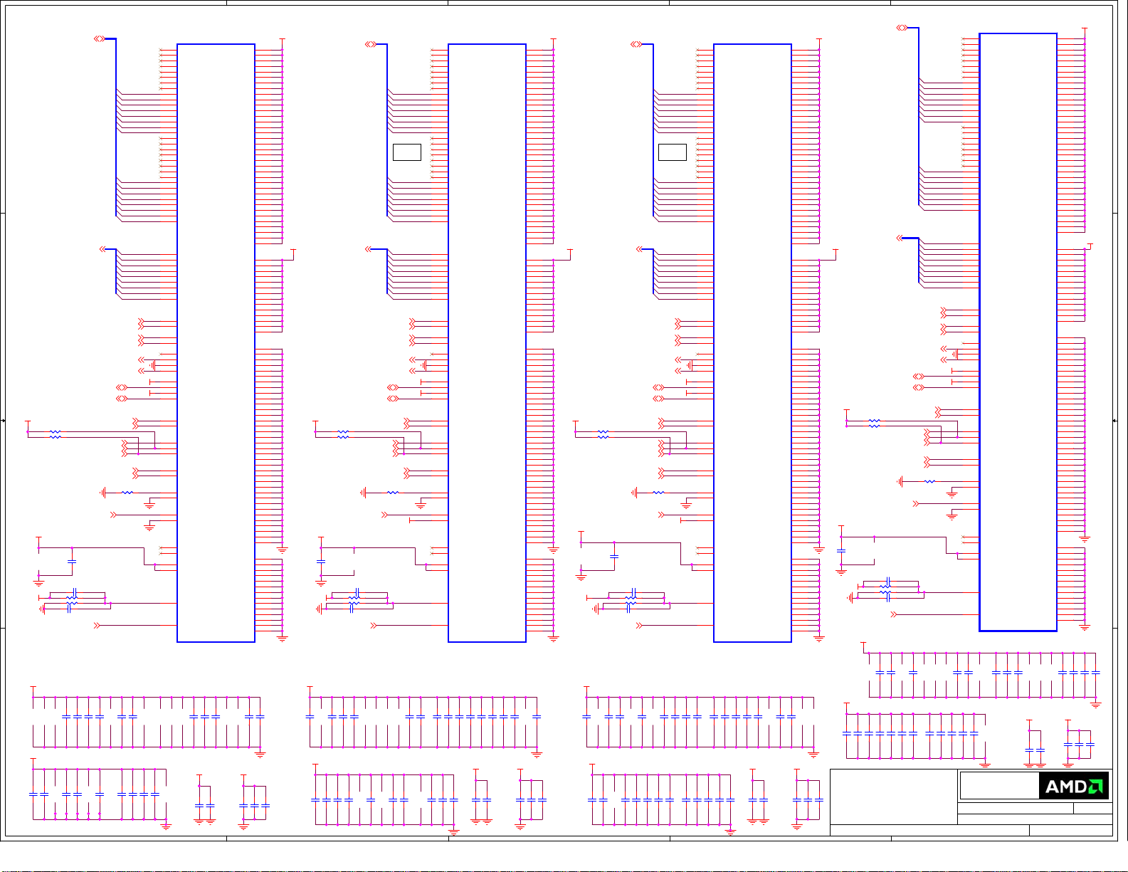
Page 5
5
(5) GDDR5 x16 MEM Channel B
DQB0_17
DQB0_16
DQB0_18
DQB0_19
DQB0_20
DDBIB0_2p.3
DDBIB0_1p.3
RASB0bp.3
CASB0bp.3
CSB0b_0p.3
WEB0bp.3
DRAM_RSTp.3,4
WCKB0_0p.3
WCKB0b_0p.3
WCKB0_1p.3
WCKB0b_1p.3
EDCB0_2p.3
EDCB0_1p.3
CKEB0p.3
CLKB0bp.3
CLKB0p.3
R2400 120RR2400 120R
1%
1%
DQB0_23
DQB0_21
DQB0_22
DQB0_10
DQB0_9
DQB0_11
DQB0_8
DQB0_14
DQB0_15
DQB0_13
DQB0_12
MAB0_8
MAB0_7
MAB0_6
MAB0_5
MAB0_4
MAB0_3
MAB0_2
MAB0_1
MAB0_0
+MVDD
+MVDD
VREFC_C0
D D
MAB0_[8..0]p.3
C C
+MVDD
R2403 120RR2403 120R
R2404 120RR2404 120R
+MEM_VREF
B B
C2400
C2400
100nF_6.3V
100nF_6.3V
C2401 1uF_6.3VC2401 1uF_6.3V
R2409 2.37KR2409 2.37K
+MVDD
R2410 5.49KR2410 5.49K
C2403 1uF_6.3VC2403 1uF_6.3V
ADBIB0p.3
1%
U2400
U2400
M2
DQ31 | DQ7
M4
DQ30 | DQ6
N2
DQ29 | DQ5
N4
DQ28 | DQ4
T2
DQ27 | DQ3
T4
DQ26 | DQ2
V2
DQ25 | DQ1
V4
DQ24 | DQ0
M13
DQ23 | DQ15
M11
DQ22 | DQ14
N13
DQ21 | DQ13
N11
DQ20 | DQ12
T13
DQ19 | DQ11
T11
DQ18 | DQ10
V13
DQ17 | DQ9
V11
DQ16 | DQ8
F13
DQ15 | DQ23
F11
DQ14 | DQ22
E13
DQ13 | DQ21
E11
DQ12 | DQ20
B13
DQ11 | DQ19
B11
DQ10 | DQ18
A13
DQ9 | DQ17
A11
DQ8 | DQ16
F2
DQ7 | DQ31
F4
DQ6 | DQ30
E2
DQ5 | DQ29
E4
DQ4 | DQ28
B2
DQ3 | DQ27
B4
DQ2 | DQ26
A2
DQ1 | DQ25
A4
DQ0 | DQ24
J5
RFU/A12/NC
K4
A7/A8 | A0/A10
K5
A6/A11 | A1/A9
K10
A5/BA1 | A3/BA3
K11
A4/BA2 | A2/BA0
H10
A3/BA3 | A5/BA1
H11
A2 /BA0 | A4/BA2
H5
A1/A9 | A6/A11
H4
A0/A10 | A7/A8
D4
WCK01 | WCK23
D5
WCK01# | WCK23#
P4
WCK23 | WCK01
P5
WCK23# | WCK01#
R2
EDC3 | EDC0
R13
EDC2 | EDC1
C13
EDC1 | EDC2
C2
EDC0 | EDC3
P2
DBI3# | DBI0#
P13
DBI2 #| DBI1#
D13
DBI1# | DBI2#
D2
DBI0# | DBI3#
G3
RAS# | CAS#
L3
CAS# | RAS#
J3
CKE#
J11
CK#
J12
CK
G12
CS# | WE#
L12
WE# | CS#
J13
ZQ
J10
SEN
J2
RESET#
J1
MF
A5
Vpp,NC
V5
Vpp,NC1
A10
VREFD1
V10
VREFD2
J14
VREFC
J4
ABI#
23F41GB7ME50
23F41GB7ME50
VDDQ-B1
VDDQ-B3
VDDQ-B12
VDDQ-B14
VDDQ-D1
VDDQ-D3
VDDQ-D12
VDDQ-D14
VDDQ-E5
VDDQ-E10
VDDQ-F1
VDDQ-F3
VDDQ-F12
VDDQ-F14
VDDQ-G2
VDDQ-G13
VDDQ-H3
VDDQ-H12
VDDQ-K3
VDDQ-K12
VDDQ-L2
VDDQ-L13
VDDQ-M1
VDDQ-M3
VDDQ-M12
VDDQ-M14
VDDQ-N5
VDDQ-N10
VDDQ-P1
VDDQ-P3
VDDQ-P12
VDDQ-P14
VDDQ-T1
VDDQ-T3
VDDQ-T12
VDDQ-T14
VDD-C10
VDD-D11
VDD-G11
VDD-G14
VDD-L11
VDD-L14
VDD-P11
VDD-R10
VSSQ-A1
VSSQ-A3
VSSQ-A12
VSSQ-A14
VSSQ-C1
VSSQ-C3
VSSQ-C4
VSSQ-C11
VSSQ-C12
VSSQ-C14
VSSQ-E1
VSSQ-E3
VSSQ-E12
VSSQ-E14
VSSQ-F5
VSSQ-F10
VSSQ-H2
VSSQ-H13
VSSQ-K2
VSSQ-K13
VSSQ-M5
VSSQ-M10
VSSQ-N1
VSSQ-N3
VSSQ-N12
VSSQ-N14
VSSQ-R1
VSSQ-R3
VSSQ-R4
VSSQ-R11
VSSQ-R12
VSSQ-R14
VSSQ-V1
VSSQ-V3
VSSQ-V12
VSSQ-V14
VSS-B10
VSS-D10
VSS-G10
VSS-H14
VSS-K14
VSS-L10
VSS-P10
VSS-T10
VDD-C5
VDD-G1
VDD-G4
VDD-L1
VDD-L4
VDD-R5
VSS-B5
VSS-G5
VSS-H1
VSS-K1
VSS-L5
VSS-T5
+MVDD
B1
B3
B12
B14
D1
D3
D12
D14
E5
E10
F1
F3
F12
F14
G2
G13
H3
H12
K3
K12
L2
L13
M1
M3
M12
M14
N5
N10
P1
P3
P12
P14
T1
T3
T12
T14
+MVDD
C5
C10
D11
G1
G4
G11
G14
L1
L4
L11
L14
P11
R5
R10
A1
A3
A12
A14
C1
C3
C4
C11
C12
C14
E1
E3
E12
E14
F5
F10
H2
H13
K2
K13
M5
M10
N1
N3
N12
N14
R1
R3
R4
R11
R12
R14
V1
V3
V12
V14
B5
B10
D10
G5
G10
H1
H14
K1
K14
L5
L10
P10
T5
T10
+MVDD
C2423 1uF_6.3VC2423 1uF_6.3V
C2410 2.2uF_4VC2410 2.2uF_4V
C2430 1uF_6.3VC2430 1uF_6.3V
C2405 2.2uF_4VC2405 2.2uF_4V
C2431 2.2uF_4VC2431 2.2uF_4V
C2414 1uF_6.3VC2414 1uF_6.3V
C2413 1uF_6.3VC2413 1uF_6.3V
C2443 1uF_6.3VC2443 1uF_6.3V
5
C2441 1uF_6.3VC2441 1uF_6.3V
C2432 1uF_6.3VC2432 1uF_6.3V
C2438 1uF_6.3VC2438 1uF_6.3V
C2417 2.2uF_4VC2417 2.2uF_4V
C2439 1uF_6.3VC2439 1uF_6.3V
C2407 2.2uF_4VC2407 2.2uF_4V
C2408 2.2uF_4VC2408 2.2uF_4V
C2406 2.2uF_4VC2406 2.2uF_4V
A A
C2435 2.2uF_4VC2435 2.2uF_4V
C2444 2.2uF_4VC2444 2.2uF_4V
C2434 2.2uF_4VC2434 2.2uF_4V
C2436 2.2uF_4VC2436 2.2uF_4V
C2418 2.2uF_4VC2418 2.2uF_4V
C2442 1uF_6.3VC2442 1uF_6.3V
C2419 2.2uF_4VC2419 2.2uF_4V
+MVDD
C2433 10uFC2433 10uF
C2421 1uF_6.3VC2421 1uF_6.3V
C2428 10uFC2428 10uF
C2422 2.2uF_4VC2422 2.2uF_4V
+MVDD
C2437 10uFC2437 10uF
C2440 10uFC2440 10uF
+MVDD+MVDD
C2429 10uFC2429 10uF
4
3
2
CH_B0 =U2400 & U2500 CH_B1 =U2600 & U2700
VDD-L1
VDD-L4
VSS-B5
VSS-G5
VSS-H1
VSS-K1
VSS-L5
VSS-T5
C2617 1uF_6.3VC2617 1uF_6.3V
C2635 10uFC2635 10uF
+MVDD
B1
B3
B12
B14
D1
D3
D12
D14
E5
E10
F1
F3
F12
F14
G2
G13
H3
H12
K3
K12
L2
L13
M1
M3
M12
M14
N5
N10
P1
P3
P12
P14
T1
T3
T12
T14
C5
C10
D11
G1
G4
G11
G14
L1
L4
L11
L14
P11
R5
R10
A1
A3
A12
A14
C1
C3
C4
C11
C12
C14
E1
E3
E12
E14
F5
F10
H2
H13
K2
K13
M5
M10
N1
N3
N12
N14
R1
R3
R4
R11
R12
R14
V1
V3
V12
V14
B5
B10
D10
G5
G10
H1
H14
K1
K14
L5
L10
P10
T5
T10
+MVDD
+MVDD
R2703 120RR2703 120R
R2704 120RR2704 120R
+MVDD
DQB1_[31..0]p.3
+MVDD
C2620 2.2uF_4VC2620 2.2uF_4V
C2618 2.2uF_4VC2618 2.2uF_4V
+MVDD
C2733 1uF_6.3VC2733 1uF_6.3V
C2734 2.2uF_4VC2734 2.2uF_4V
CONFIDENTIAL & PROPRIETARY TO ADVANCED MICRO DEVICES INC.
CONFIDENTIAL & PROPRIETARY TO ADVANCED MICRO DEVICES INC.
CONFIDENTIAL & PROPRIETARY TO ADVANCED MICRO DEVICES INC.
C2630 10uFC2630 10uF
C2634 10uFC2634 10uF
© 2007 Advanced Micro Devices
© 2007 Advanced Micro Devices
© 2007 Advanced Micro Devices
This AMD Board schematic and design is the exclusive property of AMD,
This AMD Board schematic and design is the exclusive property of AMD,
This AMD Board schematic and design is the exclusive property of AMD,
and is provided only to entities under a non-disclosure agreement
and is provided only to entities under a non-disclosure agreement
and is provided only to entities under a non-disclosure agreement
with AMD for evaluation purposes. Further distribution or disclosure
with AMD for evaluation purposes. Further distribution or disclosure
with AMD for evaluation purposes. Further distribution or disclosure
is strictly prohibited. Use of this schematic and design for any purpose
is strictly prohibited. Use of this schematic and design for any purpose
is strictly prohibited. Use of this schematic and design for any purpose
other than evaluation requires a Board Technology License Agreement
other than evaluation requires a Board Technology License Agreement
other than evaluation requires a Board Technology License Agreement
with AMD. AMD makes no representations or warranties of any kind
with AMD. AMD makes no representations or warranties of any kind
with AMD. AMD makes no representations or warranties of any kind
regarding this schematic and design, including, not limited to,
regarding this schematic and design, including, not limited to,
regarding this schematic and design, including, not limited to,
any implied warranty of merchantibility or fitness for a particular
any implied warranty of merchantibility or fitness for a particular
any implied warranty of merchantibility or fitness for a particular
purpose, and disclaims responsibility forany consequences resulting
purpose, and disclaims responsibility forany consequences resulting
purpose, and disclaims responsibility forany consequences resulting
from use of the information included herein.
from use of the information included herein.
from use of the information included herein.
Title
Title
Title
RH JUNIPER GDDR5 1GB DP+DP/HDMI+DVI /sVGA
RH JUNIPER GDDR5 1GB DP+DP/HDMI+DVI /sVGA
RH JUNIPER GDDR5 1GB DP+DP/HDMI+DVI /sVGA
MAB1_[8..0]p.3
C2702 1uF_6.3VC2702 1uF_6.3V
R2709 2.37KR2709 2.37K
R2710 5.49KR2710 5.49K
C2700 1uF_6.3VC2700 1uF_6.3V
C2742 2.2uF_4VC2742 2.2uF_4V
VDD-C5
VDD-G1
VDD-G4
VDD-L1
VDD-L4
VDD-R5
VSS-B5
VSS-G5
VSS-H1
VSS-K1
VSS-L5
VSS-T5
+MVDD
B1
B3
B12
B14
D1
D3
D12
D14
E5
E10
F1
F3
F12
F14
G2
G13
H3
H12
K3
K12
L2
L13
M1
M3
M12
M14
N5
N10
P1
P3
P12
P14
T1
T3
T12
T14
C5
C10
D11
G1
G4
G11
G14
L1
L4
L11
L14
P11
R5
R10
A1
A3
A12
A14
C1
C3
C4
C11
C12
C14
E1
E3
E12
E14
F5
F10
H2
H13
K2
K13
M5
M10
N1
N3
N12
N14
R1
R3
R4
R11
R12
R14
V1
V3
V12
V14
B5
B10
D10
G5
G10
H1
H14
K1
K14
L5
L10
P10
T5
T10
U2500
U2500
DQB0_[31..0]p.3
DQB0_2
DQB0_4
DQB0_1
DQB0_3
DQB0_0
DQB0_5
DQB0_7
DQB0_6
M=1
Mirror
DQB0_31
DQB0_29
DQB0_30
DQB0_28
DQB0_26
DQB0_25
DQB0_27
DQB0_24
MAB0_[8..0]p.3
R2503 120RR2503 120R
R2504 120RR2504 120R
DRAM_RSTp.3,4
+MEM_VREF
C2539 1uF_6.3VC2539 1uF_6.3V
R2509 2.37KR2509 2.37K
+MVDD +MVDD
R2510 5.49KR2510 5.49K
C2541 1uF_6.3VC2541 1uF_6.3V
DDBIB0_0p.3
DDBIB0_3p.3
CKEB0p.3
CLKB0bp.3
CLKB0p.3
WEB0bp.3
CSB0b_0p.3
R2501 120RR2501 120R
WCKB0_1p.3
WCKB0b_1p.3
WCKB0_0p.3
WCKB0b_0p.3
EDCB0_0p.3
EDCB0_3p.3
CASB0bp.3
RASB0bp.3
1%
1%
MAB0_8
MAB0_0
MAB0_1
MAB0_3
MAB0_2
MAB0_5
MAB0_4
MAB0_6
MAB0_7
+MVDD
+MVDD
+MVDD
C2544
C2544
100nF_6.3V
100nF_6.3V
1%
VREFC_C1
ADBIB0p.3
M2
DQ31 | DQ7
M4
DQ30 | DQ6
N2
DQ29 | DQ5
N4
DQ28 | DQ4
T2
DQ27 | DQ3
T4
DQ26 | DQ2
V2
DQ25 | DQ1
V4
DQ24 | DQ0
M13
DQ23 | DQ15
M11
DQ22 | DQ14
N13
DQ21 | DQ13
N11
DQ20 | DQ12
T13
DQ19 | DQ11
T11
DQ18 | DQ10
V13
DQ17 | DQ9
V11
DQ16 | DQ8
F13
DQ15 | DQ23
F11
DQ14 | DQ22
E13
DQ13 | DQ21
E11
DQ12 | DQ20
B13
DQ11 | DQ19
B11
DQ10 | DQ18
A13
DQ9 | DQ17
A11
DQ8 | DQ16
F2
DQ7 | DQ31
F4
DQ6 | DQ30
E2
DQ5 | DQ29
E4
DQ4 | DQ28
B2
DQ3 | DQ27
B4
DQ2 | DQ26
A2
DQ1 | DQ25
A4
DQ0 | DQ24
J5
RFU/A12/NC
K4
A7/A8 | A0/A10
K5
A6/A11 | A1/A9
K10
A5/BA1 | A3/BA3
K11
A4/BA2 | A2/BA0
H10
A3/BA3 | A5/BA1
H11
A2 /BA0 | A4/BA2
H5
A1/A9 | A6/A11
H4
A0/A10 | A7/A8
D4
WCK01 | WCK23
D5
WCK01# | WCK23#
P4
WCK23 | WCK01
P5
WCK23# | WCK01#
R2
EDC3 | EDC0
R13
EDC2 | EDC1
C13
EDC1 | EDC2
C2
EDC0 | EDC3
P2
DBI3# | DBI0#
P13
DBI2 #| DBI1#
D13
DBI1# | DBI2#
D2
DBI0# | DBI3#
G3
RAS# | CAS#
L3
CAS# | RAS#
J3
CKE#
J11
CK#
J12
CK
G12
CS# | WE#
L12
WE# | CS#
J13
ZQ
J10
SEN
J2
RESET#
J1
MF
A5
Vpp,NC
V5
Vpp,NC1
A10
VREFD1
V10
VREFD2
J14
VREFC
J4
ABI#
23F41GB7ME50
23F41GB7ME50
GDDR5
VDDQ-B1
VDDQ-B3
VDDQ-B12
VDDQ-B14
VDDQ-D1
VDDQ-D3
VDDQ-D12
VDDQ-D14
VDDQ-E5
VDDQ-E10
VDDQ-F1
VDDQ-F3
VDDQ-F12
VDDQ-F14
VDDQ-G2
VDDQ-G13
VDDQ-H3
VDDQ-H12
VDDQ-K3
VDDQ-K12
VDDQ-L2
VDDQ-L13
VDDQ-M1
VDDQ-M3
VDDQ-M12
VDDQ-M14
VDDQ-N5
VDDQ-N10
VDDQ-P1
VDDQ-P3
VDDQ-P12
VDDQ-P14
VDDQ-T1
VDDQ-T3
VDDQ-T12
VDDQ-T14
VDD-C10
VDD-D11
VDD-G11
VDD-G14
VDD-L11
VDD-L14
VDD-P11
VDD-R10
VSSQ-A1
VSSQ-A3
VSSQ-A12
VSSQ-A14
VSSQ-C1
VSSQ-C3
VSSQ-C4
VSSQ-C11
VSSQ-C12
VSSQ-C14
VSSQ-E1
VSSQ-E3
VSSQ-E12
VSSQ-E14
VSSQ-F5
VSSQ-F10
VSSQ-H2
VSSQ-H13
VSSQ-K2
VSSQ-K13
VSSQ-M5
VSSQ-M10
VSSQ-N1
VSSQ-N3
VSSQ-N12
VSSQ-N14
VSSQ-R1
VSSQ-R3
VSSQ-R4
VSSQ-R11
VSSQ-R12
VSSQ-R14
VSSQ-V1
VSSQ-V3
VSSQ-V12
VSSQ-V14
VSS-B10
VSS-D10
VSS-G10
VSS-H14
VSS-K14
VSS-L10
VSS-P10
VSS-T10
+MVDD
C2503 1uF_6.3VC2503 1uF_6.3V
C2504 2.2uF_4VC2504 2.2uF_4V
C2506 1uF_6.3VC2506 1uF_6.3V
C2508 1uF_6.3VC2508 1uF_6.3V
C2509 1uF_6.3VC2509 1uF_6.3V
C2510 1uF_6.3VC2510 1uF_6.3V
C2511 2.2uF_4VC2511 2.2uF_4V
C2512 2.2uF_4VC2512 2.2uF_4V
C2515 1uF_6.3VC2515 1uF_6.3V
C2514 1uF_6.3VC2514 1uF_6.3V
C2516 1uF_6.3VC2516 1uF_6.3V
C2519 1uF_6.3VC2519 1uF_6.3V
C2520 1uF_6.3VC2520 1uF_6.3V
+MVDD
C2538 2.2uF_4VC2538 2.2uF_4V
C2536 1uF_6.3VC2536 1uF_6.3V
C2537 2.2uF_4VC2537 2.2uF_4V
C2525 1uF_6.3VC2525 1uF_6.3V
C2526 1uF_6.3VC2526 1uF_6.3V
4
C2521 2.2uF_4VC2521 2.2uF_4V
C2532 1uF_6.3VC2532 1uF_6.3V
C2527 2.2uF_4VC2527 2.2uF_4V
C2522 1uF_6.3VC2522 1uF_6.3V
C2529 1uF_6.3VC2529 1uF_6.3V
C2523 1uF_6.3VC2523 1uF_6.3V
+MVDD
C2535 10uFC2535 10uFC2513 1uF_6.3VC2513 1uF_6.3V
+MVDD
C2524 10uFC2524 10uF
C2533 10uFC2533 10uF
C2530 10uFC2530 10uF
C2638 1uF_6.3VC2638 1uF_6.3V
C2534 10uFC2534 10uF
3
U2600
U2600
DQB1_[31..0]p.3DQB0_[31..0]p.3
DQB1_15
DQB1_14
DQB1_13
DQB1_8
DQB1_12
DQB1_10
DQB1_11
DQB1_9
M=1
Mirror
DQB1_22
DQB1_21
DQB1_20
DQB1_23
DQB1_19
DQB1_16
DQB1_18
DQB1_17
+MVDD
+MVDD+MVDD
R2603 120RR2603 120R
R2604 120RR2604 120R
MAB1_[8..0]p.3
DRAM_RSTp.3,4
DDBIB1_1p.3
DDBIB1_2p.3
CASB1bp.3
RASB1bp.3
WEB1bp.3
CSB1b_0p.3
WCKB1_1p.3
WCKB1b_1p.3
WCKB1_0p.3
WCKB1b_0p.3
EDCB1_1p.3
EDCB1_2p.3
CKEB1p.3
CLKB1bp.3
CLKB1p.3
R2601 120RR2601 120R
+MVDD
MAB1_8
MAB1_0
MAB1_1
MAB1_3
MAB1_2
MAB1_5
MAB1_4
MAB1_6
MAB1_7
+MVDD
+MVDD
1%
+MEM_VREF +MEM_VREF
C2640
C2640
100nF_6.3V
100nF_6.3V
C2639 1uF_6.3VC2639 1uF_6.3V
R2609 2.37KR2609 2.37K
1%
R2610 5.49KR2610 5.49K
C2641 1uF_6.3VC2641 1uF_6.3V
VREFC_D0
1%
ADBIB1p.3
M2
DQ31 | DQ7
M4
DQ30 | DQ6
N2
DQ29 | DQ5
N4
DQ28 | DQ4
T2
DQ27 | DQ3
T4
DQ26 | DQ2
V2
DQ25 | DQ1
V4
DQ24 | DQ0
M13
DQ23 | DQ15
M11
DQ22 | DQ14
N13
DQ21 | DQ13
N11
DQ20 | DQ12
T13
DQ19 | DQ11
T11
DQ18 | DQ10
V13
DQ17 | DQ9
V11
DQ16 | DQ8
F13
DQ15 | DQ23
F11
DQ14 | DQ22
E13
DQ13 | DQ21
E11
DQ12 | DQ20
B13
DQ11 | DQ19
B11
DQ10 | DQ18
A13
DQ9 | DQ17
A11
DQ8 | DQ16
F2
DQ7 | DQ31
F4
DQ6 | DQ30
E2
DQ5 | DQ29
E4
DQ4 | DQ28
B2
DQ3 | DQ27
B4
DQ2 | DQ26
A2
DQ1 | DQ25
A4
DQ0 | DQ24
J5
RFU/A12/NC
K4
A7/A8 | A0/A10
K5
A6/A11 | A1/A9
K10
A5/BA1 | A3/BA3
K11
A4/BA2 | A2/BA0
H10
A3/BA3 | A5/BA1
H11
A2 /BA0 | A4/BA2
H5
A1/A9 | A6/A11
H4
A0/A10 | A7/A8
D4
WCK01 | WCK23
D5
WCK01# | WCK23#
P4
WCK23 | WCK01
P5
WCK23# | WCK01#
R2
EDC3 | EDC0
R13
EDC2 | EDC1
C13
EDC1 | EDC2
C2
EDC0 | EDC3
P2
DBI3# | DBI0#
P13
DBI2 #| DBI1#
D13
DBI1# | DBI2#
D2
DBI0# | DBI3#
G3
RAS# | CAS#
L3
CAS# | RAS#
J3
CKE#
J11
CK#
J12
CK
G12
CS# | WE#
L12
WE# | CS#
J13
ZQ
J10
SEN
J2
RESET#
J1
MF
A5
Vpp,NC
V5
Vpp,NC1
A10
VREFD1
V10
VREFD2
J14
VREFC
J4
ABI#
23F41GB7ME50
23F41GB7ME50
GDDR5
VDDQ-B1
VDDQ-B3
VDDQ-B12
VDDQ-B14
VDDQ-D1
VDDQ-D3
VDDQ-D12
VDDQ-D14
VDDQ-E5
VDDQ-E10
VDDQ-F1
VDDQ-F3
VDDQ-F12
VDDQ-F14
VDDQ-G2
VDDQ-G13
VDDQ-H3
VDDQ-H12
VDDQ-K3
VDDQ-K12
VDDQ-L2
VDDQ-L13
VDDQ-M1
VDDQ-M3
VDDQ-M12
VDDQ-M14
VDDQ-N5
VDDQ-N10
VDDQ-P1
VDDQ-P3
VDDQ-P12
VDDQ-P14
VDDQ-T1
VDDQ-T3
VDDQ-T12
VDDQ-T14
VDD-C5
VDD-C10
VDD-D11
VDD-G1
VDD-G4
VDD-G11
VDD-G14
VDD-L11
VDD-L14
VDD-P11
VDD-R5
VDD-R10
VSSQ-A1
VSSQ-A3
VSSQ-A12
VSSQ-A14
VSSQ-C1
VSSQ-C3
VSSQ-C4
VSSQ-C11
VSSQ-C12
VSSQ-C14
VSSQ-E1
VSSQ-E3
VSSQ-E12
VSSQ-E14
VSSQ-F5
VSSQ-F10
VSSQ-H2
VSSQ-H13
VSSQ-K2
VSSQ-K13
VSSQ-M5
VSSQ-M10
VSSQ-N1
VSSQ-N3
VSSQ-N12
VSSQ-N14
VSSQ-R1
VSSQ-R3
VSSQ-R4
VSSQ-R11
VSSQ-R12
VSSQ-R14
VSSQ-V1
VSSQ-V3
VSSQ-V12
VSSQ-V14
VSS-B10
VSS-D10
VSS-G10
VSS-H14
VSS-K14
VSS-L10
VSS-P10
VSS-T10
+MVDD
C2643 1uF_6.3VC2643 1uF_6.3V
C2631 2.2uF_4VC2631 2.2uF_4V
C2600 1uF_6.3VC2600 1uF_6.3V
C2621 1uF_6.3VC2621 1uF_6.3V
C2622 2.2uF_4VC2622 2.2uF_4V
C2623 2.2uF_4VC2623 2.2uF_4V
C2604 1uF_6.3VC2604 1uF_6.3V
C2628 2.2uF_4VC2628 2.2uF_4V
C2632 2.2uF_4VC2632 2.2uF_4V
C2607 1uF_6.3VC2607 1uF_6.3V
C2606 1uF_6.3VC2606 1uF_6.3V
C2626 1uF_6.3VC2626 1uF_6.3V
C2608 1uF_6.3VC2608 1uF_6.3V
C2627 1uF_6.3VC2627 1uF_6.3V
C2609 1uF_6.3VC2609 1uF_6.3V
C2637 1uF_6.3VC2637 1uF_6.3V
C2636 1uF_6.3VC2636 1uF_6.3V
C2629 1uF_6.3VC2629 1uF_6.3V
C2612 2.2uF_4VC2612 2.2uF_4V
+MVDD
C2613 2.2uF_4VC2613 2.2uF_4V
C2625 10uFC2625 10uF
C2614 2.2uF_4VC2614 2.2uF_4V
C2633 10uFC2633 10uF
C2615 1uF_6.3VC2615 1uF_6.3V
+MVDD
2
ADBIB1p.3
C2743 2.2uF_4VC2743 2.2uF_4V
DDBIB1_3p.3
DDBIB1_0p.3
DRAM_RSTp.3,4
C2701
C2701
100nF_6.3V
100nF_6.3V
C2707 2.2uF_4VC2707 2.2uF_4V
C2726 2.2uF_4VC2726 2.2uF_4V
WCKB1_0p.3
WCKB1b_0p.3
WCKB1_1p.3
WCKB1b_1p.3
EDCB1_3p.3
EDCB1_0p.3
RASB1bp.3
CASB1bp.3
CKEB1p.3
CLKB1bp.3
CLKB1p.3
CSB1b_0p.3
WEB1bp.3
R2700 120RR2700 120R
1%
1%
C2732 2.2uF_4VC2732 2.2uF_4V
C2727 2.2uF_4VC2727 2.2uF_4V
DQB1_26
DQB1_25
DQB1_27
DQB1_24
DQB1_30
DQB1_28
DQB1_29
DQB1_31
DQB1_1
DQB1_0
DQB1_2
DQB1_3
DQB1_5
DQB1_6
DQB1_4
DQB1_7
MAB1_8
MAB1_7
MAB1_6
MAB1_5
MAB1_4
MAB1_3
MAB1_2
MAB1_1
MAB1_0
+MVDD
+MVDD
VREFC_D1
C2730 2.2uF_4VC2730 2.2uF_4V
1%
C2712 1uF_6.3VC2712 1uF_6.3V
C2731 1uF_6.3VC2731 1uF_6.3V
1
U2700
U2700
M2
DQ31 | DQ7
M4
DQ30 | DQ6
N2
DQ29 | DQ5
N4
DQ28 | DQ4
T2
DQ27 | DQ3
T4
DQ26 | DQ2
V2
DQ25 | DQ1
V4
DQ24 | DQ0
M13
DQ23 | DQ15
M11
DQ22 | DQ14
N13
DQ21 | DQ13
N11
DQ20 | DQ12
T13
DQ19 | DQ11
T11
DQ18 | DQ10
V13
DQ17 | DQ9
V11
DQ16 | DQ8
F13
DQ15 | DQ23
F11
DQ14 | DQ22
E13
DQ13 | DQ21
E11
DQ12 | DQ20
B13
DQ11 | DQ19
B11
DQ10 | DQ18
A13
DQ9 | DQ17
A11
DQ8 | DQ16
F2
DQ7 | DQ31
F4
DQ6 | DQ30
E2
DQ5 | DQ29
E4
DQ4 | DQ28
B2
DQ3 | DQ27
B4
DQ2 | DQ26
A2
DQ1 | DQ25
A4
DQ0 | DQ24
J5
RFU/A12/NC
K4
A7/A8 | A0/A10
K5
A6/A11 | A1/A9
K10
A5/BA1 | A3/BA3
K11
A4/BA2 | A2/BA0
H10
A3/BA3 | A5/BA1
H11
A2 /BA0 | A4/BA2
H5
A1/A9 | A6/A11
H4
A0/A10 | A7/A8
D4
WCK01 | WCK23
D5
WCK01# | WCK23#
P4
WCK23 | WCK01
P5
WCK23# | WCK01#
R2
EDC3 | EDC0
R13
EDC2 | EDC1
C13
EDC1 | EDC2
C2
EDC0 | EDC3
P2
DBI3# | DBI0#
P13
DBI2 #| DBI1#
D13
DBI1# | DBI2#
D2
DBI0# | DBI3#
G3
RAS# | CAS#
L3
CAS# | RAS#
J3
CKE#
J11
CK#
J12
CK
G12
CS# | WE#
L12
WE# | CS#
J13
ZQ
J10
SEN
J2
RESET#
J1
MF
A5
Vpp,NC
V5
Vpp,NC1
A10
VREFD1
V10
VREFD2
J14
VREFC
J4
ABI#
23F41GB7ME50
23F41GB7ME50
C2713 2.2uF_4VC2713 2.2uF_4V
C2715 1uF_6.3VC2715 1uF_6.3V
C2729 1uF_6.3VC2729 1uF_6.3V
C2741 1uF_6.3VC2741 1uF_6.3V
C2728 1uF_6.3VC2728 1uF_6.3V
C2735 1uF_6.3VC2735 1uF_6.3V
Advanced Micro Devices Inc.
Advanced Micro Devices Inc.
Advanced Micro Devices Inc.
1 Commerce Valley Drive East
1 Commerce Valley Drive East
1 Commerce Valley Drive East
Markham, Ontario
Markham, Ontario
Markham, Ontario
Tuesday, November 10, 2009
Tuesday, November 10, 2009
Tuesday, November 10, 2009
Sheet
Sheet
Sheet
of
521
of
521
of
521
1
TOPBOTTOM
GDDR5
C2717 2.2uF_4VC2717 2.2uF_4V
+MVDD
C2736 10uFC2736 10uF
C2718 1uF_6.3VC2718 1uF_6.3V
C2737 10uFC2737 10uF
Doc No.
Doc No.
Doc No.
VDDQ-B1
VDDQ-B3
VDDQ-B12
VDDQ-B14
VDDQ-D1
VDDQ-D3
VDDQ-D12
VDDQ-D14
VDDQ-E5
VDDQ-E10
VDDQ-F1
VDDQ-F3
VDDQ-F12
VDDQ-F14
VDDQ-G2
VDDQ-G13
VDDQ-H3
VDDQ-H12
VDDQ-K3
VDDQ-K12
VDDQ-L2
VDDQ-L13
VDDQ-M1
VDDQ-M3
VDDQ-M12
VDDQ-M14
VDDQ-N5
VDDQ-N10
VDDQ-P1
VDDQ-P3
VDDQ-P12
VDDQ-P14
VDDQ-T1
VDDQ-T3
VDDQ-T12
VDDQ-T14
VDD-C10
VDD-D11
VDD-G11
VDD-G14
VDD-P11
VDD-R10
VSSQ-A1
VSSQ-A3
VSSQ-A12
VSSQ-A14
VSSQ-C1
VSSQ-C3
VSSQ-C4
VSSQ-C11
VSSQ-C12
VSSQ-C14
VSSQ-E1
VSSQ-E3
VSSQ-E12
VSSQ-E14
VSSQ-F5
VSSQ-F10
VSSQ-H2
VSSQ-H13
VSSQ-K2
VSSQ-K13
VSSQ-M5
VSSQ-M10
VSSQ-N1
VSSQ-N3
VSSQ-N12
VSSQ-N14
VSSQ-R1
VSSQ-R3
VSSQ-R4
VSSQ-R11
VSSQ-R12
VSSQ-R14
VSSQ-V1
VSSQ-V3
VSSQ-V12
VSSQ-V14
VSS-G10
C2719 1uF_6.3VC2719 1uF_6.3V
VDD-C5
VDD-G1
VDD-G4
VDD-L1
VDD-L4
VDD-L11
VDD-L14
VDD-R5
VSS-B5
VSS-B10
VSS-D10
VSS-G5
VSS-H1
VSS-H14
VSS-K1
VSS-K14
VSS-L5
VSS-L10
VSS-P10
VSS-T5
VSS-T10
C2721 2.2uF_4VC2721 2.2uF_4V
+MVDD
C2738 10uFC2738 10uF
102-C01301-00
102-C01301-00
102-C01301-00
B1
B3
B12
B14
D1
D3
D12
D14
E5
E10
F1
F3
F12
F14
G2
G13
H3
H12
K3
K12
L2
L13
M1
M3
M12
M14
N5
N10
P1
P3
P12
P14
T1
T3
T12
T14
C5
C10
D11
G1
G4
G11
G14
L1
L4
L11
L14
P11
R5
R10
A1
A3
A12
A14
C1
C3
C4
C11
C12
C14
E1
E3
E12
E14
F5
F10
H2
H13
K2
K13
M5
M10
N1
N3
N12
N14
R1
R3
R4
R11
R12
R14
V1
V3
V12
V14
B5
B10
D10
G5
G10
H1
H14
K1
K14
L5
L10
P10
T5
T10
C2722 1uF_6.3VC2722 1uF_6.3V
C2739 10uFC2739 10uF
RevDate:
RevDate:
RevDate:
+MVDD
+MVDD
C2723 2.2uF_4VC2723 2.2uF_4V
C2740 10uFC2740 10uF
50
50
50
C2724 1uF_6.3VC2724 1uF_6.3V
Page 6
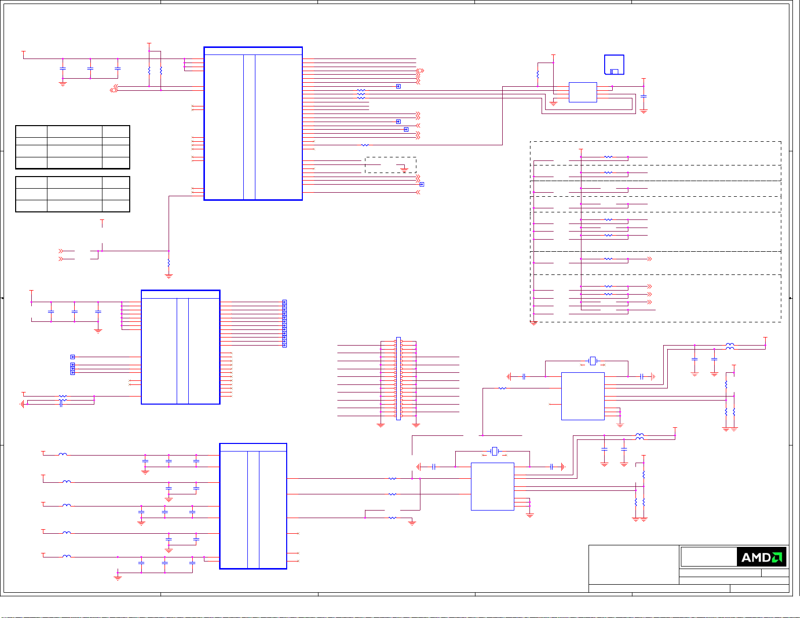
5
4
(06) JUNIPER GPIOs Strap CF XTAL OSC
3
2
1
+3.3V_BUS
C2
C1
100nF_6.3VC2100nF_6.3V
Function Device
MVDDQ, MVDDC, VDDCI
VREF CONTROL
Function Device
Temperature Sensor
C5
1uF_6.3VC51uF_6.3V
TP84 35milTP84 35mil
TP85 35milTP85 35mil
TP86 35milTP86 35mil
TP87 35milTP87 35mil
R17 221RR17 221R
R18 110RR18 110R
C8 100nF_6.3VC8 100nF_6.3V
+1.8V
B1 BLM15AG121SN1DB1 BLM15AG121SN1D
+1V
B4 BLM15AG121SN1DB4 BLM15AG121SN1D
+1.8V
B5 BLM15AG121SN1DB5 BLM15AG121SN1D
+1V
B6 BLM15AG121SN1DB6 BLM15AG121SN1D
+1.8V
B7 BLM15AG121SN1DB7 BLM15AG121SN1D
100nF_6.3VC1100nF_6.3V
DNI
DNI
C6
1uF_6.3VC61uF_6.3V
5
SCLp.17
SDAp.17
+1.8V
C7
1uF_6.3VC71uF_6.3V
DVOCLK
DVPCNTL_0
DVPCNTL_1
DVPCNTL_2
VREFG
UP6266
LM96163
D D
SCL / SDA BUS:
I2C Address
0x80 VDDC CONTROLLER
Write
Read0x81
0xA0, 0xA2
0xA4
DDC6 BUS:
I2C Address
0x98 LM96163 - External
NOTE: If connecting
C C
1V_LDO_POK, only one
pull up either to 1.8V or
3.3V
1.8V_LDO_POKp.15
1V_LDO_POKp.1,15,18
+1.8V
DNI
B B
+1.8V
A A
+3.3V_BUS
R22
C3
100nF_6.3VC3100nF_6.3V
ST
UPIVDDC CONTROLLER0x70
10uF
10uF
10uF
10uF
R22
R27
R27
2.2K
2.2K
2.2K
2.2K
SCL
SDA
PWRGOOD:
InternalSingal.
Bringto0RPDfor
verification.
PWRGOOD
U1F
U1F
AD12
AF11
AF12
AF13
AF15
AG11
AG13
AG15
AR1
AP8
AW8
AR3
AR8
AU8
AH13
JUNIPER XT A12 HF MVD SLT BIN1 TSMC FB12
JUNIPER XT A12 HF MVD SLT BIN1 TSMC FB12
C13
C13
10uF
10uF
C18
C18
C25
C25
VDDR4#1
VDDR4#2
VDDR4#3
VDDR4#4
VDDR4#5
VDDR4#6
VDDR4#7
VDDR4#8
DVPCLK
DVPCNTL_0
DVPCNTL_1
DVPCNTL_2
DVPCNTL_MVP_0
DVPCNTL_MVP_1
VREFG
C14
C14
1uF_6.3V
1uF_6.3V
C16
C16
1uF_6.3V
1uF_6.3V
C19
C19
1uF_6.3V
1uF_6.3V
C21
C21
1uF_6.3V
1uF_6.3V
C26
C26
1uF_6.3V
1uF_6.3V
PART 6 OF 15
PART 6 OF 15
+DPLL_PVDD
100nF_6.3V
100nF_6.3V
+DPLL_VDDC
100nF_6.3V
100nF_6.3V
100nF_6.3V
100nF_6.3V
100nF_6.3V
100nF_6.3V
C27
C27
100nF_6.3V
100nF_6.3V
U1E
U1E
AF23
VDDR3#1
AF24
VDDR3#2
AG23
VDDR3#3
AG24
VDDR3#4
AK26
SCL
AJ26
SDA
AJ30
DDC6CLK
AJ31
DDC6DATA
AF35
RSVD#1
AG36
RSVD#2
AJ27
RSVD#3
AK27
RSVD#4
AN36
RSVD#6
AP37
RSVD#7
AJ21
NC#1
AK21
NC#2
AH16
PWRGOOD
JUNIPER XT A12 HF MVD SLT BIN1 TSMC FB12
JUNIPER XT A12 HF MVD SLT BIN1 TSMC FB12
R331KR33
1K
DVPDATA_0
DVPDATA_1
DVPDATA_2
DVPDATA_3
DVPDATA_4
DVPDATA_5
DVPDATA_6
DVPDATA_7
DVPDATA_8
DVPDATA_9
DVPDATA_10
DVPDATA_11
D
D
DVPDATA_12
V
V
DVPDATA_13
P
P
DVPDATA_14
DVPDATA_15
DVPDATA_16
DVPDATA_17
DVPDATA_18
DVPDATA_19
DVPDATA_20
DVPDATA_21
DVPDATA_22
DVPDATA_23
AM32
C15
C15
AN32
AN31
C17
C17
C20
C20
+SPV10
C22
C22
AM10
AN10
AN9
H7
H8
+SPV18
+MPV18
PART 5 OF 15
PART 5 OF 15
G
G
P
P
I
I
O
O
GPIO_0
GPIO_1
GPIO_2
GPIO_3_SMBDATA
GPIO_4_SMBCLK
GPIO_5_AC_BATT
GPIO_6_TACH
GPIO_7_BLON
GPIO_8_ROMSO
GPIO_9_ROMSI
GPIO_10_ROMSCK
GPIO_11
GPIO_12
GPIO_13
GPIO_14_HPD2
GPIO_15_PWRCNTL_0
GPIO_16_SSIN
GPIO_17_THERMAL_INT
GPIO_18_HPD3
GPIO_19_CTF
GPIO_20_PWRCNTL_1
GPIO_21_BB_EN
GPIO_22_ROMCSB
GPIO_23_CLKREQB
GENERICA
GENERICB
GENERICC
GENERICD
GENERICE_HPD4
GENERICF_HPD5
GENERICG_HPD6
HPD1
CrossFire Card-Edge
AU1
DVPDATA_0
AU3
DVPDATA_1
AW3
DVPDATA_2
AP6
DVPDATA_3
AW5
DVPDATA_4
AU5
DVPDATA_5
AR6
DVPDATA_6
AW6
DVPDATA_7
AU6
DVPDATA_8
AT7
DVPDATA_9
AV7
DVPDATA_10
AN7
DVPDATA_11
AV9
AT9
AR10
AW10
AU10
AP10
AV11
AT11
AR12
AW12
AU12
AP12
U1G
U1G
PART 7 OF 15
PART 7 OF 15
DPLL_PVDD
DPLL_PVSS
P
P
DPLL_VDDC
L
L
L
L
S
S
X
X
SPV18
T
T
A
A
SPVSS
L
L
SPV10
MPV18#1
MPV18#2
JUNIPER XT A12 HF MVD SLT BIN1 TSMC FB12
JUNIPER XT A12 HF MVD SLT BIN1 TSMC FB12
4
XO_IN2
XO_IN
XTALIN
XTALOUT
CLKTESTA
CLKTESTB
TP6035mil TP6035mil
TP6135mil TP6135mil
TP6235mil TP6235mil
TP6335mil TP6335mil
TP6435mil TP6435mil
TP6535mil TP6535mil
TP6635mil TP6635mil
TP6735mil TP6735mil
TP6835mil TP6835mil
TP6935mil TP6935mil
TP7035mil TP7035mil
TP7135mil TP7135mil
FOR740:DNIR28/TR19‐
XO_IN/2AREGNDon740/730
AW35
AW34
AV33
XTALIN
AU34
AK10
AL10
route50ohmssingle‐ended/100ohmsdiffandkeepshort
AH20
GPIO_0
AH18
GPIO_1
AN16
GPIO_2
AH23
GPIO_3_SMBDATA
AJ23
GPIO_4_SMBCLK
AH17
GPIO_5
AJ17
GPIO_6_TACH
AK17
GPIO_7
AJ13
GPIO_8
AH15
GPIO_9
AJ16
GPIO_10
AK16
GPIO_11
AL16
GPIO_12
AM16
GPIO_13
AM14
GPIO_14_HPD2
AM13
GPIO_15_PWRCNTL_0
AK14
GPIO_16
AG30
GPIO_17_ThermINT
AN14
AM17
GPIO_19_CTF
AL13
GPIO_20_PWRCNTL_1
AJ14
AK13
GPIO_22_ROMCSb
AN13
AJ19
GENERICA
AK19
GENERICB
AJ20
AK20
GENERICD
AJ24
GENERICE_HPD4
AH26
GENERICF_HPD5
AH24
N29218647
AK24
Upper Cable Card Edge
DVOCLK
DVPCNTL_2
DVPDATA_1
DVPDATA_3
DVPDATA_5
DVPDATA_7
DVPDATA_9
DVPDATA_11
DVPCNTL_1
GENERICD
XO_IN2
XO_IN CLK_27M
GPIO_0
GPIO_1
63
RP1C33R RP1C33R
81
RP1A33R RP1A33R
72
RP1B33R RP1B33R
54
RP1D33R RP1D33R
CONNECTATASIC
GPIO_2
DNI
GPIO_3_SMBDATA p.1
GPIO_4_SMBCLK p.1
GPIO_5 p.17
GPIO_6_TACH p.18
TP9235mil TP9235mil
GPIO_14_HPD2 p.9
GPIO_15_PWRCNTL_0 p.17
TP93TP93
GPIO_17_ThermINT p.17,18,19
TP98TP98
GPIO_19_CTF p.18
GPIO_20_PWRCNTL_1 p.17
GPIO_22_ROMCSb_R
CLKREQ#requiresopendrainconnection,
andcannotbeusedaspinstrap
GENERICE_HPD4 p.9
GENERICF_HPD5 p.9
TP97TP97
HPD1 p.8
or Bundle B
Lower Cable Card Edge
or Bundle A (closer to the bracket)
Dividerfor1.8V
signaling.
DNI
DNI
1
3
5
7
9
11
13
15
17
19
21
23
25
27
29 30
31
33
35
37
39
R28 10RR28 10R
TR19 0RTR19 0R
R23 221RR23 221R
3
2
J2J2
4
6
8
10
12
14
16
18
20
22
24
26
28
32
34
36
38
40
DVPDATA_0
DVPDATA_2
DVPDATA_4
DVPDATA_6
DVPDATA_8
DVPDATA_10
DVPCNTL_0
GPIO_2
GENERICA_100M
C11 20pF_50VC11 20pF_50V
CLK_100M
C36 20pF_50VC36 20pF_50V
MR34 10RMR34 10R
OVERLAPR34/MR34
GENERICA
Y1
Y1
27.000MHz_10PPM_30R
27.000MHz_10PPM_30R
2 4
VDD_100M
SS_SEL0
SS_SEL1
GND_100M
GND_27M
GND_PAD
XTALIN
31
1
4
8
7
3
6
2
11
XOUT_OSC XIN_OSC
U12
U12
10
XTALOUT
100M_OUT5VDD_27M
9
27M_OUT
SL16010DCT
SL16010DCT
+3.3V_BUS
R14
R14
2.2K
2.2K
U11
U11
1
CE#
GPIO_8_R
2
SO
3
WP#
GND4SI
PM25LV010A-100SCE
PM25LV010A-100SCE
1MbitROM
+3.3V_BUS
DNI
DNI
DNI
DNI
DNI
DNI
DNI
DNI
DNI
DNI
DNI
DNI
27.000MHz_10PPM_30R
27.000MHz_10PPM_30R
XOUT_OSC_GENA XIN_OSC_GENA
U2
U2
10
C12
C12
XTALOUT
100M_OUT5VDD_27M
9
27M_OUT
SL16010DCT
SL16010DCT
2
CLK_100M_GENA
20pF_50V
20pF_50V
VDD33_100M
VDD33_27M
BIOS1
BIOS1
VIDEO BIOS
FIRMWARE
BIOS
BIOS
HOLD#
VCC
SCK
113-C013XX-XXX
113-C013XX-XXX
8
7
6
5
GPIO_10_R
GPIO_9_R
+3.3V_BUS
C4
100nF_6.3VC4100nF_6.3V
PIN BASED STRAPS
31
1
4
8
7
3
6
2
11
C10
C10
100nF_6.3V
100nF_6.3V
GPIO_0
GPIO_1
GPIO_2
GPIO_9_R
GPIO_13
GPIO_12GPIO_12
GPIO_11
V1SYNC
H1SYNC
H2SYNC
GPIO_8_R
C37
C37
20pF_50V
20pF_50V
VDD33_100M_GENA
VDD33_27M_GENA
B2 BLM15AG121SN1DB2 BLM15AG121SN1D
B3 BLM15AG121SN1DB3 BLM15AG121SN1D
+3.3V_BUS
R21 5.1KR21 5.1K
MR15 5.1KMR15 5.1K
MR16 5.1KMR16 5.1K
V2SYNC p.7
V1SYNC p.7
H1SYNC p.7
H2SYNC p.7
100nF_6.3V
100nF_6.3V
SS_SEL0_GENA
SS_SEL1_GENA
+3.3V_BUS
R1 10KR1 10K
R2 10KR2 10K
DNI
DNI
R6 10KR6 10K
DNI
R8 10KR8 10K
DNI
R9 10KR9 10K
R10 10KR10 10K
DNI
R11 10KR11 10K
DNI
DNI
Y2
Y2
2 4
XTALIN
VDD_100M
SS_SEL0
SS_SEL1
GND_100M
GND_27M
GND_PAD
C9
100nF_6.3VC9100nF_6.3V
SS_SEL0
SS_SEL1
CONFIDENTIAL & PROPRIETARY TO ADVANCED MICRO DEVICES INC.
CONFIDENTIAL & PROPRIETARY TO ADVANCED MICRO DEVICES INC.
CONFIDENTIAL & PROPRIETARY TO ADVANCED MICRO DEVICES INC.
© 2007 Advanced Micro Devices
© 2007 Advanced Micro Devices
© 2007 Advanced Micro Devices
This AMD Board schematic and design is the exclusive property of AMD,
This AMD Board schematic and design is the exclusive property of AMD,
This AMD Board schematic and design is the exclusive property of AMD,
and is provided only to entities under a non-disclosure agreement
and is provided only to entities under a non-disclosure agreement
and is provided only to entities under a non-disclosure agreement
with AMD for evaluation purposes. Further distribution or disclosure
with AMD for evaluation purposes. Further distribution or disclosure
with AMD for evaluation purposes. Further distribution or disclosure
is strictly prohibited. Use of this schematic and design for any purpose
is strictly prohibited. Use of this schematic and design for any purpose
is strictly prohibited. Use of this schematic and design for any purpose
other than evaluation requires a Board Technology License Agreement
other than evaluation requires a Board Technology License Agreement
other than evaluation requires a Board Technology License Agreement
with AMD. AMD makes no representations or warranties of any kind
with AMD. AMD makes no representations or warranties of any kind
with AMD. AMD makes no representations or warranties of any kind
regarding this schematic and design, including, not limited to,
regarding this schematic and design, including, not limited to,
regarding this schematic and design, including, not limited to,
any implied warranty of merchantibility or fitness for a particular
any implied warranty of merchantibility or fitness for a particular
any implied warranty of merchantibility or fitness for a particular
purpose, and disclaims responsibility forany consequences resulting
purpose, and disclaims responsibility forany consequences resulting
purpose, and disclaims responsibility forany consequences resulting
from use of the information included herein.
from use of the information included herein.
from use of the information included herein.
Title
Title
Title
RH JUNIPER GDDR5 1GB DP+DP/HDMI+DVI /sVGA
RH JUNIPER GDDR5 1GB DP+DP/HDMI+DVI /sVGA
RH JUNIPER GDDR5 1GB DP+DP/HDMI+DVI /sVGA
GPIO(0) - TX_PWRS_ENB (Transmitter Power Savings Enable)
0: 50% Tx output swing for mobile mode
1: full Tx output swing (Default setting for Desktop)
GPIO(1) - TX_DEEMPH_EN (Transmitter De-emphasis Enable)
0: Tx de-emphasis disabled for mobile mode
1: Tx de-emphasis enabled (Default setting for Desktop)
GPIO(2) - BIF_GEN2_EN (5.0 GT/s Enable)
0 : Default. (Driver Controlled Gen2)
1 : Strap Controlled Gen2
VGA DISABLE : 1 for disable (set to 0 for normal operation)
GPIO(13,12,11) - CONFIG[2..0]
100 - 512Kbit M25P05A (ST)
101 - 1Mbit M25P10A (ST)
CONFIG[2]
101 - 2Mbit M25P20 (ST)
101 - 4Mbit M25P40 (ST)
CONFIG[1]
101 - 8Mbit M25P80 (ST)
100 - 512Kbit Pm25LV512 (Chingis)
CONFIG[0]
101 - 1Mbit Pm25LV010 (Chingis)
V2SYNC - VIP_DEVICE_STRAP_DIS
1: Driver would ignore the value sampled on VHAD_0
during reset
0: Driver would use the value sampled at reset from
VHAD_0 to determine whether or not a VIP slave device
(e.g. Theater chip) is connected
RESERVED:
Internal use only. Other logic must not affect these signals
during RESET.
BIF_CLK_PM_EN
0 - Disable CLKREQ# power management capability
1 - Enable CLKREQ# power management capability
Don't set GENERICC high at reset
B8 BLM15AG121SN1DB8 BLM15AG121SN1D
B9 BLM15AG121SN1DB9 BLM15AG121SN1D
C39
C39
C38
C38
100nF_6.3V
100nF_6.3V
Advanced Micro Devices Inc.
Advanced Micro Devices Inc.
Advanced Micro Devices Inc.
1 Commerce Valley Drive East
1 Commerce Valley Drive East
1 Commerce Valley Drive East
Markham, Ontario
Markham, Ontario
Markham, Ontario
Tuesday, November 10, 2009
Tuesday, November 10, 2009
Tuesday, November 10, 2009
Sheet
Sheet
Sheet
621
621
621
+3.3V_BUS
R30 5 .1 KR30 5.1K
R36 5.1KR36 5.1K
R35 5.1KR35 5.1K
of
of
of
Doc No.
Doc No.
Doc No.
102-C01301-00
102-C01301-00
1
102-C01301-00
+3.3V_BUS
RevDate:
RevDate:
RevDate:
50
50
50
Page 7
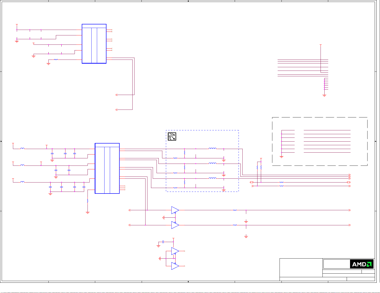
8
7
(07) JUNIPER DAC1 and DAC2
6
5
4
3
2
1
+VDD12DI
+VDD12DI
D D
C C
+AVDD_DAC12
R1500 499RR1500 499R
+AVDD_DAC12
RSET
U1H
U1H
PART 8 OF 15
PART 8 OF 15
AC33
VDD1DI
AC34
VSS1DI
AD34
AVDD
AE34
AVSSQ
AB34
RSET
JUNIPER XT A12 HF MVD SLT BIN1 TSMC FB12
JUNIPER XT A12 HF MVD SLT BIN1 TSMC FB12
R
RB
G
D
D
GB
A
A
C
C
1
1
BB
HSYNC
VSYNC
AD39
AD37
AE36
AD35
AF37
B
AE38
AC36
H1SYNC
AC38
V1SYNC
H1SYNCp.6
V1SYNCp.6
A_R_DAC2_F
A_G_DAC2_F
A_B_DAC2_F
DDCDATA_DAC2_R
DDCCLK_DAC2_R
HSYNC_DAC2_R
VSYNC_DAC2_R
+5V_VESA
DDC2_MONID0
DDC2_MONID2
OPTIONALESDPROTECTIONDIODES
A_R_DAC2_F
SeeBOMforqualifiedfilters
Pseudo differential RGB should be routed from the ASIC to the display
+1.8V
B1600 BLM15AG121SN1DB1600 BLM15AG121SN1D L1600
+1.8V
B1601 BLM15AG121SN1DB1601 BLM15AG121SN1D
B B
+3.3V_BUS
B1602 BLM15AG121SN1DB1602 BLM15AG121SN1D
A A
8
+VDD12DI
1uF_6.3V
1uF_6.3V
+AVDD_DAC12
C1611
C1611
4.7uF_6.3V
4.7uF_6.3V
C1600
C1600
1uF_6.3V
1uF_6.3V
C1607
C1607
100nF_6.3V
100nF_6.3V
C1612
C1612
1uF_6.3V
1uF_6.3V
C1601
C1601
C1608
C1608
100nF_6.3V
100nF_6.3V
C1602
C1602
C1613
C1613
100nF_6.3V
100nF_6.3V
10nF
10nF
+VDD12DI
+AVDD_DAC12
+A2VDD
C1614
C1614
7
10nF
10nF
U1I
U1I
PART 9 OF 15
PART 9 OF 15
AG31
VDD2DI
AG32
VSS2DI
D
AD33
AF33
AG33
AA29
R2SET
R1600
R1600
715R
715R
D
A2VDDQ
A
A
C
C
A2VSSQ
2
2
/
/
T
T
H2SYNC
V
V
A2VDD
R2SET
JUNIPER XT A12 HF MVD SLT BIN1 TSMC FB12
JUNIPER XT A12 HF MVD SLT BIN1 TSMC FB12
V2SYNC
COMP
AC30
R_DAC2
R2
AC31
RB_DAC2
R2B
AD30
G_DAC2
G2
AD31
GB_DAC2
G2B
AF30
B_DAC2
B2
AF31
BB_DAC2
B2B
AD29
AC29
V2SYNC
AD32
Y
AC32
C
AF32
H2SYNCp.6
V2SYNCp.6
100nF_6.3V
100nF_6.3V
6
connector without switching reference plane or running over split plane.
R1601
R1601
75R
75R
402
R1602 37.4RR1602 37.4R
R1608 37.4RR1608 37.4R
R1613 37.4RR1613 37.4R
12 11
9 8
+5V_VESA
C1514
C1514
2 3
5 6
5
13
10
14
1
7
4
U1500D
U1500D
74VHCT125
74VHCT125
74VHCT125
74VHCT125
U1500C
U1500C
U1500A
U1500A
74VHCT125
74VHCT125
74VHCT125
74VHCT125
U1500B
U1500B
402
R1604
R1604
75R
75R
402 402
402
R1609
R1609
75R
75R
402 402
402
HSYNC_DAC2_B
VSYNC_DAC2_B
L1600
L1602
L1602
L1601
L1601
47nH
47nH
402
47nH
47nH
47nH
47nH
4
R1614
R1614
R1615
R1615
DDC4DATAp.8
DDC4CLKp.8
402
24R
24R
DNI
402
24R
24R
DNI
+5V_VESA
R1605
R1605
R1606
R1606
2.2K
2.2K
2.2K
2.2K
A_R_DAC2_F
A_G_DAC2_FH2SYNC
A_B_DAC2_F
R1610 33RR1610 33R
R1612 33RR1612 33R
HSYNC_DAC2_R HSYNC_DAC2_R
VSYNC_DAC2_R VSYNC_DAC2_R
CONFIDENTIAL & PROPRIETARY TO ADVANCED MICRO DEVICES INC.
CONFIDENTIAL & PROPRIETARY TO ADVANCED MICRO DEVICES INC.
CONFIDENTIAL & PROPRIETARY TO ADVANCED MICRO DEVICES INC.
© 2007 Advanced Micro Devices
© 2007 Advanced Micro Devices
© 2007 Advanced Micro Devices
This AMD Board schematic and design is the exclusive property of AMD,
This AMD Board schematic and design is the exclusive property of AMD,
This AMD Board schematic and design is the exclusive property of AMD,
and is provided only to entities under a non-disclosure agreement
and is provided only to entities under a non-disclosure agreement
and is provided only to entities under a non-disclosure agreement
with AMD for evaluation purposes. Further distribution or disclosure
with AMD for evaluation purposes. Further distribution or disclosure
with AMD for evaluation purposes. Further distribution or disclosure
is strictly prohibited. Use of this schematic and design for any purpose
is strictly prohibited. Use of this schematic and design for any purpose
is strictly prohibited. Use of this schematic and design for any purpose
other than evaluation requires a Board Technology License Agreement
other than evaluation requires a Board Technology License Agreement
other than evaluation requires a Board Technology License Agreement
with AMD. AMD makes no representations or warranties of any kind
with AMD. AMD makes no representations or warranties of any kind
with AMD. AMD makes no representations or warranties of any kind
regarding this schematic and design, including, not limited to,
regarding this schematic and design, including, not limited to,
regarding this schematic and design, including, not limited to,
any implied warranty of merchantibility or fitness for a particular
any implied warranty of merchantibility or fitness for a particular
any implied warranty of merchantibility or fitness for a particular
purpose, and disclaims responsibility forany consequences resulting
purpose, and disclaims responsibility forany consequences resulting
purpose, and disclaims responsibility forany consequences resulting
from use of the information included herein.
from use of the information included herein.
from use of the information included herein.
Title
Title
Title
RH JUNIPER GDDR5 1GB DP+DP/HDMI+DVI /sVGA
RH JUNIPER GDDR5 1GB DP+DP/HDMI+DVI /sVGA
3
RH JUNIPER GDDR5 1GB DP+DP/HDMI+DVI /sVGA
DDCDATA_DAC2_R
DDCCLK_DAC2_R
2
A_G_DAC2_F
A_B_DAC2_F
DDCDATA_DAC2_R
DDCCLK_DAC2_R
HSYNC_DAC2_R
VSYNC_DAC2_R
Advanced Micro Devices Inc.
Advanced Micro Devices Inc.
Advanced Micro Devices Inc.
1 Commerce Valley Drive East
1 Commerce Valley Drive East
1 Commerce Valley Drive East
Markham, Ontario
Markham, Ontario
Markham, Ontario
Tuesday, November 10, 2009
Tuesday, November 10, 2009
Tuesday, November 10, 2009
Sheet
Sheet
Sheet
of
721
of
721
of
721
A_R_DAC2_F p.8
A_G_DAC2_F p.8
A_B_DAC2_F p.8
DDCDATA_DAC2_R p.8
DDCCLK_DAC2_R p.8
HSYNC_DAC2_R p.8
VSYNC_DAC2_R p.8
Doc No.
Doc No.
Doc No.
102-C01301-00
102-C01301-00
102-C01301-00
1
RevDate:
RevDate:
RevDate:
50
50
50
Page 8

8
7
(08) JUNIPER TMDP A&B dDVI-I TOP
6
5
4
3
2
1
U1J
+1.8V
B1700 BLM15AG121SN1DB1700 BLM15AG121SN1D
D D
Pleasepayattentiontothegrounding
strategiesforthesefiltercapacitorsto
maintainacloseloopforcurrent.
+1V
B1701 BLM15AG121SN1DB1701 BLM15AG121SN1D
C1713
C1713
C1714
C1717
C1717
C1714
1uF_6.3V
1uF_6.3V
C1718
C1718
1uF_6.3V
1uF_6.3V
4.7uF_6.3V
4.7uF_6.3V
4.7uF_6.3V
4.7uF_6.3V
C C
B B
R1700150R R1700150R
+DPAB_18
GND
+DPAB_18
GND
+DPAB_VDD10
+DPAB_18
DPAB_CALR
U1J
AU28
AV27
AV29
AR28
AP31
AP32
AN33
AP33
AN24
AP24
AP25
AP26
AW28
AN27
AP27
AP28
AW24
AW26
AN29
AP29
AP30
AW30
AW32
JUNIPER XT A12 HF MVD SLT BIN1 TSMC FB12
JUNIPER XT A12 HF MVD SLT BIN1 TSMC FB12
DPA_PVDD
DPA_PVSS
DPB_PVDD
DPB_PVSS
DPA_VDD10#1
DPA_VDD10#2
DPB_VDD10#1
DPB_VDD10#2
DPA_VDD18#1
DPA_VDD18#2
DPB_VDD18#1
DPB_VDD18#2
DPAB_CALR
DPA_VSSR#1
DPA_VSSR#2
DPA_VSSR#3
DPA_VSSR#4
DPA_VSSR#5
DPB_VSSR#1
DPB_VSSR#2
DPB_VSSR#3
DPB_VSSR#4
DPB_VSSR#5
PART 10 OF 15
PART 10 OF 15
T
T
M
M
D
D
P
P
A
A
/
/
B
B
TXCAP_DPA3P
TXCAM_DPA3N
TXCBP_DPB3P
TXCBM_DPB3N
DDCCLK_AUX4P
DDCDATA_AUX4N
OPTIONALESDPROTECTIONDIODES
TX2P_DPA0P
TX2M_DPA0N
TX1P_DPA1P
TX1M_DPA1N
TX0P_DPA2P
TX0M_DPA2N
AUX1P
AUX1N
DDC1CLK
DDC1DATA
TX5P_DPB0P
TX5M_DPB0N
TX4P_DPB1P
TX4M_DPB1N
TX3P_DPB2P
TX3M_DPB2N
ABTX2P
ABTX2M
ABTX1P
ABTX1M
ABTX0P
ABTX0M
ABTXCP
ABTXCM
ABTX5P
ABTX5M
ABTX4P
ABTX4M
ABTX3P
ABTX3M
AT27
DPA_TX2P
DPA_TX2N
DPA_TX1P
DPA_TX0P
DPA_TX0N
DPA_TXCAP
DPA_TXCAN
C1701 100nF_6.3VC1701 100nF_6.3V
C1705 100nF_6.3VC1705 100nF_6.3V
C1706 100nF_6.3VC1706 100nF_6.3V
C1707 100nF_6.3VC1707 100nF_6.3V
C1708 100nF_6.3VC1708 100nF_6.3V
C1709 100nF_6.3VC1709 100nF_6.3V
C1710 100nF_6.3VC1710 100nF_6.3V
C1711 100nF_6.3VC1711 100nF_6.3V
C1720 100nF_6.3VC1720 100nF_6.3V
C1722 100nF_6.3VC1722 100nF_6.3V
C1724 100nF_6.3VC1724 100nF_6.3V
DDC4CLK p.7
DDC4DATA p.7
AR26
AU26
AV25
AT25
AR24
AU24
AV23
AM27
AL27
AM26
AN26
DDCDATA_AUX5Np.9
DDCCLK_AUX5Pp.9
AT33
DPB_TX5P
AU32
DPB_TX5N ABTX5M
AR32
DPB_TX4P
AT31
DPB_TX4N
AV31
DPB_TX3P
AU30
DPB_TX3N
AR30
AT29
AL29
DDC4CLK
AM29
DDC4DATA
SEEBOMFORQUALIFIEDPARTS
DDCDATA_AUX5N
DDCCLK_AUX5P
C1721 100nF_6.3VC1721 100nF_6.3V
C1723 100nF_6.3VC1723 100nF_6.3V
C1725 100nF_6.3VC1725 100nF_6.3V
R1701 499RR1701 499R
R1702 499RR1702 499R
R1704 499RR1704 499R
R1706 499RR1706 499R
R18210RR1821
R18200RR1820
0R
0R
R1709 499RR1709 499R
R1710 499RR1710 499R
R1712 499RR1712 499R
+12V_BUS
R1717
R1717
100K
100K
C1727
C1727
100nF
100nF
16V
DVI_EN
DVI_ENp.9
R1703 499RR1703 499R
R1705 499RR1705 499R
R1707 499RR1707 499R
R1708 499RR1708 499R
DPD_AUXP p.9
DPD_AUXN p.9
R1711 499RR1711 499R
R1713 499RR1713 499R
R1714 499RR1714 499R
DPAB_GND
32
Q1700
Q1700
SI2304DS
SI2304DS
1
DDCCLK_DAC2_Rp.7
DDCDATA_DAC2_Rp.7
VSYNC_DAC2_Rp.7
A_R_DAC2_Fp.7
A_G_DAC2_Fp.7
A_B_DAC2_Fp.7
HSYNC_DAC2_Rp.7
+3.3V_BUS
Q1701
Q1701
MMBT3904
MMBT3904
HPD1p.6
2 3
R1716
R1716
10K
10K
1
R1715 10KR1715 10K
ABTX2P
ABTX2M
ABTX1P
ABTX1MDPA_TX1N
ABTX0P
ABTX0M
ABTXCP
ABTXCM
+5V_VESA
C1712
C1712
1UF_16V
1UF_16V
ABTX2M
ABTX2P
ABTX4M
ABTX4P
DDCCLK_DAC2_R
DDCDATA_DAC2_R
VSYNC_DAC2_R
ABTX1M
ABTX1P
ABTX3M
ABTX3P
ABTX0M
ABTX0P
ABTX5M
ABTX5P
ABTXCP
ABTXCM
A_R_DAC2_F
A_G_DAC2_F
A_B_DAC2_F
HSYNC_DAC2_R
HPD_DVIAB
ABTX5P
ABTX4P
ABTX4M
ABTX3P
ABTX3M
J1700
J1700
25
CASE
1
TMDS Data2-
2
TMDS Data2+
3
TMDS Data2/4 Shield
4
TMDS Data4-
5
TMDS Data4+
6
DDC Clock
7
DDC Data
8
Analog VSYNC
9
TMDS Data1-
10
TMDS Data1+
11
TMDS Data1/3 Shield
12
TMDS Data3-
13
TMDS Data3+
14
+5V Power
15
GND (for +5V)
16
Hot Plug Detect
17
TMDS Data0-
18
TMDS Data0+
19
TMDS Data0/5 Shield
20
TMDS Data5-
21
TMDS Data5+
22
TMDS Clock Shield
23
TMDS Clock+
24
TMDS Clock-
C1
Analog Red
C2
Analog Green
C3
Analog Blue
C4
Analog HYNC
C5
Analog GND
C6
Analog GND#C6
26
CASE#26
27
CASE#27
28
CASE#28
29
CASE#29
30
CASE#30
DVI_CONNECTOR
DVI_CONNECTOR
A A
CONFIDENTIAL & PROPRIETARY TO ADVANCED MICRO DEVICES INC.
CONFIDENTIAL & PROPRIETARY TO ADVANCED MICRO DEVICES INC.
CONFIDENTIAL & PROPRIETARY TO ADVANCED MICRO DEVICES INC.
© 2007 Advanced Micro Devices
© 2007 Advanced Micro Devices
© 2007 Advanced Micro Devices
This AMD Board schematic and design is the exclusive property of AMD,
This AMD Board schematic and design is the exclusive property of AMD,
This AMD Board schematic and design is the exclusive property of AMD,
and is provided only to entities under a non-disclosure agreement
and is provided only to entities under a non-disclosure agreement
and is provided only to entities under a non-disclosure agreement
with AMD for evaluation purposes. Further distribution or disclosure
with AMD for evaluation purposes. Further distribution or disclosure
with AMD for evaluation purposes. Further distribution or disclosure
is strictly prohibited. Use of this schematic and design for any purpose
is strictly prohibited. Use of this schematic and design for any purpose
is strictly prohibited. Use of this schematic and design for any purpose
other than evaluation requires a Board Technology License Agreement
other than evaluation requires a Board Technology License Agreement
other than evaluation requires a Board Technology License Agreement
with AMD. AMD makes no representations or warranties of any kind
with AMD. AMD makes no representations or warranties of any kind
with AMD. AMD makes no representations or warranties of any kind
regarding this schematic and design, including, not limited to,
regarding this schematic and design, including, not limited to,
regarding this schematic and design, including, not limited to,
any implied warranty of merchantibility or fitness for a particular
any implied warranty of merchantibility or fitness for a particular
any implied warranty of merchantibility or fitness for a particular
purpose, and disclaims responsibility forany consequences resulting
purpose, and disclaims responsibility forany consequences resulting
purpose, and disclaims responsibility forany consequences resulting
from use of the information included herein.
from use of the information included herein.
from use of the information included herein.
Title
Title
Title
RH JUNIPER GDDR5 1GB DP+DP/HDMI+DVI /sVGA
RH JUNIPER GDDR5 1GB DP+DP/HDMI+DVI /sVGA
8
7
6
5
4
3
RH JUNIPER GDDR5 1GB DP+DP/HDMI+DVI /sVGA
2
Advanced Micro Devices Inc.
Advanced Micro Devices Inc.
Advanced Micro Devices Inc.
1 Commerce Valley Drive East
1 Commerce Valley Drive East
1 Commerce Valley Drive East
Markham, Ontario
Markham, Ontario
Markham, Ontario
Tuesday, November 10, 2009
Tuesday, November 10, 2009
Tuesday, November 10, 2009
Sheet
Sheet
Sheet
of
821
of
821
of
821
Doc No.
Doc No.
Doc No.
1
RevDate:
RevDate:
RevDate:
50
50
50
102-C01301-00
102-C01301-00
102-C01301-00
Page 9

8
7
6
5
4
3
2
1
(09) JUNIPER Display Port C & Display Port/HDMI D
AUX/DDC:
D D
+1.8V
B1800 BLM15AG121SN1DB1800 BLM15AG121SN1D
C1803
C1803
1uF_6.3V
1uF_6.3V
Pleasepayattentiontothegrounding
strategiesforthesefiltercapacitorsto
maintainacloseloopforcurrent.
+1V
B1801 BLM15AG121SN1DB1801 BLM15AG121SN1D
4.7uF_6.3V
4.7uF_6.3V
C C
4.7uF_6.3V
4.7uF_6.3V
B B
C1819
C1819
C1813
C1813
1uF_6.3V
1uF_6.3V
C1820
C1820
1uF_6.3V
1uF_6.3V
C1814
C1814
R1800150R R1800150R
+DPCD_18
GND
+DPCD_18
GND
+DPCD_VDD10
+DPCD_18
DPCD_CALR
U1K
U1K
AU18
AV17
AV19
AR18
AP13
AT13
AP14
AP15
AP20
AP21
AP22
AP23
AW18
AN17
AP16
AP17
AW14
AW16
AN19
AP18
AP19
AW20
AW22
JUNIPER XT A12 HF MVD SLT BIN1 TSMC FB12
JUNIPER XT A12 HF MVD SLT BIN1 TSMC FB12
DPC_PVDD
DPC_PVSS
DPD_PVDD
DPD_PVSS
DPC_VDD10#1
DPC_VDD10#2
DPD_VDD10#1
DPD_VDD10#2
DPC_VDD18#1
DPC_VDD18#2
DPD_VDD18#1
DPD_VDD18#2
DPCD_CALR
DPC_VSSR#1
DPC_VSSR#2
DPC_VSSR#3
DPC_VSSR#4
DPC_VSSR#5
DPD_VSSR#1
DPD_VSSR#2
DPD_VSSR#3
DPD_VSSR#4
DPD_VSSR#5
PART 11 OF 15
PART 11 OF 15
T
T
M
M
D
D
P
P
C
C
/
/
D
D
TX2P_DPC0P
TX2M_DPC0N
TX1P_DPC1P
TX1M_DPC1N
TX0P_DPC2P
TX0M_DPC2N
TXCCP_DPC3P
TXCCM_DPC3N
AUX2P
AUX2N
DDC2CLK
DDC2DATA
TX5P_DPD0P
TX5M_DPD0N
TX4P_DPD1P
TX4M_DPD1N
TX3P_DPD2P
TX3M_DPD2N
TXCDP_DPD3P
TXCDM_DPD3N
DDCCLK_AUX5P
DDCDATA_AUX5N
AT17
DPC_C0P
AR16
DPC_C0N
AU16
DPC_C1P
AV15
DPC_C1N
AT15
DPC_C2P
AR14
DPC_C2N
AU14
DPC_C3P DPC_3P
AV13
DPC_C3N
AN20
AUX2P
AM20
AUX2N
AM19
DDC2CLK
AL19
DDC2DATA
AT23
DPD_C0P
AR22
DPD_C0N
AU22
DPD_C1P
AV21
DPD_C1N
AT21
DPD_C2P
AR20
DPD_C2N
AU20
DPD_C3P
AT19
DPD_C3N
AN21
DDCCLK_AUX5P
AM21
DDCDATA_AUX5N
+5V
AUX2PAUX2P
DPC_AUXN
DDCCLK_AUX5P p.8
DDCDATA_AUX5N p.8
DPD_AUXN
C1801 100nF_6.3VC1801 100nF_6.3V
C1802 100nF_6.3VC1802 100nF_6.3V
C1805 100nF_6.3VC1805 100nF_6.3V
C1806 100nF_6.3VC1806 100nF_6.3V
C1807 100nF_6.3VC1807 100nF_6.3V
C1808 100nF_6.3VC1808 100nF_6.3V
C1809 100nF_6.3VC1809 100nF_6.3V
C1810 100nF_6.3VC1810 100nF_6.3V
C1811 100nF_6.3VC1811 100nF_6.3V
C1812 100nF_6.3VC1812 100nF_6.3V
C1822 100nF_6.3VC1822 100nF_6.3V
C1823 100nF_6.3VC1823 100nF_6.3V
C1824 100nF_6.3VC1824 100nF_6.3V
C1825 100nF_6.3VC1825 100nF_6.3V
C1826 100nF_6.3VC1826 100nF_6.3V
C1827 100nF_6.3VC1827 100nF_6.3V
C1828 100nF_6.3VC1828 100nF_6.3V
C1829 100nF_6.3VC1829 100nF_6.3V
DDCCLK_AUX5P
DDC2DATA
DDC2CLK
OPTIONALESDprotectiondiodes
DPC_3N
DPC_3P
DPC_2N
DPC_2P
DPC_1P
DPC_0N
DPC_0P
A A
8
DPC_3N
DPC_3P
DPC_2N
DPC_2P
DPC_1NDPC_1N
DPC_1P
DPC_0N
DPC_0P
7
DPD_3N
DPD_3P
DPD_2N
DPD_2P
DPD_1N
DPD_1P
DPD_0N
DPD_0P
DPC_AUXN
DPC_AUXP
DPD_AUXN
DPD_AUXP
DPC_DONGLE_DET
DPD_DONGLE_DET
6
DPD_3N
DPD_3P
DPD_2N
DPD_2P
DPD_1N
DPD_1P
DPD_0N
DPD_0P
5
FOR740/730,INSTALL0RONASIC‐SIDEOFACCOUPLINGCAPSONLY;
FORJUNIPER,INSTALL0RONCONNECTORSIDEOFACCOUPLINGCAPSONLY;
DPC_AUXP
DPC_AUXN
R18160RR1816
R18170RR1817
0R
+5V_HDMI
DDCDATA_AUX5N
GPIO_14_HPD2p.6
+5V
R1831 2.2KR1831 2.2K
1
DPC_DONGLE_DET
R1832 2.2KR1832 2.2K
DPD_DONGLE_DET
DPD_0P
DPD_0N
DPD_1P
DPD_1N
DPD_2P
DPD_2N
DPD_3P
DPD_3N
DPD_GND
32
GENERICE_HPD4p.6
GENERICF_HPD5p.6
DNI‐FORTESTONLY
Q1802
Q1802
SI2304DS
SI2304DS
R1822
R1822
499R
499R
DPC_AUXP
AUX2N
DPD_AUXPp.8
DPD_AUXNp.8
0R
DETC_BUF
DVI_ENp.8
DETD_BUF
DPD_AUXP
4
J1800
J1800
DPC_1M
R18061MR1806
1M
DPD_1M
+5V_HDMI
1
ML_Lane_0p
2
GND_0
3
ML_Lane_0n
4
ML_Lane_1p
5
GND_1
6
ML_Lane_1n
7
ML_Lane_2p
8
GND_2
9
ML_Lane_2n
10
ML_Lane_3p
11
GND_3
12
ML_Lane_3n
13
Pin_13
14
Pin_14
15
AUX_CHp
16
GND_6
17
AUX_CHn
18
Hot_Det
20
DP_PWR
PWR_RTN19G1
DISPLAYPORT
DISPLAYPORT
MJ1801
MJ1801
1
1
GND#20
2
2
GND#21
3
3
GND#22
4
4
GND#23
5
5
6
6
7
7
8
8
9
9
10
10
11
11
12
12
13
13
14
14
15
15
16
16
17
17
18
18
19
19
LONG_TYPE-2_HDMI
LONG_TYPE-2_HDMI
G4
G4
G3
G3
G2
G2
G1
20
21
22
23
R1823
R1823
499R
499R
Q1800
Q1800
MMBT3904
MMBT3904
Q1801
Q1801
MMBT3904
MMBT3904
R1824
R1824
499R
499R
+3.3V_BUS
2 3
R1808
R1808
10K
10K
+3.3V_BUS
2 3
R1815
R1815
10K
10K
R1825
R1825
499R
499R
DPC_0P
DPC_0N
DPC_1P
DPC_1N
DPC_2P
DPC_2N
DPC_3N
R1801 1MR1801 1M
R1802 100KR1802 100K
R1803 100KR1803 100K
F1800
F1800
NANOSMDC150F-2
NANOSMDC150F-2
1
10K
10K
R1807
R1807
+3.3V_DP
10K
10K
R1814
R1814
+3.3V_BUS+5V
1
DPC_DONGLE_DET
DPC_AUXP
DPC_AUXN
+3.3V_BUS
HPD_DPC
+3.3V_DP+3.3V_BUS
C1817
C1817
10uF
10uF
DPD_0P
DPD_0N
DPD_1P
DPD_1N
DPD_2P
DPD_2N
DPD_3P
DPD_3N
DPD_DONGLE_DET
DPD_AUXP
DPD_AUXN
+3.3V_BUS
HPD_DPD
+3.3V_DPD
Share PADs
DPD_0P
DPD_0N
DPD_1P
DPD_1N
DPD_2P
DPD_2N
DPD_3P
DPD_3N
CEC1
DPD_AUXP
R1826
R1826
499R
499R
R1827
R1827
499R
499R
R1828
R1828
499R
499R
R1829
R1829
499R
499R
DPD_AUXN
HPD_DPD
C1834
C1834
1uF_6.3V
1uF_6.3V
OVERLAPHDMIWITHDPD
CONFIDENTIAL & PROPRIETARY TO ADVANCED MICRO DEVICES INC.
CONFIDENTIAL & PROPRIETARY TO ADVANCED MICRO DEVICES INC.
CONFIDENTIAL & PROPRIETARY TO ADVANCED MICRO DEVICES INC.
© 2007 Advanced Micro Devices
© 2007 Advanced Micro Devices
© 2007 Advanced Micro Devices
This AMD Board schematic and design is the exclusive property of AMD,
This AMD Board schematic and design is the exclusive property of AMD,
This AMD Board schematic and design is the exclusive property of AMD,
and is provided only to entities under a non-disclosure agreement
and is provided only to entities under a non-disclosure agreement
and is provided only to entities under a non-disclosure agreement
with AMD for evaluation purposes. Further distribution or disclosure
with AMD for evaluation purposes. Further distribution or disclosure
with AMD for evaluation purposes. Further distribution or disclosure
is strictly prohibited. Use of this schematic and design for any purpose
is strictly prohibited. Use of this schematic and design for any purpose
is strictly prohibited. Use of this schematic and design for any purpose
other than evaluation requires a Board Technology License Agreement
other than evaluation requires a Board Technology License Agreement
other than evaluation requires a Board Technology License Agreement
with AMD. AMD makes no representations or warranties of any kind
with AMD. AMD makes no representations or warranties of any kind
with AMD. AMD makes no representations or warranties of any kind
regarding this schematic and design, including, not limited to,
regarding this schematic and design, including, not limited to,
regarding this schematic and design, including, not limited to,
any implied warranty of merchantibility or fitness for a particular
any implied warranty of merchantibility or fitness for a particular
any implied warranty of merchantibility or fitness for a particular
purpose, and disclaims responsibility forany consequences resulting
purpose, and disclaims responsibility forany consequences resulting
purpose, and disclaims responsibility forany consequences resulting
from use of the information included herein.
from use of the information included herein.
from use of the information included herein.
Title
Title
Title
RH JUNIPER GDDR5 1GB DP+DP/HDMI+DVI /sVGA
RH JUNIPER GDDR5 1GB DP+DP/HDMI+DVI /sVGA
3
RH JUNIPER GDDR5 1GB DP+DP/HDMI+DVI /sVGA
2
Advanced Micro Devices Inc.
Advanced Micro Devices Inc.
Advanced Micro Devices Inc.
1 Commerce Valley Drive East
1 Commerce Valley Drive East
1 Commerce Valley Drive East
Markham, Ontario
Markham, Ontario
Markham, Ontario
Tuesday, November 10, 2009
Tuesday, November 10, 2009
Tuesday, November 10, 2009
Sheet
Sheet
Sheet
of
921
of
921
of
921
Doc No.
Doc No.
Doc No.
1
RevDate:
RevDate:
RevDate:
50
50
50
102-C01301-00
102-C01301-00
102-C01301-00
Page 10

8
7
6
5
4
3
2
1
(10) JUNIPER LVTMDP E&F
U1L
+1.8V
B1900 BLM15AG121SN1DB1900 BLM15AG121SN1D
D D
+1V
B1901 BLM15AG121SN1DB1901 BLM15AG121SN1D
C C
+DPEF_18
GND
+DPEF_18
GND
+DPEF_VDD10
+DPEF_18
DPEF_CALR
R1900150R R1900150R
U1L
AM37
AN38
AL38
AM35
AL33
AM33
AK33
AK34
AH34
AJ34
AF34
AG34
AM39
AN34
AP39
AR39
AU37
AF39
AH39
AK39
AL34
AM34
JUNIPER XT A12 HF MVD SLT BIN1 TSMC FB12
JUNIPER XT A12 HF MVD SLT BIN1 TSMC FB12
DPE_PVDD
DPE_PVSS
DPF_PVDD
DPF_PVSS
DPE_VDD10#1
DPE_VDD10#2
DPF_VDD10#1
DPF_VDD10#2
DPE_VDD18#1
DPE_VDD18#2
DPF_VDD18#1
DPF_VDD18#2
DPEF_CALR
DPE_VSSR#1
DPE_VSSR#2
DPE_VSSR#3
DPE_VSSR#4
DPF_VSSR#1
DPF_VSSR#2
DPF_VSSR#3
DPF_VSSR#4
DPF_VSSR#5
PART 12 OF 15
PART 12 OF 15
L
L
V
V
T
T
M
M
D
D
P
P
E
E
/
/
F
F
DDCDATA_AUX3N
DDCDATA_AUX7N
T2X2P_DPE0P
T2X2M_DPE0N
T2X1P_DPE1P
T2X1M_DPE1N
T2X0P_DPE2P
T2X0M_DPE2N
T2XCEP_DPE3P
T2XCEM_DPE3N
DDCCLK_AUX3P
T2X5P_DPF0P
T2X5M_DPF0N
T2X4P_DPF1P
T2X4M_DPF1N
T2X3P_DPF2P
T2X3M_DPF2N
T2XCFP_DPF3P
T2XCFM_DPF3N
DDCCLK_AUX7P
AP35
AR35
AR37
AU39
AW37
AU35
AP34
AR34
AL30
AM30
5VTOLERANT
AG38
AH37
AH35
AJ36
AJ38
AK37
AK35
AL36
AK30
AK29
B B
A A
CONFIDENTIAL & PROPRIETARY TO ADVANCED MICRO DEVICES INC.
CONFIDENTIAL & PROPRIETARY TO ADVANCED MICRO DEVICES INC.
CONFIDENTIAL & PROPRIETARY TO ADVANCED MICRO DEVICES INC.
© 2007 Advanced Micro Devices
© 2007 Advanced Micro Devices
© 2007 Advanced Micro Devices
This AMD Board schematic and design is the exclusive property of AMD,
This AMD Board schematic and design is the exclusive property of AMD,
This AMD Board schematic and design is the exclusive property of AMD,
and is provided only to entities under a non-disclosure agreement
and is provided only to entities under a non-disclosure agreement
and is provided only to entities under a non-disclosure agreement
with AMD for evaluation purposes. Further distribution or disclosure
with AMD for evaluation purposes. Further distribution or disclosure
with AMD for evaluation purposes. Further distribution or disclosure
is strictly prohibited. Use of this schematic and design for any purpose
is strictly prohibited. Use of this schematic and design for any purpose
is strictly prohibited. Use of this schematic and design for any purpose
other than evaluation requires a Board Technology License Agreement
other than evaluation requires a Board Technology License Agreement
other than evaluation requires a Board Technology License Agreement
with AMD. AMD makes no representations or warranties of any kind
with AMD. AMD makes no representations or warranties of any kind
with AMD. AMD makes no representations or warranties of any kind
regarding this schematic and design, including, not limited to,
regarding this schematic and design, including, not limited to,
regarding this schematic and design, including, not limited to,
any implied warranty of merchantibility or fitness for a particular
any implied warranty of merchantibility or fitness for a particular
any implied warranty of merchantibility or fitness for a particular
purpose, and disclaims responsibility forany consequences resulting
purpose, and disclaims responsibility forany consequences resulting
purpose, and disclaims responsibility forany consequences resulting
from use of the information included herein.
from use of the information included herein.
from use of the information included herein.
Title
Title
Title
RH JUNIPER GDDR5 1GB DP+DP/HDMI+DVI /sVGA
RH JUNIPER GDDR5 1GB DP+DP/HDMI+DVI /sVGA
8
7
6
5
4
3
RH JUNIPER GDDR5 1GB DP+DP/HDMI+DVI /sVGA
2
Advanced Micro Devices Inc.
Advanced Micro Devices Inc.
Advanced Micro Devices Inc.
1 Commerce Valley Drive East
1 Commerce Valley Drive East
1 Commerce Valley Drive East
Markham, Ontario
Markham, Ontario
Markham, Ontario
Tuesday, November 10, 2009
Tuesday, November 10, 2009
Tuesday, November 10, 2009
Sheet
Sheet
Sheet
of
10 21
of
10 21
of
10 21
Doc No.
Doc No.
Doc No.
1
RevDate:
RevDate:
RevDate:
50
50
50
102-C01301-00
102-C01301-00
102-C01301-00
Page 11

5
(11) JUNIPER Power & GND
4
3
2
1
C1213
C1213
1uF_6.3V
1uF_6.3V
C1218
C1218
1uF_6.3V
1uF_6.3V
C1265
C1265
1uF_6.3V
1uF_6.3V
C1235
C1235
47uF_2.5V
47uF_2.5V
C1240
C1240
22uF
22uF
+VDDC
U1M
+MVDD
C1269
C1241
C1241
C1245
100nF_6.3V
100nF_6.3V
C1222
C1222
1uF_6.3V
1uF_6.3V
C1244
C1244
1uF_6.3V
1uF_6.3V
C1206
C1206
1uF_6.3V
1uF_6.3V
C1230
C1230
2.2UF_2.5V
2.2UF_2.5V
C1245
100nF_6.3V
100nF_6.3V
C1233
C1233
1uF_6.3V
1uF_6.3V
C1228
C1228
2.2UF_2.5V
2.2UF_2.5V
C1268
C1229
C1229
100nF_6.3V
100nF_6.3V
C1252
C1252
100nF_6.3V
100nF_6.3V
C1214
C1214
1uF_6.3V
1uF_6.3V
C1254
C1254
2.2UF_2.5V
2.2UF_2.5V
MC1270
MC1270
10uF
10uF
C1268
100nF_6.3V
100nF_6.3V
C1209
C1209
1uF_6.3V
1uF_6.3V
C1243
C1243
1uF_6.3V
1uF_6.3V
C1255
C1255
2.2UF_2.5V
2.2UF_2.5V
C1227
C1227
C1200
D D
C C
C1200
100nF_6.3V
100nF_6.3V
C1251
C1251
100nF_6.3V
100nF_6.3V
C1201
C1201
1uF_6.3V
1uF_6.3V
C1208
C1208
2.2UF_2.5V
2.2UF_2.5V
C1234
C1234
2.2UF_2.5V
2.2UF_2.5V
MC1266
MC1266
10uF
10uF
100nF_6.3V
100nF_6.3V
C1253
C1253
100nF_6.3V
100nF_6.3V
C1242
C1242
1uF_6.3V
1uF_6.3V
C1231
C1231
2.2UF_2.5V
2.2UF_2.5V
C1232
C1232
2.2UF_2.5V
2.2UF_2.5V
MC1267
MC1267
10uF
10uF
C1271
C1271
100nF_6.3V
100nF_6.3V
C1256
C1256
1uF_6.3V
1uF_6.3V
C1202
C1202
1uF_6.3V
1uF_6.3V
C1269
100nF_6.3V
100nF_6.3V
C1221
C1221
1uF_6.3V
1uF_6.3V
C1207
C1207
1uF_6.3V
1uF_6.3V
C1257
C1257
2.2UF_2.5V
2.2UF_2.5V
Overlap cap pair foorprints (0805 with 0603)
+1.8V
C31
C31
C30
C30
1uF_6.3V
C1304
C1304
1uF_6.3V
1uF_6.3V
C1307
C1307
22uF
22uF
1uF_6.3V
C1303
C1303
1uF_6.3V
1uF_6.3V
+VDDCI
C1294
C1294
C1289
C1289
C1288
C1288
1uF_6.3V
1uF_6.3V
C1299
C1313
C1313
22uF
22uF
C1299
1uF_6.3V
1uF_6.3V
C1314
C1314
22uF
22uF
B B
0805
4V
X6S
1uF_6.3V
1uF_6.3V
C1300
C1300
1uF_6.3V
1uF_6.3V
C1315
C1315
22uF
22uF
1uF_6.3V
1uF_6.3V
C1302
C1302
1uF_6.3V
1uF_6.3V
C1285
C1285
22uF
22uF
C1306
C1306
1uF_6.3V
1uF_6.3V
C1316
C1316
22uF
22uF
C1311
C1311
1uF_6.3V
1uF_6.3V
C1301
C1301
22uF
22uF
C1310
C1310
1uF_6.3V
1uF_6.3V
C1305
C1305
22uF
22uF
1uF_6.3V
1uF_6.3V
C1291
C1291
1uF_6.3V
1uF_6.3V
C32
C32
100nF_6.3V
100nF_6.3V
U1M
PART 13 OF 15
PART 13 OF 15
AC7
VDDR1#1
AD11
VDDR1#2
AF7
VDDR1#3
AG10
VDDR1#4
AJ7
VDDR1#5
AK8
VDDR1#6
AL9
VDDR1#7
G11
VDDR1#8
G14
VDDR1#9
G17
VDDR1#10
G20
VDDR1#11
G23
VDDR1#12
G26
VDDR1#13
G29
VDDR1#14
H10
VDDR1#15
J7
VDDR1#16
J9
VDDR1#17
K11
VDDR1#18
K13
VDDR1#19
K8
VDDR1#20
L12
VDDR1#21
L16
VDDR1#22
L21
VDDR1#23
L23
VDDR1#24
L26
VDDR1#25
L7
VDDR1#26
M11
VDDR1#27
N11
VDDR1#28
P7
VDDR1#29
R11
VDDR1#30
U11
VDDR1#31
U7
VDDR1#32
Y11
VDDR1#33
Y7
VDDR1#34
M20
NC_VDDRHA
M21
NC_VSSRHA
V12
NC_VDDRHB
U12
NC_VSSRHB
AF26
VDD_CT#1
AF27
VDD_CT#2
AG26
VDD_CT#3
AG27
VDD_CT#4
AA13
VDDCI#1
AB13
VDDCI#2
AC12
VDDCI#3
AC15
VDDCI#4
AD13
VDDCI#5
AD16
VDDCI#6
M15
VDDCI#7
M16
VDDCI#8
M18
VDDCI#9
M23
VDDCI#10
N13
VDDCI#11
N15
VDDCI#12
N17
VDDCI#13
N20
VDDCI#14
N22
VDDCI#15
R12
VDDCI#16
R13
VDDCI#17
R16
VDDCI#18
T12
VDDCI#19
T15
VDDCI#20
V15
VDDCI#21
Y13
VDDCI#22
AG28
FB_VDDCI
JUNIPER XT A12 HF MVD SLT BIN1 TSMC FB12
JUNIPER XT A12 HF MVD SLT BIN1 TSMC FB12
VDDC#1
VDDC#2
VDDC#3
VDDC#4
VDDC#5
VDDC#6
VDDC#7
VDDC#8
VDDC#9
VDDC#10
VDDC#11
VDDC#12
VDDC#13
VDDC#14
VDDC#15
VDDC#16
VDDC#17
VDDC#18
VDDC#19
VDDC#20
VDDC#21
VDDC#22
VDDC#23
VDDC#24
VDDC#25
VDDC#26
VDDC#27
VDDC#28
P
P
VDDC#29
VDDC#30
O
O
VDDC#31
W
W
VDDC#32
E
E
VDDC#33
VDDC#34
R
R
VDDC#35
VDDC#36
VDDC#37
VDDC#38
VDDC#39
VDDC#40
VDDC#41
VDDC#42
VDDC#43
VDDC#44
VDDC#45
VDDC#46
VDDC#47
VDDC#48
VDDC#49
VDDC#50
VDDC#51
VDDC#52
VDDC#53
VDDC#54
VDDC#55
VDDC#56
VDDC#57
VDDC#58
FB_VDDC
FB_GND
TS_A
AA15
AA17
AA20
AA22
AA24
AA27
AB16
AB18
AB21
AB23
AB26
AB28
AC17
AC20
AC22
AC24
AC27
AD18
AD21
AD23
AD26
AF17
AF20
AF22
AG16
AG18
AG21
AH22
AH27
AH28
M26
N24
N27
R18
R21
R23
R26
T17
T20
T22
T24
T27
U16
U18
U21
U23
U26
V17
V20
V22
V24
V27
Y16
Y18
Y21
Y23
Y26
Y28
AL31
AF28
AH29
0‐1VINPUT
1.8VMAX
TS_A
C1203
C1203
1uF_6.3V
1uF_6.3V
C1210
C1210
1uF_6.3V
1uF_6.3V
C1258
C1258
1uF_6.3V
1uF_6.3V
C1264
C1264
1uF_6.3V
1uF_6.3V
4V,0805FOOTPRINT
C1273
C1273
47uF_2.5V
47uF_2.5V
FB_VDDC p.12
FB_GND p.12
C1224
C1224
1uF_6.3V
1uF_6.3V
C1211
C1211
1uF_6.3V
1uF_6.3V
C1259
C1259
1uF_6.3V
1uF_6.3V
C1220
C1220
1uF_6.3V
1uF_6.3V
C1276
C1276
47uF_2.5V
47uF_2.5V
C1236
C1236
1uF_6.3V
1uF_6.3V
C1247
C1247
1uF_6.3V
1uF_6.3V
C1260
C1260
1uF_6.3V
1uF_6.3V
C1277
C1277
47uF_2.5V
47uF_2.5V
C1237
C1237
1uF_6.3V
1uF_6.3V
C1248
C1248
1uF_6.3V
1uF_6.3V
C1261
C1261
1uF_6.3V
1uF_6.3V
C1282
C1282
47uF_2.5V
47uF_2.5V
+1.8V
R4020
R4020
10K
10K
R4019
R4019
10K
10K
C1238
C1238
1uF_6.3V
1uF_6.3V
C1249
C1249
1uF_6.3V
1uF_6.3V
C1262
C1262
1uF_6.3V
1uF_6.3V
C1284
C1284
47uF_2.5V
47uF_2.5V
DNI
DNI
C1212
C1212
1uF_6.3V
1uF_6.3V
C1215
C1215
1uF_6.3V
1uF_6.3V
C1263
C1263
1uF_6.3V
1uF_6.3V
C1287
C1287
47uF_2.5V
47uF_2.5V
C1239
C1239
1uF_6.3V
1uF_6.3V
C1217
C1217
1uF_6.3V
1uF_6.3V
C1250
C1250
1uF_6.3V
1uF_6.3V
C1283
C1283
47uF_2.5V
47uF_2.5V
U1N
U1N
PART 14 OF 15
PART 14 OF 15
GND#91
GND#92
GND#93
GND#94
GND#95
GND#96
GND#97
GND#98
GND#99
GND#100
GND#101
GND#102
GND#103
GND#104
GND#105
GND#106
GND#107
GND#108
GND#109
GND#110
GND#111
GND#112
GND#113
GND#114
GND#115
J2
GND#116
GND#117
J6
GND#118
J8
GND#119
GND#120
GND#121
GND#122
GND#123
L2
GND#124
GND#125
GND#126
L6
GND#127
GND#128
GND#129
GND#130
GND#131
G
G
GND#132
GND#133
N
N
GND#134
D
D
GND#135
GND#136
GND#137
GND#138
GND#139
GND#140
GND#141
GND#142
GND#143
GND#144
GND#145
GND#146
GND#147
GND#148
GND#149
GND#150
GND#151
GND#152
GND#153
GND#154
GND#155
GND#156
GND#157
GND#158
GND#159
GND#160
GND#161
GND#162
GND#163
GND#164
GND#165
GND#166
GND#167
GND#168
GND#169
GND#170
GND#171
GND#172
GND#173
GND#174
GND#175
GND#176
VSS_MECH#1
VSS_MECH#2
VSS_MECH#3
JUNIPER XT A12 HF MVD SLT BIN1 TSMC FB12
JUNIPER XT A12 HF MVD SLT BIN1 TSMC FB12
AW39
B31
B33
B7
B9
C1
C39
E35
E5
F11
F13
F15
F17
F19
F21
F23
F25
F27
F29
F31
F33
F7
F9
G2
G6
H9
J27
K14
K7
L11
L17
L22
L24
M17
M22
M24
N16
N18
N2
N21
N23
N26
N6
R15
R17
R2
R20
R22
R24
R27
R6
T11
T13
T16
T18
T21
T23
T26
U13
U15
U17
U2
U20
U22
U24
U27
U6
V11
V13
V16
V18
V21
V23
V26
W2
W6
Y15
Y17
Y20
Y22
Y24
Y27
A39
AW1
GND#1
GND#2
GND#3
GND#4
GND#5
GND#6
GND#7
GND#8
GND#9
GND#10
GND#11
GND#12
GND#13
GND#14
GND#15
GND#16
GND#17
GND#18
GND#19
GND#20
GND#21
GND#22
GND#23
GND#24
GND#25
GND#26
GND#27
GND#28
GND#29
GND#30
GND#31
GND#32
GND#33
GND#34
GND#35
GND#36
GND#37
GND#38
GND#39
GND#40
GND#41
GND#42
GND#43
GND#44
GND#45
GND#46
GND#47
GND#48
GND#49
GND#50
GND#51
GND#52
GND#53
GND#54
GND#55
GND#56
GND#57
GND#58
GND#59
GND#60
GND#61
GND#62
GND#63
GND#64
GND#65
GND#66
GND#67
GND#68
GND#69
GND#70
GND#71
GND#72
GND#73
GND#74
GND#75
GND#76
GND#77
GND#78
GND#80
GND#81
GND#82
GND#83
GND#84
GND#85
GND#86
GND#87
GND#88
GND#89
A3
A37
AA16
AA18
AA2
AA21
AA23
AA26
AA28
AA6
AB12
AB15
AB17
AB20
AB22
AB24
AB27
AC11
AC13
AC16
AC18
AC2
AC21
AC23
AC26
AC28
AC6
AD15
AD17
AD20
AD22
AD24
AD27
AD9
AE2
AE6
AF10
AF16
AF18
AF21
AG17
AG2
AG20
AG22
AG6
AG9
AH21
AJ10
AJ11
AJ2
AJ28
AJ6
AK11
AK31
AK7
AL11
AL14
AL17
AL2
AL20
AL21
AL23
AL26
AL32
AL6
AL8
AM11
AM31
AM9
AN11
AN2
AN30
AN6
AN8
AP11
AP7
AP9
AR5
B11
B13
B15
B17
B19
B21
B23
B25
B27
B29
A A
CONFIDENTIAL & PROPRIETARY TO ADVANCED MICRO DEVICES INC.
CONFIDENTIAL & PROPRIETARY TO ADVANCED MICRO DEVICES INC.
CONFIDENTIAL & PROPRIETARY TO ADVANCED MICRO DEVICES INC.
© 2007 Advanced Micro Devices
© 2007 Advanced Micro Devices
© 2007 Advanced Micro Devices
This AMD Board schematic and design is the exclusive property of AMD,
This AMD Board schematic and design is the exclusive property of AMD,
This AMD Board schematic and design is the exclusive property of AMD,
and is provided only to entities under a non-disclosure agreement
and is provided only to entities under a non-disclosure agreement
and is provided only to entities under a non-disclosure agreement
with AMD for evaluation purposes. Further distribution or disclosure
with AMD for evaluation purposes. Further distribution or disclosure
with AMD for evaluation purposes. Further distribution or disclosure
is strictly prohibited. Use of this schematic and design for any purpose
is strictly prohibited. Use of this schematic and design for any purpose
is strictly prohibited. Use of this schematic and design for any purpose
other than evaluation requires a Board Technology License Agreement
other than evaluation requires a Board Technology License Agreement
other than evaluation requires a Board Technology License Agreement
with AMD. AMD makes no representations or warranties of any kind
with AMD. AMD makes no representations or warranties of any kind
with AMD. AMD makes no representations or warranties of any kind
regarding this schematic and design, including, not limited to,
regarding this schematic and design, including, not limited to,
regarding this schematic and design, including, not limited to,
any implied warranty of merchantibility or fitness for a particular
any implied warranty of merchantibility or fitness for a particular
any implied warranty of merchantibility or fitness for a particular
purpose, and disclaims responsibility forany consequences resulting
purpose, and disclaims responsibility forany consequences resulting
purpose, and disclaims responsibility forany consequences resulting
from use of the information included herein.
from use of the information included herein.
from use of the information included herein.
Title
Title
Title
RH JUNIPER GDDR5 1GB DP+DP/HDMI+DVI /sVGA
RH JUNIPER GDDR5 1GB DP+DP/HDMI+DVI /sVGA
5
4
3
2
RH JUNIPER GDDR5 1GB DP+DP/HDMI+DVI /sVGA
Advanced Micro Devices Inc.
Advanced Micro Devices Inc.
Advanced Micro Devices Inc.
1 Commerce Valley Drive East
1 Commerce Valley Drive East
1 Commerce Valley Drive East
Markham, Ontario
Markham, Ontario
Markham, Ontario
Tuesday, November 10, 2009
Tuesday, November 10, 2009
Tuesday, November 10, 2009
Sheet
Sheet
Sheet
of
11 21
of
11 21
of
11 21
1
Doc No.
Doc No.
Doc No.
RevDate:
RevDate:
RevDate:
50
50
50
102-C01301-00
102-C01301-00
102-C01301-00
Page 12

(12) VDDC
8
PHASE 1
7
6
PHASE 2
5
4
3
2
1
PHASE 3
Output Bulk CAPs
+12VBUS_SOURCE
D D
UGATE1_CTR
RC snubber values
shown are for reference
only, tuning is required
C C
+12VEXT_SOURCE
B B
+12VEXT_SOURCE
+12VBUS_SOURCE
A A
UGATE1_1
R601 0RR601 0R
R606
R606
2.2R
2.2R
805
C606
C606
4.7nF
4.7nF
603
Place across
Q603, Q604
LGATE1_CTR LGATE2_CTR LGATE3_CTR
R603 0RR603 0R
MR603
MR603
10K
10K
Circuitry that have to be placed close to the device:
- current sense,
- compensation network,
- thermal compensation network (Droop, OCP, etc)
OPTIONAL
R629 2.2RR629 2.2R
0805
C627
C627
1UF_16V
1UF_16V
R619 2.2RR619 2.2R
C617
C617
OPTIONAL
1UF_16V
1UF_16V
+12V_BUS
R673 2.2RR673 2.2R
Close to U601
NS_VIA
NS_VIA
NS602
NS602
PGND
NS_VIA
NS_VIA
NS603
NS603
R609 2.2RR609 2.2R
OPTIONAL
C699
C699
1UF_16V
1UF_16V
0805
0805
0805
8
1
MR601
MR601
10K
10K
1
LGATE1_1
D621
D621
2 1
BAT54KFILM
BAT54KFILM
D611
D611
2 1
BAT54KFILM
BAT54KFILM
Close to U601
12
AGND
12
Connect AGND to PGND
at one point close to C696
D601
D601
2 1
BAT54KFILM
BAT54KFILM
Close to U601
2
3
2
3
+12V_BUS
C696
C696
1UF_16V
1UF_16V
Input MLCC
Q601
Q601
NTD4909N
NTD4909N
TO252 DPAK PKG
Q603
Q603
NTD4906N
NTD4906N
Close to U601
R672
R672
2.2R
2.2R
0805
C697
C697
1UF_16V
1UF_16V
C621
C621
10UF_16V
10UF_16V
Mirrored on PCB
C640
C640
10UF_16V
10UF_16V
Mirrored on PCB
NR603 0RNR603 0R
C600
C600
C631
C631
100nF
100nF
10UF_16V
10UF_16V
12061206
603
C663
C663
10UF_16V
10UF_16V
12061206
C630
C630
470UF_16V
470UF_16V
8x 8 mm, TH
Input Bulk CAPs
1 2
PHASE1 PHASE2 PHASE3
PCMB105T-R47MS
PCMB105T-R47MS
PR6040RPR604
0R
2
Q602
Q602
1
CCSP1
NTD4906N
NTD4906N
3
+5VCC is generated internally
and this is an output with 20mA
minimum current capability
UGATE3_CTR
BOOT3
R6220RR622
0R
0603
C622
C622
U601
U601
100nF
100nF
0603
31
PHASE3
PHASE3
Close to U601
32
LGATE3_CTR
LGATE3
33
VCC2
UGATE2_CTR
0603
LGATE2_CTR
LGATE1_CTR
PHASE1
C602
C602
100nF
100nF
0603
R6020RR602
0R
0603
Close to U601
UGATE1_CTR
VCC2
34
UGATE2
35
BOOT2
36
PHASE2
PAHSE2
37
LGATE2
38
VCC1
39
LGATE1
40
PHASE1
41
PGND1
42
PGND2
43
PGND3
44
PGND4
L6788A
L6788A
BOOT1
VDDC_PWR_GOODp.15,16
7
C694
C694
1UF_16V
1UF_16V
BOOT2 CSP2
R6120RR612
0R
0603
C612 100nFC612 100nF
Close to U601
VCC1
+VDDC
L601
L601
PR6070RPR607
0R
CCSN1
p.15
5VCC
p.17
MODE
5VCC
AGND
C660
C660
1uF_6.3V
1uF_6.3V
29
30
27
28
TCS
5VCC
BOOT3
UGATE3
BOOT11UGATE12VR_HOT3SCL4SDA5EN6VID17VID08RT9R3
SCL_VCC
UGATE2_CTR UGATE3_CTR
Place across
Q613, Q614
RC snubber values
shown are for reference
only, tuning is required
RDDRT/DROOP RD
AGND
Overlap
R671
R671
93.1K
93.1K
with
R663
R699
R699
15.8K
15.8K
Overlap
R6640RR664
0R
with
R662
RT
IOUT/IOCP
AGND
MODE
Iout
C678
C678
AGNDAGND
1uF_6.3V
1uF_6.3V
AGND
23
24
26
25
MODE
DROOP
IOUT/IOCP
C671
C671
100pF_50V
100pF_50V
402
X5R
AGND
SDA_VCC
VR_HOT/EN
+12VEXT_SOURCE
C664
C664
C665
C665
10UF_16V
10UF_16V
10UF_16V
10UF_16V
Mirrored on PCB
C639
C639
100nF
100nF
2
Q611
Q611
1
UGATE2_1 UGATE3_1
R611 0RR611 0R
R616
R616
2.2R
2.2R
805
C616
C616
4.7nF
4.7nF
603
R613 0RR613 0R
MR613
MR613
10K
10K
Input Bulk CAPs
NTD4909N
NTD4909N
3
MR611
MR611
10K
10K
TO252 DPAK PKG
2
Q613
Q613
1
NTD4906N
NTD4906N
3
LGATE2_1
NR613 0RNR613 0R
Table 1MODE Pin Definition Table
VPM Mode
Mode Pin Status
NS604
NS604
NS_VIA
NS_VIA
C651
C651
10pF_50V
10pF_50V
C1
C652
C652
1nF
1nF
Type II compensation
21
COMP
FB
FBRTN
SC3+
SC3-
SC2+
SC2-
SC1+
CS1-
R1
R2
PGND5
PGND6
PGND7
PGND8
PGND9
10
0
1
Floating
PGND
C2
R1
R652
R652
22.1K
22.1K
R6560RR656
0R
20
FB
19
FBRTN
18
CSP3
17
CSN3
R625 2.2KR625 2.2K
16
15
CSN2
R615 2.2KR615 2.2K
14
CSP1
13
CSN1
R605 3.01KR605 3.01K
12
Place close to U601
11
45
46
47
48
49
See Power Management 2 page for DPM
FB p.17
FBRTN p.17
R1
R2
R3
Connect AGND to PGND
at one point close to UR600
AGND
SS/VSEN
AGND
C655
C655
100pF_50V
100pF_50V
UR6000RUR600
22
SS
AGND
RT/IREF
AGND
VID1
VID0
3-Phase Mode
2-Phase Mode
1-Phase Mode
1 2
0R
R655
R655
12.4K
12.4K
402
6
10UF_16V
10UF_16V
C632
C632
470UF_16V
470UF_16V
8x 8 mm, TH
1
Mode Pin Voltage
(V)
COMP_GND
C624
C624
10nF
10nF
X7R
C614
C614
10nF
10nF
X7R
C604
C604
10nF
10nF
X7R
R1 p.17
R2 p.17
R3 p.17
C689
C689
Mirrored on PCB
Input MLCC
2
Q612
Q612
NTD4906N
NTD4906N
3
0
3.3
~ 1.7
AGND
R654
R654
1.5K
1.5K
C3 R3
C653
C653
100pF_50V
100pF_50V
Type III compensation
C625
C625
100nF_6.3V
100nF_6.3V
C615
C615
100nF_6.3V
100nF_6.3V
LCSN1
C605
C605
100nF_6.3V
100nF_6.3V
Set PWRON Default "DVT"
(See Power Management Page)
VID1 p.17
VID0 p.17
SDA_VCC p.17
SCL_VCC p.17
C633
C633
10UF_16V
10UF_16V
NTC603 10K_1%NTC603 10K_1%
R653
R653
301R
301R
For test only
UR605 100RUR605 100R
R624 33.2KR624 33.2K
1/10W 0603
R627 0RR627 0R
R614 33.2KR614 33.2K
1/10W 0603
R617 0RR617 0R
R604 33.2KR604 33.2K
1/10W 0603
R607 0RR607 0R
Phase 1
Enabled
Enabled
Enabled
DROOP Temp Comp
(Optional)
RFB1
R651
R651
402
511R
511R
ST
R683 0RR683 0R
R1R2R3_GND p.17
5
L611
L611
1 2
PCMB105T-R47MS
PCMB105T-R47MS
PR6140RPR614
0R
CCSP2
Phase Operation
Phase 2 Phase 3
Enabled
Disabled
VDDC_FB_I
UR608 0RUR608 0R
CCSP3
CCSN3
CCSP2
CCSN2
CCSP1
CCSN1
VID_G
PR6170RPR617
0R
CCSN2
EnabledEnabled
Disabled
Disabled
VSEN Monitoring
VDDC_FB_I
SS/VSEN
VSEN
FBRTN
Differential FB Traces
from GPU core
NS600
NS600
NS_VIA
NS_VIA
12
VDDC_FB
VID_G
NS601
NS601
NS_VIA
NS_VIA
CSN1
VREF
Phase 1 Sensing
CCSP1
ISEN1
Phase 2 Sensing
CCSN2
ISEN2
Phase 3 Sensing
CCSP2
ISEN3
CCSP3
CSP
CCSN3
CSN
FB_VDDC p.11
12
FB_GND p.11
Place Sensing
Point at ASIC side.
603
R6320RR632
0R
AGND
RC snubber values
shown are for reference
only, tuning is required
R6580RR658
0R
R649/R607
share pad
LCSN1
Overlap
R647/R605, C698/C605.
PHASE1
PHASE2
PHASE3
Place across
Q623, Q624
CSP
CSN
R621 0RR621 0R
R626
R626
2.2R
2.2R
805
C626
C626
4.7nF
4.7nF
603
MR623
MR623
10K
10K
Droop Temp Comp
RT/DROOP
Rs
RD
Rp
RDD
R6810RR681
0R
AGND
VREF_R1R2R3 p.17
4
R623 0RR623 0R
Place Rs, Rp, Rs1
Close to U601
Rs1
NTC
Requi
SS/VSEN
share pad
+VDDC
Overlap
SR624/PR624,
SR627/PR627.
UP
+12VEXT_SOURCE
1
MR621
MR621
10K
10K
1
LGATE3_1
C669
C669
C674
2
Q621
Q621
NTD4909N
NTD4909N
3
TO252 DPAK PKG
2
Q623
Q623
NTD4906N
NTD4906N
3
LGATE3_CTRLGATE2_CTRLGATE1_CTR
C674
10UF_16V
10UF_16V
Mirrored on PCB
C666
C666
10UF_16V
10UF_16V
Mirrored on PCB
Connect AGND to PGND
AGND
10UF_16V
10UF_16V
C667
C667
10UF_16V
10UF_16V
Input MLCC
C634
C634
470UF_16V
470UF_16V
8x 8 mm, TH
Input Bulk CAPs
NR623 0RNR623 0R
C654
C654
100nF
100nF
2
Q622
Q622
1
CCSP3
NTD4906N
NTD4906N
3
PGND
VR_HOT/EN Circuit
HOT_INTp.17
MMBT3904
MMBT3904
App
CASE 1
CASE 3
+3.3V_BUS
Overlap
with TR603
1
Q_BASE_1
TQ605
TQ605
Q_BASE_1
DNI
VDDC_ENp.16,18
Q2
2 3
Overlap
Q_BASE
with TQ603
Share Pad
VDDC_ENp.16,18
EN
1 Disabled
0
0
TQ603
TQ603
MMBT3904
MMBT3904
EN
1 Disabled
0
0
CASE1, CASE3 Special Case Power Up Detection
Condition
PwrUp without
EXT_12V Cable
PwrUp with
EXT_12V Cable
with TR607
Table 1 VRHOT/EN Table
Q1
VR_HOT/EN
off
on
on
5V
off
off
0.45V
off
10K
10K
TR603
TR603
Q1
on
off
off
Table 5 MODE Pin & Phase3 Strip Detection Table
MMBT3906
MMBT3906
Q2
TR607
TR607
1
Q_BASE
10K
10K
2 3
Table 1 VRHOT/EN Table
Q2
VR_HOT/EN
on
on
on
1.5V
on
off
3.3V
off
NOTE: This is for the IC that uses VCC2 for EXT_12V Detection.
PHASE3
VPM
Mode
Mode
Pin
2-Ph
1
Mode
2-Ph
1
Mode
3
L612
L612
1 2
PCMB105T-R47MS
PCMB105T-R47MS
PR6240RPR624
0R
ICQ2
Enabled
Enabled
+3.3V_BUS+3.3V_BUS
23
TQ604
TQ604
1K
TR6041KTR604
Enabled
Enabled
Phase 3
Open
Pull Down
TH 1108
PR6270RPR627
0R
CCSN3
+3.3V_BUS
Overlap
with TR602
Share Pad
with TR606
VR_HOT
/0
No Warning
Warning
Q3
1
TR606
TR606
33K
33K
ICQ3
VR_HOT
No Warning
Warning
AGND
IC enabled without detecting
EXT_12V (VCC2) voltage.
Detect EXT_12V (VCC2)
voltage before IC enable.
VR_HOT/EN
+3.3V_BUS
33K
33K
TR602
TR602
/0
IC Behavior
+VDDC
+VDDC+VDDC
C670
C670
820uF_2.5V
820uF_2.5V
***
6.3 x 8 mm, TH
+VDDC+VDDC +VDDC
***
***
C643
C643
C642
C642
820uF_2.5V
820uF_2.5V
820uF_2.5V
820uF_2.5V
******
6.3 x 8 mm, TH 6.3 x 8 mm, TH 6.3 x 8 mm, TH
+VDDC
C646
C646
C645
C645
C647
C647
10uF_X6S
10uF_X6S
10uF_X6S
10uF_X6S
10uF_X6S
10uF_X6S
0805 6.3V
0805 6.3V
+VDDC+VDDC
+VDDC
C682
C682
MC682
MC682
MC675
MC675
10uF_X6S
10uF_X6S
10uF_X6S
10uF_X6S
10uF_X6S
10uF_X6S
0805 6.3V 0805 6.3V 0805 6.3V 0805 6.3V0805 6.3V 0805 6.3V 0805 6.3V0805 6.3V 0805 6.3V0805 6.3V
C658
C658
100nF
100nF
***
C641
C641
820uF_2.5V
820uF_2.5V
***
6.3 x 8 mm, TH
+VDDC
***
***
C680
C680
C644
C644
820uF_2.5V
820uF_2.5V
820uF_2.5V
820uF_2.5V
***
***
6.3 x 8 mm, TH 6.3 x 8 mm, TH
Output MLCC
C683
C683
C659
C659
C679
C679
C648
C648
10uF_X6S
10uF_X6S
0805 6.3V
C675
C675
10uF_X6S
10uF_X6S
C661
C661
15nF
15nF
10uF_X6S
10uF_X6S
10uF_X6S
10uF_X6S
10uF_X6S
10uF_X6S
0805 6.3V 0805 6.3V0805 6.3V 0805 6.3V 0805 6.3V0805 6.3V 0805 6.3V
MC673
MC673
C684
C684
C673
C673
10uF_X6S
10uF_X6S
10uF_X6S
10uF_X6S
10uF_X6S
10uF_X6S
+VDDC+VDDC
C650
C650
C662
C662
C649
C649
15nF
15nF
390pF
390pF
100nF
100nF
402 402 603402 402 603
+VDDC
C657
C657
820uF_2.5V
820uF_2.5V
***
6.3 x 8 mm, TH
***
C681
C681
820uF_2.5V
820uF_2.5V
***
C685
C685
10uF_X6S
10uF_X6S
C688
C688
10uF_X6S
10uF_X6S
C656
C656
390pF
390pF
Minimum
Load
+VDDC
C686
C686
10uF_X6S
10uF_X6S
C693
C693
10uF_X6S
10uF_X6S
R696
R696
300R
300R
805
C687
C687
10uF_X6S
10uF_X6S
C692
C692
10uF_X6S
10uF_X6S
UP
GPIO
1
0
1
VR_HOT/EN
SM
GPIO
0
0
1
CONFIDENTIAL & PROPRIETARY TO ADVANCED MICRO DEVICES INC.
CONFIDENTIAL & PROPRIETARY TO ADVANCED MICRO DEVICES INC.
CONFIDENTIAL & PROPRIETARY TO ADVANCED MICRO DEVICES INC.
© 2007 Advanced Micro Devices
© 2007 Advanced Micro Devices
© 2007 Advanced Micro Devices
This AMD Board schematic and design is the exclusive property of AMD,
This AMD Board schematic and design is the exclusive property of AMD,
This AMD Board schematic and design is the exclusive property of AMD,
and is provided only to entities under a non-disclosure agreement
and is provided only to entities under a non-disclosure agreement
and is provided only to entities under a non-disclosure agreement
with AMD for evaluation purposes. Further distribution or disclosure
with AMD for evaluation purposes. Further distribution or disclosure
with AMD for evaluation purposes. Further distribution or disclosure
is strictly prohibited. Use of this schematic and design for any purpose
is strictly prohibited. Use of this schematic and design for any purpose
is strictly prohibited. Use of this schematic and design for any purpose
other than evaluation requires a Board Technology License Agreement
other than evaluation requires a Board Technology License Agreement
other than evaluation requires a Board Technology License Agreement
with AMD. AMD makes no representations or warranties of any kind
with AMD. AMD makes no representations or warranties of any kind
with AMD. AMD makes no representations or warranties of any kind
regarding this schematic and design, including, not limited to,
regarding this schematic and design, including, not limited to,
regarding this schematic and design, including, not limited to,
any implied warranty of merchantibility or fitness for a particular
any implied warranty of merchantibility or fitness for a particular
any implied warranty of merchantibility or fitness for a particular
purpose, and disclaims responsibility forany consequences resulting
purpose, and disclaims responsibility forany consequences resulting
purpose, and disclaims responsibility forany consequences resulting
from use of the information included herein.
from use of the information included herein.
from use of the information included herein.
Title
Title
Title
2
+3.3V_BUS
R4
SDA_VCC
SCL_VCC
AGND AGND
RH JUNIPER GDDR5 1GB DP+DP/HDMI+DVI /sVGA
RH JUNIPER GDDR5 1GB DP+DP/HDMI+DVI /sVGA
RH JUNIPER GDDR5 1GB DP+DP/HDMI+DVI /sVGA
- R638 to Set PWRON Default "DVT" R4.
- Analog Reference (Refer R to AGND)
Advanced Micro Devices Inc.
Advanced Micro Devices Inc.
Advanced Micro Devices Inc.
1 Commerce Valley Drive East
1 Commerce Valley Drive East
1 Commerce Valley Drive East
Markham, Ontario
Markham, Ontario
Markham, Ontario
Tuesday, November 10, 2009
Tuesday, November 10, 2009
Tuesday, November 10, 2009
Sheet
Sheet
Sheet
of
12 21
of
12 21
of
12 21
Overlap
with R683
RT
(For HW ver IC)
1
Doc No.
Doc No.
Doc No.
RevDate:
RevDate:
RevDate:
50
50
50
102-C01301-00
102-C01301-00
102-C01301-00
Page 13

8
(13) VDDCI
D D
VDDCI_UGATE_CTR
R921 0RR921 0R
402
7
C933
C933
150nF_16V
150nF_16V
VDDCI_UGATE
+12VBUS_SOURCE
603
1
2
3
C915
C915
10UF_16V
10UF_16V
Q901
Q901
NTD4909N
NTD4909N
6
C916
C916
10UF_16V
10UF_16V
12061206
C917
C917
10UF_16V
10UF_16V
5
C919
C919
10UF_16V
10UF_16V
Mirrored on PCBMirrored on PCB
C920
C920
10UF_16V
10UF_16V
Mirrored on PCB
C921
C921
10UF_16V
10UF_16V
12061206
4
3
C931
C931
100uF_16V
100uF_16V
6.3x7 TH12061206
2
1
Input Bulk CAPInput MLCC
+VDDCI
L901
L901
VDDCI_PHASE
TO252 DPAK PKG
C C
2
Q902
Q902
VDDCI_LGATE_CTR
R922 0RR922 0R
603
VDDCI_LGATE
1
NTD4906N
NTD4906N
3
805
603
Place across
LS MOSFET
RC snubber values shown
are for reference only,
tuning is required
1 2
1.0uH
1.0uH
C923
C923
100nF
100nF
402 402
C924
C924
15nF
15nF
C929
C929
10uF_X6S
10uF_X6S
0805 6.3V
C930
C930
10uF_X6S
10uF_X6S
0805 6.3V
Sense Point
C925
C925
820uF_2.5V
820uF_2.5V
Output Bulk CAPsOutput MLCC
6.3 x 9 mm, TH6.3 x 9 mm, TH
DNI
B B
+12V_BUS
VDDCI_PHASE
C905
C905
100nF
100nF
U901
U901
VDDCI_BOOT
VDDCI_UGATE_CTR
VDDCI_LGATE_CTR VDDCI_VCC
A A
R915
R915
42.2K
42.2K
8
1
BOOT
2
UGATE
3
GND
LGATE4VCC
uP6101BU8-A
uP6101BU8-A
PHASE
COMP
8
7
VDDCI_COMP
6
FB
5
R907 2.2RR907 2.2R
C903
C903
0.22uF
0.22uF
805
7
C911
C911
33nF_16V
33nF_16V
C912 82pFC912 82pF
805
+12V_BUS
VDDCI_EN p.16
Type III Compensation
R909 0RR909 0R NS905
R912
R912
10K
10K
R9130RR913
0R
R714,R709
share pad
C913
C913
1.8nF_50V
1.8nF_50V
R911 10KR911 10K
RFB1
VDDCI_SV
R900 0RR900 0R
603
Reserve for
Loop Measurement
VDDCI_FB p.17
6
5
VDDCI_FB_TRACEVDDCI_FB
FB_VDDCI
+VDDCI
12
NS905
NS_VIA
NS_VIA
Sense Point
CONFIDENTIAL & PROPRIETARY TO ADVANCED MICRO DEVICES INC.
CONFIDENTIAL & PROPRIETARY TO ADVANCED MICRO DEVICES INC.
CONFIDENTIAL & PROPRIETARY TO ADVANCED MICRO DEVICES INC.
© 2007 Advanced Micro Devices
© 2007 Advanced Micro Devices
© 2007 Advanced Micro Devices
This AMD Board schematic and design is the exclusive property of AMD,
This AMD Board schematic and design is the exclusive property of AMD,
This AMD Board schematic and design is the exclusive property of AMD,
and is provided only to entities under a non-disclosure agreement
and is provided only to entities under a non-disclosure agreement
and is provided only to entities under a non-disclosure agreement
with AMD for evaluation purposes. Further distribution or disclosure
with AMD for evaluation purposes. Further distribution or disclosure
with AMD for evaluation purposes. Further distribution or disclosure
is strictly prohibited. Use of this schematic and design for any purpose
is strictly prohibited. Use of this schematic and design for any purpose
is strictly prohibited. Use of this schematic and design for any purpose
other than evaluation requires a Board Technology License Agreement
other than evaluation requires a Board Technology License Agreement
other than evaluation requires a Board Technology License Agreement
with AMD. AMD makes no representations or warranties of any kind
with AMD. AMD makes no representations or warranties of any kind
with AMD. AMD makes no representations or warranties of any kind
regarding this schematic and design, including, not limited to,
regarding this schematic and design, including, not limited to,
regarding this schematic and design, including, not limited to,
any implied warranty of merchantibility or fitness for a particular
any implied warranty of merchantibility or fitness for a particular
any implied warranty of merchantibility or fitness for a particular
purpose, and disclaims responsibility forany consequences resulting
purpose, and disclaims responsibility forany consequences resulting
purpose, and disclaims responsibility forany consequences resulting
from use of the information included herein.
from use of the information included herein.
from use of the information included herein.
Title
Title
Title
RH JUNIPER GDDR5 1GB DP+DP/HDMI+DVI /sVGA
RH JUNIPER GDDR5 1GB DP+DP/HDMI+DVI /sVGA
4
RH JUNIPER GDDR5 1GB DP+DP/HDMI+DVI /sVGA
3
Advanced Micro Devices Inc.
Advanced Micro Devices Inc.
Advanced Micro Devices Inc.
1 Commerce Valley Drive East
1 Commerce Valley Drive East
1 Commerce Valley Drive East
Markham, Ontario
Markham, Ontario
Markham, Ontario
Tuesday, November 10, 2009
Tuesday, November 10, 2009
Tuesday, November 10, 2009
Sheet
Sheet
Sheet
2
of
13 21
of
13 21
of
13 21
Doc No.
Doc No.
Doc No.
RevDate:
RevDate:
RevDate:
50
50
50
102-C01301-00
102-C01301-00
102-C01301-00
1
Page 14

8
7
6
5
4
3
2
1
(14) MVDDQ
D D
+MVDDQ_S
C717
L701
L701
1.0uH
1.0uH
C717
4.7uF_16V
4.7uF_16V
805 805
Mirrored on PCB
TH 1108
MVDDQ_SV
C713
C713
2.7nF_50V_5%
2.7nF_50V_5%
402
10%
R1
RFB1
R711
R711
R7130RR713
10K
10K
0R
402
402
5%
1%
Place R1 and R4 close to
PWM and routed with
separate 20mil trace to
the ASIC
C719
C719
4.7uF_16V
4.7uF_16V
12
MVDDQ_FB_TRACE
16V
X7R
NS700
NS700
NS_VIA
NS_VIA
Sense Point
R7000RR700
0R
603
Reserve for
Loop Measurement
C720
C720
10UF
10UF
Mirrored on PCB
C721
C721
10UF
10UF
12061206
Input Bulk CAPsInput MLCC
C723
C723
C724
C724
100nF
100nF
15nF
15nF
402 402 603
+MVDD
C727
C727
10uF_X6S
10uF_X6S
C728
C728
10uF_X6S
10uF_X6S
6.3 x 8 mm, TH
C722
C722
390pF
390pF
C732
C732
470UF_16V
470UF_16V
***
C725
C725
820uF_2.5V
820uF_2.5V
***
6.3 x 8 mm, TH
Output Bulk CAPsOutput MLCC
+MVDD
***
C726
C726
820uF_2.5V
820uF_2.5V
***
6.3x 8 mm, TH
***
***
6.3x 8 mm, TH
C716
+MVDDQ_B
+PW_MVDDQ_HGD
R715
R715
42.2K
42.2K
+PW_MVDDQ_LGD
1
2
3
BOOT
PHASE
UGATE
GND
LGATE4VCC
uP6101BU8-A
uP6101BU8-A
COMP
8
+PW_MVDDQ_M
7
MVDDQ_COMP
6
MVDDQ_FB
FB
5
+MVDDQ_VCC
C703
C703
0.22uF
0.22uF
MVDDQ_EN p.16
+PW_MVDDQ_HGD
R721 0RR721 0R
402
+PW_MVDDQ_HGDR
603
2
Q701
Q701
1
NTD4909N
NTD4909N
3
U701
U701
+PW_MVDDQ_M
C C
Layout guideline
1-Position the controller (U703) such that LGate(pin4) is the closet to gate of
the MOSFETs. You can place the gate resistors R721 and R722 next to the gate of
the MOSFETs. Make the gate drive traces(PW MVDDC LGD and PW MVDDC HGD) as short
and as wide as possible to reduce the trace inductance.
2-Place the bypass capacitors for Vcc as well as Boost caps as close to the
controller as possible. They are as follows;
Vcc bypass cap is C703, and Boost cap is C705.
3-Voltage amplifier compensation network. Place C714 close to the pin 7. Place
the rest of the compensation network close to the pins 7 and 6. These are R710,
R711, R713, C713 and R712, C711 and C712.
+PW_MVDDQ_LGD
R722 0RR722 0R
603
TO252 DPAK PKG
+PW_MVDDQ_LGDR1
2
Q702
Q702
1
NTD4906N
NTD4906N
3
Place Rs and Cs across QL
RC snubber values shown
are for reference only,
tuning is required
C715
C715
10UF_16V
10UF_16V
Mirrored on PCB
402
X7R
25V
C716
10UF_16V
10UF_16V
12061206
1 2
Rs
Cs
MVDDQ_FBp.17
B B
COMPENSATION CIRCUIT FILTERED SMPS VCC BOOT CIRCUIT
+12V_EXT
+MVDDQ_VCC
+12V_EXT
R707
R707
2.2R
2.2R
C707
C707
100nF
100nF
603
X7R
5%
603 X7R
5%
6
C705
C705
100nF
100nF
+MVDDQ_B
16V
+PW_MVDDQ_M
5
CONFIDENTIAL & PROPRIETARY TO ADVANCED MICRO DEVICES INC.
CONFIDENTIAL & PROPRIETARY TO ADVANCED MICRO DEVICES INC.
CONFIDENTIAL & PROPRIETARY TO ADVANCED MICRO DEVICES INC.
© 2007 Advanced Micro Devices
© 2007 Advanced Micro Devices
© 2007 Advanced Micro Devices
This AMD Board schematic and design is the exclusive property of AMD,
This AMD Board schematic and design is the exclusive property of AMD,
This AMD Board schematic and design is the exclusive property of AMD,
and is provided only to entities under a non-disclosure agreement
and is provided only to entities under a non-disclosure agreement
and is provided only to entities under a non-disclosure agreement
with AMD for evaluation purposes. Further distribution or disclosure
with AMD for evaluation purposes. Further distribution or disclosure
with AMD for evaluation purposes. Further distribution or disclosure
is strictly prohibited. Use of this schematic and design for any purpose
is strictly prohibited. Use of this schematic and design for any purpose
is strictly prohibited. Use of this schematic and design for any purpose
other than evaluation requires a Board Technology License Agreement
other than evaluation requires a Board Technology License Agreement
other than evaluation requires a Board Technology License Agreement
with AMD. AMD makes no representations or warranties of any kind
with AMD. AMD makes no representations or warranties of any kind
with AMD. AMD makes no representations or warranties of any kind
regarding this schematic and design, including, not limited to,
regarding this schematic and design, including, not limited to,
regarding this schematic and design, including, not limited to,
any implied warranty of merchantibility or fitness for a particular
any implied warranty of merchantibility or fitness for a particular
any implied warranty of merchantibility or fitness for a particular
purpose, and disclaims responsibility forany consequences resulting
purpose, and disclaims responsibility forany consequences resulting
purpose, and disclaims responsibility forany consequences resulting
from use of the information included herein.
from use of the information included herein.
from use of the information included herein.
Title
Title
Title
RH JUNIPER GDDR5 1GB DP+DP/HDMI+DVI /sVGA
RH JUNIPER GDDR5 1GB DP+DP/HDMI+DVI /sVGA
4
3
RH JUNIPER GDDR5 1GB DP+DP/HDMI+DVI /sVGA
2
Advanced Micro Devices Inc.
Advanced Micro Devices Inc.
Advanced Micro Devices Inc.
1 Commerce Valley Drive East
1 Commerce Valley Drive East
1 Commerce Valley Drive East
Markham, Ontario
Markham, Ontario
Markham, Ontario
Tuesday, November 10, 2009
Tuesday, November 10, 2009
Tuesday, November 10, 2009
Sheet
Sheet
Sheet
of
14 21
of
14 21
of
14 21
Doc No.
Doc No.
Doc No.
1
RevDate:
RevDate:
RevDate:
50
50
50
102-C01301-00
102-C01301-00
102-C01301-00
C711
C711
10nF
10nF
10V
402 402
10%
X7R
R712
R712
15K
15K
402
1%
A A
8
MVDDQ_COMP
C712
C712
56pF_50V
56pF_50V
R7090RR709
0R
share pad of R714,R709
402
X5R
MVDDQ_FB
10V
10%
7
Page 15

8
7
6
5
4
3
2
1
(15) Linear Regulators
Regulators for +5V, +5V_VESA and +5V_HDMI
+12V_BUS
F400
D D
LDO #1:
Iout = 1.6A (TBV) RMS MAXVout = +1.8V +/- 2%;Vin = 3.00V to 3.60V (3.3V +/- 9%)
PCB: 50 to 70mm sq. copper area for cooling
+3.3V_BUS
R310 3.6RR310 3.6R
R309 3.6RR309 3.6R
R308 3.6RR308 3.6R
R307 3.6RR307 3.6R
R306 3.6RR306 3.6R
R305 3.6RR305 3.6R
1/2W1%1210
1.5Wdissipatedinresistors
1.8V_LDO_POKp.6
VDDC_PWR_GOODp.12,16
C305
C305
10uF
C C
10uF
LDO #2: Vout = +1.01V +/- 2%
1.8V_LDO_POK
VDDC_PWR_GOOD
LDO1_VIN
+5V
TP301TP301
TP300TP300
+5V
LDO1_VIN
C306
C306
1uF_6.3V
1uF_6.3V
OVERLAPU300ANDMU300
U300
U300
1
POK
GND#8
2
EN
3
VIN
CNTL4NC
GND#9
uPI7701U8
uPI7701U8
VOUT
LDO1_FB
+1.8V
LDO1_REFIN
+1.8V
R302
8
7
FB
6
5
LDO1_REFIN
9
DNI
LDO1_FB
R302
13.0K
13.0K
1%
R301
R301
10K
10K
1%
R5
R4
C304
C304
33pF_50V
33pF_50V
VOUT = Vref x (1 + R5/R4)
DNIDNI
Vin = +1.32V to 1.84VMAX Iout = 1.7A (TBV) RMS MAX
C300
C300
10uF
10uF
C303
C303
100nF_6.3V
100nF_6.3V
+1.8V
PCB: 50 to 70mm sq. copper area for cooling
F400
nanoSMDC020F
nanoSMDC020F
+12V_VESAIN
1210
1/2W
5%
+HDMI_VIN
0603
16V
R400
R400
33R
33R
C400
C400
1UF_16V
1UF_16V
+VESA_VIN
0603
16V
1206
1/4W
5%
U400
U400
AZ78L05RTR-G1
AZ78L05RTR-G1
IN3OUT
GND
2
1
1uF_6.3V
1uF_6.3V
C401
C401
100mA
+5V_VESA
100mA
+5V_HDMI
+MVDD
B B
DNI!!!
R3560RR356
0R
1V_LDO_POKp.1,6,18
C355
C355
10uF
10uF
TP350TP350
+5V
R353
R353
10K
10K
C356
C356
1uF_6.3V
1uF_6.3V
LDO2_EN
LDO2_VIN
U350
U350
1
POK
2
EN
3
VIN
CNTL4NC
uPI7701U8
uPI7701U8
GND#8
VOUT
GND#9
R351
8
7
FB
6
5
DNI
9
LDO2_FB
R351
2.67K
2.67K
1%
R350
R350
10K
10K
1%
R5
R4
C354
C354
33pF_50V
33pF_50V
DNIDNI
C350
C350
C353
C353
10uF
10uF
100nF_6.3V
100nF_6.3V
VOUT = Vref x (1 + R5/R4)
+1V
5VCCp.12
+5V_VESA +5V_HDMI
R452 0RR452 0R
+5V
R451 0RR451 0R
Memory VREF: Vout = 0.7xMVDDQVin = MVDDQ
+MVDD
+MEM_VREF
MREF_REFIN
C363
C363
5.49K
5.49K
A A
8
There must be one 100nF at each VREF pin
Place U360 (VIN - PIN#1) close to 10uF on MVDDQ in the middle point of memory devices
7
MREF_VCNTL
6
+5V
+MEM_VREF
OPTIONALCONNECTIONTOPULL
VREFDTOMVDDQFORx16DETECTION
5
R363
R363
2.37K
2.37K
+MVDD
CONFIDENTIAL & PROPRIETARY TO ADVANCED MICRO DEVICES INC.
CONFIDENTIAL & PROPRIETARY TO ADVANCED MICRO DEVICES INC.
CONFIDENTIAL & PROPRIETARY TO ADVANCED MICRO DEVICES INC.
© 2007 Advanced Micro Devices
© 2007 Advanced Micro Devices
© 2007 Advanced Micro Devices
This AMD Board schematic and design is the exclusive property of AMD,
This AMD Board schematic and design is the exclusive property of AMD,
This AMD Board schematic and design is the exclusive property of AMD,
and is provided only to entities under a non-disclosure agreement
and is provided only to entities under a non-disclosure agreement
and is provided only to entities under a non-disclosure agreement
with AMD for evaluation purposes. Further distribution or disclosure
with AMD for evaluation purposes. Further distribution or disclosure
with AMD for evaluation purposes. Further distribution or disclosure
is strictly prohibited. Use of this schematic and design for any purpose
is strictly prohibited. Use of this schematic and design for any purpose
is strictly prohibited. Use of this schematic and design for any purpose
other than evaluation requires a Board Technology License Agreement
other than evaluation requires a Board Technology License Agreement
other than evaluation requires a Board Technology License Agreement
with AMD. AMD makes no representations or warranties of any kind
with AMD. AMD makes no representations or warranties of any kind
with AMD. AMD makes no representations or warranties of any kind
regarding this schematic and design, including, not limited to,
regarding this schematic and design, including, not limited to,
regarding this schematic and design, including, not limited to,
any implied warranty of merchantibility or fitness for a particular
any implied warranty of merchantibility or fitness for a particular
any implied warranty of merchantibility or fitness for a particular
purpose, and disclaims responsibility forany consequences resulting
purpose, and disclaims responsibility forany consequences resulting
purpose, and disclaims responsibility forany consequences resulting
from use of the information included herein.
from use of the information included herein.
from use of the information included herein.
Title
Title
Title
RH JUNIPER GDDR5 1GB DP+DP/HDMI+DVI /sVGA
RH JUNIPER GDDR5 1GB DP+DP/HDMI+DVI /sVGA
4
3
RH JUNIPER GDDR5 1GB DP+DP/HDMI+DVI /sVGA
2
Advanced Micro Devices Inc.
Advanced Micro Devices Inc.
Advanced Micro Devices Inc.
1 Commerce Valley Drive East
1 Commerce Valley Drive East
1 Commerce Valley Drive East
Markham, Ontario
Markham, Ontario
Markham, Ontario
Tuesday, November 10, 2009
Tuesday, November 10, 2009
Tuesday, November 10, 2009
Sheet
Sheet
Sheet
of
15 21
of
15 21
of
15 21
Doc No.
Doc No.
Doc No.
1
RevDate:
RevDate:
RevDate:
50
50
50
102-C01301-00
102-C01301-00
102-C01301-00
Page 16

5
4
3
2
1
(16) Power Management - Power Gating
OVERLAP
+12V_EXT
OPTIONALBUZZER
(clientrequestonly)
BUZZER_NEGp.18
+3.3V_BUS
+12V_BUS
+3.3V_BUS
1206
LED_EXT
12V_EXT Connector
J1000
J1000
6P_HDER
6P_HDER
1
+12V_1
2
+12V_2
3
C1000
4
6
5
C1000
47pF_50V
47pF_50V
SENSE_GND_PIN
C1007
C1007
47pF_50V
47pF_50V
+12V_3
D D
GND_1
GND_2
Sense
C C
12V_BUS,12V_EXT&3V3_BUSPOWERSEQUENCING
+12V_BUS
+12V_BUS
+3.3V_BUS
1K
R1041
R1041
11.3K
11.3K
R10501KR1050
R1029
R1029
2.32K
2.32K
R10341KR1034
1K
+12V_EXT
R1026
R1026
11.3K
11.3K
R10301KR1030
1K
3BUS_OK
12BUS_OK
12EXT_OK
1
1
+12V_EXT
1
R1042
R1042
5.11K
5.11K
Q1011
Q1011
MMBT3904
MMBT3904
2 3
Q1015
Q1015
MMBT3904
MMBT3904
2 3
SENSE_GND_PIN
R1043
R1043
10K
10K
Q1017
Q1017
MMBT3904
MMBT3904
2 3
12_OK
3_OK
Q1008
Q1008
1
MMBT3904
MMBT3904
C1014
C1014
100nF
100nF
C1010
C1010
100nF
100nF
16V
Place close
2 3
to its CTLR
16V
VDDC_EN
Q1012
Q1012
1
MMBT3904
MMBT3904
Place close
2 3
to its CTLR
DNI
DNI
VDDC_EN p.12,18
POWERSEQUENCINGCIRCUIT
FORMVDD&VDDCI
(ENABLESCANNOTBESHAREDSINCEITISALSOTHECOMPENSATIONPINOFTHESMPSREGULATOR)
B B
+3.3V_BUS
R10311KR1031
1K
R1025
VDDC_PWR_GOODp.12,15
LDO1V8ENABLED
DIRECTLYBYVDDC_POK
A A
5
R1025
5.1K
5.1K
R1011 5.1KR1011 5.1K
VBASE_OK
MBASE_OKMBASE_OK
MBASE_OKMBASE_OK
C1009
C1009
100nF_6.3V
100nF_6.3V
+3.3V_BUS
R1008
R1008
5.1K
5.1K
V_EN V_ENB
1
Q1006
Q1006
MMBT3904
MMBT3904
2 3
+3.3V_BUS
R1010
R1010
5.1K
5.1K
1
Q1002
Q1002
MMBT3904
MMBT3904
2 3
R1024 5.1KR1024 5.1K
C1013
C1013
100nF_6.3V
100nF_6.3V
M_EN
R1023 5.1KR1023 5.1K
1
Place close to its CTLR
M_ENB
C1012
C1012
100nF_6.3V
100nF_6.3V
4
Q1013
Q1013
MMBT3904
MMBT3904
2 3
1
2 3
VDDCI_EN p.13
DNI
MVDDQ_EN p.14
Q1007
Q1007
MMBT3904
MMBT3904
Place close to its CTLR
CONFIDENTIAL & PROPRIETARY TO ADVANCED MICRO DEVICES INC.
CONFIDENTIAL & PROPRIETARY TO ADVANCED MICRO DEVICES INC.
CONFIDENTIAL & PROPRIETARY TO ADVANCED MICRO DEVICES INC.
© 2007 Advanced Micro Devices
© 2007 Advanced Micro Devices
© 2007 Advanced Micro Devices
This AMD Board schematic and design is the exclusive property of AMD,
This AMD Board schematic and design is the exclusive property of AMD,
This AMD Board schematic and design is the exclusive property of AMD,
and is provided only to entities under a non-disclosure agreement
and is provided only to entities under a non-disclosure agreement
and is provided only to entities under a non-disclosure agreement
with AMD for evaluation purposes. Further distribution or disclosure
with AMD for evaluation purposes. Further distribution or disclosure
with AMD for evaluation purposes. Further distribution or disclosure
is strictly prohibited. Use of this schematic and design for any purpose
is strictly prohibited. Use of this schematic and design for any purpose
is strictly prohibited. Use of this schematic and design for any purpose
other than evaluation requires a Board Technology License Agreement
other than evaluation requires a Board Technology License Agreement
other than evaluation requires a Board Technology License Agreement
with AMD. AMD makes no representations or warranties of any kind
with AMD. AMD makes no representations or warranties of any kind
with AMD. AMD makes no representations or warranties of any kind
regarding this schematic and design, including, not limited to,
regarding this schematic and design, including, not limited to,
regarding this schematic and design, including, not limited to,
any implied warranty of merchantibility or fitness for a particular
any implied warranty of merchantibility or fitness for a particular
any implied warranty of merchantibility or fitness for a particular
purpose, and disclaims responsibility forany consequences resulting
purpose, and disclaims responsibility forany consequences resulting
purpose, and disclaims responsibility forany consequences resulting
from use of the information included herein.
from use of the information included herein.
from use of the information included herein.
Title
Title
Title
RH JUNIPER GDDR5 1GB DP+DP/HDMI+DVI /sVGA
RH JUNIPER GDDR5 1GB DP+DP/HDMI+DVI /sVGA
3
2
RH JUNIPER GDDR5 1GB DP+DP/HDMI+DVI /sVGA
Advanced Micro Devices Inc.
Advanced Micro Devices Inc.
Advanced Micro Devices Inc.
1 Commerce Valley Drive East
1 Commerce Valley Drive East
1 Commerce Valley Drive East
Markham, Ontario
Markham, Ontario
Markham, Ontario
Tuesday, November 10, 2009
Tuesday, November 10, 2009
Tuesday, November 10, 2009
Sheet
Sheet
Sheet
of
16 21
of
16 21
of
16 21
1
Doc No.
Doc No.
Doc No.
RevDate:
RevDate:
RevDate:
50
50
50
102-C01301-00
102-C01301-00
102-C01301-00
Page 17

5
4
3
2
1
(17) Power Management 2
+12V_BUS
D D
TH
Toroid
+12VBUS_SOURCE
(VDDCISOURCE)
TH
Toroid
1206
1206
(VDDCPHASE1SOURCE)
+MVDDQ_S
(MVDDSOURCE)
1206
1206
+12VEXT_SOURCE
(VDDCPHASE2SOURCE)
(VDDCPHASE3SOURCE)
L623
L623
1 2
0.47uH
C690
C690
100uF_16V
100uF_16V
TH
6x7mm
0.47uH
DAUL FOOTPRINT OVERLAP
NOTE: Use ML623 with Fansink P/N 7120084000G
+12V_EXT
L624
L624
C C
C695
C695
100uF_16V
100uF_16V
TH
6x7mm
1 2
0.47uH
0.47uH
DAUL FOOTPRINT OVERLAP
L625
L625
1 2
0.47uH_7A
0.47uH_7A
Analog Reference (Refer R to AGND)
Close to U601
Be careful when changing R655 value (VDDC IREF)
GPIO_17_ThermINTp.6,18,19
GPIO_5p.6
VID1p.12
VID0p.12
VREF_R1R2R3p.12
+3.3V_BUS
R677
R677
10K
10K
R2420RR242
R678
R678
10K
10K
AGND
Close to U601
SDA_VCCp.12
SCL_VCCp.12
R1p.12
R2p.12
R3p.12
0R
DNI
VDDC Setting
SET DEFAULT VOLTAGE POWER-ON TABLE
R1
R2
R3
For IC Source # 2:
Assume VREF_R1R2R3 = 2.1V.
+3.3V_BUS
R241
R241
10K
10K
HOT_INT p.12
R608 12.1KR608 12.1K
C608 100pF_50VC608 100pF_50V
R618 12.1KR618 12.1K
C618 100pF_50VC618 100pF_50V
R628 12.1KR628 12.1K
C628 100pF_50VC628 100pF_50V
For IC Source # 1:
Assume 100uA injection current.
FBp.12
FBRTNp.12
For Testing Only
VDDC DPM through GPIOs (PVID)
R644 0RR644 0R
R645 0RR645 0R
VDDC I2C INTERFACE
R643 0RR643 0R
R639 0RR639 0R
SDA p.6
SCL p.6
R1R2R3_GND p.12
RFB2
For testing only:
Need to be installed for
VDDC>1.35V
402
GPIO_20_PWRCNTL_1 p.6
GPIO_15_PWRCNTL_0 p.6
ALL0RRESISTORSTOBEREMOVEDFORPRODUCTION;
C691
C691
100uF_16V
100uF_16V
IFMVDDIS5A,MAX1.4%DROPTHROUGHR‐PAKS;
MAXCURRENTLIMITFOREACHRESISTORINTHEPAKIS1A;
DAUL FOOTPRINT OVERLAP
B B
A A
VDDCI Low Side Divider
VDDCI_FBp.13
5
Rb1
RFB2
R910
R910
24K
24K
402
MODE Pin Detection Circuit
+3.3V_BUS
MVDDQ_FB p.14
Rb
RFB2
R710
R710
9.76K
9.76K
402
1%
4
MODE
MODEp.12
3
R6850RR685
0R
+12V_BUS +12V_EXT
+12VBUS_SOURCE +12VEXT_SOURCE
+VDDCI+VDDC
CONFIDENTIAL & PROPRIETARY TO ADVANCED MICRO DEVICES INC.
CONFIDENTIAL & PROPRIETARY TO ADVANCED MICRO DEVICES INC.
CONFIDENTIAL & PROPRIETARY TO ADVANCED MICRO DEVICES INC.
© 2007 Advanced Micro Devices
© 2007 Advanced Micro Devices
© 2007 Advanced Micro Devices
This AMD Board schematic and design is the exclusive property of AMD,
This AMD Board schematic and design is the exclusive property of AMD,
This AMD Board schematic and design is the exclusive property of AMD,
and is provided only to entities under a non-disclosure agreement
and is provided only to entities under a non-disclosure agreement
and is provided only to entities under a non-disclosure agreement
with AMD for evaluation purposes. Further distribution or disclosure
with AMD for evaluation purposes. Further distribution or disclosure
with AMD for evaluation purposes. Further distribution or disclosure
is strictly prohibited. Use of this schematic and design for any purpose
is strictly prohibited. Use of this schematic and design for any purpose
is strictly prohibited. Use of this schematic and design for any purpose
other than evaluation requires a Board Technology License Agreement
other than evaluation requires a Board Technology License Agreement
other than evaluation requires a Board Technology License Agreement
with AMD. AMD makes no representations or warranties of any kind
with AMD. AMD makes no representations or warranties of any kind
with AMD. AMD makes no representations or warranties of any kind
regarding this schematic and design, including, not limited to,
regarding this schematic and design, including, not limited to,
regarding this schematic and design, including, not limited to,
any implied warranty of merchantibility or fitness for a particular
any implied warranty of merchantibility or fitness for a particular
any implied warranty of merchantibility or fitness for a particular
purpose, and disclaims responsibility forany consequences resulting
purpose, and disclaims responsibility forany consequences resulting
purpose, and disclaims responsibility forany consequences resulting
from use of the information included herein.
from use of the information included herein.
from use of the information included herein.
Title
Title
Title
RH JUNIPER GDDR5 1GB DP+DP/HDMI+DVI /sVGA
RH JUNIPER GDDR5 1GB DP+DP/HDMI+DVI /sVGA
2
RH JUNIPER GDDR5 1GB DP+DP/HDMI+DVI /sVGA
+VDDC
C1216
C1216
1uF_6.3V
1uF_6.3V
+VDDC +VDDC
C1219
C1219
1uF_6.3V
1uF_6.3V
C1225
C1225
1uF_6.3V
1uF_6.3V
Advanced Micro Devices Inc.
Advanced Micro Devices Inc.
Advanced Micro Devices Inc.
1 Commerce Valley Drive East
1 Commerce Valley Drive East
1 Commerce Valley Drive East
Markham, Ontario
Markham, Ontario
Markham, Ontario
Tuesday, November 10, 2009
Tuesday, November 10, 2009
Tuesday, November 10, 2009
Sheet
Sheet
Sheet
of
17 21
of
17 21
of
17 21
1
Doc No.
Doc No.
Doc No.
RevDate:
RevDate:
RevDate:
50
50
50
102-C01301-00
102-C01301-00
102-C01301-00
Page 18

8
(18) Mechanical and Thermal Management
+1.8V
C200
C200
1uF_6.3V
D D
1uF_6.3V
Warning: TS_FDO is not 5V tolerant. MAX sink current 1.65mA
C C
R218 1KR218 1K
PERST#_bufp.1,2
GPIO_17_ThermINT
,17,19
GPIO_19_CTFp.6
B B
R236 2.2KR236 2.2K
HEATSINK
7120084000G
7120574000G
7120674000G
U1O
U1O
PART 15 OF 15
PART 15 OF 15
AJ32
TSVDD
T
AJ33
Overlap cap pair foorprints
1%
RH Juniper XT Fansink for AIB DS Circular AL Fin 2
RH Juniper XT Fansink for AIB DS Circular AL Fin 2
T
TSVSS
S
S
S
S
F
F
D
D
O
O
JUNIPER XT A12 HF MVD SLT BIN1 TSMC FB12
JUNIPER XT A12 HF MVD SLT BIN1 TSMC FB12
+12V_BUS
PERST#_CTFIN
H1A
H1A
Juniper_XT_Fansink
Juniper_XT_Fansink
1
+3.3V_BUS
1
CTF_TRIP CTF_FB_CNTL
R2381KR238
1K
1%
2345678
1
7
AF29
DPLUS
AG29
DMINUS
AK32
TS_FDO
TS_FDO
If Critical Temperature is reached this will force the fan to run at full
speed while power is removed from GPU & rest of the board.
This is an open collector signal. Active level is hard pull down to ground.
+3.3V_BUS
R200
R200
2.61K
2.61K
PWM
6
R207 33RR207 33R
Critial Temperature Fault
1
CTF_VCNTL
24
+3.3V_BUS
1
Q213
Q213
MMBT3904
MMBT3904
2 3
H1DH1D
25262728293031
Q208
Q208
MMBT3904
MMBT3904
2 3
Q215
Q215
MMBT3904
MMBT3904
2 3
R214
R214
20K
20K
R233
R233
5.1K
5.1K
R215 3.9RR215 3.9R
32
2N7002E
2N7002E
C206
C206
Q207
Q207
1
CTF_SET2
1
R224 5.1KR224 5.1K R2251KR225
Q211
Q211
2 3
MMBT3904
MMBT3904
Q216
Q216
MMBT3904
MMBT3904
H1BH1B
9
10111213141516
1uF_6.3V
1uF_6.3V
R230 1KR230 1K
1
2 3
H1CH1C
17181920212223
C207
C207
1uF_6.3V
1uF_6.3V
R223
R223
CTF_SET3CTF_GATED2
470K
470K
2‐WIREFANSPINUPCIRCUIT
PLEASECHECKBOMFORVALUES
1V_LDO_POKp.1,6,15
CTF
TEST CIRCUIT
23
Q209
Q209
MMBT3906
MMBT3906
1K
CTF_VCNTL p.19
CTF_VCNTL
R231
R231
100K
100K
DNI
R237 5.1KR237 5.1K
32
FAN_SU
5
+12V_BUS
PWM_r
R221 1KR221 1K
4
Pfb
C201
C201
1UF_16V
1UF_16V
DVI/DVI SCREWS with top tab
This circuit provides a minimum voltage for the fan,
FAN_SPINUP
1
Q203
Q203
MMBT3904
MMBT3904
2 3
PWM_b
To maximize fan output
during CTF trigger.
Place close to its CTLR
VDDC_EN p.12,16
1
VDDC_ENB
BUZZ_ENB
2 3
Q210
Q210
MMBT3904
MMBT3904
BUZZER_NEG p.16
independent of PWM input -> check if needed for RV740
+12V_BUS
R205
R205
21
619R
619R
D200
D200
BAT54KFILM
BAT54KFILM
R209
R209
1.3K
1.3K
overlap
footprints for
D4101 and
MD4101
+12V_BUS
R216
R216
5.1K
5.1K
1%
R217
R217
22.1K
22.1K
1%
+3.3V_BUS +3.3V_BUS
For 4-WIRE FAN ONLY
7120384000G
FANOUT_P
FANOUT_N
PWM
C208
C208
1UF_16V
1UF_16V
16V
Y5V
805
3
DNI
Fan Control (New)
+12V_BUS+12V_BUS
R202
R202
2.7K
2.7K
23
23
Q201
Q201
1
Pfb Nfb
MMBT3906
MMBT3906
C204
C204
C205
C205
100nF
100nF
R2111KR211
1uF
1uF
1K
+12V_BUS +12V_EXT
B200
B200
26R_600mA
26R_600mA
GPIO_6_TACHp.6
DNI (bypass for fan
with 3.3V PWM)
ASSY201
ASSY201
BRACKET
BRACKET
DUAL
DUAL
8020050000G
8020050000G
STACKEDDVI,HDMI,DP
Q202
Q202
1
R204 820RR204 820R
MMBT3906
MMBT3906
DNI
Vdiff
R210 0RR210 0R
FAN_POWER
C209
C209
1uF
1uF
0805
16V
DNI
DVI/DVI SCREWS with top tab
ASSY-SCREW200
ASSY-SCREW200
SCREW
SCREW
M2_x_4mm_BLK
M2_x_4mm_BLK
<3rd part field>
<3rd part field>
MT200
MT200
MT_Hole_0.136_in.
MT_Hole_0.136_in.
2
For 2-WIRE FAN ONLY
1
3 2
FAN_VE
+12V_BUS
MT201
MT201
MT_Hole_0.136_in_6VIA
MT_Hole_0.136_in_6VIA
FANOUT_N
Add Copper under pad 4
4
(at least 1cm^2)
Q205
Q205
PBSS4350Z
PBSS4350Z
R2120RR212
0R
ASSY-SCREW201
ASSY-SCREW201
SCREW
SCREW
JACKPOST, HEX, 3/16 AF, 4-40 INT/EXT
JACKPOST, HEX, 3/16 AF, 4-40 INT/EXT
<3rd part field>
<3rd part field>
ASSY-SCREW202
ASSY-SCREW202
1
MJ200MJ200
1
FANOUT_PFAN_POWER
2
DNI
BUONLY
Header is 2mm, and
it does not follow
2.54mm spacing as 4-pin
PWM Fan Specification
FAN_POWER
Overlap MJ200 and J200
SCREW
SCREW
SCREW, PAN HD, PHILLIPS, 4-40 X 3/16L
SCREW, PAN HD, PHILLIPS, 4-40 X 3/16L
A A
CONFIDENTIAL & PROPRIETARY TO ADVANCED MICRO DEVICES INC.
CONFIDENTIAL & PROPRIETARY TO ADVANCED MICRO DEVICES INC.
CONFIDENTIAL & PROPRIETARY TO ADVANCED MICRO DEVICES INC.
© 2007 Advanced Micro Devices
© 2007 Advanced Micro Devices
© 2007 Advanced Micro Devices
This AMD Board schematic and design is the exclusive property of AMD,
This AMD Board schematic and design is the exclusive property of AMD,
This AMD Board schematic and design is the exclusive property of AMD,
and is provided only to entities under a non-disclosure agreement
and is provided only to entities under a non-disclosure agreement
and is provided only to entities under a non-disclosure agreement
with AMD for evaluation purposes. Further distribution or disclosure
with AMD for evaluation purposes. Further distribution or disclosure
with AMD for evaluation purposes. Further distribution or disclosure
is strictly prohibited. Use of this schematic and design for any purpose
is strictly prohibited. Use of this schematic and design for any purpose
is strictly prohibited. Use of this schematic and design for any purpose
other than evaluation requires a Board Technology License Agreement
other than evaluation requires a Board Technology License Agreement
other than evaluation requires a Board Technology License Agreement
with AMD. AMD makes no representations or warranties of any kind
with AMD. AMD makes no representations or warranties of any kind
with AMD. AMD makes no representations or warranties of any kind
regarding this schematic and design, including, not limited to,
regarding this schematic and design, including, not limited to,
regarding this schematic and design, including, not limited to,
any implied warranty of merchantibility or fitness for a particular
any implied warranty of merchantibility or fitness for a particular
any implied warranty of merchantibility or fitness for a particular
purpose, and disclaims responsibility forany consequences resulting
purpose, and disclaims responsibility forany consequences resulting
purpose, and disclaims responsibility forany consequences resulting
from use of the information included herein.
from use of the information included herein.
from use of the information included herein.
Title
Title
Title
RH JUNIPER GDDR5 1GB DP+DP/HDMI+DVI /sVGA
RH JUNIPER GDDR5 1GB DP+DP/HDMI+DVI /sVGA
8
7
6
5
4
3
RH JUNIPER GDDR5 1GB DP+DP/HDMI+DVI /sVGA
2
Advanced Micro Devices Inc.
Advanced Micro Devices Inc.
Advanced Micro Devices Inc.
1 Commerce Valley Drive East
1 Commerce Valley Drive East
1 Commerce Valley Drive East
Markham, Ontario
Markham, Ontario
Markham, Ontario
Tuesday, November 10, 2009
Tuesday, November 10, 2009
Tuesday, November 10, 2009
Sheet
Sheet
Sheet
of
18 21
of
18 21
of
18 21
Doc No.
Doc No.
Doc No.
1
RevDate:
RevDate:
RevDate:
50
50
50
102-C01301-00
102-C01301-00
102-C01301-00
Page 19

5
(19) Debug Circuits
4
3
2
1
D D
JTAG
PART 1 OF 15
PART 1 OF 15
J
J
JTAG_TRSTB
JTAG_TCK
T
T
A
A
JTAG_TDO
G
G
JUNIPER XT A12 HF MVD SLT BIN1 TSMC FB12
JUNIPER XT A12 HF MVD SLT BIN1 TSMC FB12
C C
B B
LM96163FORBACKUPTHERMALCONTROL
GPIO_17_ThermINTp.6,17,18
JTAG_TMS
LEDRED"ON"showsFault
CTF_VCNTLp.18
TESTEN
JTAG_TDI
+3.3V_BUS
U1A
U1A
+3.3V_BUS
AD28
AM23
AK23
AN23
AM24
AL24
R4024 1KR4024 1K
R40031KR4003
1K
LED_ON
TESTEN
JTAG_TRSTBJTAG_TRSTB
Q4000
Q4000
MMBT3904
MMBT3904
1
+3.3V_BUS
DNI
JTAG_TRSTB p.1
D4000
D4000
21
TESTEN
R40021KR4002
1K
R4023
R4023
499R
499R
+3.3V_BUS
LED_PWRLED
TESTENp.1
DNI
SML-010-L
SML-010-L
2 3
A A
CONFIDENTIAL & PROPRIETARY TO ADVANCED MICRO DEVICES INC.
CONFIDENTIAL & PROPRIETARY TO ADVANCED MICRO DEVICES INC.
CONFIDENTIAL & PROPRIETARY TO ADVANCED MICRO DEVICES INC.
© 2007 Advanced Micro Devices
© 2007 Advanced Micro Devices
© 2007 Advanced Micro Devices
This AMD Board schematic and design is the exclusive property of AMD,
This AMD Board schematic and design is the exclusive property of AMD,
This AMD Board schematic and design is the exclusive property of AMD,
and is provided only to entities under a non-disclosure agreement
and is provided only to entities under a non-disclosure agreement
and is provided only to entities under a non-disclosure agreement
with AMD for evaluation purposes. Further distribution or disclosure
with AMD for evaluation purposes. Further distribution or disclosure
with AMD for evaluation purposes. Further distribution or disclosure
is strictly prohibited. Use of this schematic and design for any purpose
is strictly prohibited. Use of this schematic and design for any purpose
is strictly prohibited. Use of this schematic and design for any purpose
other than evaluation requires a Board Technology License Agreement
other than evaluation requires a Board Technology License Agreement
other than evaluation requires a Board Technology License Agreement
with AMD. AMD makes no representations or warranties of any kind
with AMD. AMD makes no representations or warranties of any kind
with AMD. AMD makes no representations or warranties of any kind
regarding this schematic and design, including, not limited to,
regarding this schematic and design, including, not limited to,
regarding this schematic and design, including, not limited to,
any implied warranty of merchantibility or fitness for a particular
any implied warranty of merchantibility or fitness for a particular
any implied warranty of merchantibility or fitness for a particular
purpose, and disclaims responsibility forany consequences resulting
purpose, and disclaims responsibility forany consequences resulting
purpose, and disclaims responsibility forany consequences resulting
from use of the information included herein.
from use of the information included herein.
from use of the information included herein.
Title
Title
Title
RH JUNIPER GDDR5 1GB DP+DP/HDMI+DVI /sVGA
RH JUNIPER GDDR5 1GB DP+DP/HDMI+DVI /sVGA
5
4
3
2
RH JUNIPER GDDR5 1GB DP+DP/HDMI+DVI /sVGA
Advanced Micro Devices Inc.
Advanced Micro Devices Inc.
Advanced Micro Devices Inc.
1 Commerce Valley Drive East
1 Commerce Valley Drive East
1 Commerce Valley Drive East
Markham, Ontario
Markham, Ontario
Markham, Ontario
Tuesday, November 10, 2009
Tuesday, November 10, 2009
Tuesday, November 10, 2009
Sheet
Sheet
Sheet
of
19 21
of
19 21
of
19 21
1
Doc No.
Doc No.
Doc No.
RevDate:
RevDate:
RevDate:
50
50
50
102-C01301-00
102-C01301-00
102-C01301-00
Page 20

5
4
3
2
1
MEMORY CHANNEL A & B
GDDR5 8pcs 64Mx16 (1GB)
D D
External Connector
+12V_EXT
CH A/B
TMDPC
JTAG/I2C
POWER REGULATORS
From +12V
+VDDC, +VDDCI,
+MVDDC, +MVDDQ, FAN
From +12V LINEAR:
C C
B B
+5V_VESA, +5V_HDMI
From SMPS:
+5V
From +MVDDQ Linear:
PCIE_VDDC, DPLL_VDDC,
DPx_VDD10, SPV10, MEM_VREF
From +3.3V Direct:
VDDR3, A2VDD
From 3.3V Linear (1.8V)
PCIE_PVDD, PCIE_VDDR, VDDR4,
DPLL_PVDD, SPV18, MPV18,
VDD1DI, VDD2DI, AVDD, AVDDQ,
DPx_PVDD, DPx_VDD18, VDD_CT,
TSVDD
CrossFire
Interlink
FAN
Dynamic Power Management
POWER DELIVERY
Debug
Straps
BIOS
Speed control
& temperature
sense
Built-in PWM
INTERRUPT
Temp. Sensing
Temperature Critical
Power Sequencing
Circuit
CrossFire
DVOCLK
DVPCNTL_[0..2]
DVPDATA[23:0]
DVP_MVP_CNTL[1:0]
GPIO[2:1]
GENERICC, D
GPIO
ROM
Thermal
DDC6
GPIO17
D+/D-
TS_FDO
Juniper
CTF
PCI-Express
DDC2 AUX2
HPD4
TMDPD
DDC1 AUX1
HPD5
TMDPAB
TVDAC
DDC4
HPD1
LVTMDPEF
CRTDAC
DDC3
HPD6
XO_IN2
XO_IN
XTALIN
DL TMDS
100MHz
27MHz
Clock
AC Coupling Caps
AC Coupling Caps
AC Coupling Caps
w/ SI inductors
(as needed)
RGB Filters
DisplayPort
Connector
Overlapped
DisplayPort/
HDMI
Connector
STACKED DVI-I Connector
DVI-I &
Slim-VGA
Connector
5V_VESA
Optional
Buzzer
+3.3V_BUS
+12V_BUS
PCI-Express Bus
RH PCIE JUNIPER 1GB GDDR5
DP DP [HDMI] DVI-I DVI-I FH
REV 0
A A
CONFIDENTIAL & PROPRIETARY TO ADVANCED MICRO DEVICES INC.
CONFIDENTIAL & PROPRIETARY TO ADVANCED MICRO DEVICES INC.
CONFIDENTIAL & PROPRIETARY TO ADVANCED MICRO DEVICES INC.
© 2007 Advanced Micro Devices
© 2007 Advanced Micro Devices
© 2007 Advanced Micro Devices
This AMD Board schematic and design is the exclusive property of AMD,
This AMD Board schematic and design is the exclusive property of AMD,
This AMD Board schematic and design is the exclusive property of AMD,
and is provided only to entities under a non-disclosure agreement
and is provided only to entities under a non-disclosure agreement
and is provided only to entities under a non-disclosure agreement
with AMD for evaluation purposes. Further distribution or disclosure
with AMD for evaluation purposes. Further distribution or disclosure
with AMD for evaluation purposes. Further distribution or disclosure
is strictly prohibited. Use of this schematic and design for any purpose
is strictly prohibited. Use of this schematic and design for any purpose
is strictly prohibited. Use of this schematic and design for any purpose
other than evaluation requires a Board Technology License Agreement
other than evaluation requires a Board Technology License Agreement
other than evaluation requires a Board Technology License Agreement
with AMD. AMD makes no representations or warranties of any kind
with AMD. AMD makes no representations or warranties of any kind
with AMD. AMD makes no representations or warranties of any kind
regarding this schematic and design, including, not limited to,
regarding this schematic and design, including, not limited to,
regarding this schematic and design, including, not limited to,
any implied warranty of merchantibility or fitness for a particular
any implied warranty of merchantibility or fitness for a particular
any implied warranty of merchantibility or fitness for a particular
purpose, and disclaims responsibility forany consequences resulting
purpose, and disclaims responsibility forany consequences resulting
purpose, and disclaims responsibility forany consequences resulting
from use of the information included herein.
from use of the information included herein.
from use of the information included herein.
Title
Title
Title
RH JUNIPER GDDR5 1GB DP+DP/HDMI+DVI /sVGA
RH JUNIPER GDDR5 1GB DP+DP/HDMI+DVI /sVGA
5
4
3
2
RH JUNIPER GDDR5 1GB DP+DP/HDMI+DVI /sVGA
Advanced Micro Devices Inc.
Advanced Micro Devices Inc.
Advanced Micro Devices Inc.
1 Commerce Valley Drive East
1 Commerce Valley Drive East
1 Commerce Valley Drive East
Markham, Ontario
Markham, Ontario
Markham, Ontario
Tuesday, November 10, 2009
Tuesday, November 10, 2009
Tuesday, November 10, 2009
Sheet
Sheet
Sheet
of
20 21
of
20 21
of
20 21
1
Doc No.
Doc No.
Doc No.
RevDate:
RevDate:
RevDate:
50
50
50
102-C01301-00
102-C01301-00
102-C01301-00
Page 21

5
Title
Title
Title
RH JUNIPER GDDR5 1GB DP+DP/HDMI+DVI /sVGA Tuesday, November 10, 2009
RH JUNIPER GDDR5 1GB DP+DP/HDMI+DVI /sVGA Tuesday, November 10, 2009
RH JUNIPER GDDR5 1GB DP+DP/HDMI+DVI /sVGA Tuesday, November 10, 2009
REVISION HISTORY
REVISION HISTORY
REVISION HISTORY
D D
Sch
Sch
Sch
Rev
Rev
Rev
PCB
PCB
PCB
Rev
Rev
Rev
00
00A
01 00B
Date
Date
Date
2009/07/14
2009/09/10
JUNIPER GDDR5 1GB - BASED ON C010; VDDC/VDDCI/MVDD SMPS CHANGES; OTHER CIRCUITS UPDATED;
p. 1 - add reset gate circuit (C159,C160,C161,C162,MU101,R109,R110,R111,R112,U101);
p. 2 - remove FB_VDDCI (NC U1.AG28);
P. 11- add C670, C657,C673,C675,C682,C684,C688,C692,C693,MC673,MC675,MC682;
p. 13- remove FB_VDDCI off-page;
p. 19- remove J4004, add TESTEN/JTAG_TRSTB off-page;
4
NOTE:
NOTE:
NOTE:
3
102-C01301-00
102-C01301-00
102-C01301-00
This schematic represents the PCB, it does not represent any specific SKU.
This schematic represents the PCB, it does not represent any specific SKU.
This schematic represents the PCB, it does not represent any specific SKU.
For Stuffing options (component values, DNI’s, …) please consult the product specific BOM.
For Stuffing options (component values, DNI’s, …) please consult the product specific BOM.
For Stuffing options (component values, DNI’s, …) please consult the product specific BOM.
Please contact AMD representative to obtain latest BOM closest to the application desired.
Please contact AMD representative to obtain latest BOM closest to the application desired.
Please contact AMD representative to obtain latest BOM closest to the application desired.
REVISION DESCRIPTION
REVISION DESCRIPTION
REVISION DESCRIPTION
2
Date:Schematic No.
Date:Schematic No.
Date:Schematic No.
1
Rev
Rev
Rev
50
50
50
02 00C
C C
B B
2009/09/25
p. 8- connect AUX1P/AUX1N DDC1CLK/DDC2DATA to DDCCLK_AUX5P/DDCDATA_AUX5N
A A
5
4
3
2
1
 Loading...