

Page 1
查询PALCE29MA16供应商
FINAL
COM’L: H-25
PALCE29MA16H-25
24-Pin EE CMOS Programmable Array Logic
DISTINCTIVE CHARACTERISTICS
■ High-performance semicustom logic
replacement; Electrically Erasable (EE)
technology allows reprogrammability
■ 16 bidirectional user-programmable I/O logic
macrocells for Combinatorial/Registered/
Latched operation
■ Output Enable controlled by a pin or product
terms
■ Varied product term distribution for increased
design flexibility
■ Programmable clock selection with common
pin clock/latch enable (LE) or individual
product term clock/LE with LOW/HIGH clock/
LE polarity
GENERAL DESCRIPTION
The PALCE29MA16 is a high-speed, EE CMOS Programmable Array Logic (PAL) device designed for general logic replacement in TTL or CMOS digital systems.
It offers high speed, low power consumption, high
■ Register/Latch Preload permits full logic
verification
■ High speed (t
internal = 50 MHz)
■ Full-function AC and DC testing at the factory
for high programming and functional yields
and high reliability
■ 24-pin 300 mil SKINNYDIP and 28-pin plastic
leaded chip carrier packages
■ Extensive third-party software and programmer
support through FusionPLD partners
programming yield, fast programming, and excellent
reliability. PAL devices combine the flexibility of custom
logic with the off-the-shelf availability of standard
products, providing major advantages over other
= 25 ns, f
PD
= 33 MHz and f
MAX
MAX
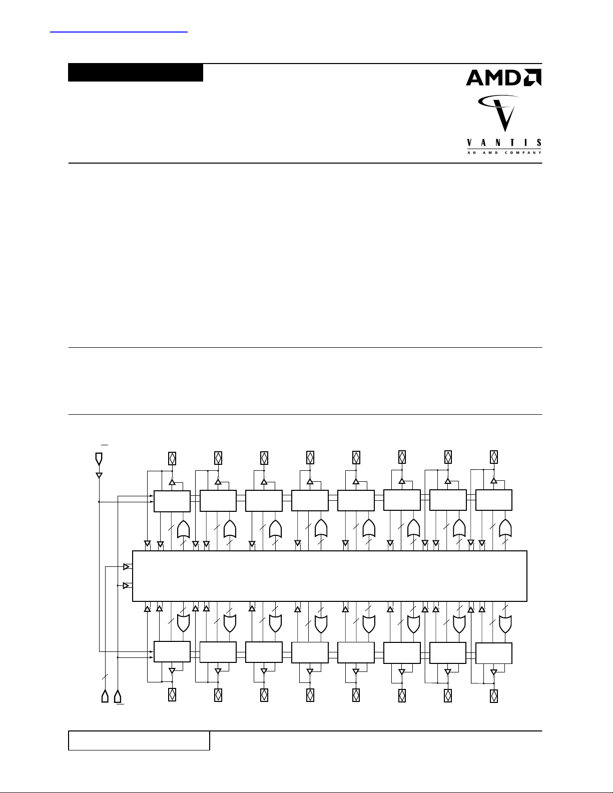
BLOCK DIAGRAM
I/OF
CLK/LE
4
I -I
I/OE
0 3
Publication# 08811 Rev. G Amendment/0
Issue Date: June 1993
7
I/O
Logic
V
Macrocell
4 4
4
4
I/O
V
Logic
Macrocell
I/OF
0
4
I/OF
Logic
V
Macrocell
V
Logic
Macrocell
I/OF
6
I/O
4
I/O
1
I/O
7
I/O
Logic
V
Macrocell
4
4
4
V
Logic
Macrocell
I/O
8
4
I/O
0
I/O
I/O
Logic
V
Macrocell
4
Programmable
AND Array
8
4
I/O
V
Logic
Macrocell
I/O
12
12
58x178
12
I/O
Logic
V
Macrocell
V
Logic
Macrocell
I/O
I/O
4
4
I/O
I/O
I/O
V
Logic
Macrocell
4
12
12
4
I/O
V
Logic
Macrocell
I/O
323
I/OF
5456
I/O
V
Logic
Macrocell
4
8
8
4
I/O
V
Logic
Macrocell
I/OF
I/OF
4
I/O
V
Logic
Macrocell
4
4
4
V
Logic
Macrocell
I/OF
4
4
4
I/O
08811G-1
2-349
Page 2
AMD
GENERAL DESCRIPTION (continued)
semicustom solutions such as gate arrays and standard
cells, including reduced development time and low upfront development cost.
The PALCE29MA16 uses the familiar sum-of-products
(AND-OR) structure, allowing users to customize logic
functions by programming the device for specific applications. It provides up to 29 array inputs and 16 outputs.
It incorporates AMD’s unique input/output logic macrocell which provides flexible input/output structure and
polarity, flexible feedback selection, multiple Output Enable choices, and a programmable clocking scheme.
The macrocells can be individually programmed as
combinatorial, registered, or latched with active-HIGH
or active-LOW polarity. The flexibility of the logic macrocells permits the system designer to tailor the device to
particular application requirements.
Increased logic power has been built into the
PALCE29MA16 by providing a varied number of logic
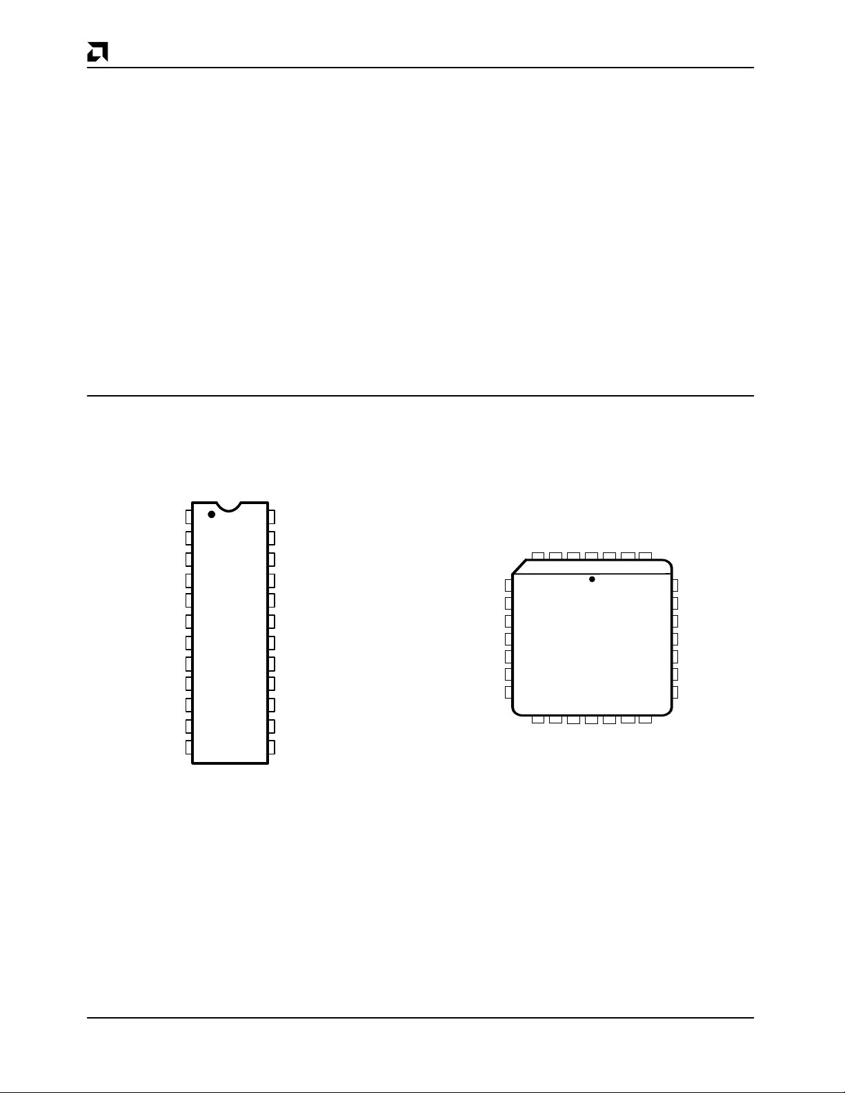
CONNECTION DIAGRAMS
Top View
SKINNYDIP
product terms per output. Of the 16 outputs, 8 outputs
have 4 product terms each, 4 outputs have 8 product
terms each, and the other 4 outputs have 12 product
terms each. This varied product-term distribution allows
complex functions to be implemented in a single PAL
device. Each output can be dynamically controlled by a
common Output Enable pin or Output Enable product
term. Each output can also be permanently enabled or
disabled.
System operation has been enhanced by the addition of
common asynchronous-Preset and Reset product
terms and a power-up Reset feature. The
PALCE29MA16 also incorporates Preload and Observability functions which permit full logic verification of
the design.
The PALCE29MA16 is offered in the space-saving
300-mil SKINNYDIP package as well as the plastic
leaded chip carrier package.
PLCC
Note:
CLK/LE
I/OF
I/OF
I/O
I/O
I/O
I/O
I/OF
I/OF
I/OE
GND
1
2
I
0
3
0
4
1
0
5
6
1
7
2
8
3
9
2
10
3
11
12
24
23
22
21
20
19
18
17
16
15
14
13
V
CC
I
3
I/OF
7
I/OF
6
I/O
7
I/O
6
I/O
5
I/O
4
I/OF
5
I/OF
4
I
2
I
1
08811G-2
Pin 1 is marked for orientation.
PIN DESIGNATIONS
CLK/LE = Clock or Latch Enable
GND = Ground
I = Input
I/O = Input/Output
I/OF = Input/Output with Dual Feedback
V
CC
NC = No Connection
= Supply Voltage
I/OF
I/O
I/O
NC
I/O
I/O
I/OF
7
CC
NC
I/OF0I0CLK/LE
5
1
6
0
7
1
8
9
2
10
3
11
2
12
131715 1614 18
3
I/OE
I/OF
V
I3I/OF
1324282726
I/OF
25
24
I/O
I/O
23
22
NC
I/O
21
I/O
20
I/OF
19
2
4
I1I
NC
GND
I/OF
08811G-3
6
7
6
5
4
5
2-350 PALCE29MA16H-25
Page 3
AMD
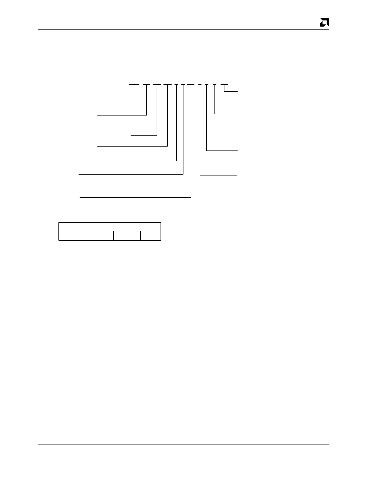
ORDERING INFORMATION
Commercial Products
AMD programmable logic products for commercial applications are available with several ordering options. The order number
(Valid Combination) is formed by a combination of these elements:
PAL CE 29 MA 16 H -25 C /4
FAMILY TYPE
PAL = Programmable Array Logic
TECHNOLOGY
CE = CMOS Electrically Erasable
NUMBER OF ARRAY INPUTS
OUTPUT TYPE
MA = Advanced Asynchronous Macrocell
NUMBER OF FLIP-FLOPS
POWER
H = Half Power (100 mA)
SPEED
-25 = 25 ns
Valid Combinations
PALCE29MA16H-25 PC, JC
/4
P
OPTIONAL PROCESSING
Blank = Standard Processing
PROGRAMMING REVISION
/4 = First Revision
(Requires current
programming Algorithm)
TEMPERATURE RANGE
C = Commercial (0
PACKAGE TYPE
P = 24-Pin Plastic SKINNYDIP
(PD3024)
J = 28-Pin Plastic Leaded Chip
Carrier (PL 028)
Valid Combinations
Valid Combinations lists configurations planned to
be supported in volume for this device. Consult the
local AMD sales office to confirm availability of
specific valid combinations and to check on newly
released combinations.
°C to +75°C)
2-351PALCE29MA16H-25 (Com’l)
Page 4
AMD
FUNCTIONAL DESCRIPTION
Inputs
The PALCE29MA16 has 29 inputs to drive each product
term (up to 58 inputs with both TRUE and complement
versions available to the AND array) as shown in the
block diagram in Figure 1. Of these 29 inputs, 4 are
dedicated inputs, 16 are from eight I/O logic macrocells
with two feedbacks, 8 are from other I/O logic macrocells with single feedback and one is the I/OE input.
Initially the AND-array gates are disconnected from all
the inputs. This condition represents a logical TRUE for
the AND array. By selectively programming the EE cells,
the AND array may be connected to either the TRUE input or the complement input. When both the TRUE and
complement inputs are connected, a logical FALSE results at the output of the AND gate.
Product Terms
The degree of programmability and complexity of a PAL
device is determined by the number of connections that
form the programmable-AND and OR gates. Each programmable-AND gate is called a product term. The
PALCE29MA16 has 178 product terms; 112 of these
product terms provide logic capability and others are architectural product terms. Among the control product
terms, one is for Observability, and one is for Preload.
The Output Enable of each macrocell can be programmed to be controlled by a common Output Enable
pin or an individual product term. It may also be permanently disabled. In addition, independent product terms
for each macrocell control Preset, Reset and CLK/LE.
Each product term on the PALCE29MA16 consists of a
58-input AND gate. The outputs of these AND gates are
connected to a fixed-OR plane. Product terms are allocated to OR gates in a varied distribution across the
device ranging from 4 to 12 wide, with an average of 7
logic product terms per output. An increased number of
product terms per output allows more complex functions
to be implemented in a single PAL device. This flexibility
aids in implementing functions such as counters, exclusive-OR functions, or complex state machines, where
different states require different numbers of product
terms.
Individual asynchronous-Preset and Reset product
terms are connected to all Registered or Latched I/Os.
When the asynchronous-Preset product term is asserted (HIGH) the register or latch will immediately be
loaded with a HIGH, independent of the clock. When the
asynchronous-Reset product term is asserted (HIGH)
the register or latch will be immediately loaded with a
LOW, independent of the clock. The actual output state
will depend on the macrocell polarity selection. The
latches must be in latched mode (not transparent mode)
for the Reset, Preset, Preload, and power-up Reset
modes to be meaningful.
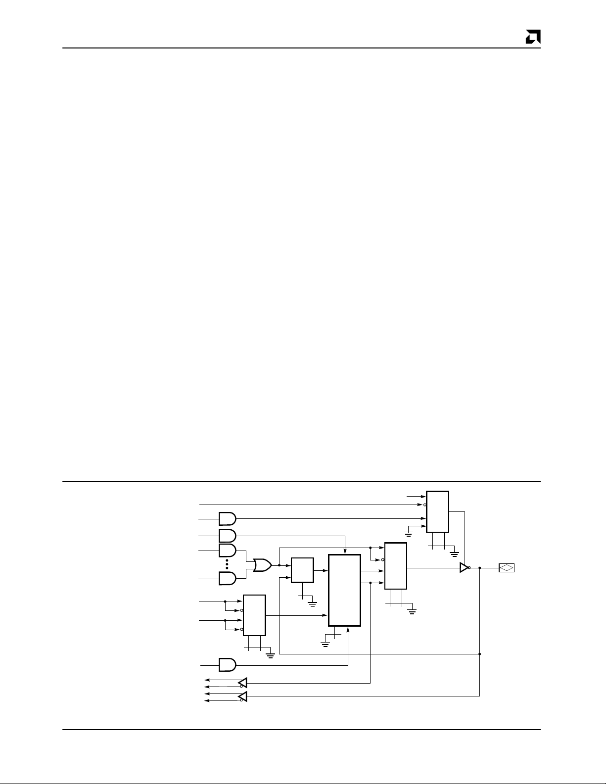
Input/Output Logic Macrocells
The I/O logic macrocell allows the user the flexibility of
defining the architecture of each input or output on an individual basis. It also provides the capability of using the
associated pin either as an input or an output.
The PALCE29MA16 has 16 macrocells, one for each
I/O pin. Each I/O macrocell can be programmed for
combinatorial, registered or latched operation (see Figure 2). Combinatorial output is desired when the PAL
device is used to replace combinatorial glue logic. Registers and Latches are used in synchronous logic
applications. Registers and Latches with product term
controlled clocks can also be used in asychronous
application.
Common I/OE (Pin)
Individual OE
Individual Asynchronous Preset
P0
P7 or P11
Common CLK/LE (PIN)
Individual CLK/LE
Individual Asynchronous Reset
To AND Array
S4
1
0
S3
1 1
1 0
0 1
0 0
S5
1
0
S8
S2
Preset
D
CLK/LE
V
Reset
Figure 2a. PALCE29MA16 Macrocell (Single Feedback)
2-352 PALCE29MA16H-25
V
CC
1 1
0 1
S0
R
1 0
0 0
X
Q
Q
S1
S6
0 1
1 1
1 0
0 0
S7
I/O
X
08811G-4
Page 5
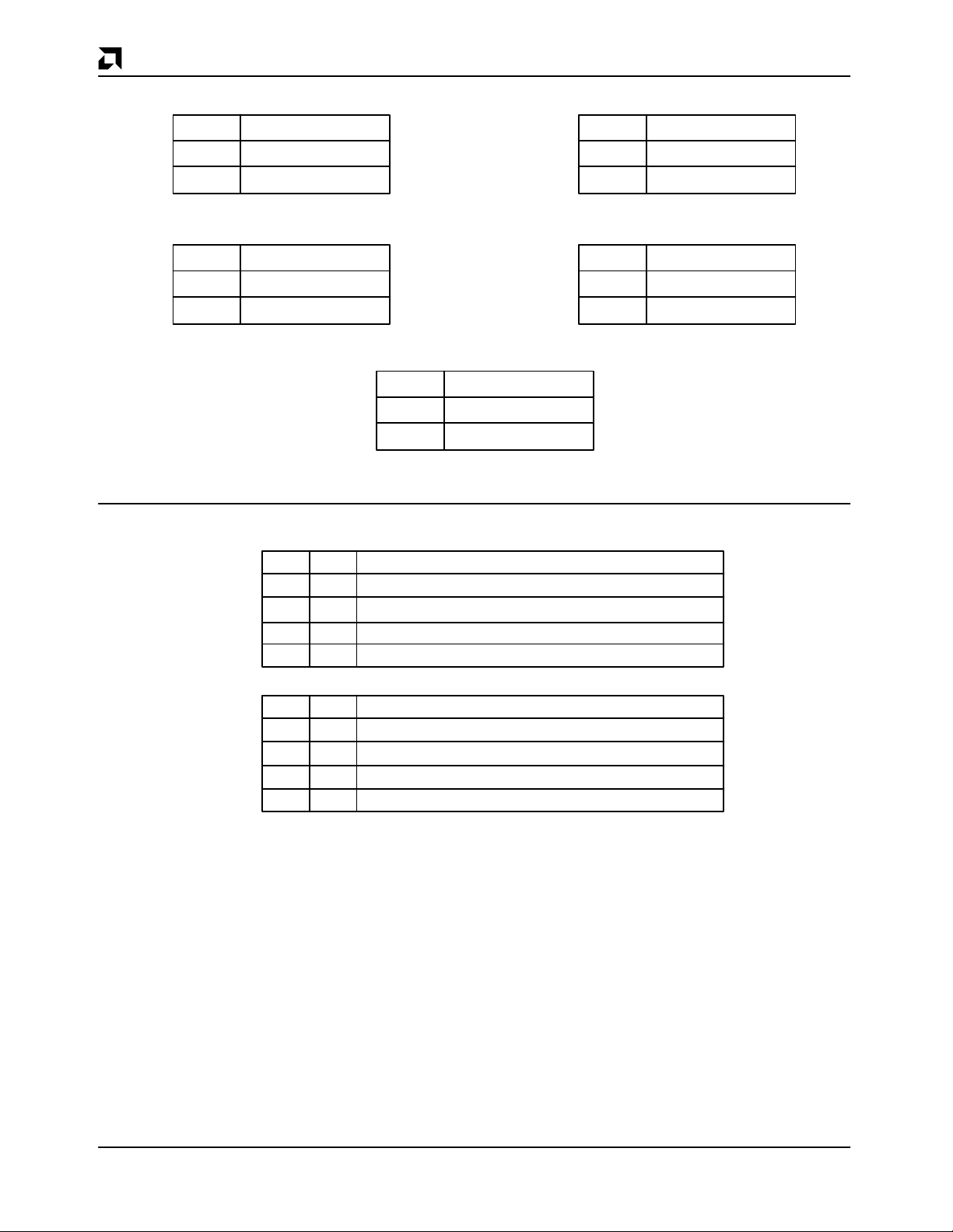
AMD
The output polarity for each macrocell in each of the
three modes of operation is user-selectable, allowing
complete flexibility of the macrocell configuration.
Eight of the macrocells (I/OF
–I/OF7) have two inde-
0
pendent feedback paths to the AND array (see Figure
2b). The first is a dedicated I/O pin feedback to the AND
array for combinatorial input. The second path consists
of a direct register/latch feedback to the array. If the pin
is used as a dedicated input using the first feedback
path, the register/latch feedback path is still available to
the AND array. This path provides the capability of using
the register/latch as a buried state register/latch. The
other eight macrocells have a single feedback path to
the AND array. This feedback is user-selectable as
either an I/O pin or a register/latch feedback (see
Figure2a).
Each macrocell can provide true input/output capability.
The user can select each macrocell register/latch to be
driven by either the signal generated by the AND-OR array or the corresponding I/O pin. When the I/O pin is selected as the input, the feedback path provides the
register/latch input to the array. When used as an input,
each macrocell is also user-programmable for registered, latched, or combinatorial input.
The PALCE29MA16 has a dedicated CLK/LE pin and
one individual CLK/LE product term or macrocell. All
macrocells have a programmable switch to choose between the CLK/LE pin and the CLK/LE product term as
the clock or latch enable signal. These signals are clock
signals for macrocells configured as registers and latch
enable signals for macrocells configured as latches.
The polarity of these CLK/LE signals is also individually
programmable. Thus different registers or latches can
be driven by different clocks and clock phases.
The Output-Enable mode of each of the macrocells can
be selected by the user. The I/O pin can be configured
as an output pin (permanently enabled) or as an input
pin (permanently disabled). It can also be configured as
a dynamic I/O controlled by the Output Enable pin or by
a product term.
I/O Logic Macrocell Configuration
AMD’s unique I/O macrocell offers major benefits
through its versatile, programmable input/output cell
structure, multiple clock choices, flexible Output Enable
and feedback selection. Eight I/O macrocells with single
feedback contain 9 EE
crocells contain 8 EE cells for programming the input/
output functions (see Table 1).
EE cell S
controls whether the macrocell will be combi-
1
natorial or registered/latched. S
larity (active-HIGH or active-LOW). S
whether the storage element is a register or a latch. S
allows the use of the macrocell as an input register/latch
or as an output register/latch. It selects the direction of
the data path through the register/latch. If connected to
the usual AND-OR array output, the register/latch is an
output connected to the I/O pin. If connected to the I/O
pin, the register/latch becomes an input register/latch to
the AND array using the feedback data path.
Programmable EE cells S
lect one of the four CLK/LE signals for each macrocell.
and S7 are used to control Output Enable as pin con-
S
6
trolled, product-term controlled, permanently enabled or
permanently disabled. S
plexer for the macrocells with a single feedback path
only.
Using the programmable EE cells S
and output configurations can be selected. Some of the
possible configuration options are shown in Figure 3.
In the erased state (charged, disconnected), an architectural cell is said to have a value of “1”; in the programmed state (discharged, connected to GND), an
architectural cell is said to have a value of “0.”
cells, while the other eight ma-
controls the output po-
0
determines
2
and S5 allow the user to se-
4
controls a feedback multi-
8
various input
0–S8
3
Common I/OE (Pin)
Individual OE
Individual Asynchronous Preset
P0
P3
Common CLK/LE (PIN)
Individual CLK/LE
Individual Asynchronous Reset
To AND Array
To AND Array
Figure 2b. PALCE29MA16 Macrocell (Dual Feedback)
S4
1 1
1 0
0 1
0 0
S5
S3
V
CC
1 1
S0
RF
0 1
1 0
0 0
X
S2
Preset
D
CLK/LE
V
Reset
Q
Q
1
0
S1
S6
0 1
1 1
1 0
0 0
S7
I/OF
08811G-5
X
2-353PALCE29MA16H-25
Page 6
AMD
Table 1a. PALCE29MA16 I/O Logic Macrocell Architecture Selections
S
3
I/O Cell
1 Output Cell
0 Input Cell
S
1
Output Type
1 Combinatorial
0 Register/Latch
S
8
Feedback*
S
2
Storage Element
1 Register
0 Latch
S
0
Output Polarity
1 Active LOW
0 Active HIGH
1 Register/Latch
0 I/O
*Applies to macrocells with single feedback only.
Table 1b. PALCE29MA16 I/O Logic Macrocell Clock Polarity and Output Enable Selections
S
S5Clock Edge/Latch Enable Level
4
1 1 CLK/LE pin positive-going edge, active-LOW LE*
1 0 CLK/LE pin negative-going edge, active-HIGH LE*
0 1 CLK/LE PT positive-going edge, active-LOW LE*
0 0 CLK/LE PT negative-going edge, active-HIGH LE*
S
S7Output Buffer Control
6
1 1 Pin-Controlled Three-State Enable
1 0 PT-Controlled Three-State Enable
0 1 Permanently Enabled (Output only)
0 0 Permanently Disabled (Input only)
Notes:
1 = Erased State (Charged or disconnected).
0 = Programmed State (Discharged or connected).
*Active-LOW LE means that data is stored when the
LE
is transparent when the
pin is LOW. Active-HIGH LE means the opposite.
LE
pin is HIGH, and the latch
2-354 PALCE29MA16H-25
Page 7
AMD
SOME POSSIBLE CONFIGURATIONS OF THE INPUT/OUTPUT LOGIC MACROCELL
(For other useful configurations, please refer to the macrocell diagrams in Figure 2. All macrocell architecture cells are
independently programmable).
DQ
Q
V
08811G-6
Output Registered/Active Low
S = 1
0
S = 0
1
S = 1
3
S = 1
2
Output Combinatorial/Active Low
DQ
Q
V
S = 1
0
S = 1
1
S = 1
3
08811G-7
DQ
Q
V
S = 0
0
S = 0
1
S = 1
3
S = 1
2
08811G-8
Output Registered/Active High
Figure 3a. Dual Feedback Macrocells
DQ
V
Q
S = 1
0
S = 0
1
S = 1
3
S = 0
8
S = 1
2
08811G-10
Output Registered/Active Low, I/O Feedback
DQ
Q
V
S = 0
0
S = 1
1
S = 1
3
08811G-9
Output Combinatorial/Active High
S = 1
0
S = 1
1
S = 1
3
S = 0
8
08811G-11
Output Combinatorial/Active Low, I/O Feedback
DQ
LE
Q
S = 0
0
S = 0
1
S = 1
3
S = 0
8
S = 0
2
08811G-12
Output Latched/Active High, I/O Feedback
Figure 3b. Single Feedback Macrocells
S = 0
0
S = 1
1
S = 1
3
S = 0
8
08811G-13
Output Combinatorial/Active High, I/O Feedback
2-355PALCE29MA16H-25
Page 8
AMD
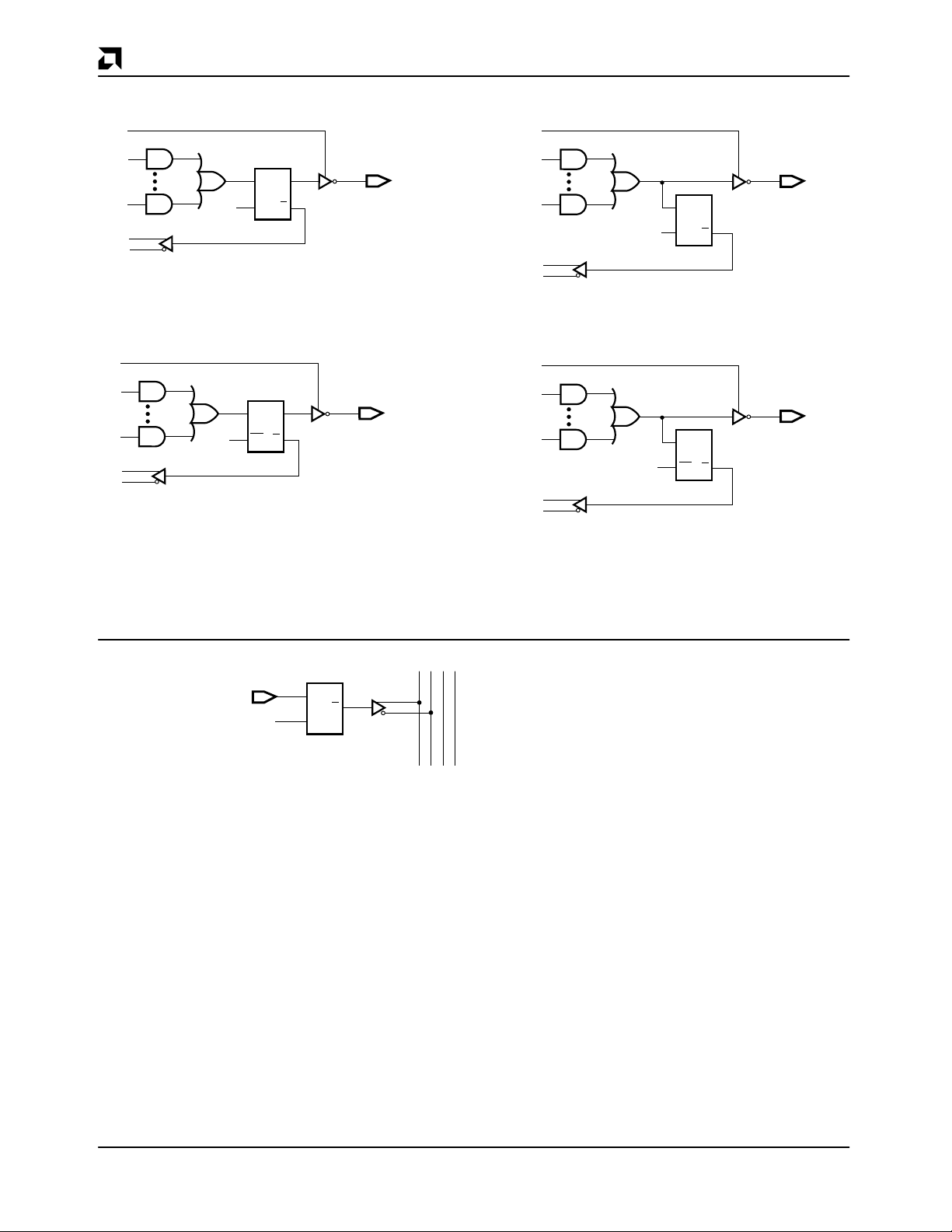
SOME POSSIBLE CONFIGURATIONS OF THE INPUT/OUTPUT LOGIC MACROCELL
DQ
Q
V
S = 1
S = 0
S = 1
S = 1
S = 1
08811G-14
Output Registered/Active Low,
Register Feedback
DQ
LE
Q
S = 1
0
S = 0
1
S = 1
3
S = 1
8
S = 0
2
08811G-16
Output Latched/Active Low,
Latched Feedback
0
1
3
8
2
DQ
V
Q
Output Combinatorial/Active Low,
Latched Feedback
DQ
LE
Q
Output Combinatorial/Active Low,
Latched Feedback
S = 1
0
S = 1
1
S = 1
3
S = 1
8
S = 1
2
08811G-15
S = 1
0
S = 1
1
S = 1
3
S = 1
8
S = 0
2
08811G-17
Figure 3b. Single Feedback Macrocells (Continued)
D
Q
V
PROGRAMMABLE-AND ARRAY
S = 0
3
S = 1 (FOR SINGLE FEEDBACK ONLY)
8
S = 1 REGISTER
2
= 0 LATCH
Programmable-AND Array
Figure 3c. All Macrocells
08811G-18
2-356 PALCE29MA16H-25
Page 9

AMD
Power-Up Reset
All flip-flops power up to a logic LOW for predictable system initialization. The outputs of the PALCE29MA16
depend on whether they are selected as registered or
combinatorial. If registered is selected, the output will be
LOW if programmed as active LOW and HIGH if programmed as active HIGH. If combinatorial is selected,
the output will be a function of the logic.
Preload
To simplify testing, the PALCE29MA16 is designed with
preload circuitry that provides an easy method for testing logical functionality. Both product-term-controlled
and supervoltage-enabled preload modes are
available. The TTL-level preload product term can be
useful during debugging, where supervoltages may not
be available.
Preload allows any arbitrary state value to be loaded
into the registers/latches of the device. A typical functional-test sequence would be to verify all possible state
transitions for the device being tested. This requires the
ability to set the state registers into an arbitrary “present
state” value and to set the device’s inputs into an arbitrary “present input” value. Once this is done, the state
machine is clocked into a new state, or “next state,”
which can be checked to validate the transition from the
“present state.” In this way any transition can be
checked.
Since preload can provide the capability to go directly to
any desired arbitrary state, test sequences may be
greatly shortened. Also, all possible states can be
tested, thus greatly reducing test time and development
costs and guaranteeing proper in-system operation.
Observability
The output register/latch observability product term,
when asserted, suppresses the combinatorial output
data from appearing on the I/O pin and allows the observation of the contents of the register/latch on the output
pin for each of the logic macrocells. This unique feature
allows for easy debugging and tracing of the buried state
machines. In addition, a capability of supervoltage observability is also provided.
Security Cell
A security cell is provided on each device to prevent unauthorized copying of the user’s proprietary logic design. Once programmed, the security cell disables the
programming, verification, preload, and the observability modes. The only way to erase the protection cell
is by erasing the entire array and architecture cells, in
which case no proprietary design can be copied. (This
cell should be programmed only after the rest of the device has been completely programmed and verified.)
Programming and Erasing
The PALCE29MA16 can be programmed on standard
logic programmers. It may also be erased to reset a previously configured device back to its virgin state.
Erasure is automatically performed by the programming
hardware. No special erasure operation is required.
Quality and Testability
The PALCE29MA16 offers a very high level of built-in
quality. The erasability of the device provides a direct
means of verifying performance of all the AC and DC parameters. In addition, this verifies complete programmability and functionality of the device to yield the
highest programming yield and post-programming functional yield in the industry.
Technology
The high-speed PALCE29MA16 is fabricated with
AMD’s advanced electrically-erasable (EE) CMOS
process. The array connections are formed with proven
EE cells. Inputs and outputs are designed to be compatible with TTL devices. This technology provides strong
input-clamp diodes, output slew-rate control, and a
grounded substrate for clean switching.
2-357PALCE29MA16H-25
Page 10

AMD
LOGIC DIAGRAM
SKINNY DIP (PLCC) Pinouts
CLK/LE
(2) 1
(3) 2
I
0
(4) 3
I/OF
(5) 4
I/OF
(6) 5
I/O
0
0
1
OBSERVE
PRODUCT
TERM
Input/
Output
Macro
Input/
Output
Macro
Input/
Output
Macro
0
48
12 16
20 24
28 32
36 40
44
48 52
56
23 (27)
I
3
22 (26)
I/OF
21 (25)
I/OF
7
6
Input/
Output
Macro
Input/
Output
Macro
(7) 6
I/O
1
Input/
Output
Macro
Continued on Next Page
2-358 PALCE29MA16H-25
Input/
Output
Macro
Input/
Output
Macro
08811G-19
20 (24)
I/O
19 (23)
I/O
6
7
Page 11

LOGIC DIAGRAM
SKINNY DIP (PLCC) Pinouts
048
(9) 7
I/O
(10) 8
I/O
2
3
Input/
Output
Macro
Input/
Output
Macro
12 16
Continued from Previous Page
20 24
28 32
36
40 44
AMD
52 56
48
18 (21)
I/O
Input/
Output
Macro
5
(11) 9
I/OF
(12) 10
I/OF
(13) 11
2
3
I/OE
PRELOAD
PRODUCT
TERM
Input/
Output
Macro
Input/
Output
Macro
Input/
Output
Macro
Input/
Output
Macro
Input/
Output
Macro
17 (20)
I/O
16 (19)
I/OF
15 (18)
I/OF
4
5
4
048
12 16
20 24
28 32
14 (17)
I
2
13 (16)
I
40 44
36
52 56
48
08811G-19
1
(concluded)
2-359PALCE29MA16H-25
Page 12

AMD
ABSOLUTE MAXIMUM RATINGS
Storage Temperature –65°C to +150°C. . . . . . . . . . .
Ambient Temperature
with Power Applied –55°C to +125°C. . . . . . . . . . . . .
Supply Voltage with
Respect to Ground –0.5 V to +7.0 V. . . . . . . . . . . . .
DC Input Voltage –0.5 V to V
DC Output or I/O
Pin Voltage –0.5 V to V
CC
CC
+ 0.5 V. . . . . . . . . . .
+ 0.5 V. . . . . . . . . . . . . . .
OPERATING RANGES
Commercial (C) Devices
Ambient Temperature (T
Operating in Free Air 0°C to +75°C. . . . . . . . . . . . . .
Supply Voltage (V
CC
with Respect to Ground +4.75 V to +5.25 V. . . . . . . .
Operating ranges define those limits between which the functionality of the device is guaranteed.
)
A
)
Static Discharge Voltage 2001 V. . . . . . . . . . . . . . . . .
Latchup Current (T
Stresses above those listed under Absolute Maximum Ratings may cause permanent device failure. Functionality at or
above these limits is not implied. Exposure to Absolute Maximum Ratings for extended periods may affect device reliability. Programming conditions may differ.
= 0°C to +75°C) 100 mA. . . . . .
A
DC CHARACTERISTICS over COMMERCIAL operating ranges unless otherwise
specified
Parameter
Symbol Parameter Description Test Conditions Min Max Unit
V
OH
V
OL
V
IH
V
IL
I
IH
I
IL
I
OZH
I
OZL
I
SC
I
CC
Notes:
1. These are absolute values with respect to device ground all overshoots due to system and/or tester noise are included.
2. I/O pin leakage is the worst case of I
3. Not more than one output should be shorted at a time and duration of the short-circuit should not exceed one second.
V
OUT
= 0.5 V has been chosen to avoid test problems caused by tester ground degradation.
Output HIGH Voltage IOH = –2 mA VIN = V
V
Output LOW Voltage IOL = 8 mA V
= 4 mA VCC = Min 0.33 V
I
OL
= 20 µA 0.1
I
OL
CC
IN
= V
IH
= Min
IH
or V
or V
IL
IL
2.4 V
0.5
Input HIGH Voltage Guaranteed Input Logical HIGH 2.0 V
Voltage for all Inputs (Note 1)
Input LOW Voltage Guaranteed Input Logical LOW 0.8 V
Voltage for all Inputs (Note 1)
Input HIGH Leakage Current VIN = 5.5 V, V
Input LOW Leakage Current V
Off-State Output Leakage V
Current HIGH V
Off-State Output Leakage V
Current LOW V
Output Short-Circuit Current V
= 0 V, V
IN
= 5.5 V, V
OUT
= V
IN
IH
= 5.5 V, V
OUT
= V
IN
IH
= 0.5 V, VCC = Max (Note 3) –30 –130 mA
OUT
Supply Current VIN = 0 V, Outputs Open (I
= Max
V
CC
IL
and I
OZL
(or IIH and I
OZH
= Max (Note 2) 10 µA
CC
= Max (Note 2) –10 µA
CC
= Max 10 µA
CC
or VIL (Note 2)
= Max –10 µA
CC
or VIL (Note 2)
= 0 mA) 100 mA
OUT
).
2-360 PALCE29MA16H-25 (Com’l)
Page 13

AMD
CAPACITANCE (Note 1)
Parameter
Symbol Parameter Description Test Conditions Typ Unit
C
C
OUT
IN
Input Capacitance V
Output Capacitance V
= 0 V VCC = 5.0 V, TA = 25°C, 5 pF
IN
= 0 V f = 1 MHz 8 pF
OUT
Note:
1. These parameters are not 100% tested, but are evaluated at initial characterization and at any time the design is modified
where capacitance may be affected.
SWITCHING CHARACTERISTICS
Registered Operation
Parameter
Symbol Parameter Description Min Max Unit
Combinatorial Output
t
PD
Output Register – Pin Clock
t
SOR
t
COR
t
HOR
Output Register – Product Term Clock
t
SORP
t
CORP
t
HORP
Input Register – Pin Clock
t
SIR
t
CIR
t
HIR
Clock and Frequency
t
CIS
t
CISPP
f
MAX
f
MAXI
f
MAXP
f
MAXIPP
t
CWH
t
CWL
t
CWHP
t
CWLP
Input or I/O Pin to Combinatorial Output 25 ns
Input or I/O Pin to Output Register Setup 15 ns
Output Register Clock to Output 15 ns
Data Hold Time for Output Register 0 ns
I/O Pin or Input to Output Register Setup 4 ns
Output Register Clock to Output 29 ns
Data Hold Time for Output Register 10 ns
I/O Pin to Input Register Setup 2 ns
Register Feedback Clock to Combinatorial Output 28 ns
Data Hold time for Input Register 6 ns
Register Feedback (Pin Driven Clock) to Output 20 ns
Register/Latch (Pin Driven) Setup
Register Feedback (PT Driven Clock) to Output 25 ns
Register/Latch (PT Driven) Setup
Maximum Frequency (Pin Driven) 1/(t
Maximum Internal Frequency (Pin Driven) 1/t
Maximum Frequency (PT Driven) 1/(t
Maximum Internal Frequency (PT Driven) 1/t
SOR
SORP
+ t
) 33.3 MHz
COR
50 MHz
40 MHz
+ t
CIS
) 30 MHz
CORP
CISPP
Pin Clock Width HIGH 8 ns
Pin Clock Width LOW 8 ns
PT Clock Width HIGH 12 ns
PT Clock Width LOW 12 ns
2-361PALCE29MA16H-25 (Com’l)
Page 14

AMD
CLK
t
SIR
Input
Register
AND-OR
t
CIS
V
V
Array
t
CIS
Output
Register
V
t
COR
I/O
I/O
t
SOR
t
PD
Input/Output Register Specs (Pin CLK Reference)
CLK
Input
AND-OR
Array
t
CISPP
Output
Register
V
I/O
V
V
Input
Register
t
CISPP
I/O
I/O
t
CIR
t
PD
08811G-20
t
CORP
I/O
I/O
t
SORP
t
PD
Input/Output Register Specs (PT CLK Reference)
2-362 PALCE29MA16H-25
I/O
t
PD
08811G-21
Page 15

SWITCHING WAVEFORMS
AMD
Combinatorial
Combinatorial
Combinatorial
Input
Output
Input
Clock
Registered
Output
V
T
t
PD
Combinatorial Output
Combinatorial Output
HOR
T
t
V
COR
V
T
t
SOR
t
V
Output Register (Pin Clock)
Output Register (Pin Clock)
V
T
T
V
08811G-22
T
08811G-23
Combinatorial
Combinatorial
Input as Clock
Input
Registered
Output
Registered
Input
Clock
Combinatorial
Output
t
CORP
HIR
t
CIR
V
T
t
V
T
V
T
t
SORP
V
T
Output Register (PT Clock)
Output Register (PT Clock)
V
T
t
SIR
Input Register
Input Register
t
V
T
HORP
V
T
V
T
08811G-24
08811G-25
2-363PALCE29MA16H-25
Page 16

AMD
SWITCHING WAVEFORMS
Clock
t
CIS
V
T
t
CWH
V
T
t
CWL
V
T
Combinatorial
Input as Clock
Pin Clock Width
Pin Clock Width
t
CISPP
V
T
t
CWLP
PT Clock Width
PT Clock Width
V
T
t
CWHP
08811G-26
V
T
08811G-27
2-364 PALCE29MA16H-25
Page 17

AMD
SWITCHING CHARACTERISTICS
Latched Operation
Parameter
Symbol Parameter Description Min Max Unit
Combinatorial Output
t
PD
t
PTD
Output Latch – Pin LE
t
SOL
t
GOL
t
HOL
t
STL
Output Latch – Product Term LE
t
SOLP
t
GOLP
t
HOLP
t
STLP
Input Latch – Pin LE
t
SIL
t
GIL
t
HIL
Input or I/O Pin to Combinatorial Output 25 ns
Input or I/O Pin to Output via Transparent Latch 28 ns
Input or I/O Pin to Output Register Setup 15 ns
Latch Enable to Transparent Mode Output 15 ns
Data Hold Time for Output Latch 0 ns
Input or I/O Pin to Output Latch Setup via 18 ns
Transparent Input Latch
Input or I/O Pin to Output Latch Setup 4 ns
Latch Enable to Transparent Mode Output 29 ns
Data Hold Time for Output Latch 10 ns
Input or I/O Pin to Output Latch Setup via 10 ns
Transparent Input Latch
I/O Pin to Input Latch Setup 2 ns
Latch Feedback, Latch Enable Transparent Mode to 28 ns
Combinatorial Output
Data Hold Time for Input Latch 6 ns
Latch Enable
t
GIS
t
GISPP
t
GWH
t
GWL
t
GWHP
t
GWLP
Latch Feedback (Pin Driven) to Output Register/Latch 20 ns
(Pin Driven) Setup
Latch Feedback (PT Driven) to Output Register/Latch 25 ns
(PT Driven) Setup
Pin Enable Width HIGH 8 ns
Pin Enable Width LOW 8 ns
PT Enable Width HIGH 12 ns
PT Enable Width LOW 12 ns
2-365PALCE29MA16H-25 (Com’l)
Page 18

AMD
LE
t
t
t
PTD
STL
SIL
Input
Latch
t
GIS
AND-OR
Array
t
GIS
Output
Latch
t
GOL
t
PTD
I/O
I/O
t
SOL
t
PTD
t
PD
Input/Output Latch Specs (Pin LE Reference)
LE
INPUT
AND-OR
t
STLP
t
PTD
I/O
Input
Latch
t
GISPP
Array
t
GISPP
Output
Latch
I/O
I/O
t
GIL
t
PTD
t
PD
08811G-28
t
GOLP
t
PTD
I/O
I/O
t
SOLP
t
PTD
t
PD
Input/Output Latch Specs (PT LE Reference)
2-366 PALCE29MA16H-25
I/O
t
PTD
t
PD
08811G-29
Page 19

SWITCHING WAVEFORMS
AMD
Latched
Input
Combinatorial
Combinatorial
Input
Output
Latched
Output
Latched
Input
Combinatorial
Input
Latched
Output
LE
V
T
t
PTD
V
T
t
PD
t
PTD
Latch (Transparent Mode)
V
T
t
STL
HOL
V
T
V
T
V
T
t
PTD
V
T
t
SOL
t
PTD
t
V
T
Output Latch (Pin LE)
V
T
V
T
08811G-30
Transparent
V
Note 1
08811G-32
t
GOL
T
LE
LE
Latched Transparent
V
T
t
GIS
Transparent
Input and Output Latch Relationship
Latched
Input
Combinatorial
Input
Combinatorial
Input as LE
Latched
Output
t
SOLP
V
T
t
STLP
V
T
V
t
PTD
Output Latch (PT LE)
Input
Latch
Output
Latched
V
T
Latch
08811G-31
t
HOLP
V
T
V
T
Transparent
T
t
GOLP
V
T
08811G-33
Latched
Input
LE
Combinatorial
Output
V
T
t
SIL
t
PTD
t
V
T
HIL
V
T
t
GIL
V
Transparent
T
V
T
V
T
LE
08811G-34
Input Latch (Pin LE)
Combinatorial
Input as LE
Note:
1. If the combinatorial input changes while
has elasped, the corresponding latched output will change t
binatorial input changes while
LE
elapsed, the corresponding latched output will change at the later of the following – t
input changes or t
ns after LE goes into the latched mode.
GOL
LE
is in the latched mode and LE goes into the transparent mode after t
ns after LE goes into the transparent mode. If the com-
GOL
is in the latched mode and LE goes into the transparent mode before t
TRANSPARENTLATCHED
V
T
t
GWH
V
T
t
GWL
Pin LE Width
Latched Transparent
V
T
t
GWLP
V
T
t
GWHP
PT LE Width
PTD
PTD
ns after the combinatorial
08811G-35
PTD
ns
ns has
V
T
V
T
08811G-36
2-367PALCE29MA16H-25
Page 20

AMD
SWITCHING CHARACTERISTICS
Reset/Preset, Enable
Parameter
Symbol Parameter Description Min Max Unit
t
APO
t
AW
t
ARO
t
ARI
t
ARPO
t
ARPI
Output Enable Operation
t
PZX
t
PXZ
t
EA
t
ER
Note:
1. Output disable times do not include test load RC time constants.
Input or I/O Pin to Output Register/Latch 30 ns
Reset/Preset
Asynchronous Reset/Preset Pulse Width 15 ns
Asynchronous Reset/Preset to Output 15 ns
Register/Latch Recovery
Asynchronous Reset/Preset to Input 12 ns
Register/Latch Recovery
Asynchronous Reset/Preset to Output 4 ns
Register/Latch Recovery PT Clock/LE
Asynchronous Reset/Preset to Input 6 ns
Register/Latch Recovery PT Clock/LE
I/OE Pin to Output Enable 20 ns
I/OE Pin to Output Disable (Note 1) 20 ns
Input or I/O to Output Enable via PT 25 ns
Input or I/O to Output Disable via PT (Note 1) 25 ns
SWITCHING WAVEFORMS
Combinatorial
Asynchronous
Reset/Preset
Registered/
Latched
Output
Clock
Output Register/Latch Reset/Preset
Combinatorial
Asynchronous
Reset/Preset
Clock
V
T
V
T
Input Register/Latch Reset/Preset
t
APO
t
AW
t
AW
V
t
ARO
T
Combinatorial/
V
T
08811G-37
Pin 11
Registered/
Latched
Output
t
PXZ
V
T
V
OH
VOL+ 0.5 V
- 0.5 V
t
PZX
V
08811G-39
T
Pin 11 to Output Disable/Enable
t
ARI
08811G-38
Combinatorial
Input
t
ER
V
OH
VOL+ 0.5 V
T
Combinatorial/
Registered/
V
Latched
Output
- 0.5 V
V
T
t
EA
V
T
08811G-40
Input to Output Disable/Enable
2-368 PALCE29MA16H-25 (Com’l)
Page 21

KEY TO SWITCHING WAVEFORMS
WAVEFORM INPUTS OUTPUTS
AMD
SWITCHING TEST CIRCUIT
5 V
Must be
Steady
May
Change
from H to L
May
Change
from L to H
Don’t Care,
Any Change
Permitted
Does Not
Apply
S
1
Will be
Steady
Will be
Changing
from H to L
Will be
Changing
from L to H
Changing,
State
Unknown
Center
Line is HighImpedance
“Off” State
KS000010-PAL
Specification Switch S
t
PD
t
EA
, tCO, t
, t
PZX
GOL
Closed 1.5 V
Z→H: open 1.5 V
Z→L: closed
, t
t
ER
PXZ
H→Z: open 5 pF H→Z: VOH –0.5 V
L→Z: closed L→Z: V
Output
1
C
C
L
35 pF
R
1
R
R
2
2
08811G-41
Measured Output Value
+0.5 V
OL
L
R
1
470 Ω
390 Ω
2-369PALCE29MA16H-25
Page 22

AMD
PRELOAD
The PALCE29MA16 has the capability for product-term
Preload. When the global-preload product term is true,
the PALCE29MA16 will enter the preload mode. This
feature aids functional testing by allowing direct setting
of register states. The procedure for Preload is as
follows:
■ Set the selected input pins to the user selected
preload condition.
■ Apply the desired register value to the I/O pins.
This sets Q of the register. The value seen on the
I/O pin, after Preload, will depend on whether the
macrocell is active high or active low.
Parameter
Symbol Parameter Description Min Rec. Max Unit
t
D
t
W
t
I/O
Delay Time 0.5 1.0 5.0 µs
Pulse Width 250 500 700 ns
Valid Output 100 500 ns
■ Pulse the clock pin (pin 1).
■ Remove the inputs to the I/O pins.
■ Remove the Preload condition.
■ Verify V
for all output pins as per pro-
OL/VOH
grammed pattern.
Because the Preload command is a product term, any
input to the array can be used to set Preload (including
I/O pins and registers). Preload itself will change the values of the I/O pins and registers. This will have unpredictable results. Therefore, only dedicated input pins
should be used for the Preload command.
Inputs
I/O Pins
CLK
Pin 1 (2)
V
Preload Mode
t
D
Data to be
Preloaded
t
D
t
W
t
D
t
IO
IH
V
IL
VOH/V
VOL/V
V
IH
V
IL
08811G-42
IH
IL
Preload Waveform
2-370 PALCE29MA16H-25
Page 23

AMD
OBSERVABILITY
The PALCE29MA16 has the capability for product-term
Observability. When the global-Observe product term is
true, the PALCE29MA16 will enter the Observe mode.
This feature aids functional testing by allowing direct observation of register states.
When the PALCE29MA16 is in the Observe mode, the
output buffer is enabled and the I/O pin value will be Q of
the corresponding register. This overrides any OE
inputs.
The procedure for Observe is:
■ Remove the inputs to all the I/O pins.
Parameter
Symbol Parameter Description Min Rec. Max Unit
t
D
t
I/O
Input
Pins
I/O Pins
Delay Time 0.5 1.0 5.0 µs
Valid Output 100 500 ns
Observe Mode
t
D
■ Set the inputs to the, user selected, Observe
configuration.
■ The register values will be sent to the correspond-
ing I/O pins.
■ Remove the Observe configuration from the se-
lected I/O pins.
Because the Observe command is a product term, any
input to the array can be used to set Observe (including
I/O pins and registers). If I/O pins are used, the observe
mode could cause a value change, which would cause
the device to oscillate in and out of the Observe mode.
Therefore, only dedicated input pins should be used for
the Observe command.
V
IH
V
t
IO
IL
V
OH
V
OL
CLK
Pin 1 (2)
Observability Waveform
V
IH
V
IL
08811G-43
2-371PALCE29MA16H-25
Page 24

AMD
POWER-UP RESET
The registered devices in the AMD PAL Family have
been designed with the capability to reset during system
power-up. Following power-up, all registers will be reset
to LOW. The output state will depend on the polarity of
the output buffer. This feature provides extra flexibility
to the designer and is especially valuable in simplifying state machine initialization. A timing diagram and
parameter table are shown below. Due to the
Parameter
Symbol Parameter Description Min Max Unit
t
PR
t
S
t
W
t
R
Registered
Active LOW
Power-Up Reset Time 10 µs
Input or Feedback Setup Time
Clock Width
V
Rise Time 500 µs
CC
Power
Output
4 V
t
R
t
asynchronous operation of the power-up reset, and the
wide range of ways V
can rise to its steady state, two
CC
conditions are required to ensure a valid power-up reset. These conditions are:
■ The V
■ Following reset, the clock input must not be driven
rise must be monotonic.
CC
from LOW to HIGH until all applicable input and
feedback setup times are met.
See Switching Characteristics
PR
t
S
V
CC
Clock
t
W
Power-Up Reset Waveform
08811G-44
2-372 PALCE29MA16H-25
Page 25

AMD
TYPICAL THERMAL CHARACTERISTICS
Measured at 25°C ambient. These parameters are not tested.
Parameter
Symbol Parameter Description SKINNYDIP PLCC Unit
θ
jc
θ
ja
θ
jma
Thermal impedance, junction to case 17 11 °C/W
Thermal impedance, junction to ambient 63 51 °C/W
Thermal impedance, junction to ambient with air flow 200 lfpm air 60 43 °C/W
400 lfpm air 52 38 °C/W
600 lfpm air 43 34 °C/W
800 lfpm air 39 30 °C/W
Plastic θjc Considerations
θ
The data listed for plastic
heat-flow paths in plastic-encapsulated devices are complex, making the
jc are for reference only and are not recommended for use in calculating junction temperatures. The
θ
jc measurement relative to a specific location on the
package surface. Tests indicate this measurement reference point is directly below the die-attach area on the bottom center of the
θ
package. Furthermore,
jc tests on packages are performed in a constant-temperature bath, keeping the package surface at a
constant temperature. Therefore, the measurements can only be used in a similar environment.
Typ
2-373PALCE29MA16H-25
 Loading...