

Page 1

AMD Geode™ LX Processors
Data Book
February 2009
Publication ID: 33234H
AMD Geode™ LX Processors Data Book
Page 2

© 2009 Advanced Micro Devices, Inc. All rights reserved.
The contents of this document are provided in connection with Advanced Micro
Devices, Inc. (“AMD”) products. AMD makes no representations or warranties with
respect to the accuracy or completeness of the contents of this publication and
reserves the right to make changes to specifications and product descriptions at
any time without notice. No license, whether express, implied, arising by estoppel
or otherwise, to any intellectual property rights is granted by this publication.
Except as set forth in AMD’s Standard Terms and Conditions of Sale, AMD
assumes no liability whatsoever, and disclaims any express or implied warranty,
relating to its products including, but not limited to, the implied warranty of merchantability, fitness for a particular purpose, or infringement of any intellectual
property right.
AMD’s products are not designed, intended, authorized or warranted for use as
components in systems intended for surgical implant into the body, or in other
applications intended to support or sustain life, or in any other application in which
the failure of AMD’s product could create a situation where personal injury, death,
or severe property or environmental damage may occur. AMD reserves the right to
discontinue or make changes to its products at any time without notice.
Contacts
www.amd.com
Trademarks
AMD, the AMD Arrow logo, AMD Athlon, Geode, GeodeLink, 3DNow!, and combinations thereof, are trademarks of
Advanced Micro Devices, Inc.
Linux is a registered trademark of Linus Torvalds.
WinBench is a registered trademark of Ziff Davis, Inc.
Windows is a registered trademark of Microsoft Corporation in the United States and/or other jurisdictions.
Pentium is a registered trademark and MMX is a trademark of Intel Corporation in the United States and/or other jurisdictions.
Other product names used in this publication are for identification purposes only and may be trademarks of their respective
companies.
2 AMD Geode™ LX Processors Data Book
Page 3

Contents 33234H
Contents
List of Figures . . . . . . . . . . . . . . . . . . . . . . . . . . . . . . . . . . . . . . . . . . . . . . . . . . . . . . . . . . 5
List of Tables . . . . . . . . . . . . . . . . . . . . . . . . . . . . . . . . . . . . . . . . . . . . . . . . . . . . . . . . . . . 7
1.0 Overview . . . . . . . . . . . . . . . . . . . . . . . . . . . . . . . . . . . . . . . . . . . . . . . . . . . . . . . . . 11
1.1 General Description . . . . . . . . . . . . . . . . . . . . . . . . . . . . . . . . . . . . . . . . . . . . . . . . . . . . . . . . . . 11
1.2 Features . . . . . . . . . . . . . . . . . . . . . . . . . . . . . . . . . . . . . . . . . . . . . . . . . . . . . . . . . . . . . . . . . . . 12
2.0 Architecture Overview . . . . . . . . . . . . . . . . . . . . . . . . . . . . . . . . . . . . . . . . . . . . . . 15
2.1 CPU Core . . . . . . . . . . . . . . . . . . . . . . . . . . . . . . . . . . . . . . . . . . . . . . . . . . . . . . . . . . . . . . . . . 15
2.2 GeodeLink™ Control Processor . . . . . . . . . . . . . . . . . . . . . . . . . . . . . . . . . . . . . . . . . . . . . . . .16
2.3 GeodeLink™ Interface Units . . . . . . . . . . . . . . . . . . . . . . . . . . . . . . . . . . . . . . . . . . . . . . . . . . . 16
2.4 GeodeLink™ Memory Controller . . . . . . . . . . . . . . . . . . . . . . . . . . . . . . . . . . . . . . . . . . . . . . . . 16
2.5 Graphics Processor . . . . . . . . . . . . . . . . . . . . . . . . . . . . . . . . . . . . . . . . . . . . . . . . . . . . . . . . . . 17
2.6 Display Controller . . . . . . . . . . . . . . . . . . . . . . . . . . . . . . . . . . . . . . . . . . . . . . . . . . . . . . . . . . . . 18
2.7 Video Processor . . . . . . . . . . . . . . . . . . . . . . . . . . . . . . . . . . . . . . . . . . . . . . . . . . . . . . . . . . . . 18
2.8 Video Input Port . . . . . . . . . . . . . . . . . . . . . . . . . . . . . . . . . . . . . . . . . . . . . . . . . . . . . . . . . . . . . 18
2.9 GeodeLink™ PCI Bridge . . . . . . . . . . . . . . . . . . . . . . . . . . . . . . . . . . . . . . . . . . . . . . . . . . . . . . 18
2.10 Security Block . . . . . . . . . . . . . . . . . . . . . . . . . . . . . . . . . . . . . . . . . . . . . . . . . . . . . . . . . . . . . . 19
3.0 Signal Definitions . . . . . . . . . . . . . . . . . . . . . . . . . . . . . . . . . . . . . . . . . . . . . . . . . . 21
3.1 Buffer Types . . . . . . . . . . . . . . . . . . . . . . . . . . . . . . . . . . . . . . . . . . . . . . . . . . . . . . . . . . . . . . . . 23
3.2 Bootstrap Options . . . . . . . . . . . . . . . . . . . . . . . . . . . . . . . . . . . . . . . . . . . . . . . . . . . . . . . . . . . 24
3.3 Ball Assignments . . . . . . . . . . . . . . . . . . . . . . . . . . . . . . . . . . . . . . . . . . . . . . . . . . . . . . . . . . . . 24
3.4 Signal Descriptions . . . . . . . . . . . . . . . . . . . . . . . . . . . . . . . . . . . . . . . . . . . . . . . . . . . . . . . . . . 33
4.0 GeodeLink™ Interface Unit . . . . . . . . . . . . . . . . . . . . . . . . . . . . . . . . . . . . . . . . . . 45
4.1 MSR Set . . . . . . . . . . . . . . . . . . . . . . . . . . . . . . . . . . . . . . . . . . . . . . . . . . . . . . . . . . . . . . . . . . 45
4.2 GLIU Register Descriptions . . . . . . . . . . . . . . . . . . . . . . . . . . . . . . . . . . . . . . . . . . . . . . . . . . . . 50
5.0 CPU Core . . . . . . . . . . . . . . . . . . . . . . . . . . . . . . . . . . . . . . . . . . . . . . . . . . . . . . . . 89
5.1 Core Processor Initialization . . . . . . . . . . . . . . . . . . . . . . . . . . . . . . . . . . . . . . . . . . . . . . . . . . . 89
5.2 Instruction Set Overview . . . . . . . . . . . . . . . . . . . . . . . . . . . . . . . . . . . . . . . . . . . . . . . . . . . . . . 90
5.3 Application Register Set . . . . . . . . . . . . . . . . . . . . . . . . . . . . . . . . . . . . . . . . . . . . . . . . . . . . . . 91
5.4 System Register Set . . . . . . . . . . . . . . . . . . . . . . . . . . . . . . . . . . . . . . . . . . . . . . . . . . . . . . . . . 94
5.5 CPU Core Register Descriptions . . . . . . . . . . . . . . . . . . . . . . . . . . . . . . . . . . . . . . . . . . . . . . . .99
AMD Geode™ LX Processors Data Book 3
Page 4

33234H
Contents
6.0 Integrated Functions . . . . . . . . . . . . . . . . . . . . . . . . . . . . . . . . . . . . . . . . . . . . . . 209
6.1 GeodeLink™ Memory Controller . . . . . . . . . . . . . . . . . . . . . . . . . . . . . . . . . . . . . . . . . . . . . . . 210
6.2 GeodeLink™ Memory Controller Register Descriptions . . . . . . . . . . . . . . . . . . . . . . . . . . . . . 219
6.3 Graphics Processor . . . . . . . . . . . . . . . . . . . . . . . . . . . . . . . . . . . . . . . . . . . . . . . . . . . . . . . . . 237
6.4 Graphics Processor Register Definitions . . . . . . . . . . . . . . . . . . . . . . . . . . . . . . . . . . . . . . . . . 254
6.5 Display Controller . . . . . . . . . . . . . . . . . . . . . . . . . . . . . . . . . . . . . . . . . . . . . . . . . . . . . . . . . . . 278
6.6 Display Controller Register Descriptions . . . . . . . . . . . . . . . . . . . . . . . . . . . . . . . . . . . . . . . . . 300
6.7 Video Processor . . . . . . . . . . . . . . . . . . . . . . . . . . . . . . . . . . . . . . . . . . . . . . . . . . . . . . . . . . . 388
6.8 Video Processor Register Descriptions . . . . . . . . . . . . . . . . . . . . . . . . . . . . . . . . . . . . . . . . . . 412
6.9 Video Input Port . . . . . . . . . . . . . . . . . . . . . . . . . . . . . . . . . . . . . . . . . . . . . . . . . . . . . . . . . . . . 462
6.10 Video Input Port Register Descriptions . . . . . . . . . . . . . . . . . . . . . . . . . . . . . . . . . . . . . . . . . . 482
6.11 Security Block . . . . . . . . . . . . . . . . . . . . . . . . . . . . . . . . . . . . . . . . . . . . . . . . . . . . . . . . . . . . . 510
6.12 Security Block Register Descriptions . . . . . . . . . . . . . . . . . . . . . . . . . . . . . . . . . . . . . . . . . . . . 513
6.13 GeodeLink™ Control Processor . . . . . . . . . . . . . . . . . . . . . . . . . . . . . . . . . . . . . . . . . . . . . . . 533
6.14 GeodeLink™ Control Processor Register Descriptions . . . . . . . . . . . . . . . . . . . . . . . . . . . . . . 539
6.15 GeodeLink™ PCI Bridge . . . . . . . . . . . . . . . . . . . . . . . . . . . . . . . . . . . . . . . . . . . . . . . . . . . . . 566
6.16 GeodeLink™ PCI Bridge Register Descriptions . . . . . . . . . . . . . . . . . . . . . . . . . . . . . . . . . . . 572
7.0 Electrical Specifications . . . . . . . . . . . . . . . . . . . . . . . . . . . . . . . . . . . . . . . . . . . 597
7.1 Electrical Connections . . . . . . . . . . . . . . . . . . . . . . . . . . . . . . . . . . . . . . . . . . . . . . . . . . . . . . . 597
7.2 Absolute Maximum Ratings . . . . . . . . . . . . . . . . . . . . . . . . . . . . . . . . . . . . . . . . . . . . . . . . . . . 597
7.3 Operating Conditions . . . . . . . . . . . . . . . . . . . . . . . . . . . . . . . . . . . . . . . . . . . . . . . . . . . . . . . . 598
7.4 DC Current . . . . . . . . . . . . . . . . . . . . . . . . . . . . . . . . . . . . . . . . . . . . . . . . . . . . . . . . . . . . . . . . 599
7.5 DC Characteristics . . . . . . . . . . . . . . . . . . . . . . . . . . . . . . . . . . . . . . . . . . . . . . . . . . . . . . . . . . 604
7.6 AC Characteristics . . . . . . . . . . . . . . . . . . . . . . . . . . . . . . . . . . . . . . . . . . . . . . . . . . . . . . . . . . 607
8.0 Instruction Set . . . . . . . . . . . . . . . . . . . . . . . . . . . . . . . . . . . . . . . . . . . . . . . . . . . 619
8.1 General Instruction Set Format . . . . . . . . . . . . . . . . . . . . . . . . . . . . . . . . . . . . . . . . . . . . . . . . 619
8.2 CPUID Instruction Set . . . . . . . . . . . . . . . . . . . . . . . . . . . . . . . . . . . . . . . . . . . . . . . . . . . . . . . 627
8.3 Processor Core Instruction Set . . . . . . . . . . . . . . . . . . . . . . . . . . . . . . . . . . . . . . . . . . . . . . . . 633
8.4 MMX™, FPU, and AMD 3DNow!™ Technology Instructions Sets . . . . . . . . . . . . . . . . . . . . . . 658
9.0 Package Specifications . . . . . . . . . . . . . . . . . . . . . . . . . . . . . . . . . . . . . . . . . . . . 675
9.1 Physical Dimensions . . . . . . . . . . . . . . . . . . . . . . . . . . . . . . . . . . . . . . . . . . . . . . . . . . . . . . . . 675
Appendix A Support Documentation . . . . . . . . . . . . . . . . . . . . . . . . . . . . . . . . . . . . 677
A.1 Order Information . . . . . . . . . . . . . . . . . . . . . . . . . . . . . . . . . . . . . . . . . . . . . . . . . . . . . . . . . . 677
A.2 Data Book Revision History . . . . . . . . . . . . . . . . . . . . . . . . . . . . . . . . . . . . . . . . . . . . . . . . . . 679
4 AMD Geode™ LX Processors Data Book
Page 5

List of Figures 33234H
List of Figures
Figure 1-1. Internal Block Diagram . . . . . . . . . . . . . . . . . . . . . . . . . . . . . . . . . . . . . . . . . . . . . . . . . . . . . . 11
Figure 3-1. Signal Groups . . . . . . . . . . . . . . . . . . . . . . . . . . . . . . . . . . . . . . . . . . . . . . . . . . . . . . . . . . . . 21
Figure 3-2. BGU481 Ball Assignment Diagram . . . . . . . . . . . . . . . . . . . . . . . . . . . . . . . . . . . . . . . . . . . . 25
Figure 4-1. GeodeLink™ Architecture . . . . . . . . . . . . . . . . . . . . . . . . . . . . . . . . . . . . . . . . . . . . . . . . . . . 46
Figure 6-1. Integrated Functions Block Diagram . . . . . . . . . . . . . . . . . . . . . . . . . . . . . . . . . . . . . . . . . . 209
Figure 6-2. GLMC Block Diagram . . . . . . . . . . . . . . . . . . . . . . . . . . . . . . . . . . . . . . . . . . . . . . . . . . . . . 210
Figure 6-3. HOI Addressing Example . . . . . . . . . . . . . . . . . . . . . . . . . . . . . . . . . . . . . . . . . . . . . . . . . . . 211
Figure 6-4. HOI Example . . . . . . . . . . . . . . . . . . . . . . . . . . . . . . . . . . . . . . . . . . . . . . . . . . . . . . . . . . . . 211
Figure 6-5. LOI Addressing Example . . . . . . . . . . . . . . . . . . . . . . . . . . . . . . . . . . . . . . . . . . . . . . . . . . . 212
Figure 6-6. LOI Example . . . . . . . . . . . . . . . . . . . . . . . . . . . . . . . . . . . . . . . . . . . . . . . . . . . . . . . . . . . . 212
Figure 6-7. Request Pipeline . . . . . . . . . . . . . . . . . . . . . . . . . . . . . . . . . . . . . . . . . . . . . . . . . . . . . . . . . 215
Figure 6-8. DDR Reads . . . . . . . . . . . . . . . . . . . . . . . . . . . . . . . . . . . . . . . . . . . . . . . . . . . . . . . . . . . . . 216
Figure 6-9. DDR Writes . . . . . . . . . . . . . . . . . . . . . . . . . . . . . . . . . . . . . . . . . . . . . . . . . . . . . . . . . . . . . 217
Figure 6-10. Graphics Processor Block Diagram . . . . . . . . . . . . . . . . . . . . . . . . . . . . . . . . . . . . . . . . . . . 237
Figure 6-11. 14-Bit Repeated Pattern . . . . . . . . . . . . . . . . . . . . . . . . . . . . . . . . . . . . . . . . . . . . . . . . . . . 244
Figure 6-12. Display Controller High-Level Block Diagram . . . . . . . . . . . . . . . . . . . . . . . . . . . . . . . . . . . 278
Figure 6-13. GUI Block Diagram . . . . . . . . . . . . . . . . . . . . . . . . . . . . . . . . . . . . . . . . . . . . . . . . . . . . . . . 279
Figure 6-14. VGA Block Diagram . . . . . . . . . . . . . . . . . . . . . . . . . . . . . . . . . . . . . . . . . . . . . . . . . . . . . . . 280
Figure 6-15. VGA Frame Buffer Organization . . . . . . . . . . . . . . . . . . . . . . . . . . . . . . . . . . . . . . . . . . . . . 288
Figure 6-16. Graphics Controller High-level Diagram . . . . . . . . . . . . . . . . . . . . . . . . . . . . . . . . . . . . . . . 289
Figure 6-17. Write Mode Data Flow . . . . . . . . . . . . . . . . . . . . . . . . . . . . . . . . . . . . . . . . . . . . . . . . . . . . . 290
Figure 6-18. Read Mode Data Flow . . . . . . . . . . . . . . . . . . . . . . . . . . . . . . . . . . . . . . . . . . . . . . . . . . . . . 291
Figure 6-19. Color Compare Operation . . . . . . . . . . . . . . . . . . . . . . . . . . . . . . . . . . . . . . . . . . . . . . . . . . 292
Figure 6-20. Graphics Filter Block Diagram . . . . . . . . . . . . . . . . . . . . . . . . . . . . . . . . . . . . . . . . . . . . . . . 293
Figure 6-21. Flicker Filter and Line Buffer Path . . . . . . . . . . . . . . . . . . . . . . . . . . . . . . . . . . . . . . . . . . . . 295
Figure 6-22. Interlaced Timing Settings . . . . . . . . . . . . . . . . . . . . . . . . . . . . . . . . . . . . . . . . . . . . . . . . . . 298
Figure 6-23. Video Processor Block Diagram . . . . . . . . . . . . . . . . . . . . . . . . . . . . . . . . . . . . . . . . . . . . . 389
Figure 6-24. Video Processor Block Diagram . . . . . . . . . . . . . . . . . . . . . . . . . . . . . . . . . . . . . . . . . . . . . 390
Figure 6-25. Downscaler Block Diagram . . . . . . . . . . . . . . . . . . . . . . . . . . . . . . . . . . . . . . . . . . . . . . . . . 392
Figure 6-26. Linear Interpolation Calculation . . . . . . . . . . . . . . . . . . . . . . . . . . . . . . . . . . . . . . . . . . . . . . 393
Figure 6-27. Mixer Block Diagram . . . . . . . . . . . . . . . . . . . . . . . . . . . . . . . . . . . . . . . . . . . . . . . . . . . . . . 395
Figure 6-28. Color Key and Alpha-Blending Logic . . . . . . . . . . . . . . . . . . . . . . . . . . . . . . . . . . . . . . . . . . 396
Figure 6-29. VOP Internal Block Diagram . . . . . . . . . . . . . . . . . . . . . . . . . . . . . . . . . . . . . . . . . . . . . . . . 398
Figure 6-30. 525-Line NTSC Video Window . . . . . . . . . . . . . . . . . . . . . . . . . . . . . . . . . . . . . . . . . . . . . . 399
Figure 6-31. HBLANK and VBLANK for Lines 20-262, 283-524 . . . . . . . . . . . . . . . . . . . . . . . . . . . . . . . 399
Figure 6-32. HBLANK and VBLANK for Lines 263, 525 . . . . . . . . . . . . . . . . . . . . . . . . . . . . . . . . . . . . . . 400
Figure 6-33. HBLANK and VBLANK for Lines 1-18, 264-281 . . . . . . . . . . . . . . . . . . . . . . . . . . . . . . . . . 400
Figure 6-34. HBLANK and VBLANK for Lines 19, 282 . . . . . . . . . . . . . . . . . . . . . . . . . . . . . . . . . . . . . . . 400
Figure 6-35. BT.656 8/16 Bit Line Data . . . . . . . . . . . . . . . . . . . . . . . . . . . . . . . . . . . . . . . . . . . . . . . . . . 403
Figure 6-36. Flat Panel Display Controller Block Diagram . . . . . . . . . . . . . . . . . . . . . . . . . . . . . . . . . . . . 405
Figure 6-37. Dithered 8x8 Pixel Pattern . . . . . . . . . . . . . . . . . . . . . . . . . . . . . . . . . . . . . . . . . . . . . . . . . . 408
Figure 6-38. N-Bit Dithering Pattern Schemes . . . . . . . . . . . . . . . . . . . . . . . . . . . . . . . . . . . . . . . . . . . . . 409
Figure 6-39. VIP Block Diagram . . . . . . . . . . . . . . . . . . . . . . . . . . . . . . . . . . . . . . . . . . . . . . . . . . . . . . . . 463
Figure 6-40. BT.656, 8/16-Bit Line Data . . . . . . . . . . . . . . . . . . . . . . . . . . . . . . . . . . . . . . . . . . . . . . . . . . 467
Figure 6-41. 525 line, 60 Hz Digital Vertical Timing . . . . . . . . . . . . . . . . . . . . . . . . . . . . . . . . . . . . . . . . . 468
AMD Geode™ LX Processors Data Book 5
Page 6

33234H
List of Figures
Figure 6-42. Ancillary Data Packets . . . . . . . . . . . . . . . . . . . . . . . . . . . . . . . . . . . . . . . . . . . . . . . . . . . . . 469
Figure 6-43. Message Passing Data Packet . . . . . . . . . . . . . . . . . . . . . . . . . . . . . . . . . . . . . . . . . . . . . . 470
Figure 6-44. Data Streaming Data Packet . . . . . . . . . . . . . . . . . . . . . . . . . . . . . . . . . . . . . . . . . . . . . . . . 470
Figure 6-45. BT.601 Mode Default Field Detection . . . . . . . . . . . . . . . . . . . . . . . . . . . . . . . . . . . . . . . . . 471
Figure 6-46. BT.601 Mode Programmable Field Detection . . . . . . . . . . . . . . . . . . . . . . . . . . . . . . . . . . . 472
Figure 6-47. BT.601 Mode Horizontal Timing . . . . . . . . . . . . . . . . . . . . . . . . . . . . . . . . . . . . . . . . . . . . . 472
Figure 6-48. BT.601 Mode Vertical Timing . . . . . . . . . . . . . . . . . . . . . . . . . . . . . . . . . . . . . . . . . . . . . . . . 473
Figure 6-49. YUV 4:2:2 to YUV 4:2:0 Translation . . . . . . . . . . . . . . . . . . . . . . . . . . . . . . . . . . . . . . . . . . 474
Figure 6-50. Dual Buffer for Message Passing and Data Streaming Modes . . . . . . . . . . . . . . . . . . . . . . 476
Figure 6-51. Example VIP YUV 4:2:2 SAV/EAV Packets Stored in System Memory in a Linear Buffer . 477
Figure 6-52. Example VIP YUV 4:2:0 Planar Buffer . . . . . . . . . . . . . . . . . . . . . . . . . . . . . . . . . . . . . . . . . 478
Figure 6-53. Example VIP 8/16- and 10-bit Ancillary Packets Stored in System Memory . . . . . . . . . . . . 479
Figure 6-54. Security Block Diagram . . . . . . . . . . . . . . . . . . . . . . . . . . . . . . . . . . . . . . . . . . . . . . . . . . . . 510
Figure 6-55. GLCP Block Diagram . . . . . . . . . . . . . . . . . . . . . . . . . . . . . . . . . . . . . . . . . . . . . . . . . . . . . . 533
Figure 6-56. Processor Clock Generation . . . . . . . . . . . . . . . . . . . . . . . . . . . . . . . . . . . . . . . . . . . . . . . . 536
Figure 6-57. GIO Interface Block Diagram . . . . . . . . . . . . . . . . . . . . . . . . . . . . . . . . . . . . . . . . . . . . . . . . 537
Figure 6-58. GLPCI Block Diagram . . . . . . . . . . . . . . . . . . . . . . . . . . . . . . . . . . . . . . . . . . . . . . . . . . . . . 566
Figure 6-59. Atomic MSR Accesses Across the PCI Bus . . . . . . . . . . . . . . . . . . . . . . . . . . . . . . . . . . . . 568
Figure 6-60. Simple Round-Robin . . . . . . . . . . . . . . . . . . . . . . . . . . . . . . . . . . . . . . . . . . . . . . . . . . . . . . 570
Figure 6-61. Weighted Round-Robin . . . . . . . . . . . . . . . . . . . . . . . . . . . . . . . . . . . . . . . . . . . . . . . . . . . . 570
Figure 7-1. VMEMLX Power Split . . . . . . . . . . . . . . . . . . . . . . . . . . . . . . . . . . . . . . . . . . . . . . . . . . . . . 600
Figure 7-2. Drive Level and Measurement Points for Switching Characteristics . . . . . . . . . . . . . . . . . . 607
Figure 7-3. Drive Level and Measurement Points for Switching Characteristics . . . . . . . . . . . . . . . . . . 608
Figure 7-4. Power Up Sequencing . . . . . . . . . . . . . . . . . . . . . . . . . . . . . . . . . . . . . . . . . . . . . . . . . . . . . 609
Figure 7-5. Drive Level and Measurement Points for Switching Characteristics . . . . . . . . . . . . . . . . . . 609
Figure 7-6. Drive Level and Measurement Points for Switching Characteristics . . . . . . . . . . . . . . . . . . 610
Figure 7-7. Drive Level and Measurement Points for Switching Characteristics . . . . . . . . . . . . . . . . . . 611
Figure 7-8. DDR Write Timing Measurement Points . . . . . . . . . . . . . . . . . . . . . . . . . . . . . . . . . . . . . . . 615
Figure 7-9. DDR Read Timing Measurement Points . . . . . . . . . . . . . . . . . . . . . . . . . . . . . . . . . . . . . . . 616
Figure 9-1. BGU481 Top/Side View/Dimensions . . . . . . . . . . . . . . . . . . . . . . . . . . . . . . . . . . . . . . . . . . 675
Figure 9-2. BGU481 Bottom View/Dimensions . . . . . . . . . . . . . . . . . . . . . . . . . . . . . . . . . . . . . . . . . . . 676
Figure A-1. AMD Geode™ LX Processors OPN Example . . . . . . . . . . . . . . . . . . . . . . . . . . . . . . . . . . . 677
6 AMD Geode™ LX Processors Data Book
Page 7

List of Tables 33234H
List of Tables
Table 2-1. Graphics Processor Feature Comparison . . . . . . . . . . . . . . . . . . . . . . . . . . . . . . . . . . . . . . . 17
Table 3-1. Video Signal Definitions Per Mode . . . . . . . . . . . . . . . . . . . . . . . . . . . . . . . . . . . . . . . . . . . . 22
Table 3-2. Buffer Type Characteristics . . . . . . . . . . . . . . . . . . . . . . . . . . . . . . . . . . . . . . . . . . . . . . . . . . 23
Table 3-3. Bootstrap Options . . . . . . . . . . . . . . . . . . . . . . . . . . . . . . . . . . . . . . . . . . . . . . . . . . . . . . . . . 24
Table 3-4. Ball Type Definitions . . . . . . . . . . . . . . . . . . . . . . . . . . . . . . . . . . . . . . . . . . . . . . . . . . . . . . . 24
Table 3-5. Ball Assignments - Sorted by Ball Number . . . . . . . . . . . . . . . . . . . . . . . . . . . . . . . . . . . . . . 26
Table 3-6. Ball Assignments - Sorted Alphabetically by Signal Name . . . . . . . . . . . . . . . . . . . . . . . . . . 30
Table 3-7. Signal Behavior During and After Reset . . . . . . . . . . . . . . . . . . . . . . . . . . . . . . . . . . . . . . . .43
Table 4-1. MSR Addressing . . . . . . . . . . . . . . . . . . . . . . . . . . . . . . . . . . . . . . . . . . . . . . . . . . . . . . . . . . 45
Table 4-2. MSR Mapping . . . . . . . . . . . . . . . . . . . . . . . . . . . . . . . . . . . . . . . . . . . . . . . . . . . . . . . . . . . . 47
Table 4-3. GLIU Memory Descriptor Address Hit and Routing Description . . . . . . . . . . . . . . . . . . . . . . 48
Table 4-4. GLIU I/O Descriptor Address Hit and Routing Description . . . . . . . . . . . . . . . . . . . . . . . . . . 49
Table 4-5.
Table 4-6. GLIU Specific MSRs Summary . . . . . . . . . . . . . . . . . . . . . . . . . . . . . . . . . . . . . . . . . . . . . . . 50
Table 4-7. GLIU Statistic and Comparator MSRs Summary . . . . . . . . . . . . . . . . . . . . . . . . . . . . . . . . . . 51
Table 4-8. GLIU P2D Descriptor MSRs Summary . . . . . . . . . . . . . . . . . . . . . . . . . . . . . . . . . . . . . . . . . 53
Table 4-9. GLIU Reserved MSRs Summary . . . . . . . . . . . . . . . . . . . . . . . . . . . . . . . . . . . . . . . . . . . . . .53
Table 4-10. GLIU IOD Descriptor MSRs Summary . . . . . . . . . . . . . . . . . . . . . . . . . . . . . . . . . . . . . . . . . . 54
Table 5-1. Initialized Core Register Controls . . . . . . . . . . . . . . . . . . . . . . . . . . . . . . . . . . . . . . . . . . . . . 89
Table 5-2. Application Register Set . . . . . . . . . . . . . . . . . . . . . . . . . . . . . . . . . . . . . . . . . . . . . . . . . . . . . 91
Table 5-3. Segment Register Selection Rules . . . . . . . . . . . . . . . . . . . . . . . . . . . . . . . . . . . . . . . . . . . . 92
Table 5-4. EFLAGS Register . . . . . . . . . . . . . . . . . . . . . . . . . . . . . . . . . . . . . . . . . . . . . . . . . . . . . . . . . 93
Table 5-5. System Register Set . . . . . . . . . . . . . . . . . . . . . . . . . . . . . . . . . . . . . . . . . . . . . . . . . . . . . . . 94
Table 5-6. Control Registers Map . . . . . . . . . . . . . . . . . . . . . . . . . . . . . . . . . . . . . . . . . . . . . . . . . . . . . . 95
Table 5-7. CR4 Bit Descriptions . . . . . . . . . . . . . . . . . . . . . . . . . . . . . . . . . . . . . . . . . . . . . . . . . . . . . . . 96
Table 5-8. CR3 Bit Descriptions . . . . . . . . . . . . . . . . . . . . . . . . . . . . . . . . . . . . . . . . . . . . . . . . . . . . . . . 96
Table 5-9. CR2 Bit Descriptions . . . . . . . . . . . . . . . . . . . . . . . . . . . . . . . . . . . . . . . . . . . . . . . . . . . . . . . 96
Table 5-10. CR0 Bit Descriptions . . . . . . . . . . . . . . . . . . . . . . . . . . . . . . . . . . . . . . . . . . . . . . . . . . . . . . . 96
Table 5-11. Effects of Various Combinations of EM, TS, and MP Bits . . . . . . . . . . . . . . . . . . . . . . . . . . . 98
Table 5-12. Standard GeodeLink™ Device MSRs Summary . . . . . . . . . . . . . . . . . . . . . . . . . . . . . . . . . . 99
Table 5-13. CPU Core Specific MSRs Summary . . . . . . . . . . . . . . . . . . . . . . . . . . . . . . . . . . . . . . . . . . .99
Table 5-14. XC_HIST_MSR Exception Types . . . . . . . . . . . . . . . . . . . . . . . . . . . . . . . . . . . . . . . . . . . . 126
Table 5-15. Region Properties Register Map . . . . . . . . . . . . . . . . . . . . . . . . . . . . . . . . . . . . . . . . . . . . . 170
Table 5-16. Read Operations vs. Region Properties . . . . . . . . . . . . . . . . . . . . . . . . . . . . . . . . . . . . . . . 170
Table 5-17. Write Operations vs. Region Properties . . . . . . . . . . . . . . . . . . . . . . . . . . . . . . . . . . . . . . . . 170
Table 6-1. LOI - 2 DIMMs, Same Size, 1 DIMM Bank . . . . . . . . . . . . . . . . . . . . . . . . . . . . . . . . . . . . . 213
Table 6-2. LOI - 2 DIMMs, Same Size, 2 DIMM Banks . . . . . . . . . . . . . . . . . . . . . . . . . . . . . . . . . . . . . 213
Table 6-3. Non-Auto LOI - 1 or 2 DIMMs, Different Sizes, 1 DIMM Bank . . . . . . . . . . . . . . . . . . . . . . . 214
Table 6-4. Non-Auto LOI - 1 or 2 DIMMs, Different Sizes, 2 DIMM Banks . . . . . . . . . . . . . . . . . . . . . . 214
Table 6-5. Standard GeodeLink™ Device MSRs Summary . . . . . . . . . . . . . . . . . . . . . . . . . . . . . . . . . 219
Table 6-6. GLMC Specific MSR Summary . . . . . . . . . . . . . . . . . . . . . . . . . . . . . . . . . . . . . . . . . . . . . . 219
Table 6-7. Graphics Processor Feature Comparison . . . . . . . . . . . . . . . . . . . . . . . . . . . . . . . . . . . . . . 238
Table 6-8. BLT Command Buffer Structure . . . . . . . . . . . . . . . . . . . . . . . . . . . . . . . . . . . . . . . . . . . . . . 239
Table 6-9. Vector Command Buffer Structure . . . . . . . . . . . . . . . . . . . . . . . . . . . . . . . . . . . . . . . . . . . . 240
Table 6-10. LUT (Lookup Table) Load Command Buffer Structure . . . . . . . . . . . . . . . . . . . . . . . . . . . . 240
GeodeLink™ Device Standard MSRs Summary . . . . . . . . . . . . . . . . . . . . . . . . . . . . . . . . . . . . . . . . . . 50
AMD Geode™ LX Processors Data Book 7
Page 8

33234H
List of Tables
Table 6-11. Data Only Command Buffer Structure . . . . . . . . . . . . . . . . . . . . . . . . . . . . . . . . . . . . . . . . . 240
Table 6-12. Bit Descriptions . . . . . . . . . . . . . . . . . . . . . . . . . . . . . . . . . . . . . . . . . . . . . . . . . . . . . . . . . . 241
Table 6-13. Pixel Ordering for 4-Bit Pixels . . . . . . . . . . . . . . . . . . . . . . . . . . . . . . . . . . . . . . . . . . . . . . . 243
Table 6-14. Example Vector Pattern . . . . . . . . . . . . . . . . . . . . . . . . . . . . . . . . . . . . . . . . . . . . . . . . . . . . 244
Table 6-15. Example Vector Length . . . . . . . . . . . . . . . . . . . . . . . . . . . . . . . . . . . . . . . . . . . . . . . . . . . . 244
Table 6-16. Example of Monochrome Pattern . . . . . . . . . . . . . . . . . . . . . . . . . . . . . . . . . . . . . . . . . . . . 247
Table 6-17. Example of 8-Bit Color Pattern (3:3:2 Format) . . . . . . . . . . . . . . . . . . . . . . . . . . . . . . . . . . . 248
Table 6-18. Example of 16-Bit Color Pattern (5:6:5 Format) . . . . . . . . . . . . . . . . . . . . . . . . . . . . . . . . . . 248
Table 6-19. 32-bpp 8:8:8:8 Color Data Format . . . . . . . . . . . . . . . . . . . . . . . . . . . . . . . . . . . . . . . . . . . . 249
Table 6-20. 16-bpp Color Data Format . . . . . . . . . . . . . . . . . . . . . . . . . . . . . . . . . . . . . . . . . . . . . . . . . . 249
Table 6-21. 8-bpp 3:3:2 Color Data Format . . . . . . . . . . . . . . . . . . . . . . . . . . . . . . . . . . . . . . . . . . . . . . 249
Table 6-22. Monochrome Data Format . . . . . . . . . . . . . . . . . . . . . . . . . . . . . . . . . . . . . . . . . . . . . . . . . . 249
Table 6-23. Example of Byte-Packed Monochrome Source Data . . . . . . . . . . . . . . . . . . . . . . . . . . . . . . 250
Table 6-24. Example of Unpacked Monochrome Source Data . . . . . . . . . . . . . . . . . . . . . . . . . . . . . . . . 250
Table 6-25. GP_RASTER_MODE Bit Patterns . . . . . . . . . . . . . . . . . . . . . . . . . . . . . . . . . . . . . . . . . . . . 251
Table 6-26. Common Raster Operations . . . . . . . . . . . . . . . . . . . . . . . . . . . . . . . . . . . . . . . . . . . . . . . . 251
Table 6-27. Alpha Blending Modes . . . . . . . . . . . . . . . . . . . . . . . . . . . . . . . . . . . . . . . . . . . . . . . . . . . . . 252
Table 6-28. Standard GeodeLink™ Device MSRs Summary . . . . . . . . . . . . . . . . . . . . . . . . . . . . . . . . . 254
Table 6-29. Graphics Processor Configuration Register Summary . . . . . . . . . . . . . . . . . . . . . . . . . . . . 254
Table 6-30. PAT_COLOR Usage for Color Patterns . . . . . . . . . . . . . . . . . . . . . . . . . . . . . . . . . . . . . . . . 264
Table 6-31. PAT_DATA Usage for Color Patterns . . . . . . . . . . . . . . . . . . . . . . . . . . . . . . . . . . . . . . . . . 265
Table 6-32. Display Modes . . . . . . . . . . . . . . . . . . . . . . . . . . . . . . . . . . . . . . . . . . . . . . . . . . . . . . . . . . . 281
Table 6-33. Cursor Display Encodings . . . . . . . . . . . . . . . . . . . . . . . . . . . . . . . . . . . . . . . . . . . . . . . . . . 283
Table 6-34. Icon Display Encodings . . . . . . . . . . . . . . . . . . . . . . . . . . . . . . . . . . . . . . . . . . . . . . . . . . . . 283
Table 6-35. Cursor/Color Key/Alpha Interaction . . . . . . . . . . . . . . . . . . . . . . . . . . . . . . . . . . . . . . . . . . . 284
Table 6-36. Video Bandwidth . . . . . . . . . . . . . . . . . . . . . . . . . . . . . . . . . . . . . . . . . . . . . . . . . . . . . . . . . 286
Table 6-37. YUV 4:2:0 Video Data Ordering . . . . . . . . . . . . . . . . . . . . . . . . . . . . . . . . . . . . . . . . . . . . . . 287
Table 6-38. YUV 4:2:2 Video Data Ordering . . . . . . . . . . . . . . . . . . . . . . . . . . . . . . . . . . . . . . . . . . . . . . 287
Table 6-39. VGA Text Modes . . . . . . . . . . . . . . . . . . . . . . . . . . . . . . . . . . . . . . . . . . . . . . . . . . . . . . . . . 288
Table 6-40. Text Mode Attribute Byte Format . . . . . . . . . . . . . . . . . . . . . . . . . . . . . . . . . . . . . . . . . . . . . 288
Table 6-41. VGA Graphics Modes . . . . . . . . . . . . . . . . . . . . . . . . . . . . . . . . . . . . . . . . . . . . . . . . . . . . . 288
Table 6-42. Programming Image Sizes . . . . . . . . . . . . . . . . . . . . . . . . . . . . . . . . . . . . . . . . . . . . . . . . . . 297
Table 6-43. Vertical Timing in Number of Lines . . . . . . . . . . . . . . . . . . . . . . . . . . . . . . . . . . . . . . . . . . . 298
Table 6-44. Timing Register Settings for Interlaced Modes . . . . . . . . . . . . . . . . . . . . . . . . . . . . . . . . . . 299
Table 6-45. Standard GeodeLink™ Device MSRs Summary . . . . . . . . . . . . . . . . . . . . . . . . . . . . . . . . . 300
Table 6-46. DC Specific MSRs Summary . . . . . . . . . . . . . . . . . . . . . . . . . . . . . . . . . . . . . . . . . . . . . . . . 300
Table 6-47. DC Configuration Control Register Summary . . . . . . . . . . . . . . . . . . . . . . . . . . . . . . . . . . . 300
Table 6-48. VGA Block Configuration Register Summary . . . . . . . . . . . . . . . . . . . . . . . . . . . . . . . . . . . 303
Table 6-49. VGA Block Standard Register Summary . . . . . . . . . . . . . . . . . . . . . . . . . . . . . . . . . . . . . . . 303
Table 6-50. VGA Block Extended Register Summary . . . . . . . . . . . . . . . . . . . . . . . . . . . . . . . . . . . . . . . 304
Table 6-51. VGA Sequencer Registers Summary . . . . . . . . . . . . . . . . . . . . . . . . . . . . . . . . . . . . . . . . . 358
Table 6-52. Font Table . . . . . . . . . . . . . . . . . . . . . . . . . . . . . . . . . . . . . . . . . . . . . . . . . . . . . . . . . . . . . . 360
Table 6-53. CRTC Register Settings . . . . . . . . . . . . . . . . . . . . . . . . . . . . . . . . . . . . . . . . . . . . . . . . . . . . 361
Table 6-54. CRTC Registers Summary . . . . . . . . . . . . . . . . . . . . . . . . . . . . . . . . . . . . . . . . . . . . . . . . . 362
Table 6-55. CRTC Memory Addressing Modes . . . . . . . . . . . . . . . . . . . . . . . . . . . . . . . . . . . . . . . . . . . 371
Table 6-56. Graphics Controller Registers Summary . . . . . . . . . . . . . . . . . . . . . . . . . . . . . . . . . . . . . . . 373
Table 6-57. Attribute Controller Registers Summary . . . . . . . . . . . . . . . . . . . . . . . . . . . . . . . . . . . . . . . 378
Table 6-58. Video DAC Registers Summary . . . . . . . . . . . . . . . . . . . . . . . . . . . . . . . . . . . . . . . . . . . . . . 382
Table 6-59. Extended Registers Summary . . . . . . . . . . . . . . . . . . . . . . . . . . . . . . . . . . . . . . . . . . . . . . . 384
Table 6-60. Truth Table for Alpha-Blending . . . . . . . . . . . . . . . . . . . . . . . . . . . . . . . . . . . . . . . . . . . . . . 397
Table 6-61. VOP Mode . . . . . . . . . . . . . . . . . . . . . . . . . . . . . . . . . . . . . . . . . . . . . . . . . . . . . . . . . . . . . . 401
Table 6-62. SAV/EAV Sequence . . . . . . . . . . . . . . . . . . . . . . . . . . . . . . . . . . . . . . . . . . . . . . . . . . . . . . 402
Table 6-63. Protection Bit Values . . . . . . . . . . . . . . . . . . . . . . . . . . . . . . . . . . . . . . . . . . . . . . . . . . . . . . 402
Table 6-64. SAV VIP Flags . . . . . . . . . . . . . . . . . . . . . . . . . . . . . . . . . . . . . . . . . . . . . . . . . . . . . . . . . . . 404
Table 6-65. VOP Clock Rate . . . . . . . . . . . . . . . . . . . . . . . . . . . . . . . . . . . . . . . . . . . . . . . . . . . . . . . . . . 404
8 AMD Geode™ LX Processors Data Book -
Page 9

List of Tables
33234H
Table 6-66. Panel Output Signal Mapping . . . . . . . . . . . . . . . . . . . . . . . . . . . . . . . . . . . . . . . . . . . . . . . 406
Table 6-67. Register Settings for Dither Enable/Disable Feature . . . . . . . . . . . . . . . . . . . . . . . . . . . . . . 410
Table 6-68. Display RGB Modes . . . . . . . . . . . . . . . . . . . . . . . . . . . . . . . . . . . . . . . . . . . . . . . . . . . . . . . 411
Table 6-69. Standard GeodeLink™ Device MSRs Summary . . . . . . . . . . . . . . . . . . . . . . . . . . . . . . . . . 412
Table 6-70. Video Processor Module Specific MSRs Summary . . . . . . . . . . . . . . . . . . . . . . . . . . . . . . . 412
Table 6-71. Video Processor Module Configuration Control Registers Summary . . . . . . . . . . . . . . . . . 412
Table 6-72. VIP Capabilities . . . . . . . . . . . . . . . . . . . . . . . . . . . . . . . . . . . . . . . . . . . . . . . . . . . . . . . . . . 462
Table 6-73. SAV/EAV Sequence . . . . . . . . . . . . . . . . . . . . . . . . . . . . . . . . . . . . . . . . . . . . . . . . . . . . . . 466
Table 6-74. VIP Data Types / Memory Registers . . . . . . . . . . . . . . . . . . . . . . . . . . . . . . . . . . . . . . . . . . 475
Table 6-75. Standard GeodeLink™ Device MSRs Summary . . . . . . . . . . . . . . . . . . . . . . . . . . . . . . . . . 482
Table 6-76. VIP Configuration/Control Registers Summary . . . . . . . . . . . . . . . . . . . . . . . . . . . . . . . . . . 482
Table 6-77. EEPROM Address Map . . . . . . . . . . . . . . . . . . . . . . . . . . . . . . . . . . . . . . . . . . . . . . . . . . . . 512
Table 6-78. Standard GeodeLink™ Device MSRs Summary . . . . . . . . . . . . . . . . . . . . . . . . . . . . . . . . . 513
Table 6-79. Security Block Specific MSRs . . . . . . . . . . . . . . . . . . . . . . . . . . . . . . . . . . . . . . . . . . . . . . . 513
Table 6-80. Security Block Configuration/Control Registers Summary . . . . . . . . . . . . . . . . . . . . . . . . . . 513
Table 6-81. TAP Control Instructions (25-Bit IR) . . . . . . . . . . . . . . . . . . . . . . . . . . . . . . . . . . . . . . . . . . . 534
Table 6-82. TAP Instruction Bits . . . . . . . . . . . . . . . . . . . . . . . . . . . . . . . . . . . . . . . . . . . . . . . . . . . . . . . 534
Table 6-83. GIO_PCI Outputs . . . . . . . . . . . . . . . . . . . . . . . . . . . . . . . . . . . . . . . . . . . . . . . . . . . . . . . . . 537
Table 6-84. CIS Signaling Protocol . . . . . . . . . . . . . . . . . . . . . . . . . . . . . . . . . . . . . . . . . . . . . . . . . . . . . 538
Table 6-85. Standard GeodeLink™ Device MSRs Summary . . . . . . . . . . . . . . . . . . . . . . . . . . . . . . . . . 539
Table 6-86. GLCP Specific MSRs Summary . . . . . . . . . . . . . . . . . . . . . . . . . . . . . . . . . . . . . . . . . . . . . 539
Table 6-87. Bootstrap Bit Settings and Reset State of GLCP_SYS_RSTPLL (PW1 and IRQ13 = 0) . .556
Table 6-88. Bootstrap Bit Settings and Reset State of GLCP_SYS_RSTPLL (PW1 and IRQ13 vary) . . 557
Table 6-89. Format for Accessing the Internal PCI Configuration Registers . . . . . . . . . . . . . . . . . . . . . 569
Table 6-90. PCI Device to AD Bus Mapping . . . . . . . . . . . . . . . . . . . . . . . . . . . . . . . . . . . . . . . . . . . . . . 570
Table 6-91. Standard GeodeLink™ Device MSRs Summary . . . . . . . . . . . . . . . . . . . . . . . . . . . . . . . . . 572
Table 6-92. GLPCI Specific Registers Summary . . . . . . . . . . . . . . . . . . . . . . . . . . . . . . . . . . . . . . . . . . 572
Table 6-93. Region Properties . . . . . . . . . . . . . . . . . . . . . . . . . . . . . . . . . . . . . . . . . . . . . . . . . . . . . . . . 586
Table 7-1. Absolute Maximum Ratings . . . . . . . . . . . . . . . . . . . . . . . . . . . . . . . . . . . . . . . . . . . . . . . . . 597
Table 7-2. Operating Conditions . . . . . . . . . . . . . . . . . . . . . . . . . . . . . . . . . . . . . . . . . . . . . . . . . . . . . . 598
Table 7-3. AMD Geode LX 900@1.5W Processor DC Currents . . . . . . . . . . . . . . . . . . . . . . . . . . . . . 600
Table 7-4. AMD Geode LX 800@0.9W Processor DC Currents . . . . . . . . . . . . . . . . . . . . . . . . . . . . . 601
Table 7-5. AMD Geode LX 700@0.8W Processor DC Currents . . . . . . . . . . . . . . . . . . . . . . . . . . . . . 602
Table 7-6. AMD Geode LX 600@0.7W Processor DC Currents . . . . . . . . . . . . . . . . . . . . . . . . . . . . . 603
Table 7-7. DC Characteristics . . . . . . . . . . . . . . . . . . . . . . . . . . . . . . . . . . . . . . . . . . . . . . . . . . . . . . . 604
Table 7-8. System Interface Signals . . . . . . . . . . . . . . . . . . . . . . . . . . . . . . . . . . . . . . . . . . . . . . . . . . . 608
Table 7-9. PCI Interface Signals . . . . . . . . . . . . . . . . . . . . . . . . . . . . . . . . . . . . . . . . . . . . . . . . . . . . . . 609
Table 7-10. VIP Interface Signals . . . . . . . . . . . . . . . . . . . . . . . . . . . . . . . . . . . . . . . . . . . . . . . . . . . . . . 610
Table 7-11. Flat Panel Interface Signals . . . . . . . . . . . . . . . . . . . . . . . . . . . . . . . . . . . . . . . . . . . . . . . . . 611
Table 7-12. CRT Interface Signals . . . . . . . . . . . . . . . . . . . . . . . . . . . . . . . . . . . . . . . . . . . . . . . . . . . . . 612
Table 7-13. CRT Display Recommended Operating Conditions . . . . . . . . . . . . . . . . . . . . . . . . . . . . . . . 612
Table 7-14. CRT Display Analog (DAC) Characteristics . . . . . . . . . . . . . . . . . . . . . . . . . . . . . . . . . . . . . 613
Table 7-15. Memory (DDR) Interface Signals . . . . . . . . . . . . . . . . . . . . . . . . . . . . . . . . . . . . . . . . . . . . . 614
Table 7-16. JTAG Interface Signals . . . . . . . . . . . . . . . . . . . . . . . . . . . . . . . . . . . . . . . . . . . . . . . . . . . . 617
Table 8-1. General Instruction Set Format . . . . . . . . . . . . . . . . . . . . . . . . . . . . . . . . . . . . . . . . . . . . . . 619
Table 8-2. Instruction Fields . . . . . . . . . . . . . . . . . . . . . . . . . . . . . . . . . . . . . . . . . . . . . . . . . . . . . . . . . 620
Table 8-3. Instruction Prefix Summary . . . . . . . . . . . . . . . . . . . . . . . . . . . . . . . . . . . . . . . . . . . . . . . . . 620
Table 8-4. w Field Encoding . . . . . . . . . . . . . . . . . . . . . . . . . . . . . . . . . . . . . . . . . . . . . . . . . . . . . . . . . 621
Table 8-5. d Field Encoding . . . . . . . . . . . . . . . . . . . . . . . . . . . . . . . . . . . . . . . . . . . . . . . . . . . . . . . . . 621
Table 8-6. s Field Encoding . . . . . . . . . . . . . . . . . . . . . . . . . . . . . . . . . . . . . . . . . . . . . . . . . . . . . . . . . 621
Table 8-7. eee Field Encoding . . . . . . . . . . . . . . . . . . . . . . . . . . . . . . . . . . . . . . . . . . . . . . . . . . . . . . . 622
Table 8-8. mod r/m Field Encoding . . . . . . . . . . . . . . . . . . . . . . . . . . . . . . . . . . . . . . . . . . . . . . . . . . . . 622
Table 8-9. General Registers Selected by mod r/m Fields and w Field . . . . . . . . . . . . . . . . . . . . . . . . 623
Table 8-10. reg Field . . . . . . . . . . . . . . . . . . . . . . . . . . . . . . . . . . . . . . . . . . . . . . . . . . . . . . . . . . . . . . . . 624
Table 8-11. sreg2 Field Encoding . . . . . . . . . . . . . . . . . . . . . . . . . . . . . . . . . . . . . . . . . . . . . . . . . . . . . . 624
AMD Geode™ LX Processors Data Book 9
Page 10

33234H
List of Tables
Table 8-12. sreg3 Field (FS and GS Segment Register Selection) . . . . . . . . . . . . . . . . . . . . . . . . . . . . 624
Table 8-13. ss Field Encoding . . . . . . . . . . . . . . . . . . . . . . . . . . . . . . . . . . . . . . . . . . . . . . . . . . . . . . . . . 625
Table 8-14. index Field Encoding . . . . . . . . . . . . . . . . . . . . . . . . . . . . . . . . . . . . . . . . . . . . . . . . . . . . . . 625
Table 8-15. mod base Field Encoding . . . . . . . . . . . . . . . . . . . . . . . . . . . . . . . . . . . . . . . . . . . . . . . . . . 626
Table 8-16. CPUID Instruction with EAX = 00000000h . . . . . . . . . . . . . . . . . . . . . . . . . . . . . . . . . . . . . 627
Table 8-17. CPUID Instruction with EAX = 00000001h . . . . . . . . . . . . . . . . . . . . . . . . . . . . . . . . . . . . . 627
Table 8-18. CPUID Instruction Codes with EAX = 00000000 . . . . . . . . . . . . . . . . . . . . . . . . . . . . . . . . . 628
Table 8-19. CPUID Instruction with EAX = 80000000h . . . . . . . . . . . . . . . . . . . . . . . . . . . . . . . . . . . . . 629
Table 8-20. CPUID Instruction with EAX = 80000001h . . . . . . . . . . . . . . . . . . . . . . . . . . . . . . . . . . . . . 629
Table 8-21. CPUID Instruction Codes with EAX = 80000001h . . . . . . . . . . . . . . . . . . . . . . . . . . . . . . . . 630
Table 8-22. CPUID Instruction with EAX = 80000002h, 80000003h, or 80000004h . . . . . . . . . . . . . . . 631
Table 8-23. CPUID Instruction with EAX = 80000005h . . . . . . . . . . . . . . . . . . . . . . . . . . . . . . . . . . . . . 632
Table 8-24. CPUID Instruction with EAX = 80000006h . . . . . . . . . . . . . . . . . . . . . . . . . . . . . . . . . . . . . 632
Table 8-25. Processor Core Instruction Set Table Legend . . . . . . . . . . . . . . . . . . . . . . . . . . . . . . . . . . . 633
Table 8-26. Processor Core Instruction Set . . . . . . . . . . . . . . . . . . . . . . . . . . . . . . . . . . . . . . . . . . . . . . 634
Table 8-27. MMX™, FPU, and AMD 3DNow!™ Instruction Set Table Legend . . . . . . . . . . . . . . . . . . . 658
Table 8-28. MMX™ Instruction Set . . . . . . . . . . . . . . . . . . . . . . . . . . . . . . . . . . . . . . . . . . . . . . . . . . . . . 660
Table 8-29. FPU Instruction Set . . . . . . . . . . . . . . . . . . . . . . . . . . . . . . . . . . . . . . . . . . . . . . . . . . . . . . . 667
Table 8-30. AMD 3DNow!™ Technology Instruction Set . . . . . . . . . . . . . . . . . . . . . . . . . . . . . . . . . . . . 671
Table A-1. Valid OPN Combinations . . . . . . . . . . . . . . . . . . . . . . . . . . . . . . . . . . . . . . . . . . . . . . . . . . . 678
Table A-2. Revision History . . . . . . . . . . . . . . . . . . . . . . . . . . . . . . . . . . . . . . . . . . . . . . . . . . . . . . . . . . 679
Table A-3. Edits to Current Revision . . . . . . . . . . . . . . . . . . . . . . . . . . . . . . . . . . . . . . . . . . . . . . . . . . . 679
10 AMD Geode™ LX Processors Data Book -
Page 11
Overview 33234H
1.0Overview
1.1 General Description
AMD Geode™ LX processors are integrated x86 processors specifically designed to power embedded devices for
entertainment, education, and business. Serving the needs
of consumers and business professionals alike, it’s an
excellent solution for embedded applications, such as thin
clients, interactive set-top boxes, single board computers,
and mobile computing devices.
Available with a core voltage of 1.2V, 1.25V, or 1.4V it offers
extremely low typical power consumption leading to longer
battery life and enabling small form-factor, fanless designs.
While the processor core provides maximum compatibility
with the vast amount of Internet content available, the intelligent integration of several other functions, including
graphics and video datapaths, offers a true system-level
multimedia solution.
For implementation details and suggestions for this device,
see the supporting documentation (i.e., application notes,
schematics, etc.) on the AMD Embedded Developer Support Web site (http://wwwd.amd.com/dev
1
, NDA required).
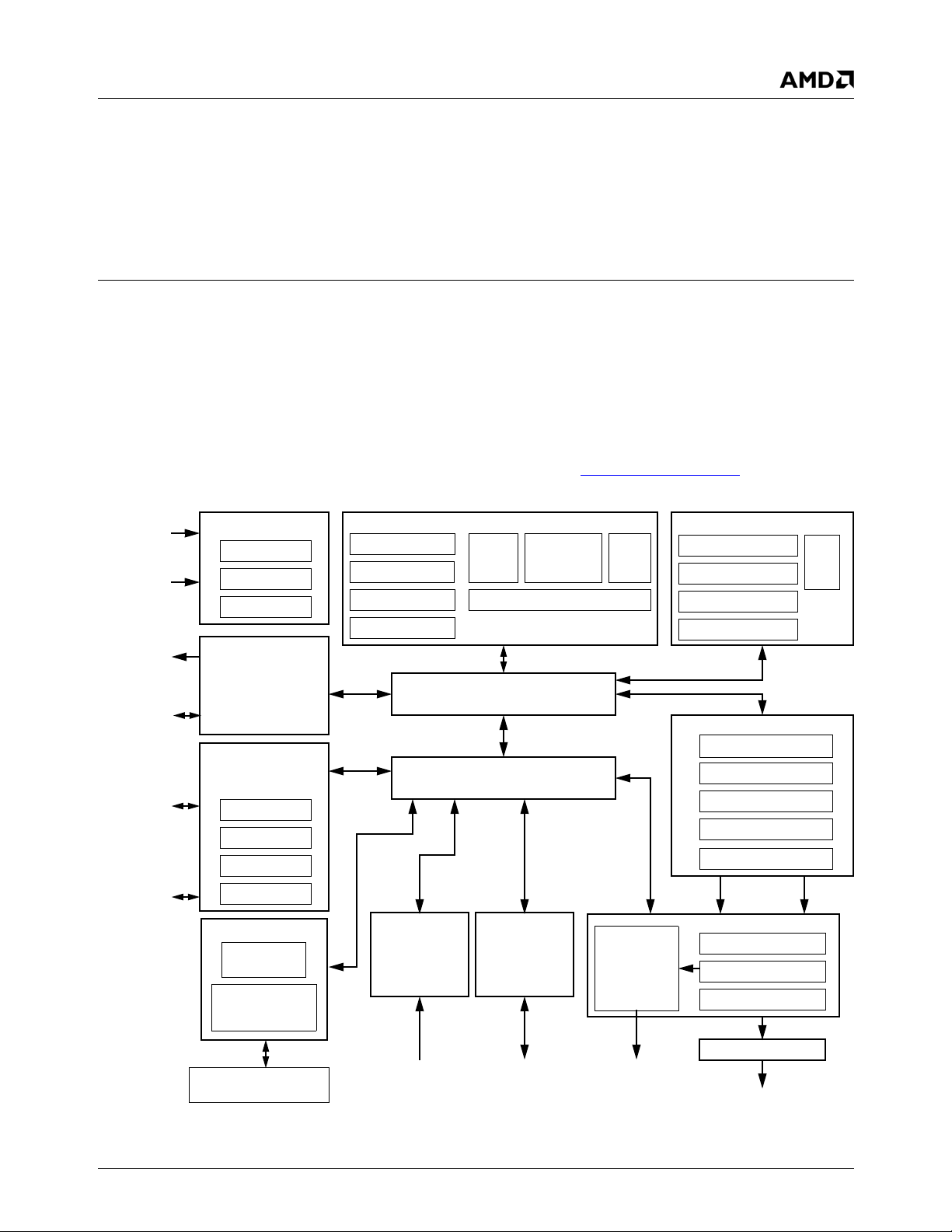
SYSREF
DOTREF
SDCLKs
64-Bit
DDR
Test/Reset
Interface
AMD Geode™
Companion
Device
Clock Module
System PLL
CPU PLL
DOTCLK PLL
GeodeLink™
Memory
Controller (GLMC)
64-bit DDR SDRAM
GeodeLink™
Control
Processor (GLCP)
Power Mgmnt
Te s t
Diagnostic
Companion I/F
Security Block
128-bit AES
(CBC/ECB)
Tr u e
Random Number
Generator
64 KB L1 I-cache
64 KB L1 D-cache
TLB
128 KB L2 cache
GeodeLink™ Interface Unit 0
GeodeLink™ Interface Unit 1
Video Input
Port (VIP)
CPU Core
Integer
Unit
(GLIU0)
(GLIU1)
GeodeLink™
Load/Store
Bus Controller
PCI Bridge
(GLPCI)
MMU
FPU
TFT
Controller/
Video
Output
Port (VOP)
Graphics Processor (GP)
BLT Engine
ROP Unit
Alpha Compositing
Rotation BLT
Display Controller (DC)
Compression Buffer
Palette RAM
Timing
Graphics Filter/Scaling
HW VGA
RGB YUV
Video Processor (VP)
Video Scalar
Video Mixer
Alpha Blender
1 KB
LUT
3x8-Bit DAC
EEPROM on package
(optional)
VIP
PCI
TFT/VOP
CRT
Figure 1-1. Internal Block Diagram
AMD Geode™ LX Processors Data Book 11
Page 12

33234H
Overview
1.2 Features
General Features
■ Functional blocks include:
—CPU Core
— GeodeLink™ Control Processor
— GeodeLink Interface Units
— GeodeLink Memory Controller
— Graphics Processor
— Display Controller
— Video Processor
– TFT Controller/Video Output Port
— Video Input Port
— GeodeLink PCI Bridge
— Security Block
■ 0.13 micron process
■ Packaging:
— 481-Terminal BGU (Ball Grid Array Cavity Up) with
internal heatspreader
■ Single packaging option supports all features
■ Industrial temperature range available for the
LX 800@0.9W processor*
CPU Processor Features
■ x86/x87-compatible CPU core
■ Performance:
— Processor frequency: up to 600 MHz
— Dhrystone 2.1 MIPs: 150 to 450
— Fully pipelined FPU
■ Split I/D cache/TLB (Translation Look-aside Buffer):
— 64 KB I-cache/64 KB D-cache
— 128 KB L2 cache configurable as I-cache, D-cache,
or both
■ Efficient prefetch and branch prediction
■ Integrated FPU that supports the MMX™ and
AMD 3DNow!™ instruction sets
■ Fully pipelined single precision FPU hardware with
microcode support for higher precisions
GeodeLink™ Control Processor
■ JTAG interface:
— ATPG, Full Scan, BIST on all arrays
— 1149.1 Boundary Scan compliant
■ ICE (in-circuit emulator) interface
■ Reset and clock control
■ Designed for improved software debug methods and
performance analysis
■ Power Management:
— LX 900@1.5W processor* (Unterminated):
Total Dissipated Power (TDP) 5.1W,
2.6W typical @ 600 MHz max power
— LX 800@0.9W processor* (Unterminated):
Total Dissipated Power (TDP) 3.6W,
1.8W typical @ 500 MHz max power
— LX 700@0.8W processor* (Unterminated):
Total Dissipated Power (TDP) 3.1W,
1.3W typical @ 433 MHz max power
— LX 600@0.7W processor* (Unterminated):
Total Dissipated Power (TDP) 2.8W,
1.2W typical @ 366 MHz max power
— GeodeLink active hardware power management
— Hardware support for standard ACPI software power
management
— I/O companion SUSP/SUSPA power controls
— Lower power I/O
— Wakeup on SMI/INTR
■ Works in conjunction with the AMD Geode™ CS5536
(USB 2.0) or CS5535 (USB 1.1) companion device
GeodeLink™ Architecture
■ High bandwidth packetized uni-directional bus for
internal peripherals
■ Standardized protocol to allow variants of products to be
developed by adding or removing modules
■ GeodeLink Control Processor (GLCP) for diagnostics
and scan control
■ Dual GeodeLink Interface Units (GLIUs) for device inter-
connect
GeodeLink™ Memory Controller
■ Integrated memory controller for low latency to CPU and
on-chip peripherals
■ 64-bit wide DDR SDRAM bus operating frequency:
— 200 MHz, 400 MT/S
■ Supports unbuffered DDR DIMMS using up to 2 GB
DRAM technology
■ Supports up to 2 DIMMS (16 devices max)
2D Graphics Processor
■ High performance 2D graphics controller
■ Alpha BLT
■ Windows
®
GDI GUI acceleration:
— Hardware support for all Microsoft RDP codes
■ Command buffer interface for asynchronous BLTs
■ Second pattern channel support
■ Hardware screen rotation
*The AMD Geode LX 900@1.5W processor operates at 600 MHz, the AMD Geode LX 800@0.9W processor operates at 500 MHz, the
AMD Geode LX 700@0.8W processor operates at 433 MHz and the AMD Geode LX 600@.07W processor operates at 366 MHz. Model
numbers reflect performance as described here: http://www.amd.com/connectivitysolutions/geodelxbenchmark
12 AMD Geode™ LX Processors Data Book
.
Page 13

Overview
33234H
Display Controller
■ Hardware frame buffer compression improves Unified
Memory Architecture (UMA) memory efficiency
■ CRT resolutions supported:
— Supports up to 1920x1440x32 bpp at 85 Hz
— Supports up to 1600x1200x32 bpp at 100 Hz
■ Supports up to 1600x1200x32 bpp at 60 Hz for TFT
■ Standard Definition (SD) resolution for Video Output
Port (VOP):
— 720x482 at 59.94 Hz interlaced for NTSC
— 768x576 at 50 Hz interlaced for PAL
■ High Definition (HD) resolution for Video Output Port
(VOP):
— Up to 1920x1080 at 30 Hz interlaced (1080i HD)
(74.25 MHz)
— Up to 1280x720 at 60 Hz progressive (720p HD)
(74.25 MHz)
■ Supports down to 7.652 MHz Dot Clock (320x240
QVGA)
■ Hardware VGA
■ Hardware supported 48x64 32-bit cursor with alpha
blending
GeodeLink™ PCI Bridge
■ PCI 2.2 compliant
■ 3.3V signaling and 3.3V I/Os
■ 33 to 66 MHz operation
■ 32-bit interface
■ Supports virtual PCI headers for GeodeLink devices
Video Input Port (VIP)
■ VESA 1.1 and 2.0 compliant, 8 or 16-bit
■ Video Blanking Interval (VBI) support
■ 8 or 16-bit 80 MHz SD or HD capable
Security Block
■ Serial EEPROM interface for 2K bit unique ID and AES
(Advanced Encryption Standard) hidden key storage
(EEPROM optional inside package)
■ Electronic Code Book (ECB) or Cipher Block Chaining
(CBC)128-bit AES hardware support
■ True random number generator (TRNG)
Video Processor
■ Supports video scaling, mixing and VOP
■ Hardware video up/down scalar
■ Graphics/video alpha blending and color key muxing
■ Digital VOP (SD and HD) or TFT outputs
■ Legacy RGB mode
■ VOP supports SD and HD 480p, 480i, 720p, and 1080i
■ VESA 1.1, 2.0 and BT.601 24-bit (out only), BT.656
compliant
Integrated Analog CRT DAC, System Clock PLLs and
Dot Clock PLL
■ Integrated Dot Clock PLL with up to 350 MHz clock
■ Integrated 3x8-bit DAC with up to 350 MHz sampling
■ Integrated x86 core PLL
■ Memory PLL
AMD Geode™ LX Processors Data Book 13
Page 14

33234H
Overview
14 AMD Geode™ LX Processors Data Book
Page 15

Architecture Overview 33234H
2.0Architecture Overview
2
The CPU Core provides maximum compatibility with the
vast amount of Internet content available while the intelligent integration of several other functions, including graphics, makes the AMD Geode™ LX processor a true systemlevel multimedia solution.
The AMD Geode LX processor can be divided into major
functional blocks (as shown in Figure 1-1 on page 11):
• CPU Core
• GeodeLink™ Control Processor
• GeodeLink Interface Units
• GeodeLink Memory Controller
• Graphics Processor
• Display Controller
• Video Processor
— TFT Controller/Video Output Port
• Video Input Port
• GeodeLink PCI Bridge
• Security Block
2.1 CPU Core
The x86 core consists of an Integer Unit, cache memory
subsystem, and an x87 compatible FPU (Floating Point
Unit). The Integer Unit contains the instruction pipeline and
associated logic. The memory subsystem contains the
instruction and data caches, translation look-aside buffers
(TLBs), and an interface to the GeodeLink Interface Units
(GLIUs).
The instruction set supported by the core is a combination
of Intel Pentium
AMD Geode LX processor specific instructions. Specifically, it supports the Pentium, Pentium Pro, AMD 3DNow!™
technology and MMX™ instructions for the AMD Athlon
processor. It supports a subset of the specialized
AMD Geode LX processor instructions including special
SMM instructions. The CPU Core does not support the
entire Katmai New Instruction (KNI) set as implemented in
the Pentium 3. It does support the MMX instructions for the
AMD Athlon processor, which are a subset of the
Pentium 3 KNI instructions.
®
processor, AMD Athlon™ processor, and
2.1.1 Integer Unit
The Integer Unit consists of a single issue 8-stage pipeline
and all the necessary support hardware to keep the pipeline running efficiently.
The instruction pipeline in the integer unit consists of eight
stages:
1) Instruction Prefetch - Raw instruction data is fetched
from the instruction memory cache.
2) Instruction Pre-decode - Prefix bytes are extracted
from raw instruction data. This decode looks-ahead to
the next instruction and the bubble can be squashed if
the pipeline stalls down stream.
3) Instruction Decode - Performs full decode of instruction data. Indicates instruction length back to the
Prefetch Unit, allowing the Prefetch Unit to shift the
appropriate number of bytes to the beginning of the
next instruction.
4) Instruction Queue - FIFO containing decoded x86
instructions. Allows Instruction Decode to proceed
even if the pipeline is stalled downstream. Register
reads for data operand address calculations are performed during this stage.
5) Address Calculation #1 - Computes linear address of
operand data (if required) and issues request to the
Data Memory Cache. Microcode can take over the
pipeline and inject a micro-box here if multi-box
instructions require additional data operands.
6) Address Calculation #2 - Operand data (if required)
is returned and set up to the Execution stage with no
bubbles if there was a data cache hit. Segment limit
checking is performed on the data operand address.
The µROM is read for setup to Execution Unit.
7) Execution Unit - Register and/or data memory fetch
fed through the Arithmetic Logic Unit (ALU) for arithmetic or logical operations. µROM always fires for the
first instruction box down the pipeline. Microcode can
take over the pipeline and insert additional boxes here
if the instruction requires multiple Execution Unit
stages to complete.
8) Writeback - Results of the Execution Unit stages are
written to the register file or to data memory.
AMD Geode™ LX Processors Data Book 15
Page 16

33234H
Architecture Overview
2.1.2 Memory Management Unit
The memory management unit (MMU) translates the linear
address supplied by the integer unit into a physical address
to be used by the cache unit and the internal bus interface
unit. Memory management procedures are x86-compatible, adhering to standard paging mechanisms.
The MMU also contains a load/store unit that is responsible
for scheduling cache and external memory accesses. The
load/store unit incorporates two performance-enhancing
features:
• Load-store reordering gives memory reads required by
the integer unit a priority over writes to external memory.
• Memory-read bypassing eliminates unnecessary
memory reads by using valid data from the execution
unit.
2.1.3 Cache and TLB Subsystem
The cache and TLB subsystem of the CPU Core supplies
the integer pipeline with instructions, data, and translated
addresses (when necessary). To support the efficient delivery of instructions, the cache and TLB subsystem has a
single clock access 64 KB 16-way set associative instruction cache and a 16-entry fully associative TLB. The TLB
performs necessary address translations when in protected
mode. For data, there is a 64 KB 16-way set associative
writeback cache, and a 16-entry fully associative TLB.
When there is a miss to the instruction or data TLBs, there
is a second level unified (instruction and data) 64-entry 2way set associative TLB that takes an additional clock to
access. When there is a miss to the instruction or data
caches or the TLB, the access must go to the GeodeLink
Memory Controller (GLMC) for processing. Having both an
instruction and a data cache and their associated TLBs
improves overall efficiency of the integer unit by enabling
simultaneous access to both caches.
The L1 caches are supported by a 128 KB unified L2 victim
cache. The L2 cache can be configured to hold data,
instructions, or both. The L2 cache is 4-way set associative.
integer core. The datapath is optimized for single precision
arithmetic. Extended precision instructions are handled in
microcode and require multiple passes through the pipeline. There is an execution pipeline and a load/store pipeline. This allows load/store operations to execute in parallel
with arithmetic instructions.
2.2 GeodeLink™ Control Processor
The GeodeLink Control Processor (GLCP) is responsible
for reset control, macro clock management, and debug
support provided in the Geode LX processor. It contains
the JTAG interface and the scan chain control logic. It supports chip reset, including initial PLL control and programming and runtime power management macro clock control.
The JTAG support includes a TAP Controller that is IEEE
1149.1 compliant. CPU control can be obtained through
the JTAG interface into the TAP Controller, and all internal
registers, including CPU Core registers, can be accessed.
In-circuit emulation (ICE) capabilities are supported
through this JTAG and TAP Controller interface.
The GLCP also includes the companion device interface.
The companion device has several unique signals connected to this module that support Geode LX processor
reset, interrupts, and system power management.
2.3 GeodeLink™ Interface Units
Together, the two GeodeLink Interface Units (GLIU0 and
GLIU1) make up the internal bus derived from the
GeodeLink architecture. GLIU0 connects five high bandwidth modules together with a seventh link to GLIU1 that
connects to the five low bandwidth modules.
2.4 GeodeLink™ Memory Controller
The GeodeLink Memory Controller (GLMC) is the source
for all memory needs in a typical Geode LX processor system. The GLMC supports a memory data bus width of 64
bits and supports 200 MHz, 400 MT/S for DDR (Double
Data Rate).
2.1.4 Bus Controller Unit
The bus controller unit provides a bridge from the processor to the GLIUs. When external memory access is
required, due to a cache miss, the physical address is
passed to the bus controller unit, that translates the cycle
to a GeodeLink cycle.
2.1.5 Floating Point Unit
The Floating Point Unit (FPU) is a pipelined arithmetic unit
that performs floating point operations as per the IEEE 754
standard. The instruction sets supported are x87, MMX,
and AMD 3DNow! technology. The FPU is a pipelined
machine with dynamic scheduling of instructions to minimize stalls due to data dependencies. It performs out of
order execution and register renaming. It is designed to
support an instruction issue rate of one per clock from the
16 AMD Geode™ LX Processors Data Book
The modules that need memory are the CPU Core, Graphics Processor, Display Controller, Video Input Port, and
Security Block. Because the GLMC supports memory
needs for both the CPU Core and the display subsystem,
the GLMC is classically called a UMA (Unified Memory
Architecture) subsystem. PCI accesses to main memory
are also supported.
Up to four banks, with eight devices maximum in each bank
of SDRAM, are supported with up to 512 MB in each bank.
Four banks means that one or two DIMM or SODIMM modules can be used in a AMD Geode LX processor system.
Some memory configurations have additional restrictions
on maximum device quantity.
Page 17
Architecture Overview
33234H
2.5 Graphics Processor
The Graphics Processor is based on the graphics processor used in the AMD Geode GX processor with several features added to enhance performance and functionality. Like
its predecessor, the AMD Geode LX processor’s Graphics
Processor is a BitBLT/vector engine that supports pattern
generation, source expansion, pattern/source transparency, 256 ternary raster operations, alpha blenders to support alpha-BLTs, incorporated BLT FIFOs, a GeodeLink
interface and the ability to throttle BLTs according to video
timing. Features added to the Graphics Processor include:
• Command buffer interface
• Hardware accelerated rotation BLTs
• Color depth conversion
• Paletized color
• Full 8x8 color pattern buffer
• Channel 3 - third DMA channel
• Monochrome inversion
Table 2-1 presents a comparison between the Graphics
Processor features of the AMD Geode GX and LX processors.
Table 2-1. Graphics Processor Feature Comparison
Feature AMD Geode™ GX Processor AMD Geode™ LX Processor
Color Depth 8, 16, 32 bpp 8, 16, 32 bpp (A) RGB 4 and 8-bit indexed
ROPs 256 (src, dest, pattern) 256 (2-src, dest and pattern)
BLT Buffers FIFOs in Graphics Processor FIFOs in Graphics Processor
BLT Splitting Managed by hardware Managed by hardware
Video Synchronized BLT/Vector Throttle by VBLANK Throttle by VBLANK
Bresenham Lines Yes Yes
Patterned (stippled) Lines No Yes
Screen to Screen BLT Yes Yes
Screen to Screen BLT with
mono expansion
Memory to Screen BLT Yes (through CPU writes) Yes (throttled rep movs writes)
Accelerated Text No No
Pattern Size (Mono) 8x8 pixels 8x8 pixels
Pattern Size (Color) 8x1 (32 pixels) 8x8 pixels
Monochrome Pattern Yes Yes (with inversion)
Dithered Pattern (4 color) No No
Color Pattern 8, 16, 32 bpp 8, 16, 32 bpp
Transparent Pattern Monochrome Monochrome
Solid Fill Yes Yes
Pattern Fill Yes Yes
Transparent Source Monochrome Monochrome
Color Key Source Transparency Y with mask Y with mask
Variable Source Stride Yes Yes
Variable Destination Stride Yes Yes
Destination Write Bursting Yes Yes
Selectable BLT Direction Vertical and Horizontal Vertical and Horizontal
Alpha BLT Yes (constant α or α/pix) Yes (constant α, α/pix, or sep. α channel)
VGA Support Decodes VGA Register Decodes VGA Register
Pipeline Depth 2 ops Unlimited
Accelerated Rotation BLT No 8, 16, 32 bpp
Color Depth Conversion No 5:6:5, 1:5:5:5, 4:4:4:4, 8:8:8:8
Ye s Ye s
8x2 (16 pixels)
8x4 (8 pixels)
AMD Geode™ LX Processors Data Book 17
Page 18

33234H
Architecture Overview
2.6 Display Controller
The Display Controller performs the following functions:
1) Retrieves graphics, video, and cursor data.
2) Serializes the streams.
3) Performs any necessary color lookups and output for-
matting.
4) Interfaces to the Video Processor for driving the dis-
play device(s).
The Display Controller consists of a memory retrieval system for rasterized graphics data, a VGA, and a back-end filter. The AMD Geode LX processor’s Display Controller
corresponds to the Display Controller function found in the
AMD Geode GX processor with additional hardware for
graphics filter functions. The VGA provides full hardware
compatibility with the VGA graphics standard. The rasterized graphics and the VGA share a single display FIFO and
display refresh memory interface to the GeodeLink Memory Controller (GLMC). The VGA uses 8 bpp and syncs,
that are expanded to 24 bpp via the color lookup table, and
passes the information to the graphics filter for scaling and
interlaced display support. The stream is then passed to
the Video Processor, which is used for video overlay. The
Video Processor forwards this information to the DAC (Digital-to-Analog Converter), that generates the analog red,
green, and blue signals, and buffers the sync signals that
are then sent to the display. The Video Processor output
can also be rendered as YUV data, and can be output on
the Video Output Port (VOP).
2.7 Video Processor
The Video Processor mixes the graphics and video
streams, and outputs either digital RGB data to the internal
DACs or the flat panel interface, or digital YUV data via the
VOP interface.
The Video Processor delivers high-resolution and truecolor graphics. It can also overlay or blend a scaled truecolor video image on the graphic background.
The Video Processor interfaces with the CPU Core via a
GLIU master/slave interface. The Video Processor is a
slave only, as it has no memory requirements.
2.7.2 TFT Controller
The TFT Controller converts the digital RGB output of a
Video Mixer block to the digital output suitable for driving a
TFT flat panel LCD.
The flat panel connects to the RGB port of the Video Mixer.
It interfaces directly to industry standard 18-bit or 24-bit
active matrix thin film transistor (TFT). The digital RGB or
video data that is supplied by the video logic is converted
into a suitable format to drive a wide range of panels with
variable bits. The LCD interface includes dithering logic to
increase the apparent number of colors displayed for use
on panels with less than 6 bits per color. The LCD interface
also supports automatic power sequencing of panel power
supplies.
It supports panels up to a 24-bit interface and up to
1600x1200 resolution.
The TFT Controller interfaces with the CPU Core via a
GLIU master/slave interface. The TFT Controller is both a
GLIU master and slave.
2.7.3 Video Output Port
The VOP receives YUV 4:4:4 encoded data from the Video
Processor and formats the data into a video stream that is
BT.656 compliant. Output from the VOP goes to either a
VIP or a TV encoder. The VOP is BT.656/601 compliant
since its output may go directly (or indirectly) to a display.
2.8 Video Input Port
The Video Input Port (VIP) receives 8- or 16-bit video or
ancillary data, 8-bit message data, or 8-bit raw video and
passes it to data buffers located in system memory. The
VIP is a DMA engine. The primary operational mode is as a
compliant VESA 2.0 slave. The VESA 2.0 specification
defines the protocol for receiving video, VBI, and ancillary
data. The addition of the message passing and data
streaming modes provides additional flexibility in receiving
non-VESA 2.0 compliant data streams. Input data is
packed into QWORDS, buffered into a FIFO, and sent to
system memory over the GLIU. The VIP masters the internal GLIU and transfers the data from the FIFO to system
memory. The maximum input data rate (8- or 16-bits) is 150
MHz.
2.7.1 CRT Interface
The internal high performance DACs support CRT resolutions up to:
— 1920x1440x32 bpp at 85 Hz
— 1600x1200x32 bpp at 100 Hz
18 AMD Geode™ LX Processors Data Book
2.9 GeodeLink™ PCI Bridge
The GeodeLink PCI Bridge (GLPCI) contains all the necessary logic to support an external PCI interface. The PCI
interface is PCI v2.2 specification compliant. The logic
includes the PCI and GLIU interface control, read and write
FIFOs, and a PCI arbiter.
Page 19

Architecture Overview
33234H
2.10 Security Block
The AMD Geode LX processor has an on-chip AES 128-bit
crypto acceleration block capable of 44 Mbps throughput
on either encryption or decryption at a processor speed of
500 MHz. The AES block runs asynchronously to the processor core and is DMA based. The AES block supports
both EBC and CBC modes and has an interface for
accessing the optional EEPROM memory for storing
unique IDs and/or security keys. The AES and EEPROM
sections have separate control registers but share a single
set of interrupt registers. The AES module has two key
sources: one hidden 128-bit key stored in the “on-package”
EEPROM, and a write only 128-bit key (reads as all zeros).
The hidden key is loaded automatically by the hardware
after reset and is not visible to the processor. The
EEPROM can be locked. The initialization vector for the
CBC mode can be generated by the True Random Number
Generator (TRNG). The TRNG is addressable separately
and generates a 32-bit random number.
AMD Geode™ LX Processors Data Book 19
Page 20

33234H
Architecture Overview
20 AMD Geode™ LX Processors Data Book
Page 21
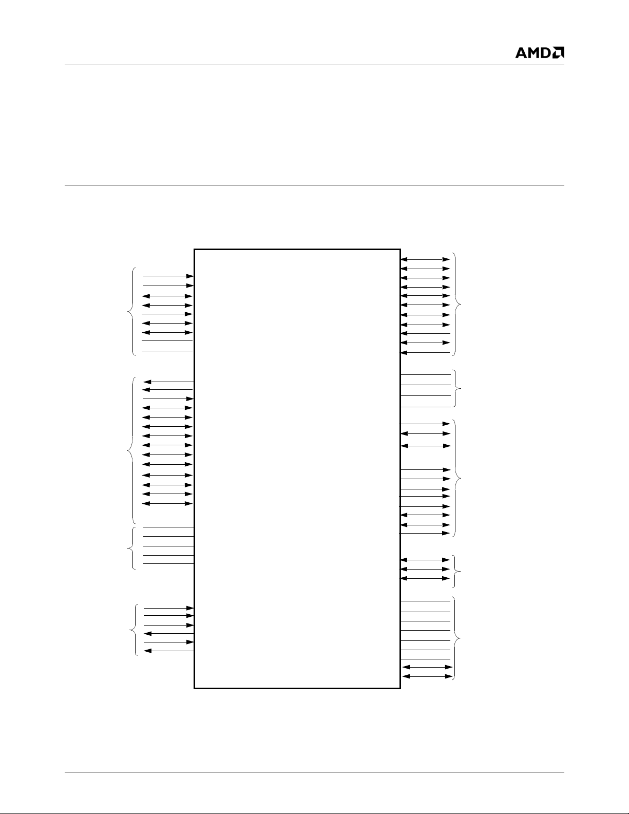
Signal Definitions 33234H
3.0Signal Definitions
3
This chapter defines the signals and describes the external interface of the AMD Geode™ LX processor. Figure 3-1 shows
the pins organized by their functional groupings. Where signals are multiplexed, the default signal name is listed first and is
separated by a plus sign (+). Multi-function pins are described in Table 3-1 on page 22.
AD[31:0]
CBE[3:0]#
FRAME#
IRDY#
TRDY#
STOP#
DEVSEL#
PA R
REQ[2:0]#
GNT[2:0]#
RESET#
PCI
Interface
Signals
System
Interface
Signals
SYSREF
DOTREF
INTA#
IRQ13 (STRAP)
CIS
SUSPA# (STRAP)
PW[1:0] (STRAP)
TDP
TDN
AMD Geode™
LX Processor
(STRAP)
Memory
Interface
Signals
PLL
Interface
Signals
Internal Test
and
Measurement
Interface
Signals
SDCLK[5:0]P
SDCLK[5:0]N
MVREF
CKE[1:0]
CS[3:0]#
RAS[1:0]#
CAS[1:0]#
WE[1:0]#
BA[1:0]
MA[13:0]
TLA[1:0]
DQS[7:0]
DQM[7:0]
DQ[63:0]
VAVDD, CAVDD, MAV
VAVSS, CAVSS, MAV
CLPF
MLPF
VLPF
TCLK
TMS
TDI
TDO
TDBGI
TDBGO
DD
SS
(Total of 32) V
(Total of 30) V
(Total of 33) V
(Total of 128) V
DOTCLK+VOPCLK
DRGB[31:26]+VID[15:10]
DRGB[25:24]+VID[9:8]+
MSGSTART+MSGSTOP
DRBG[15:8]+VOP[15:8]
DRGB[7:0]+VOP[7:0]
HSYNC+VOP_HSYNC
VSYNC+VOP_VSYNC
VDDEN+VIP_HSYNC
LDEMOD+VIP_VSYNC
DISPEN+VOP_BLANK
(Total of 4) DAV
(Total of 4) DAV
CORE
MEM
SS
DRGB[23:16]
VIPCLK
VID[7:0]
VIPSYNC
DVR EF
DRSET
DD
SS
RED
GREEN
BLUE
HSYNC
VSYNC
IO
Power/Ground
Interface
Signals
Display (TFT Option)
Interface
Signals
VIP
Interface
Signals
Display (CRT Option)
Interface
Signals
Figure 3-1. Signal Groups
AMD Geode™ LX Processors Data Book 21
Page 22
33234H
Signal Definitions
Table 3-1. Video Signal Definitions Per Mode
Signal Name CRT w/16-bit VIP
RED RED
GREEN GREEN
BLUE BLUE
DRGB[31:24] (I/O) VID[15:8] (I) VID[15:8] (I) Alpha VID[15:8] (I) VID[15:8] (I)
DRGB[23:16] (O) R[7:0] R[7:0] R[7:0] R[7:0] (Note 2) Driven low
DRGB[15:8] (O) G[7:0] G[7:0] G[7:0] G[7:0] (Note 2) VOP[15:8] (O)
DRGB[7:0] (O) B[7:0] B[7:0] B[7:0] B[7:0] (Note 2) VOP[7:0] (O)
DOTCLK (O) DOTCLK (O) DOTCLK (O) DOTCLK (O) DOTCLK (O) VOPCLK (O)
HSYNC (O) HSYNC (O) HSYNC (O) HSYNC (O) VOP_HSYNC (O) VOP_HSYNC (O)
VSYNC (O) VSYNC (O) VSYNC (O) VSYNC (O) VSYNC (O) VOP_VSYNC (O)
DISPEN (O) DISPEN (O) VOP_BLANK (O)
VDDEN (I/O) VIP_HSYNC (I) VIP_HSYNC (I) VIP_HSYNC (I) VDDEN (O) VIP_HSYNC (I)
LDEMOD (I/O) VIP_VSYNC (I) VIP_VSYNC (I) VIP_VSYNC (I) LDEMOD (O) VIP_VSYNC (I)
VID[7:0] (I) VID[7:0] VID[7:0] VID[7:0] VID[7:0] VID[7:0]
VIPCLK (I) VIPCLK VIPCLK VIPCLK VIPCLK VIPCLK
VIPSYNC (I) VIPSYNC VIPSYNC VIPSYNC VIPSYNC VIPSYNC
Note 1. Alpha RED/GREEN/BLUE: Useful for off-chip graphics digital interfaces.
Note 2. Pin usage depends on TFT mode. See Section 6.7.7 "Flat Panel Display Controller" on page 405 for details.
RGB w/16-bit
VIP
ARGB (Note 1)
w/8-bit VIP
TFT w/16-bit VIP
(not 601)
8- or 16-bit VOP
w/16-bit VIP
22 AMD Geode™ LX Processors Data Book
Page 23
Signal Definitions
33234H
3.1 Buffer Types
The Ball Assignment tables starting on page 26 include a
column labeled “Buffer Type”. The details of each buffer
type listed in this column are given in Table 3-2. The column headings in Table 3-2 are identified as follows:
TS: Indicates whether the buffer may be put into the TRISTATE mode. Note some pins that have buffer types that
allow TRI-STATE may never actually enter the TRI-STATE
mode in practice, since they may be inputs or provide other
signals that are always driven. To determine if a particular
signal can be put in the TRI-STATE mode, consult the individual signal descriptions in Section 3.4 "Signal Descriptions" on page 33.
OD: Indicates if the buffer is open-drain, or not. Open-drain
outputs may be wire ORed together and require a discrete
pull-up resistor to operate properly.
5VT: Indicates if the buffer is 5-volt tolerant, or not. If it is 5volt tolerant, then 5 volt TTL signals may be safely applied
to this pin.
PU/PD: Indicates if an internal, programmable pull-up or
pull-down resistor may be present.
Current High/Low (mA): This column gives the current
source/sink capacities when the voltage at the pin is high,
and low. The high and low values are separated by a “/”
and values given are in milli-amps (mA).
Rise/Fall @ Load: This column indicates the rise and fall
times for the different buffer types at the load capacitance
indicated. These measurements are given in two ways:
rise/fall time between the 20%-80% voltage levels, or, the
rate of change the buffer is capable of, in volts-per-nanosecond (V/ns).
Note the presence of “Wire” type buffer in this table. Signals identified as a wire-type are not driven by a buffer,
hence no rise/fall time or other measurements are given;
these are marked “NA” in Table 3-2. The wire-type connection indicates a direct connection to internal circuits such
as power, ground, and analog signals.
Table 3-2. Buffer Type Characteristics
Name TS OD 5VT PU/PD
Current
High/Low
(mA) Rise/Fall @ Load
24/Q3 X X 24/24 3 ns @ 50 pF
24/Q5 X X 24/24 5 ns @ 50 pF
24/Q7 X X 24/24 7 ns @ 50 pF
5V X X 16/16 1.25V/ns @ 40 pF
PCI X 0.5/1.5 1-4V/ns @ 10 pF
DDRCLK 10/10 8.5V/ns @ 15 pF
DDR 2.4V/ns @ 50 pF
Wire NA NA NA NA NA
AMD Geode™ LX Processors Data Book 23
Page 24
33234H
Signal Definitions
3.2 Bootstrap Options
The bootstrap options shown in Table 3-3 are supported in
the AMD Geode LX processor for configuring the system.
Table 3-3. Bootstrap Options
Pins Description
IRQ13 0: Normal boot operation, TAP reset
active during PCI reset
1: Debug stall of CPU after CPU
reset, TAP reset active until V
PW1 0: PCI (SYSREF) is 33 MHz
1: PCI (SYSREF) is 66 MHz
PW0,
SUSPA#,
GNT[2:0]#
Select CPU and GeodeLink system
MHz options including a PLL bypass
option. Refer to Table 6-87 on page
556 for programming.
IO
valid
3.3 Ball Assignments
The tables in this chapter use several common abbreviations. Table 3-4 lists the mnemonics and their meanings.
Table 3-4. Ball Type Definitions
Mnemonic Definition
AAnalog
I Input ball
I/O Bidirectional ball
CAV
SS
CAV
DD
DAV
SS
DAV
DD
MAV
SS
MAV
DD
O Output ball
VAV
SS
VAV
DD
V
CORE
V
IO
V
MEM
V
SS
# The “#” symbol at the end of a signal
Core PLL Ground ball: Analog
Core PLL Power ball: Analog
DAC PLL Ground ball: Analog
DAC PLL Power ball: Analog
GLIU PLL Ground ball: Analog
GLIU PLL Power ball: Analog
Video PLL Ground ball: Analog
Video PLL Power ball: Analog
Power ball: 1.2V (Nominal)
I/O Power ball: 3.3V (Nominal)
Power ball: 2.5V
Ground ball
name indicates that the active, or
asserted state, occurs when the signal is at a low voltage level. When “#”
is not present after the signal name,
the signal is asserted when at a high
voltage level.
24 AMD Geode™ LX Processors Data Book
Page 25
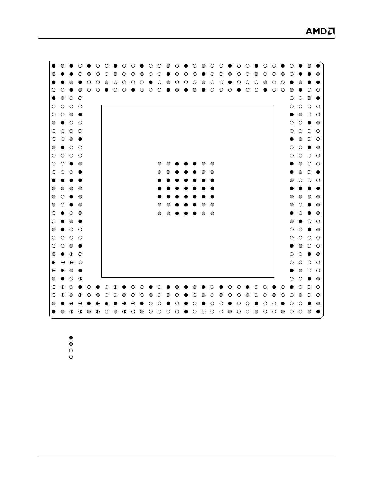
Signal Definitions
33234H
12345678910111213141516171819202122232425262728293031
A
VSSV
B
V
MEMVSSVSS
C
VSSVSSV
D
DQ20 DQ16 VSSV
E
V
SSVMEM
F
DQ15 DQ14 DQ10 CKE1
G
DQ13 DQM1 V
H
V
MEMVSS
J
DQ9 DQ8 DQ12 SDK1P
K
DQ7 DQ3 V
L
V
MEMVSS
M
DQM0 DQS0 DQ2 SDK0P
N
DQ5 DQ1 V
P
MVREF DQ0 DQ4 V
R
VSSVSSVSSV
T
V
COREVCOREVCOREVCORE
U
DAVDDBLUE DAVSSV
V
DAVDDGREEN DAVSSDAV
W
DVRE F DAVSSRED DAV
Y
DRSET DAVSSVIOV
AA
VAVDDVAVSSVLPF T MS
AB
DOTREF TDBGI TDI TDBGO
AC
TDO TCLK V
AD
VIOVSSVSYNC LDEMOD
AE
DOTCLK VD EN HSYNC DISPEN
AF
DRB17 DRB16 V
AG
VIOVSSDRB18 DRB19
AH
DRB20 DRB21 DRB22 VSSDRB11 VSSDRB0 DRB6 VSSDRB29 DRB24 VSSVID3 VSSV
AJ
DRB23 DR B8 V
AK
V
IOVSS
AL
VSSVIODRB10 DRB13 VIODRB2 DRB5 VIODRB30 DRB27 VIOVIPCLK VID6 VIPSYNC VID2 VSSTDP PW0 AD7 AD2 VIOAD9 AD12 VIOAD13 CBE1# VIOFRAME# AD18 VIOV
DQ21 VSSDQM2 DQ22 VSSDQ28 DQS3 VSSDQ26 DQ31 V
MEMVSS
DQ17 V
DQ18 DQ23 V
MEM
MA12 DQ S2 V
MEMVSS
MA11 MA9 VSSMA7 MA8 VSSMA5 MA6 MA4 VSSV
MEM
DQ11 CKE0 CAS0# CAS1# V
MEMVSS
DQS1 SDK1N
MEMVSS
DQ6 SDK0N
SSVMEM
SS
SS
CORE
DD
DD
SS
DQ24 DQM3 V
MEM
DQ19 DQ29 DQ25 DQ30 VSSMA3 V
MEM
DQ27 TLA1 VSSTLA0 DQ36 DQ33 VSSDQ34 DQ38 V
MEM
AMD Geode™
LX Processor
IOVSS
IOVSS
DRB12 DRB15 VIODRB3 DRB7 VIODRB28 DRB25 VIOVID4 VIOVID0 VSSPW1 VIOAD0 VIOAD6 CBE0# VIOAD15 STOP# VIOPAR A D 1 6 VIOAD19 AD21
IO
DRB9 DRB14 VSSDRB1 DRB4 VSSDRB31 DRB26 VSSVID7 VID5 VSSVID1 VSSTDN VSSAD4 AD3 VSSAD8 AD10 VSSDEVSL# TRDY# VSSAD17 AD20 VSSV
DQ32 VSSDQ37 V
MEM
MA2 MA0 MA1 V
MEM
COREVSSVCOREVSS
V
COREVCOREVSSVSSVSSVCOREVCORE
V
COREVCOREVSSVSSVSSVCOREVCORE
VSSVSSVSSVSSVSSVSSV
VSSVSSVSSVSSVSSVSSV
VSSVSSVSSVSSVSSVSSV
V
COREVCOREVSSVSSVSSVCOREVCORE
V
COREVCOREVSSVSSVSSVCOREVCORE
DQM4 DQ39 VSSDQ40 DQ41 VSSDQ42 DQ43 VSSWE1# VSSV
MEM
MEM
(Top View)
COREVSSVCOREVSS
s
s
DQ35 DQS5 V
MEM
DQS4 BA1 VSSDQ44 DQ45 DQM5 V
MA10 SD K5PS DK5N VSSSDK4P SDK4N VSSBA0 RAS1# V
SS
SS
SS
AD1 VSSAD5 AD11 VSSAD14 IRDY# VSSCBE2# VSSAD23 AD22 CBE3#
DQ46 DQ47 V
MEM
MEM
CS0# VSSVSSV
MEM
RAS0# WE0# VSSV
MEMVSS
CS1# CS2# MA13 DQ49
VSSV
SDK3N DQM6 V
SDK3P DQS6 DQ55 DQ54
VSSV
SDK2N DQ60 V
SDK2P DQ61 DQ57 DQ56
VSSV
V
SSVMEM
V
CORE
V
SSVSSVSSVSS
V
COREVCOREVCOREVCORE
V
CORE
VSSCLPF CAVSSCAV
V
COREVSS
s
GNT0# REQ0# V
REQ2# IRQ13 GNT1# REQ1#
V
SSVIO
INTA# AD31 V
AD27 CIS AD29 AD30
V
SSVIO
AD25 AD24 V
12345678910111213141516171819202122232425262728293031
Note: Signal names have been abbreviated in this figure due to space constraints.
= GND Ball
= PWR Ball
S
= Strap Option Ball
= Multiplexed Ball
MEMVSS
MEM
MEMVSSVSS
CS3# DQ48
MEMVSS
DQ52 DQ53
MEM
SSVMEM
DQ50 DQ51
MEM
SSVMEM
DQM7 DQS7
MEM
DQ62 V
DQ63 DQ58 DQ59
MLPF MAVSSMAV
RESET# SYREF
SSVIO
s
s
GNT2# SUPA#
SSVIO
AD26 AD28
SSVIO
A
B
C
D
E
F
G
H
J
K
L
M
N
P
SS
R
T
U
V
DD
W
DD
Y
AA
AB
ss
AC
AD
AE
AF
AG
AH
AJ
AK
IO
AL
SS
Figure 3-2. BGU481 Ball Assignment Diagram
AMD Geode™ LX Processors Data Book 25
Page 26
33234H
Table 3-5. Ball Assignments - Sorted by Ball Number
Ball
Signal Name
No.
(Note 1)
A1 V
SS
A2 V
MEM
A3 V
SS
A4 DQ21 I/O DDR
A5 V
SS
A6 DQM2 I/O DDR
A7 DQ22 I/O DDR
A8 V
SS
A9 DQ28 I/O DDR
A10 DQS3 I/O DDR
A11 V
SS
A12 DQ26 I/O DDR
A13 DQ31 I/O DDR
A14 V
MEM
A15 DQ32 I/O DDR
A16 V
SS
A17 DQ37 I/O DDR
A18 V
MEM
A19 DQM4 I/O DDR
A20 DQ39 I/O DDR
A21 V
SS
A22 DQ40 I/O DDR
A23 DQ41 I/O DDR
A24 V
SS
A25 DQ42 I/O DDR
A26 DQ43 I/O DDR
A27 V
SS
A28 WE1# I/O DDR
A29 V
SS
A30 V
MEM
A31 V
SS
B1 V
MEM
B2 V
SS
B3 V
SS
B4 DQ17 I/O DDR
B5 V
MEM
B6 DQ18 I/O DDR
B7 DQ23 I/O DDR
B8 V
MEM
B9 DQ24 I/O DDR
B10 DQM3 I/O DDR
B11 V
MEM
B12 DQ27 I/O DDR
B13 TLA1 I/O DDR
B14 V
SS
B15 TLA0 I/O DDR
B16 DQ36 I/O DDR
B17 DQ33 I/O DDR
B18 V
SS
Typ e
Buffer
(PD)
Typ e
GND ---
PWR ---
GND ---
GND ---
GND ---
GND ---
PWR ---
GND ---
PWR ---
GND ---
GND ---
GND ---
GND ---
PWR ---
GND ---
PWR ---
GND ---
GND ---
PWR ---
PWR ---
PWR ---
GND ---
GND ---
Ball
No.
Signal Name
(Note 1)
Typ e
(PD)
Buffer
Typ e
B19 DQ34 I/O DDR
B20 DQ38 I/O DDR
B21 V
MEM
PWR ---
B22 DQ35 I/O DDR
B23 DQS5 I/O DDR
B24 V
MEM
PWR ---
B25 DQ46 I/O DDR
B26 DQ47 I/O DDR
B27 V
MEM
PWR ---
B28 CS0# I/O DDR
B29 V
B30 V
B31 V
C1 V
C2 V
C3 V
C4 V
SS
SS
MEM
SS
SS
MEM
SS
GND ---
GND ---
PWR ---
GND ---
GND ---
PWR ---
GND ---
C5 MA12 I/O DDR
C6 DQS2 I/O DDR
C7 V
MEM
PWR ---
C8 DQ19 I/O DDR
C9 DQ29 I/O DDR
C10 DQ25 I/O DDR
C11 DQ30 I/O DDR
C12 V
SS
GND ---
C13 MA3 I/O DDR
C14 V
MEM
PWR ---
C15 MA2 I/O DDR
C16 MA0 I/O DDR
C17 MA1 I/O DDR
C18 V
MEM
PWR ---
C19 DQS4 I/O DDR
C20 BA1 I/O DDR
C21 V
SS
GND ---
C22 DQ44 I/O DDR
C23 DQ45 I/O DDR
C24 DQM5 I/O DDR
C25 V
MEM
PWR ---
C26 RAS0# I/O DDR
C27 WE0# I/O DDR
C28 V
C29 V
C30 V
C31 V
SS
MEM
SS
SS
GND ---
PWR ---
GND ---
GND ---
D1 DQ20 I/O DDR
D2 DQ16 I/O DDR
D3 V
D4 V
SS
MEM
GND ---
PWR ---
D5 MA11 I/O DDR
D6 MA9 I/O DDR
Signal Definitions
Ball
Signal Name
No.
(Note 1)
D7 V
SS
D8 MA7 I/O DDR
D9 MA8 I/O DDR
D10 V
SS
D11 MA5 I/O DDR
D12 MA6 I/O DDR
D13 MA4 I/O DDR
D14 V
SS
D15 V
CORE
D16 V
SS
D17 V
CORE
D18 V
SS
D19 MA10 I/O DDR
D20 SDCLK5P O DDRCLK
D21 SDCLK5N O DDRCLK
D22 V
SS
D23 SDCLK4P O DDRCLK
D24 SDCLK4N O DDRCLK
D25 V
SS
D26 BA0 I/O DDR
D27 RAS1# I/O DDR
D28 V
MEM
D29 V
SS
D30 CS3# I/O DDR
D31 DQ48 I/O DDR
E1 V
SS
E2 V
MEM
E3 DQ11 I/O DDR
E4 CKE0 I/O DDR
E28 CAS0# I/O DDR
E29 CAS1# I/O DDR
E30 V
MEM
E31 V
SS
F1 DQ15 I/O DDR
F2 DQ14 I/O DDR
F3 DQ10 I/O DDR
F4 CKE1 I/O DDR
F28 CS1# I/O DDR
F29 CS2# I/O DDR
F30 MA13 I/O DDR
F31 DQ49 I/O DDR
G1 DQ13 I/O DDR
G2 DQM1 I/O DDR
G3 V
MEM
G4 V
SS
G28 V
SS
G29 V
MEM
G30 DQ52 I/O DDR
G31 DQ53 I/O DDR
H1 V
MEM
Typ e
Buffer
(PD)
Typ e
GND ---
GND ---
GND ---
PWR ---
GND ---
PWR ---
GND ---
GND ---
GND ---
PWR ---
GND ---
GND ---
PWR ---
PWR ---
GND ---
PWR ---
GND ---
GND ---
PWR ---
PWR ---
26 AMD Geode™ LX Processors Data Book
Page 27
Signal Definitions
Table 3-5. Ball Assignments - Sorted by Ball Number (Continued)
Ball
Signal Name
No.
(Note 1)
H2 V
SS
H3 DQS1 I/O DDR
H4 SDCLK1N O DDRCLK
H28 SDCLK3N O DDRCLK
H29 DQM6 I/O DDR
H30 V
SS
H31 V
MEM
J1 DQ9 I/O DDR
J2 DQ8 I/O DDR
J3 DQ12 I/O DDR
J4 SDCLK1P O DDRCLK
J28 SDCLK3P O DDRCLK
J29 DQS6 I/O DDR
J30 DQ55 I/O DDR
J31 DQ54 I/O DDR
K1 DQ7 I/O DDR
K2 DQ3 I/O DDR
K3 V
MEM
K4 V
SS
K28 V
SS
K29 V
MEM
K30 DQ50 I/O DDR
K31 DQ51 I/O DDR
L1 V
MEM
L2 V
SS
L3 DQ6 I/O DDR
L4 SDCLK0N O DDRCLK
L28 SDCLK2N O DDRCLK
L29 DQ60 I/O DDR
L30 V
SS
L31 V
MEM
M1 DQM0 I/O DDR
M2 DQS0 I/O DDR
M3 DQ2 I/O DDR
M4 SDCLK0P O DDRCLK
M28 SDCLK2P O DDRCLK
M29 DQ61 I/O DDR
M30 DQ57 I/O DDR
M31 DQ56 I/O DDR
N1 DQ5 I/O DDR
N2 DQ1 I/O DDR
N3 V
SS
N4 V
MEM
N13 V
CORE
N14 V
CORE
N15 V
SS
N16 V
SS
N17 V
SS
N18 V
CORE
N19 V
CORE
Typ e
Buffer
(PD)
GND ---
GND ---
PWR ---
PWR ---
GND ---
GND ---
PWR ---
PWR ---
GND ---
GND ---
PWR ---
GND ---
PWR ---
PWR ---
PWR ---
GND ---
GND ---
GND ---
PWR ---
PWR ---
Typ e
Ball
No.
N28 V
N29 V
Signal Name
(Note 1)
SS
MEM
Typ e
(PD)
Buffer
Typ e
GND ---
PWR ---
N30 DQM7 I/O DDR
N31 DQS7 I/O DDR
P1 MVREF I ---
P2 DQ0 I/O DDR
P3 DQ4 I/O DDR
P4 V
P13 V
P14 V
P15 V
P16 V
P17 V
P18 V
P19 V
P28 V
P29 V
SS
CORE
CORE
SS
SS
SS
CORE
CORE
SS
MEM
GND ---
PWR ---
PWR ---
GND ---
GND ---
GND ---
PWR ---
PWR ---
GND ---
PWR ---
P30 DQ62 I/O DDR
P31 V
R1 V
R2 V
R3 V
R4 V
R13 V
R14 V
R15 V
R16 V
R17 V
R18 V
R19 V
R28 V
SS
SS
SS
SS
SS
SS
SS
SS
SS
SS
SS
SS
CORE
GND ---
GND ---
GND ---
GND ---
GND ---
GND ---
GND ---
GND ---
GND ---
GND ---
GND ---
GND ---
PWR ---
R29 DQ63 I/O DDR
R30 DQ58 I/O DDR
R31 DQ59 I/O DDR
T1 V
T2 V
T3 V
T4 V
T13 V
T14 V
T15 V
T16 V
T17 V
T18 V
T19 V
T28 V
T29 V
T30 V
CORE
CORE
CORE
CORE
SS
SS
SS
SS
SS
SS
SS
SS
SS
SS
PWR ---
PWR ---
PWR ---
PWR ---
GND ---
GND ---
GND ---
GND ---
GND ---
GND ---
GND ---
GND ---
GND ---
GND ---
33234H
Ball
Signal Name
No.
(Note 1)
T31 V
SS
U1 DAV
DD
U2 BLUE A ---
U3 DAV
U4 V
U13 V
U14 V
U15 V
U16 V
U17 V
U18 V
U19 V
U28 V
U29 V
U30 V
U31 V
V1 DAV
SS
CORE
SS
SS
SS
SS
SS
SS
SS
CORE
CORE
CORE
CORE
DD
V2 GREEN A ---
V3 DAV
V4 DAV
V13 V
V14 V
V15 V
V16 V
V17 V
V18 V
V19 V
V28 V
SS
DD
CORE
CORE
SS
SS
SS
CORE
CORE
CORE
V29 MLPF A ---
V30 MAV
V31 MAV
SS
DD
W1 DVREF A ---
W2 DAV
SS
W3 RED A ---
W4 DAV
W13 V
W14 V
W15 V
W16 V
W17 V
W18 V
W19 V
W28 V
DD
CORE
CORE
SS
SS
SS
CORE
CORE
SS
W29 CLPF A ---
W30 CAV
W31 CAV
SS
DD
Y1 DRSET A ---
Typ e
Buffer
(PD)
Typ e
GND ---
APWR ---
AGND ---
PWR ---
GND ---
GND ---
GND ---
GND ---
GND ---
GND ---
GND ---
PWR ---
PWR ---
PWR ---
PWR ---
APWR ---
AGND ---
APWR ---
PWR ---
PWR ---
GND ---
GND ---
GND ---
PWR ---
PWR ---
PWR ---
AGND ---
APWR ---
AGND ---
APWR ---
PWR ---
PWR ---
GND ---
GND ---
GND ---
PWR ---
PWR DDR
GND ---
AGND ---
APWR ---
AMD Geode™ LX Processors Data Book 27
Page 28
33234H
Table 3-5. Ball Assignments - Sorted by Ball Number (Continued)
Ball
Signal Name
No.
(Note 1)
Y2 DAV
Y3 V
Y4 V
Y28 V
Y29 V
SS
IO
SS
CORE
SS
Y30 RESET# I PCI
Y31 SYSREF I PCI
AA1 VAV
AA2 VAV
DD
SS
AA3 VLPF A ---
AA4 TMS I 24/Q7
AA28 GNT0# I/O PCI
AA29 REQ0# I PCI
AA30 V
AA31 V
SS
IO
AB1 DOTREF I PCI
AB2 TDBGI I 24/Q7
AB3 TDI I 24/Q7
AB4 TDBGO O (PD) 24/Q3
AB28 REQ2# I/O PCI
AB29 IRQ13 I/O (PD) 24/Q5
AB30 GNT1# I/O PCI
AB31 REQ1# I/O PCI
AC1 TDO O 24/Q5
AC2 TCL K I 24/Q7
AC3 V
IO
AC4 V
SS
AC28 V
AC29 V
SS
IO
AC30 GNT2# I/O PCI
AC31 SUSPA# I/O 24/Q5
AD1 V
IO
AD2 V
SS
AD3 VSYNC O (PD) 5V
VOP_VSYNC O
AD4 LDEMOD I/O (PD) 24/Q5
VIP_VSYNC I
AD28 INTA# I/O (PD) 24/Q5
AD29 AD31 I/O PCI
AD30 V
AD31 V
SS
IO
AE1 DOTCLK O (PD) 24/Q3
VOPCLK O
AE2 VDDEN I/O (PD) 24/Q5
VIP_HSYNC I
AE3 HSYNC O (PD) 5V
VOP_HSYNC O
AE4 DISPEN O (PD) 24/Q5
VOP_BLANK O
AE28 AD27 I/O PCI
Typ e
Buffer
(PD)
Typ e
AGND ---
PWR ---
GND ---
PWR ---
GND ---
APWR ---
AGND ---
GND ---
PWR ---
PWR ---
GND ---
GND ---
PWR ---
PWR ---
GND ---
GND ---
PWR ---
Ball
No.
Signal Name
(Note 1)
Typ e
(PD)
Buffer
Typ e
AE29 CIS I/O 24/Q7
AE30 AD29 I/O PCI
AE31 AD30 I/O PCI
AF1 DRGB17 O (PD) 24/Q5
AF2 DRGB16 O (PD) 24/Q5
AF3 V
AF4 V
AF28 V
AF29 V
IO
SS
SS
IO
PWR ---
GND ---
GND ---
PWR ---
AF30 AD26 I/O PCI
AF31 AD28 I/O PCI
AG1 V
AG2 V
IO
SS
PWR ---
GND ---
AG3 DRGB18 O (PD) 24/Q5
AG4 DRGB19 O (PD) 24/Q5
AG28 AD25 I/O P CI
AG29 AD24 I/O P CI
AG30 V
AG31 V
SS
IO
GND ---
PWR ---
AH1 DRGB20 O (PD) 24/Q5
AH2 DRGB21 O (PD) 24/Q5
AH3 DRGB22 O (PD) 24/Q5
AH4 V
SS
GND ---
AH5 DRGB11 O (PD) 24/Q5
VOP12 O
AH6 V
SS
GND ---
AH7 DRGB0 O (PD) 24/Q5
VOP7 O
AH8 DRGB6 O (PD) 24/Q5
VOP1 O
AH9 V
SS
GND ---
AH10 DRGB29 I/O (PD) 24/Q5
VID13 I
AH11 DRGB24 I/O (PD) 24/Q5
MSGSTART I
VID8 I
AH12 V
SS
GND ---
AH13 VID3 I/O (PD) 24/Q7
AH14 V
AH15 V
AH16 V
AH17 V
AH18 V
SS
CORE
SS
CORE
SS
GND ---
PWR ---
GND ---
PWR ---
GND ---
AH19 AD1 I/O PCI
AH20 V
SS
GND ---
AH21 AD5 I/O PCI
AH22 AD11 I/O PCI
AH23 V
SS
GND ---
AH24 AD14 I/O PCI
AH25 IRDY# I/O PCI
Signal Definitions
Ball
Signal Name
No.
(Note 1)
AH26 V
SS
AH27 CBE2# I/O PCI
AH28 V
SS
AH29 AD23 I/O PCI
AH30 AD22 I/O PCI
AH31 CBE3# I/O PCI
AJ1 DRGB23 O (PD) 24/Q5
AJ2 DRGB8 O (PD) 24/Q5
VOP15 O
AJ3 V
IO
AJ4 DRGB12 O (PD) 24/Q5
VOP11 O
AJ5 DRGB15 O (PD) 24/Q5
VOP8 O
AJ6 V
IO
AJ7 DRGB3 O (PD) 24/Q5
VOP4 O
AJ8 DRGB7 O (PD) 24/Q5
VOP0 O
AJ9 V
IO
AJ10 DRGB28 I/O (PD) 24/Q5
VID12 O
AJ11 DRGB25 I/O (PD) 24/Q5
MSGSTOP I
VID9 I
AJ12 V
IO
AJ13 VID4 I/O (PD) 24/Q7
AJ14 V
IO
AJ15 VID0 I/O (PD) 24/Q7
AJ16 V
SS
AJ17 PW1 I/O 24/Q7
AJ18 V
IO
AJ19 AD0 I/O PCI
AJ20 V
IO
AJ21 AD6 I/O PCI
AJ22 CBE0# I/O PCI
AJ23 V
IO
AJ24 AD15 I/O PCI
AJ25 STOP# I/O PCI
AJ26 V
IO
AJ27 PAR I/O PCI
AJ28 AD16 I/O PCI
AJ29 V
IO
AJ30 AD19 I/O PCI
AJ31 AD21 I/O PCI
AK1 V
IO
AK2 V
SS
AK3 DRGB9 O (PD) 24/Q5
VOP14 O
Typ e
Buffer
(PD)
Typ e
GND ---
GND ---
PWR ---
PWR ---
PWR ---
PWR ---
PWR ---
GND ---
PWR ---
PWR ---
PWR ---
PWR ---
PWR ---
PWR ---
GND ---
28 AMD Geode™ LX Processors Data Book
Page 29
Signal Definitions
Table 3-5. Ball Assignments - Sorted by Ball Number (Continued)
Ball
Signal Name
No.
(Note 1)
AK4 DRGB14 O (PD) 24/Q5
VOP9 O
AK5 V
SS
AK6 DRGB1 O (PD) 24/Q5
VOP6 O
AK7 DRGB4 O (PD) 24/Q5
VOP3 O
AK8 V
SS
AK9 DRGB31 I/O (PD) 24/Q5
VID15 I
AK10 DRGB26 I/O (PD) 24/Q5
VID10 I
AK11 V
SS
AK12 VID7 I/O (PD) 24/Q7
AK13 VID5 I/O (PD) 24/Q7
AK14 V
SS
AK15 VID1 I/O (PD) 24/Q7
AK16 V
SS
AK17 TDN A A
AK18 V
SS
AK19 AD4 I/O PCI
AK20 AD3 I/O PCI
AK21 V
SS
AK22 AD8 I/O PCI
AK23 AD10 I/O PCI
Typ e
Buffer
(PD)
GND ---
GND ---
GND ---
GND ---
GND ---
GND ---
GND ---
Typ e
Ball
No.
AK24 V
Signal Name
(Note 1)
SS
Typ e
(PD)
Buffer
Typ e
GND ---
AK25 DEVSEL# I/O PCI
AK26 TRDY# I/O PCI
AK27 V
SS
GND ---
AK28 AD17 I/O PCI
AK29 AD20 I/O PCI
AK30 V
AK31 V
AL1 V
AL2 V
SS
IO
SS
IO
GND ---
PWR ---
GND ---
PWR ---
AL3 DRGB10 O (PD) 24/Q5
VOP13 O
AL4 DRGB13 O (PD) 24/Q5
VOP10 O
AL5 V
IO
PWR ---
AL6 DRGB2 O (PD) 24/Q5
VOP5 O
AL7 DRGB5 O (PD) 24/Q5
VOP2 O
AL8 V
IO
PWR ---
AL9 DRGB30 I/O (PD) 24/Q5
VID14 I
AL10 DRGB27 I/O (PD) 24/Q5
VID11 I
33234H
Ball
Signal Name
No.
(Note 1)
AL11 V
IO
AL12 VIPCLK I/O (PD) 5V
AL13 VID6 I/O (PD) 24/Q7
AL14 VIPSYNC I/O (PD) 5V
AL15 VID2 I/O (PD) 24/Q7
AL16 V
SS
AL17 TDP A ---
AL18 PW0 I/O 24/Q7
AL19 AD7 I/O PCI
AL20 AD2 I/O PCI
AL21 V
IO
AL22 AD9 I/O PCI
AL23 AD12 I/O PCI
AL24 V
IO
AL25 AD13 I/O PCI
AL26 CBE1# I/O PCI
AL27 V
IO
AL28 FRAME# I/O PCI
AL29 AD18 I/O PCI
AL30 V
AL31 V
IO
SS
Note 1.The primary signal name is listed first.
Typ e
Buffer
(PD)
Typ e
PWR ---
GND ---
PWR ---
PWR ---
PWR ---
PWR ---
GND ---
AMD Geode™ LX Processors Data Book 29
Page 30

33234H
Table 3-6. Ball Assignments - Sorted Alphabetically by Signal Name
Signal Definitions
Signal Name Ball No.
AD0 AJ19
AD1 AH19
AD2 AL20
AD3 AK20
AD4 AK19
AD5 AH21
AD6 AJ21
AD7 AL19
AD8 AK22
AD9 AL22
AD10 AK23
AD11 AH22
AD12 AL23
AD13 AL25
AD14 AH24
AD15 AJ24
AD16 AJ28
AD17 AK28
AD18 AL29
AD19 AJ30
AD20 AK29
AD21 AJ31
AD22 AH30
AD23 AH29
AD24 AG29
AD25 AG28
AD26 AF30
AD27 AE28
AD28 AF31
AD29 AE30
AD30 AE31
AD31 AD29
BA0 D26
BA1 C20
BLUE U2
CAS0# E28
CAS1# E29
CAV
CAV
DD
SS
W31
W30
CBE0# AJ22
CBE1# AL26
CBE2# AH27
CBE3# AH31
CIS AE29
CKE0 E4
CKE1 F4
CLPF W29
CS0# B28
Signal Name Ball No.
CS1# F28
CS2# F29
CS3# D30
DAV
DAV
DD
SS
U1, V1, V4, W4
U3, V3, Y2, W2
DEVSEL# AK25
DISPEN AE4
DOTCLK AE1
DOTREF AB1
DQ0 P2
DQ1 N2
DQ2 M3
DQ3 K2
DQ4 P3
DQ5 N1
DQ6 L3
DQ7 K1
DQ8 J2
DQ9 J1
DQ10 F3
DQ11 E3
DQ12 J3
DQ13 G1
DQ14 F2
DQ15 F1
DQ16 D2
DQ17 B4
DQ18 B6
DQ19 C8
DQ20 D1
DQ21 A4
DQ22 A7
DQ23 B7
DQ24 B9
DQ25 C10
DQ26 A12
DQ27 B12
DQ28 A9
DQ29 C9
DQ30 C11
DQ31 A13
DQ32 A15
DQ33 B17
DQ34 B19
DQ35 B22
DQ36 B16
DQ37 A17
DQ38 B20
Signal Name Ball No.
DQ39 A20
DQ40 A22
DQ41 A23
DQ42 A25
DQ43 A26
DQ44 C22
DQ45 C23
DQ46 B25
DQ47 B26
DQ48 D31
DQ49 F31
DQ50 K30
DQ51 K31
DQ52 G30
DQ53 G31
DQ54 J31
DQ55 J30
DQ56 M31
DQ57 M30
DQ58 R30
DQ59 R31
DQ60 L29
DQ61 M29
DQ62 P30
DQ63 R29
DQM0 M1
DQM1 G2
DQM2 A6
DQM3 B10
DQM4 A19
DQM5 C24
DQM6 H29
DQM7 N30
DQS0 M2
DQS1 H3
DQS2 C6
DQS3 A10
DQS4 C19
DQS5 B23
DQS6 J29
DQS7 N31
DRGB0 AH7
DRGB1 AK6
DRGB2 AL6
DRGB3 AJ7
DRGB4 AK7
DRGB5 AL7
DRGB6 AH8
30 AMD Geode™ LX Processors Data Book
Page 31

Signal Definitions
Table 3-6. Ball Assignments - Sorted Alphabetically by Signal Name (Continued)
33234H
Signal Name Ball No.
DRGB7 AJ8
DRGB8 AJ2
DRGB9 AK3
DRGB10 AL3
DRGB11 AH5
DRGB12 AJ4
DRGB13 AL4
DRGB14 AK4
DRGB15 AJ5
DRGB16 AF2
DRGB17 AF1
DRGB18 AG3
DRGB19 AG4
DRGB20 AH1
DRGB21 AH2
DRGB22 AH3
DRGB23 AJ1
DRGB24 AH11
DRGB25 AJ11
DRGB26 AK10
DRGB27 AL10
DRGB28 AJ10
DRGB29 AH10
DRGB30 AL9
DRGB31 AK9
DRSET Y1
DVR EF W1
FRAME# AL28
GNT0# AA28
GNT1# AB30
GNT2# AC30
GREEN V2
HSYNC AE3
INTA# AD28
IRDY# AH25
IRQ13 AB29
LDEMOD AD4
MA0 C16
MA1 C17
MA2 C15
MA3 C13
MA4 D13
MA5 D11
MA6 D12
MA7 D8
MA8 D9
MA9 D6
MA10 D19
Signal Name Ball No.
MA11 D5
MA12 C5
MA13 F30
MAV
MAV
DD
SS
V31
V30
MLPF V29
MSGSTART AH11
MSGSTOP AJ11
MVREF P1
PA R AJ 2 7
PW0 AL18
PW1 AJ17
RAS0# C26
RAS1# D27
RED W3
REQ0# AA29
REQ1# AB31
REQ2# AB28
RESET# Y30
SDCLK0N L4
SDCLK0P M4
SDCLK1N H4
SDCLK1P J4
SDCLK2N L28
SDCLK2P M28
SDCLK3N H28
SDCLK3P J28
SDCLK4N D24
SDCLK4P D23
SDCLK5N D21
SDCLK5P D20
STOP# AJ25
SUSPA# AC31
SYSREF Y31
TCLK AC2
TDBGI AB2
TDBGO AB4
TDI AB3
TDN AK17
TDO AC1
TDP AL17
TLA0 B15
TLA1 B13
TMS AA4
TRDY# AK26
VAV
VAV
DD
SS
AA1
AA2
Signal Name Ball No.
V
CORE
of 32)
(Total
D15, D17, N13, N14,
N18, N19, P13, P14,
P18, P19, R28, T1, T2,
T3, T4, U4, V13, V14,
V18, V19, U28, U29,
U30, U31, V28, W13,
W14, W18, W19, Y28,
AH15, AH17
VDDEN AE2
V
30)
IO
(Total of
Y3, AA31, AJ3, AJ6, AJ9,
AJ12, AJ14, AJ18, AJ20,
AJ23, AJ26, AJ29, AC3,
AK1, AK31, AL2, AL5,
AL8, AL11, AL21, AL24,
AL27, AL30, AC29, AD1,
AD31, AF3, AF29, AG1,
AG31
VID0 AJ15
VID1 AK15
VID2 AL15
VID3 AH13
VID4 AJ13
VID5 AK13
VID6 AL13
VID7 AK12
VID8 AH11
VID9 AJ11
VID10 AK10
VID11 AL10
VID12 AJ10
VID13 AH10
VID14 AL9
VID15 AK9
VIPCLK AL12
VIP_HSYNC AE2
VIPSYNC AL14
VIP_VSYNC AD4
VLPF AA3
VOP0 AJ8
VOP1 AH8
VOP2 AL7
VOP3 AK7
VOP4 AJ7
VOP5 AL6
VOP6 AK6
VOP7 AH7
VOP8 AJ5
VOP9 AK4
VOP10 AL4
VOP11 AJ4
VOP12 AH5
AMD Geode™ LX Processors Data Book 31
Page 32

33234H
Signal Definitions
Table 3-6. Ball Assignments - Sorted Alphabetically by Signal Name (Continued)
Signal Name Ball No.
VOP13 AL3
VOP14 AK3
VOP15 AJ2
VOP_BLANK AE4
VOPCLK AE1
VOP_HSYNC AE3
VOP_VSYNC AD3
V
MEM
of 33)
(Total
A2, A14, B1, B5, B8,
B11, B21. B24, B27, B31,
C3, C7, C14, C18, C25,
C29, D4, D28, A18, E2,
E30, G3, G29, H1, H31,
K3, K29, L1, L31, A30,
N4, N29, P29
Signal Name Ball No.
V
SS
128)
(Total of
A1, A3, A29, A31, AA30,
AC4, AC28, AD2, AD30,
AF4, AF28, AG2, AG30,
AH4, AH6, AH9, AH12,
AH14, AH16, AH18,
AH20, B2, AH23, AH26,
AH28, AJ16, AK2, AK5,
AK8, AK11, AK14, AK16,
B3, AK18, AK21, AK24,
AK27, AK30, AL1, AL16,
AL31, B14, B18, B29,
B30, C1, C2, C4, A5,
C12, C21, C28, C30,
C31, D3, D7, D10, D14,
D16, A8, D18, D22, D25,
D29, E1, E31, G4, G28,
H2, H30, A11, K4, K28,
L2, L30, N3, N15, N16,
N17, N28, P4, A16, P15,
P16, P17, P28, P31, R1,
R2, R3, R4, R13, A21,
R14, R15, R16, R17,
R18, R19, T13, T14, T15,
T16, A24, T17, T18, T19,
T28, T29, T30, T31, U13,
U14, U15, A27, U16,
U17, U18, U19, V15,
V16, V17, W15, W16,
W17, W28, Y4, Y29
Signal Name Ball No.
VSYNC AD3
WE0# C27
WE1# A28
32 AMD Geode™ LX Processors Data Book
Page 33

Signal Definitions
33234H
3.4 Signal Descriptions
3.4.1 System Interface Signals
Ball
Signal Name
SYSREF Y31 I 33, 66 MHz 3.3 System Reference. PCI input clock; typically 33 or
DOTREF AB1 I 48 MHz 3.3 Dot Clock Reference. Input clock for DOTCLK PLL.
INTA# AD28 I/O
IRQ13 AB29
CIS AE29 I/O 0-66 Mb/s 3.3 CPU Interface Serial. The GLCP I/O companion
SUSPA# AC31
PW0, PW1 AL18,
No. Type f V Description
66 MHz.
0-66 Mb/s 3.3 Interrupt. Interrupt from the AMD Geode LX proces-
(Strap)
(Strap)
AJ17
(Strap)
(PD)
I/O
(PD)
I/O 0-66 Mb/s 3.3 Suspend Acknowledge. Suspend Acknowledge
I/O 0-300 Mb/s 3.3 PowerWise Controls. Used for debug.
0-66 Mb/s 3.3 Interrupt Request Level 13. When a floating point
sor to the CS5536 companion device (open drain).
error occurs, the AMD Geode LX processor asserts
IRQ13. The floating point interrupt handler then performs an OUT instruction to I/O address F0h or F1h.
The AMD Geode LX processor accepts either of
these cycles and clears IRQ13.
IRQ13 is an output during normal operation. It is an
input at reset and functions as a boot strap for tester
features on a board. It must be pulled low for normal
operation.
interface uses the CIS signal to create a serial bus. It
contains INTR#, SUSP#, NMI#, INPUT_DIS#,
OUTPUT_DIS#, and SMI#. For details see
"GIO_PCI Serial Protocol" on page 538.
indicates that the AMD Geode LX processor has
entered low-power Suspend mode as a result of
SUSP# assertion (as part of the packet asserted on
the CIS signal) or execution of a HLT instruction.
(The AMD Geode LX processor enters Suspend
mode following execution of a HLT instruction if the
SUSPONHLT bit, MSR 00001210h[0], is set.)
The SYSREF input may be stopped after SUSPA#
has been asserted to further reduce power consumption if the system is configured for 3 Volt Suspend mode.
SUSPA# is an output during normal operation. It is
an input at reset and functions as a boot strap for frequency selection on a board. It must be pulled high
or low to invoke the strap.
PWx is an output during normal operation. It is an
input at reset and functions as a boot strap for frequency selection on a board. It must be pulled high
or low to invoke the strap.
AMD Geode™ LX Processors Data Book 33
Page 34

33234H
Signal Definitions
3.4.1 System Interface Signals (Continued)
Ball
Signal Name
TDP AL17 A Analog N/A Thermal Diode Positive (TDP). TDP is the positive
TDN AK17 A Analog N/A Thermal Diode Negative (TDN). TDN is the nega-
No. Type f V Description
terminal of the thermal diode on the die. The diode is
used to do thermal characterization of the device in
a system. This signal works in conjunction with TDN.
For accurate die temperature measurements, a dual
current source remote sensor, such as the National
Semiconductor LM82, should be used. Single current source sensors may not yield the desired level
of accuracy.
If reading the CPU temperature is required while the
system is off, then a small bias (<0.25V) on V
required for the thermal diode to operate properly.
tive terminal of the thermal diode on the die. The
diode is used to do thermal characterization of the
device in a system. This signal works in conjunction
with TDP.
For accurate die temperature measurements, a dual
current source remote sensor, such as the National
Semiconductor LM82, should be used. Single current source sensors may not yield the desired level
of accuracy.
If reading the CPU temperature is required while the
system is off, then a small bias (<0.25V) on V
required for the thermal diode to operate properly.
is
IO
is
IO
3.4.2 PLL Interface Signals
Ball
Signal Name
CAV
DD
CAV
SS
MAV
DD
MAV
SS
VAV
DD
VAV
SS
CLPF W29 A Analog N/A Core PLL Low Pass Filter. 220 pF to CAVSS.
MLPF V29 A Analog N/A GLIU PLL Low Pass Filter. 220 pF to MAV
VLPF AA3 A Analog N/A Video PLL Low Pass Filter. 220 pF to VAV
No. Type f V Description
W31 APWR Analog 3.3 Core PLL Analog Power. Connect to 3.3V.
W30 APWR Analog 0 Core PLL Analog Ground. Connect to ground.
V31 APWR Analog 3.3 GLIU PLL Analog Power. Connect to 3.3V.
V30 APWR Analog 0 GLIU PLL Analog Ground. Connect to ground.
AA1 APWR Analog 3.3 Video PLL Analog Power. Connect to 3.3V.
AA2 APWR Analog 0 Video PLL Analog Ground. Connect to ground.
SS.
SS.
34 AMD Geode™ LX Processors Data Book
Page 35

Signal Definitions
3.4.3 Memory Interface Signals (DDR)
Signal Name Ball No. Type f V Description
33234H
SDCLK[5:0]P,
SDCLK[5:0]N
D20, D21,
D23, D24,
J28, H28,
M28, L28,
O up to 200 MHz 2.5 SDRAM Clock Differential Pairs. The SDRAM
devices sample all the control, address, and
data based on these clocks. All clocks are dif-
ferential clock outputs.
J4, H4,
M4, L4
MVREF P1 I Analog V
MEM
Memory Voltage Reference. This input oper-
ates at half the V
MEM
voltage.
CKE[1:0] F4, E4 I/O up to 200 Mb/s 2.5 Clock Enable. For normal operation, CKE is
held high. CKE goes low during Suspend.
CKE0 is used with CS0# and CS1#. CKE1 is
used with CS2# and CS3#.
CS[3:0]# D30, F29,
F28, B28
I/O up to 200 Mb/s 2.5 Chip Selects. The chip selects are used to
select the module bank within the system mem-
ory. Each chip select corresponds to a specific
module bank.
If CS# is high, the bank(s) do not respond to
RAS#, CAS#, or WE# until the bank is selected
again.
RAS[1:0]# D27, C26 I/O up to 200 Mb/s 2.5 Row Address Strobe. RAS#, CAS#, WE#, and
CKE are encoded to support the different
SDRAM commands. RAS0# is used with CS0#
and CS1#. RAS1# is used with CS2# and
CS3#.
CAS[1:0]# E29, E28 I/O up to 200 Mb/s 2.5 Column Address Strobe. RAS#, CAS#, WE#,
and CKE are encoded to support the different
SDRAM commands. CAS0# is used with CS0#
and CS1#. CAS1# is used with CS2# and
CS3#.
WE[1:0]# A28, C27 I/O up to 200 Mb/s 2.5 Write Enable. RAS#, CAS#, WE#, and CKE
are encoded to support the different SDRAM
commands. WE0# is used with CS0# and
CS1#. WE1# is used with CS2# and CS3#.
BA[1:0] C20, D26 I/O up to 200 Mb/s 2.5 Bank Address Bits. These bits are used to
select the component bank within the SDRAM.
MA[13:0] See Table
3-6 on
page 30
I/O up to 200 Mb/s 2.5 Memory Address Bus. The multiplexed row/
column address lines driven to the system
memory.
Supports 256-Mbit SDRAM.
TLA[1:0] B13, B15 I/O up to 200 Mb/s 2.5 Memory Debug Pins. These pins provide use-
ful memory interface debug timing signals.
(Should be wired to DIMM slot.)
TLA[0] is wired to DQS[8] on the DIMM
TLA[1] is wired to CB[0] on the DIMM
DQS[7:0] N31, J29,
I/O up to 200 MHz 2.5 DDR Data Strobe.
B23, C19,
A10, C6,
H3, M2
AMD Geode™ LX Processors Data Book 35
Page 36

33234H
3.4.3 Memory Interface Signals (DDR) (Continued)
Signal Name Ball No. Type f V Description
Signal Definitions
DQM[7:0] N30, H29,
C24, A19,
B10, A6,
G2, M1
I/O 166-400 Mb/s 2.5 Data Mask Control Bits. During memory read
cycles, these outputs control whether the
SDRAM output buffers are driven on the Mem-
ory Data Bus or not. All DQM signals are
asserted during read cycles.
During memory write cycles, these outputs con-
trol whether or not memory data is written into
the SDRAM.
DQM[0] is associated with MD[7:0].
DQM[7] is associated with MD[63:56].
DQ[63:0] See Table
I/O 166-400 Mb/s 2.5 Memory Data Bus.
3-6 on
page 30
3.4.4 Internal Test and Measurement Interface Signals
Signal Name Ball No. Type f V Description
TCLK AC2 I 0-66 MHz 3.3 Test Clock. JTAG test clock.
TMS AA4 I 0-66 Mb/s 3.3 Test Mode Select. JTAG test mode select.
TDI AB3 I 0-66 Mb/s 3.3 Test Data Input. JTAG serial test data input.
TDO AC1 O 0-66 Mb/s 3.3 Test Data Output. JTAG serial test data output.
TDBGI AB2 I 0-400 Mb/s 3.3 Test Debug Input. The Debug Management
Interrupt (DMI) is input via TDBGI. The selects
for TDBGI are MSR programmable via the GLCP
module. When using TDBGI for DMI, it cannot be
used for other debug purposes. DMI can be
setup via the GLCP module to be edge sensitive
or level sensitive
TDBGO AB4 O
(PD)
0-400 Mb/s 3.3 Test Debug Output. The AMD Geode LX pro-
cessor can output internal clocks on TDBGO.
The selects for TDBGO are MSR programmable
via the GLCP module. The internal clock can be
selected from any clock domain and may be
divided down by 2 or 3 before output. This
enables tester and board level visibility of the
internal clock quality.
36 AMD Geode™ LX Processors Data Book
Page 37

Signal Definitions
3.4.5 PCI Interface Signals
Signal Name Ball No. Type f V Description
33234H
AD[31:0] See Table
3-6 on
page 30
I/O 33-66 Mb/s 3.3 Multiplexed Address and Data. Addresses and
data are multiplexed together on the same pins.
A bus transaction consists of an address phase
in the cycle in which FRAME# is asserted followed by one or more data phases. During the
address phase, AD[31:0] contain a physical 32bit address. During data phases, AD[7:0] contain
the least significant byte (LSB) and AD[31:24]
contain the most significant byte (MSB). Write
data is stable and valid when IRDY# is asserted
and read data is stable and valid when TRDY# is
asserted. Data is transferred during the SYSREF
when both IRDY# and TRDY# are asserted.
CBE[3:0]# AH31,
AH27,
AL26,
AJ22
I/O 33-66 Mb/s 3.3 Multiplexed Command and Byte Enables. C/
BE# are the bus commands and byte enables.
During the address phase of a transaction when
FRAME# is active, C/BE# define the bus command. During the data phase C/BE# are used as
byte enables. The byte enables are valid for the
entire data phase and determine which byte
lanes carry meaningful data. C/BE0# applies to
byte 0 (LSB) and C/BE3# applies to byte 3
(MSB). The command encoding and types are
listed below:
0000: Interrupt Acknowledge
0001: Special Cycle
0010: I/O Read
0011: I/O Write
0100: Reserved
0101: Reserved
0110: Memory Read
0111: Memory Write
1000: Reserved
1001: Reserved
1010: Configuration Read
1011: Configuration Write
1100: Memory Read Multiple
1101: Dual Address Cycle (RSVD)
1110: Memory Read Line
1111: Memory Write and Invalidate
PAR AJ27 I/O 33-66 Mb/s 3.3 Parity. PAR is used with AD[31:0] and C/BE# to
generate even parity. Parity generation is
required by all PCI agents: the master drives PAR
for address and write-data phases and the target
drives PAR for read-data phases.
For address phases, PAR is stable and valid one
SYSREF after the address phase.
For data phases, PAR is stable and valid one
SYSREF after either IRDY# is asserted on a
write transaction or after TRDY# is asserted on a
read transaction. Once PAR is valid, it remains
valid until one SYSREF after the completion of
the data phase.
AMD Geode™ LX Processors Data Book 37
Page 38

33234H
Signal Definitions
3.4.5 PCI Interface Signals (Continued)
Signal Name Ball No. Type f V Description
RESET# Y30 I 0-1 Mb/s 3.3 PCI Reset. RESET# aborts all operations in
progress and places the AMD Geode LX processor into a reset state. RESET# forces the CPU
and peripheral functions to begin executing at a
known state. All data in the on-chip cache is
invalidated upon a reset.
RESET# is an asynchronous input, but must
meet specified setup and hold times to guarantee
recognition at a particular clock edge. This input
is typically generated during the power-on-reset
(POR) sequence.
STOP# AJ25 I/O 33-66 Mb/s 3.3 Target Stop. STOP# is asserted to indicate that
the current target is requesting the master to stop
the current transaction. This signal is used with
DEVSEL# to indicate retry, disconnect, or target
abort. If STOP# is sampled active while a master,
FRAME# is de-asserted and the cycle is stopped
within three SYSREFs. STOP# can be asserted
when the PCI write buffers are full or a previously
buffered cycle has not completed.
FRAME# AL28 I/O 33-66 Mb/s 3.3 Frame. FRAME# is driven by the current master
to indicate the beginning and duration of an
access. FRAME# is asserted to indicate a bus
transaction is beginning. While FRAME# is
asserted, data transfers continue. When
FRAME# is de-asserted, the transaction is in the
final data phase.
IRDY# AH25 I/O 33-66 Mb/s 3.3 Initiator Ready. IRDY# is asserted to indicate
that the bus master is able to complete the current data phase of the transaction. IRDY# is used
in conjunction with TRDY#. A data phase is completed on any SYSREF in which both IRDY# and
TRDY# are sampled asserted. During a write,
IRDY# indicates valid data is present on
AD[31:0]. During a read, it indicates the master is
prepared to accept data. Wait cycles are inserted
until both IRDY# and TRDY# are asserted
together.
TRDY# AK26 I/O 33-66 Mb/s 3.3 Targ e t R e a d y. TRDY# is asserted to indicate that
the target agent is able to complete the current
data phase of the transaction. TRDY# is used in
conjunction with IRDY#. A data phase is complete on any SYSREF in which both TRDY# and
IRDY# are sampled asserted. During a read,
TRDY# indicates that valid data is present on
AD[31:0]. During a write, it indicates the target is
prepared to accept data. Wait cycles are inserted
until both IRDY# and TRDY# are asserted
together.
38 AMD Geode™ LX Processors Data Book
Page 39

Signal Definitions
33234H
3.4.5 PCI Interface Signals (Continued)
Signal Name Ball No. Type f V Description
DEVSEL# AK25 I/O 33-66 Mb/s 3.3 Device Select. DEVSEL# indicates that the driv-
ing device has decoded its address as the target
of the current access. As an input, DEVSEL#
indicates whether any device on the bus has
been selected. DEVSEL# is also driven by any
agent that has the ability to accept cycles on a
subtractive decode basis. As a master, if no
DEVSEL# is detected within and up to the subtractive decode clock, a master abort cycle
results, except for special cycles that do not
expect a DEVSEL# returned.
REQ[2:0]# AB28,
AB31,
AA29
GNT[2:0]# AC30,
AB30,
AA28
(Strap)
I 33-66 Mb/s 3.3 Request Lines. REQ# indicates to the arbiter
that an agent desires use of the bus. Each master has its own REQ# line. REQ# priorities are
based on the arbitration scheme chosen.
REQ2# is reserved for the interface with the
AMD Geode CS5536 companion device.
I/O 33-66 Mb/s 3.3 Grant Lines. GNT# indicates to the requesting
master that it has been granted access to the
bus. Each master has its own GNT# line. GNT#
can be pulled away any time a higher REQ# is
received or if the master does not begin a cycle
within a set period of time.
GNT# is an output during normal operation. It is
an input at reset and functions as a boot strap for
frequency selection on a board. It must be pulled
high or low to invoke the strap.
GNT2# is reserved for the interface with the
AMD Geode CS5536 companion device.
AMD Geode™ LX Processors Data Book 39
Page 40

33234H
3.4.6 TFT Display Interface Signals
Signal Name Ball No. Type f V Description
Signal Definitions
DRGB[31:24]
DRGB[23:0]
DOTCLK AE1 O
See Table
3-6 on
page 30
I/O
O
(PD)
0-162 Mb/s 3.3 Display Data Bus.
0-162 MHz 3.3 Dot Clock. Output clock from DOTCLK PLL.
(PD)
HSYNC AE3 O
(PD)
0-162 Mb/s 3.3
(5vt)
Horizontal Sync. Horizontal Sync establishes
the line rate and horizontal retrace interval for an
attached flat panel. The polarity is programmable
(See Section 6.8.3.43 on page 451, VP Memory
Offset 400h[29]).
VSYNC AD3 O
(PD)
0-162 Mb/s 3.3
(5vt)
Vertical Sync. Vertical Sync establishes the
screen refresh rate and vertical retrace interval
for an attached flat panel. The polarity is programmable (See Section 6.8.3.43 on page 451,
VP Memory Offset 400h[30]).
DISPEN AE4 O
0-162 Mb/s 3.3 Flat Panel Backlight Enable.
(PD)
VDDEN AE2 I/O
(PD)
0-162 Mb/s 3.3 LCD VDD FET Control. When this output is
asserted high, V
voltage is applied to the
DD
panel. This signal is intended to control a power
FET to the LCD panel. The FET may be internal
to the panel or not, depending on the panel manufacturer.
LDEMOD AD4 I/O
0-162 Mb/s 3.3 Flat Panel Display Enable (TFT Panels).
(PD)
MSGSTART AH11 I 0-75 Mb/s 3.3 Message Start. Used in VIP message passing
mode to indicate start of message.
MSGSTOP AJ11 I 0-75 Mb/s 3.3 Message Stop. Used in VIP message passing
mode to indicate end of message.
VID[15:8] See Table
3-6 on
page 30
VOP[15:0] See Table
I
(PD)
0-75 Mb/s 3.3 Video Input Port Data. When in 16 bit VIP
mode, these are the eight MSBs of the VIP data.
O 0-75 Mb/s 3.3 Video Output Port Data. VOP output data.
3-6 on
page 30
VOPCLK AE1 O 0-75 MHz 3.3 Video Output Port Clock.
VOP_BLANK AE4 O 0-75 Mb/s 3.3 Video Output Port Blank.
VOP_HSYNC AE3 O 0-75 Mb/s 3.3 Video Output Port Horizontal Sync.
VOP_VSYNC AD3 O 0-75 Mb/s 3.3 Video Output Port Vertical Sync.
40 AMD Geode™ LX Processors Data Book
Page 41

Signal Definitions
3.4.7 CRT Display Interface Signals
Signal Name Ball No. Type f V Description
33234H
HSYNC AE3 I/O 0-350 Mb/s 3.3
(5vt)
Horizontal Sync. Horizontal Sync establishes
the line rate and horizontal retrace interval for an
attached CRT. The polarity is programmable
(See Section 6.8.3.2 on page 422, VP Memory
Offset 008h[8]).
VSYNC AD3 I/O 0-350 Mb/s 3.3
(5vt)
Vertical Sync. Vertical Sync establishes the
screen refresh rate and vertical retrace interval
for an attached CRT. The polarity is programmable (See Section 6.8.3.2 on page 422, VP Memory Offset 008h[9]).
DVREF W1 A Analog 1.235 Video DAC Voltage Reference. Connect this
pin to a 1.235V voltage reference.
DRSET Y1 A Analog N/A DAC Current Setting Resistor. 1.21K, 1% to
.
DAV
SS
DAVDD[3:0] W4, V4,
APWR Analog 3.3 DAC Analog Power Connection.
V1, U1
DAVSS[3:0] W2, Y2,
AGND Analog 0 DAC Analog Ground Connection.
V3, U3
RED W3 A Analog N/A Red DAC Output. Red analog output.
GREEN V2 A Analog N/A Green DAC Output. Green analog output.
BLUE U2 A Analog N/A Blue DAC Output. Blue analog output.
3.4.8 VIP Interface Signals
Signal Name Ball No. Type f V Description
VIPCLK AL12 I/O
(PD)
VID[7:0] AK12,
AL13,
I/O
(PD)
AK13,
AJ13,
AH13,
AL15,
AK15,
AJ15
VIPSYNC AL14 I/O
(PD)
VIP_HSYNC AE2 I 0-150 Mb/s 3.3 Video Input Port Horizontal Sync.
VIP_VSYNC AD4 I 0-150 Mb/s 3.3 Video Input Port Vertical Sync.
0-75 MHz 3.3 Video Input Port Clock.
0-150 Mb/s 3.3 Video Input Port Data.
0-150 Mb/s 3.3 Video Input Port Sync Signal.
AMD Geode™ LX Processors Data Book 41
Page 42

33234H
3.4.9 Power and Ground Interface Signals
Signal Name
(Note 1) Ball No. Type f V Description
Signal Definitions
V
CORE
See Table
PWR N/A 1.2 Core Power Connection (Total of 32).
3-6 on
page 30
V
IO
See Table
PWR N/A 3.3 I/O Power Connection (Total of 30)
3-6 on
page 30
V
MEM
See Table
PWR N/A 2.5 Memory Power Connection (Total of 33).
3-6 on
page 30
V
SS
See Table
GND N/A 0 Ground Connection (Total of 128).
3-6 on
page 30
Note 1.For module specific power and ground signals see:
Section 3.4.2 "PLL Interface Signals" on page 34
Section 3.4.7 "CRT Display Interface Signals" on page 41
For additional electrical details on pins, refer to Section 7.0 "Electrical Specifications" on page 597.
42 AMD Geode™ LX Processors Data Book
Page 43

Signal Definitions
33234H
Table 3-7. Signal Behavior During and After Reset
Signal Name Type Behavior
AD[31:0] PCI TRI-STATE during RESET#
INTA#
PA R
REQ#
IRDY#
FRAME#
GNT#
DEVSEL#
TRDY#
STOP#
BA[1:0] DDR
CAS[1:0]#
CBE[3:0]#
CS[3:0]#
DQ[63:0]
DQM[7:0]
DQS[7:0]
MA[13:0]
RAS[1:0]#
SDCLK[5:0]P
SDCLK[5:0]N
TLA[1:0]
WE[1:0]#
TDO Debug
TDBGO
VIPSYNC (PD) VIP
IRQ13 System
SUSPA#
DRGB[31:24] Video PD during reset.
VSYNC Video Driven low during RESET# low
HSYNC
DISPEN
DOTCLK
DRGB[23:0]
LDEMOD
VDDEN
CKE[1:0]# DDR
low
Signal Name Type Behavior
VID[7:0] (PD) Video Inputs during RESET# low
VIPCLK
CIS System
TDBGI Debug
TMS
TDI
TCLK
SYREF System
DOTREF
Power-up states after RESET#
DRGB[31:24] Video TRI-STATE with pin PD:
— Display filter can enable
outputs to drive alpha
(disables PDs).
— VIP can enable as inputs
(disables PDs).
DRGB[23:0] Driven
DOTCLK
HSYNC
VSYNC
DISPEN
VDDEN Input with PD
LDEMOD
VID[7:0]
VIPCLK
VIPSYNC Input with PD:
— PD remains if pin is used
as input.
— PD disables if VIP drives
pin.
PW[1:0] System TRI-STATE
AMD Geode™ LX Processors Data Book 43
Page 44

33234H
Signal Definitions
44 AMD Geode™ LX Processors Data Book
Page 45

GeodeLink™ Interface Unit 33234H
4.0GeodeLink™ Interface Unit
4
Many traditional architectures use buses to connect modules together, which usually requires unique addressing for
each register in every module. This requires that some kind
of house-keeping be done as new modules are designed
and new devices are created from the module set. Using
module select signals to create the unique addresses can
get cumbersome and requires that the module selects be
sourced from some centralized location.
To alleviate this issue, AMD developed an internal bus
architecture based on GeodeLink™ technology. The
GeodeLink architecture connects the internal modules of a
device using the data ports provided by GeodeLink Interface Units (GLIUs). Using GLIUs, all internal module port
addresses are derived from the distinct port that the module is connected to. In this way, a module’s Model Specific
Registers (MSRs) do not have unique addresses until a
device is defined. Also, as defined by the GeodeLink architecture, a module’s port address depends on the location of
the module sourcing the cycle, or source module (e.g.,
source module can be CPU Core, GLCP, and GLPCI; however, under normal operating conditions, accessing MSRs
is from the CPU Core).
Table 4-1. MSR Addressing
Module Name GLIU Port
4.1 MSR Set
The AMD Geode™ LX processor incorporates two GLIUs
into its device architecture. Except for the configuration
registers that are required for x86 compatibility, all internal
registers are accessed through a Model Specific Register
(MSR) set. MSRs have a 32-bit address space and a 64-bit
data space. The full 64-bit data space is always read or
written when accessed.
An MSR can be read using the RDMSR instruction, opcode
0F32h. During an MSR read, the contents of the particular
MSR, specified by the ECX register, are loaded into the
EDX:EAX registers. An MSR can be written using the
WRMSR instruction, opcode 0F30h. During an MSR write,
the contents of EDX:EAX are loaded into the MSR specified in the ECX register. The RDMSR and WRMSR instructions are privileged instructions.
Table 4-1 shows the MSR port address to access the modules within the AMD Geode LX processor with the CPU
Core as the source module.
MSR Address
(Relative to CPU Core)
GeodeLink™ Interface Unit 0 (GLIU0) 0 0 1000xxxxh
GeodeLink Memory Controller (GLMC) 0 1 2000xxxxh
CPU Core (CPU Core) 0 3 0000xxxxh
Display Controller (DC) 0 4 8000xxxxh
Graphics Processor (GP) 0 5 A000xxxxh
GeodeLink Interface Unit 1 (GLIU1) 1 0 4000xxxxh
Video Processor (VP) 1 2 4800xxxxh
GeodeLink Control Processor (GLCP) 1 3 4C00xxxxh
GeodeLink PCI Bridge (GLPCI) 1 4 5000xxxxh
Video Input Port (VIP) 1 5 5400xxxxh
Security Block (SB) 1 6 5800xxxxh
AMD Geode™ LX Processors Data Book 45
Page 46

33234H
4.1.1 Port Address
Each GLIU has seven channels with Channel 0 being the
GLIU itself and therefore not considered a physical port.
Figure 4-1 illustrates the GeodeLink architecture in a
AMD Geode LX processor, showing how the modules are
connected to the two GLIUs. GLIU0 has five channels connected, and GLIU1 has six channels connected. To get
MSR address/data across the PCI bus, the GLPCI converts
the MSR address into PCI cycles and back again.
An MSR address is parsed into two fields, the port address
(18 bits) and the index (14 bits). The port address is further
parsed into six 3-bit channel address fields. Each 3-bit field
represents, from the perspective of the source module, the
GLIU channels that are used to get to the destination module, starting from the closest GLIU to the source (left most
3-bit field) to the farthest GLIU (right most 3-bit field).
In aN AMD Geode LX processor/CS5536 system, the companion device is connected to the processor via the PCI
bus. The internal architecture of the companion device
uses the same GeodeLink architecture with one GLIU
being in that device. Hence, in a AMD Geode LX processor/CS5536 system there are a total of three GLIUs: two in
the processor and one in the companion device. Therefore
at most, only the two left most 3-bit fields of the base
address field should be needed to access any module in
the system. There are exceptions that require more; see
Section 4.1.2 "Port Addressing Exceptions" on page 47.
For the CPU Core to access MSR Index 300h in the
GeodeLink Control Processor (GLCP) module, the address
is 010_011_000_000_000_000b (six channel fields of the
port address) + 300h (Index), or 4C000300h. The 010b
points to Channel 2 of GLIU0, which is the channel connected to GLIU1. The 011b points to the GLIU1 Channel 3,
which is the channel to the GLCP module. From this point
on, the port address is abbreviated by noting each channel
address followed by a dot. From the above example, this is
represented by 2.3.0.0.0.0. It is important to repeat here
that the port address is derived from the perspective of the
source module.
For a module to access an MSR within itself, the port
address is zero.
GeodeLink™ Interface Unit
GLMC
1
3
0
Not Used
7
GLIU0
6
Not Used
GLIU0
2
GLIU1
1
2
Not Used
0
7
GLIU1
6
SB
(AES)
4
GLPCI
GLPCI
Figure 4-1. GeodeLink™ Architecture
CPU Core
4
5
GP
VP
3
5
VIP
PCI Bus
DC
GLCP
46 AMD Geode™ LX Processors Data Book
Page 47
GeodeLink™ Interface Unit
33234H
4.1.2 Port Addressing Exceptions
There are some exceptions to the port addressing rules.
If a module accesses an MSR from within its closest GLIU
(e.g., CPU Core accessing a GLIU0 MSR), then, by convention, the port address should be 0.0.0.0.0.0. But this
port address accesses an MSR within the source module
and not the GLIU as desired. To get around this, if the port
address contains a 0 in the first channel field and then contains a 1 in any of the other channel fields, the access goes
to the GLIU nearest the module sourcing the cycle. By convention, set the MSB of the second channel field,
0.4.0.0.0.0. If the MSR access is to a GLIU farther removed
from the module sourcing the cycle, then there is no convention conflict, so no exception is required for that situation.
If a module attempts to access an MSR to the channel that
it is connected to, a GLIU error results. This is called a
reflective address attempt. An example of this case is the
CPU Core accessing 3.0.0.0.0.0. Since the CPU Core is
connected to Channel 3 of GLIU0, the access causes a
reflective address error. This exception is continued to the
next GLIU in the chain. The CPU Core accessing
2.1.0.0.0.0 also causes a reflective address error.
To access modules in the AMD Geode companion device,
the port address must go through the GLPCI (PCI controller) in the processor and through the GLPCI in the companion device. The port address of the MSRs in the
processor’s GLPCI when accessed from the CPU Core is
2.4.0.0.0.0. To get the port address to go through the
GLPCI, the third field needs a non-zero value. By convention, this is a 2. We now have a port address of 2.4.2.0.0.0.
But this accesses the MSRs in the GLPCI in the companion device. The port to be accessed must be added in the
fourth field, 2.4.2.5.0.0, to access the AC97 audio bus master, for example.
To access the GLIU in the companion device, the same
addressing exception occurs as with GLIU0 due to the
GLPCI’s address. A port address of 2.4.2.0.0.0 accesses
the companion device’s GLPCI, not the GLIU. To solve this,
a non-zero value must be in at least one of the two rightmost port fields. By convention, a 4 in the left-most port
field is used. To access the companion device’s GLIU from
the CPU Core, the port address is 2.4.2.0.0.4.
Table 4-2 shows the MSR port address to access all the
modules in a AMD Geode LX processor/CS5536 system
with the CPU Core as the source module. Included in the
table is the MSR port address for module access using the
GLCP and GLPCI as the source module. However, under
normal operating conditions, accessing MSRs is from the
CPU Core. Therefore, all MSR addresses in the following
chapters of this data book are documented using the CPU
Core as the source.
Table 4-2. MSR Mapping
Source (Note 1)
Destination
CPU Core 0000xxxxh 2C00xxxxh 2C00xxxxh
GLIU0 1000xxxxh 2000xxxxh 2000xxxxh
GLMC 2000xxxxh 2400xxxxh 2400xxxxh
GLIU1 4000xxxxh 1000xxxxh 1000xxxxh
GLCP 4C00xxxxh 0000xxxxh 6000xxxxh
GLPCI 5000xxxxh 8000xxxxh 0000xxxxh
DC 8000xxxxh 3000xxxxh 3000xxxxh
GP A000xxxxh 3400xxxxh 3400xxxxh
VP 4800xxxxh 4000xxxxh 3800xxxxh
VIP 5400xxxxh
Security Block 5800xxxxh
Companion
Device
Note 1. The xxxx contains the lower two bits of the 18 bits from
the port fields plus the 14-bit MSR offset.
Note 2. Y is the hex value obtained from one bit (always a 0) plus
the port number (#) of the six port field addresses [0+#].
Example: # = 5, therefore the Y value is [0+101] which is
5h, thus the address = 5150xxxxh.
Note 3. ZK are the hex values obtained from the concatenation
of [10+#+000], where # is the port number from the six
port field address. Example # = 5, the ZK value is
[10+101+000] which is [1010,1000]. In hex. it is A8h; thus
the address is 8A80xxxxh.
CPU Core GLCP GLPCI
51Y0xxxxh
(Note 2)
8ZK0xxxxh
(Note 3)
NA
4.1.3 Memory and I/O Mapping
The GLIU decodes the destination ID of memory requests
using a series of physical to device (P2D) descriptors.
There can be up to 32 descriptors in each GLIU. The GLIU
decodes the destination ID of I/O requests using a series of
I/O descriptors (IOD).
4.1.3.1 Memory Routing and Translation
Memory addresses are routed and optionally translated
from physical space to device space. Physical space is the
32-bit memory address space that is shared between all
GeodeLink devices. Device space is the unique address
space within a given device. For example, a memory controller may implement a 4 MB frame buffer region in the 1216 MB range of main memory. However, the 4 MB region
may exist in the 4 GB region of physical space. The actual
location of the frame buffer in the memory controller with
respect to itself is a device address, while the address that
all the devices see in the region of memory is in physical
space.
Memory request routing and translation is performed with a
choice of five descriptor types. Each GLIU may have any
number of each descriptor type up to a total of 32. The P2D
descriptor types satisfy different needs for various software
models.
AMD Geode™ LX Processors Data Book 47
Page 48

33234H
GeodeLink™ Interface Unit
Each memory request is compared against all the P2D
descriptors. If the memory request does not hit in any of
the descriptors, the request is sent to the subtractive port. If
the memory requests hit more than one descriptor, the
P2D Range Descriptor (P2D_R)
P2D_R maps a range of addresses to a device that is NOT
a power of 2 size aligned. There is no address translation
(see Table 4-3).
results are undefined. The software must provide a consistent non-overlapping address map.
The way each descriptor checks if the request address hits
its descriptor and how to route the request address to the
device address is described in Table 4-3.
P2D Base Mask Descriptor (P2D_BM)
P2D_BM is the simplest descriptor. It usually maps a power
of two size aligned region of memory to a destination ID.
P2D_BM performs no address translation.
P2D Base Mask Offset Descriptor (P2D_BMO)
P2D_BMO has the same routing features as P2D_BM with
the addition of a 2s complement address translation to the
most-significant bits of the address.
P2D Range Offset Descriptor (P2D_RO)
P2D_RO has the same address routing as P2D_R with the
addition of address translation with a 2s complement offset.
P2D Swiss Cheese Descriptor (P2D_SC)
The P2D_SC maps a 256 KB region of memory in 16 KB
chunks to a device or the subtractive decode port. The
descriptor type is useful for legacy address mapping. The
Swiss cheese feature implies that the descriptor is used to
“poke holes” in memory.
Note: Only one P2D can hit at a time for a given port. If
the P2D descriptors are overlapping, the results
are undefined.
Table 4-3. GLIU Memory Descriptor Address Hit and Routing Description
Descriptor Function Description
P2D_BM,
P2D_BMO
P2D_R,
P2D_RO
P2D_SC Checks that the physical address supplied by the device’s request on address bits [31:18] are equal to the PBASE field
Checks that the physical address supplied by the device’s request on address bits [31:12] with a logical AND with
PMASK bits of the descriptor register bits [19:0] are equal to the PBASE bits on the descriptor register (bits [39:20]).
Also checks that the BIZZARO bit of the request is equal to the PCMP_BIZ bit of the descriptor register bit [60].
If the above matches, then the descriptor has a hit condition and it routes the received address to the programmed destination PDID1 of the descriptor register (bits [63:61]).
For P2D_BM:
DEVICE_ADDR = request address
For P2D_BMO:
DEVICE_ADDR [31:12] = [request address [31:12] + descriptor POFFSET]
DEVICE_ADDR [11:0] = request address [11:0]
Checks that the physical address supplied by the device’s request on address bits [31:12] are within the range specified by PMIN and PMASK field bits [39:20] and [19:0], respective of the descriptor register. PMIN is the minimum
address range and PMAX is the maximum address range.The condition is: PMAX > physical address [31:12] > PMIN.
Also checks that the BIZZARO bit of the request is equal to the PCMP_BIZ bit of the descriptor register bit [60].
If the above matches, then the descriptor has a hit condition and routes the received address to the programmed destination ID, PDID1 of the descriptor register (bits [63:61]).
For P2D_R:
DEVICE_ADDR = request address
For P2D_RO:
DEVICE_ADDR [31:12] = [request address [31:12] + descriptor POFFSET]
DEVICE_ADDR [11:0] = request address [11:0]
of descriptor register bits [13:0] and that the enable write or read conditions given by the descriptor register fields WEN
and REN in bits [47:32] and [31:16], respectively matches the request type and enable fields given on the physical
address bits [17:14] of the device’s request.
If the above matches, then the descriptor has a hit condition and routes the received address to the programmed destination ID, PDID1 field of the descriptor register bits [63:61].
DEVICE_ADDR = request address
48 AMD Geode™ LX Processors Data Book
Page 49

GeodeLink™ Interface Unit
33234H
4.1.3.2 I/O Routing and Translation
I/O addresses are routed and are never translated. I/O
request routing is performed with a choice of two descriptor
types. Each GLIU may have any number of each descriptor
type. The IOD types satisfy different needs for various software models.
Each I/O request is compared against all the IOD. If the I/O
request does not hit in any of the descriptors, the request is
sent to the subtractive port. If the I/O request hits more
than one descriptor, the results are undefined. Software
must provide a consistent non-overlapping I/O address
map. The methods of check and routing are described in
Table 4-4.
for legacy address mapping. The Swiss cheese feature
implies that the descriptor is used to “poke holes” in I/O.
4.1.3.3 Special Cycles
PCI special cycles are performed using I/O writes and setting the BIZARRO flag in the write request. The BIZARRO
flag is treated as an additional address bit, providing
unaliased I/O address. The I/O descriptors are set up to
route the special cycles to the appropriate device (i.e.,
GLCP, GLPCI, etc.). The I/O descriptors are configured to
default to the appropriate device on reset. The PCI special
cycles are mapped as:
Name BIZZARO Address
Shutdown 1 00000000h
IOD Base Mask Descriptors (IOD_BM)
IOD_BM is the simplest descriptor. It usually maps a power
of two size aligned region of I/O to a destination ID.
Halt 1 00000001h
x86 specific 1 00000002h
0003h-FFFFh 1 00000002h-0000FFFFh
IOD Swiss Cheese Descriptors (IOD_SC)
The IOD_SC maps an 8-byte region of memory in 1 byte
chunks to one of two devices. The descriptor type is useful
Table 4-4. GLIU I/O Descriptor Address Hit and Routing Description
Descriptor Function Description
IOD_BM Checks that the physical address supplied by the device on address bits [31:12] with a logic AND with PMASK bits of
IOD_SC Checks that the physical address supplied by the device’s request on address bits [31:18] are equal to the PBASE field
the register bits [19:0] are equal to the PBASE bits of the descriptor register bits [39:20].
Also checks that the BIZZARO bit of the request is equal to the PCMP_PIZ bit of the descriptor register bit [60].
If the above matches, then the descriptor has a hit condition and routes the received address to the programmed destination of the P2D_BM register bit [63:61].
DEVICE_ADDR = request address
of descriptor register bits [13:0] and that the enable write or read conditions given by the descriptor register fields WEN
and REN in bits [47:32] and [31:16], respectively matches the request type and enable fields given on the physical
address bits [17:14] of the device’s request.
If the above matches, then the descriptor has a hit condition and routes the received address to the programmed destination ID, PDID1 field of the descriptor register bits [63:61].
DEVICE_ADDR = request address
AMD Geode™ LX Processors Data Book 49
Page 50

33234H
GLIU Register Descriptions
4.2 GLIU Register Descriptions
All GeodeLink™ Interface Unit (GLIU) registers are Model
Specific Registers (MSRs) and are accessed through the
RDMSR and WRMSR instructions.
The registers associated with the GLIU are the Standard
GeodeLink Device (GLD) MSRs, GLIU Specific MSRs.
GLIU Statistic and Comparator MSRs,
MSRs, and I/O Descriptor MSRs. The tables that follow are
Table 4-5. GeodeLink™ Device Standard MSRs Summary
MSR Address Type Register Name Reset Value Reference
P2D Descriptor
register summary tables that include reset values and page
references where the bit descriptions are provided.
Note: The MSR address is derived from the perspective
of the CPU Core. See Section 4.1 "MSR Set" on
page 45 for more details on MSR addressing.
Reserved (RSVD) fields do not have any meaningful storage elements. They always return 0.
GLIU0: 10002000h
GLIU1: 40002000h
GLIU0: 10002001h
GLIU1: 40002001h
GLIU0: 10002002h
GLIU1: 40002002h
GLIU0: 10002003h
GLIU1: 40002003h
GLIU0: 10002004h
GLIU1: 40002004h
GLIU0: 10002005h
GLIU1: 40002005h
RO GLD Capabilities MSR (GLD_MSR_CAP) 00000000_000014xxh Page 55
R/W GLD Master Configuration MSR
(GLD_MSR_CONFIG)
R/W GLD SMI MSR (GLD_MSR_SMI) 00000000_00000001h Page 56
R/W GLD Error MSR (GLD_MSR_ERROR) 00000000_00000000h Page 57
R/W GLD Power Management MSR
(GLD_MSR_PM)
R/W GLD Diagnostic MSR (GLD_MSR_DIAG) 00000000_00000000h Page 60
00000000_00000002h
00000000_00000004h
00000000_00000000h Page 59
GLIU0:
GLIU1:
Page 55
Table 4-6. GLIU Specific MSRs Summary
MSR Address Type Register Name Reset Value Reference
GLIU0: 10000080h
GLIU1: 40000080h
GLIU0: 10000081h
GLIU1: 40000081h
GLIU0: 10000082h
GLIU1: 40000082h
GLIU0: 10000083h
GLIU1: 40000083h
GLIU0: 10000084h
GLIU1: 40000084h
GLIU0: 10000086h
GLIU1: 40000086h
GLIU0: 10000087h
GLIU1: 40000087h
GLIU0: 10000088h
GLIU1: 40000088h
R/W Coherency (COH) Configuration Dependent Page 60
R/W Port Active Enable (PAE) Boot Strap Dependent Page 61
R/W Arbitration (ARB) 10000000_00000000h Page 62
R/W Asynchronous SMI (ASMI) 00000000_00000000h Page 62
R/W Asynchronous ERR (AERR) 00000000_00000000h Page 63
R/W GLIU Physical Capabilities (PHY_CAP) GLIU0:
20291830_010C1086h
GLIU1:
20311030_0100400Ah
RO N Outstanding Response (NOUT_RESP) 00000000_00000000h Page 66
RO N Outstanding Write Data (NOUT_WDATA) 00000000_00000000h Page 67
Page 65
50 AMD Geode™ LX Processors Data Book
Page 51

GLIU Register Descriptions
33234H
Table 4-6. GLIU Specific MSRs Summary (Continued)
MSR Address Type Register Name Reset Value Reference
GLIU0: 10000089h
GLIU1: 40000089h
RO SLAVE_ONLY GLIU0:
00000000_00000010h
GLIU1:
00000000_00000100h
GLIU0: 1000008Ah
RO Reserved --- ---
GLIU1: 4000008Ah
GLIU0: 1000008Bh
RO WHO AM I (WHOAMI) Configuration Dependent Page 68
GLIU1: 4000008Bh
GLIU0: 1000008Ch
R/W GLIU Slave Disable (GLIU_SLV) 00000000_00000000h Page 69
GLIU1: 4000008Ch
GLIU0: 1000008Dh
R/W Arbitration2 (ARB2) 00000000_00000000h Page 70
GLIU1: 4000008Dh
Table 4-7. GLIU Statistic and Comparator MSRs Summary
MSR Address Type Register Reset Value Reference
GLIU0: 100000A0h
GLIU1: 400000A0h
GLIU0: 100000A1h
GLIU1: 400000A1h
GLIU0: 100000A2h
GLIU1: 400000A2h
GLIU0: 100000A3h
GLIU1: 400000A3h
GLIU0: 100000A4h
GLIU1: 400000A4h
GLIU0: 100000A5h
GLIU1: 400000A5h
GLIU0: 100000A6h
GLIU1: 400000A6h
GLIU0: 100000A7h
GLIU1: 400000A7h
GLIU0: 100000A8h
GLIU1: 400000A8h
GLIU0: 100000A9h
GLIU1: 400000A9h
GLIU0: 100000AAh
GLIU1: 400000AAh
GLIU0: 100000ABh
GLIU1: 40000ABh
GLIU0: 100000ACh
GLIU1: 400000ACh
GLIU0: 100000ADh
GLIU1: 400000ADh
GLIU0: 100000AEh
GLIU1: 400000AEh
WO Descriptor Statistic Counter
00000000_00000000h Page 71
(STATISTIC_CNT[0])
R/W Descriptor Statistic Mask
00000000_00000000h Page 72
(STATISTIC_MASK[0])
R/W Descriptor Statistic Action
00000000_00000000h Page 73
(STATISTIC_ACTION[0])
-- Reserved -- --
WO Descriptor Statistic Counter
00000000_00000000h Page 71
(STATISTIC_CNT[1])
R/W Descriptor Statistic Mask
00000000_00000000h Page 72
(STATISTIC_MASK[1])
R/W Descriptor Statistic Action
00000000_00000000h Page 73
(STATISTIC_ACTION[1])
-- Reserved -- --
WO Descriptor Statistic Counter
00000000_00000000h Page 71
(STATISTIC_CNT[2])
R/W Descriptor Statistic Mask
00000000_00000000h Page 72
(STATISTIC_MASK[2])
R/W Descriptor Statistic Action
00000000_00000000h Page 73
(STATISTIC_ACTION[2])
-- Reserved -- --
WO Descriptor Statistic Counter
00000000_00000000h Page 71
(STATISTIC_CNT[3])
R/W Descriptor Statistic Mask
00000000_00000000h Page 72
(STATISTIC_MASK[3])
R/W Descriptor Statistic Action
00000000_00000000h Page 73
(STATISTIC_ACTION[3])
Page 67
AMD Geode™ LX Processors Data Book 51
Page 52

33234H
GLIU Register Descriptions
Table 4-7. GLIU Statistic and Comparator MSRs Summary (Continued)
MSR Address Type Register Reset Value Reference
GLIU0: 100000C0h
GLIU1: 400000C0h
GLIU0: 100000C1h
GLIU1: 400000C1h
GLIU0: 100000C2h
GLIU1: 400000C2h
GLIU0: 100000C3h
GLIU1: 400000C3h
GLIU0: 100000C4h
GLIU1: 400000C4h
GLIU0: 100000C5h
GLIU1: 400000C5h
GLIU0: 100000C6h
GLIU1: 400000C6h
GLIU0: 100000C7h
GLIU1: 400000C7h
GLIU0: 100000C9h
GLIU1: 400000CFh
GLIU0: 100000D0h
GLIU1: 400000D0h
GLIU0: 100000D1h
GLIU1: 400000D1h
GLIU0: 100000D2h
GLIU1: 400000D2h
GLIU0: 100000D3h
GLIU1: 400000D3h
GLIU0: 100000D4h
GLIU1: 400000D4h
GLIU0: 100000D5h
GLIU1: 400000D5h
GLIU0: 100000D6h
GLIU1: 400000D6h
GLIU0: 100000D7h
GLIU1: 400000D7h
GLIU0: 100000DBh
GLIU1: 400000DBh
GLIU0: 100000D9h
GLIU1: 400000D9h
GLIU0: 100000DAh
GLIU1: 400000DAh
GLIU0: 100000DBh
GLIU1: 400000DBh
GLIU0: 100000DCh
GLIU1: 400000DCh
GLIU0: 100000DDh
GLIU1: 400000DDh
R/W Request Compare Value
001FFFFF_FFFFFFFFh Page 74
(RQ_COMPARE_VAL[0])
R/W Request Compare Mask
00000000_00000000h Page 75
(RQ_COMPARE_MASK[0])
R/W Request Compare Value
001FFFFF_FFFFFFFFh Page 74
(RQ_COMPARE_VAL[1])
R/W Request Compare Mask
00000000_00000000h Page 75
(RQ_COMPARE_MASK[1])
R/W Request Compare Value
001FFFFF_FFFFFFFFh Page 74
(RQ_COMPARE_VAL[2])
R/W Request Compare Mask
00000000_00000000h Page 75
(RQ_COMPARE_MASK[2])
R/W Request Compare Value
001FFFFF_FFFFFFFFh Page 74
(RQ_COMPARE_VAL[3])
R/W Request Compare Mask
00000000_00000000h Page 75
(RQ_COMPARE_MASK[3])
-- Reserved -- --
R/W Data Compare Value Low
00001FFF_FFFFFFFFh Page 76
(DA_COMPARE_VAL_LO[0])
R/W Data Compare Value High
0000000F_FFFFFFFFh Page 77
(DA_COMPARE_VAL_HI[0])
R/W Data Compare Mask Low
00000000_00000000h Page 78
(DA_COMPARE_MASK_LO[0])
R/W Data Compare Mask High
00000000_00000000h Page 79
(DA_COMPARE_MASK_HI[0])
R/W Data Compare Value Low
00001FFF_FFFFFFFFh Page 76
(DA_COMPARE_VAL_LO[1])
R/W Data Compare Value High
0000000F_FFFFFFFFh Page 77
(DA_COMPARE_VAL_HI[1])
R/W Data Compare Mask Low
00000000_00000000h Page 78
(DA_COMPARE_MASK_LO[1])
R/W Data Compare Mask High
00000000_00000000h Page 79
(DA_COMPARE_MASK_HI[1])
R/W Data Compare Value Low
00000000_00000000h Page 79
(DA_COMPARE_VAL_LO[2])
R/W Data Compare Value High
0000000F_FFFFFFFFh Page 77
(DA_COMPARE_VAL_HI[2])
R/W Data Compare Mask Low
00000000_00000000h Page 78
(DA_COMPARE_MASK_LO[2])
R/W Data Compare Mask High
00000000_00000000h Page 79
(DA_COMPARE_MASK_HI[2])
R/W Data Compare Value Low
00001FFF_FFFFFFFFh Page 76
(DA_COMPARE_VAL_LO[3])
R/W Data Compare Value High
0000000F_FFFFFFFFh Page 77
(DA_COMPARE_VAL_HI[3])
52 AMD Geode™ LX Processors Data Book
Page 53

GLIU Register Descriptions
33234H
Table 4-7. GLIU Statistic and Comparator MSRs Summary (Continued)
MSR Address Type Register Reset Value Reference
GLIU0: 100000DEh
GLIU1: 400000DEh
GLIU0: 100000DFh
GLIU1: 400000DFh
R/W Data Compare Mask Low
(DA_COMPARE_MASK_LO[3])
R/W Data Compare Mask High
(DA_COMPARE_MASK_HI[3])
00000000_00000000h Page 78
00000000_00000000h Page 79
Table 4-8. GLIU P2D Descriptor MSRs Summary
MSR Address Type Register Reset Value Reference
GLIU0
10000020h10000025h
10000026h10000027h
10000028h R/W P2D Range Descriptor (P2D_R:
10000029h1000002Bh
1000002Ch R/W P2D Swiss Cheese Descriptor
1000002Dh1000003Fh
GLIU1
40000020h40000029h
4000002Ah4000002Dh
4000002Eh R/W P2D Swiss Cheese Descriptor
4000002Fh4000003Fh
R/W P2D Base Mask Descriptor
000000FF_FFF00000h Page 80
(P2D_BM): P2D_BM[5:0]
R/W P2D Base Mask Offset Descriptor
00000FF0_FFF00000h Page 81
(P2D_BMO): P2D_BMO[1:0]
00000000_000FFFFFh Page 82
P2D_R[0]
R/W P2D Range Offset Descriptor
00000000_000FFFFFh Page 83
(P2D_RO): P2D_RO[2:0]
00000000_00000000h Page 84
(P2D_SC): P2D_SC[0]
R/W P2D Reserved Descriptors --- ---
R/W P2D Base Mask Descriptor
000000FF_FFF00000h Page 80
(P2D_BM): P2D_BM[9:0]
R/W P2D Range Descriptor (P2D_R):
00000000_000FFFFFh Page 82
P2D_R[3:0]
00000000_00000000h Page 84
(P2D_SC): P2D_SC[0]
R/W P2D Reserved Descriptor
00000000_00000000h ---
(P2D_RSVD)
Table 4-9. GLIU Reserved MSRs Summary
MSR Address Type Register Reset Value Reference
GLIU0: 10000006h-
1000000Fh
GLIU1: 40000006h-
4000000Fh
GLIU0: 10000040h-
1000004Fh
GLIU1: 40000040h-
4000004Fh
GLIU0: 10000050h-
1000007Fh
GLIU1: 40000050h-
4000007Fh
AMD Geode™ LX Processors Data Book 53
R/W Reserved for future use by AMD. 00000000_00000000h ---
R/W Reserved for future use by AMD. 00000000_00000000h ---
R/W Reserved for future use by AMD. 00000000_00000000h ---
Page 54

33234H
GLIU Register Descriptions
Table 4-10. GLIU IOD Descriptor MSRs Summary
MSR Address Type Register Reset Value Reference
GLIU0
100000E0h100000E2h
100000E3h100000E8h
100000E9h100000FFh
GLIU1
400000E0h400000E2h
400000E3h400000E6h
400000E7h400000FFh
R/W IOD Base Mask Descriptors (IOD_BM) 000000FF_FFF00000h Page 86
R/W IOD Swiss Cheese Descriptors (IOD_SC) 00000000_00000000h Page 87
R/W IOD Reserved Descriptors --- ---
R/W IOD Base Mask Descriptors (IOD_BM) 000000FF_FFF00000h Page 86
R/W IOD Swiss Cheese Descriptors (IOD_SC) 00000000_00000000h Page 87
R/W IOD Reserved Descriptors --- ---
54 AMD Geode™ LX Processors Data Book
Page 55

GLIU Register Descriptions
33234H
4.2.1 Standard GeodeLink™ Device (GLD) MSRs
4.2.1.1 GLD Capabilities MSR (GLD_MSR_CAP)
MSR Address GLIU0: 10002000h
GLIU1: 40002000h
Ty p e R O
Reset Value 00000000_000014xxh
GLD_MSR_CAP Register Map
63 62 61 60 59 58 57 56 55 54 53 52 51 50 49 48 47 46 45 44 43 42 41 40 39 38 37 36 35 34 33 32
RSVD
313029282726252423222120191817161514131211109876543210
RSVD DEV_ID REV_ID
GLD_MSR_CAP Bit Descriptions
Bit Name Description
63:24 RSVD Reserved.
23:8 DEV_ID Device ID. Identifies device (0014h).
7:0 REV_ID Revision ID. Identifies device revision. See AMD Geode™ LX Processors Specification
Update document for value
4.2.1.2 GLD Master Configuration MSR (GLD_MSR_CONFIG)
MSR Address GLIU0: 10002001h
GLIU1: 40002001h
Ty p e R / W
Reset Value GLIU0: 00000000_00000002h
GLIU1: 00000000_00000004h
GLD_MSR_CONFIG Register Map
63 62 61 60 59 58 57 56 55 54 53 52 51 50 49 48 47 46 45 44 43 42 41 40 39 38 37 36 35 34 33 32
RSVD
31 30 29 28 27 26 25 24 23 22 21 20 19 18 17 16 15 14 13 12 11 10 9 8 7 6 5 4 3 2 1 0
SUBP
GLD_MSR_CONFIG Bit Descriptions
Bit Name Description
63:3 RSVD Reserved.
2:0 SUBP Subtractive Port. Subtractive port assignment for all negative decode requests.
000: Port 0 (GLIU0 = GLIU; GLIU1 = GLIU)
001: Port 1 (GLIU0 = GLMC; GLIU1 = Interface to GLIU0)
010: Port 2 (GLIU0 = Interface to GLIU1; GLIU1 = VP)
011: Port 3 (GLIU0 = CPU Core; GLIU1 = GLCP)
100: Port 4 (GLIU0 = DC; GLIU1 = GLPCI)
101: Port 5 (GLIU0 = GP; GLIU1 = VIP)
110: Port 6 (GLIU0 = Not Used; GLIU1 = SB)
111: Port 7 (GLIU0 = Not Used; GLIU1 = Not Used)
AMD Geode™ LX Processors Data Book 55
Page 56
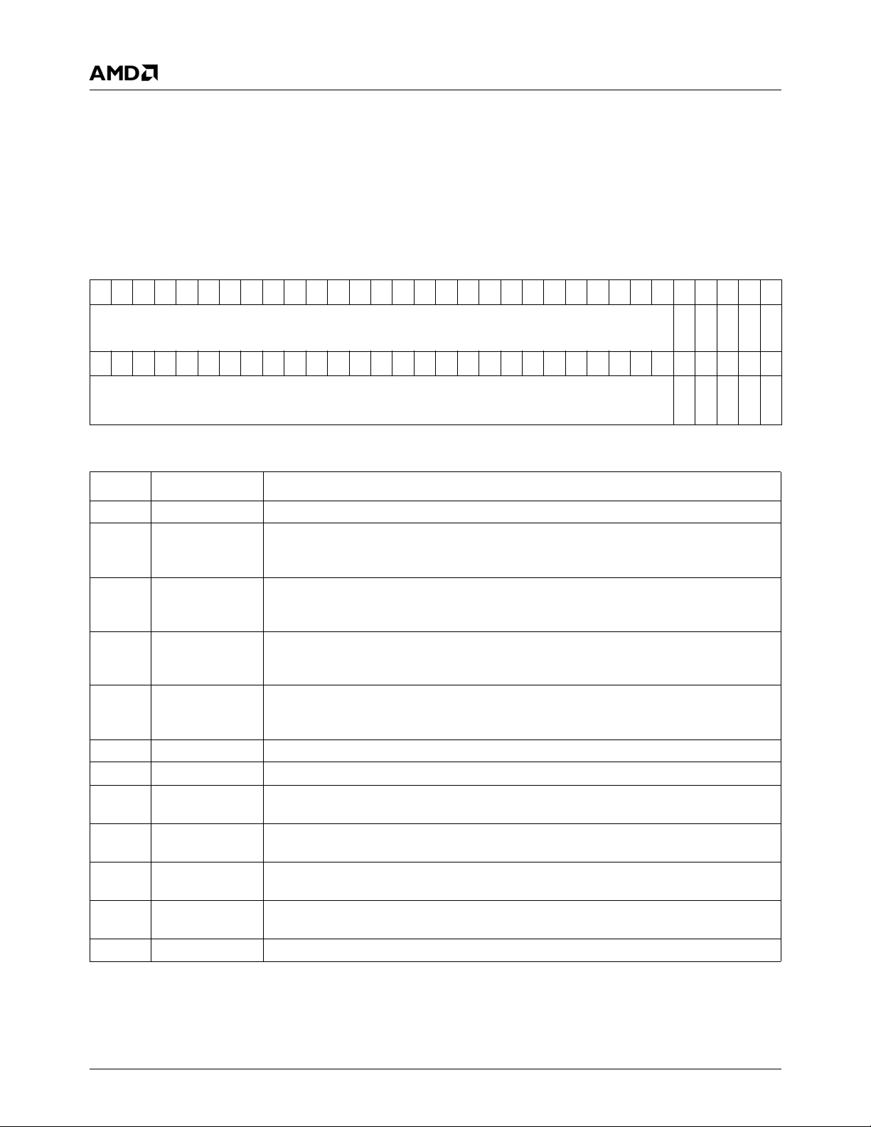
33234H
GLIU Register Descriptions
4.2.1.3 GLD SMI MSR (GLD_MSR_SMI)
MSR Address GLIU0: 10002002h
GLIU1: 40002002h
Ty p e R / W
Reset Value 00000000_00000001h
The flags are set with internal conditions. The internal conditions are always capable of setting the flag, but if the mask is 1,
the flagged condition will not trigger the SMI signal. Reads to the flags return the value. Write = 1 to the flag, clears the
value. Write = 0 has no effect on the flag.
_MSR_SMI Register Map
GLD
63 62 61 60 59 58 57 56 55 54 53 52 51 50 49 48 47 46 45 44 43 42 41 40 39 38 37 36 35 34 33 32
RSVD
SFLAG4
SFLAG3
SFLAG2
SFLAG1
31 30 29 28 27 26 25 24 23 22 21 20 19 18 17 16 15 14 13 12 11 10 9 8 7 6 5 4 3 2 1 0
RSVD
SMASK4
SMASK3
SMASK2
SMASK1
GLD_MSR_SMI Bit Descriptions
SFLAG0
SMASK0
Bit Name Description
63:37 RSVD Reserved.
36 SFLAG4 SMI Flag4. If high, records that an SMI was generated due to a Statistic Counter 3
(GLIU0 MSR 100000ACh, GLIU1 MSR 400000ACh) event. Write 1 to clear; writing 0 has
no effect. SMASK4 (bit 4) must be low to generate SMI and set flag.
35 SFLAG3 SMI Flag3. If high, records that an SMI was generated due to a Statistic Counter 2
(GLIU0 MSR 100000A8h, GLIU1 MSR 400000A8h) event. Write 1 to clear; writing 0 has
no effect. SMASK3 (bit 3) must be low to generate SMI and set flag.
34 SFLAG2 SMI Flag2. If high, records that an SMI was generated due to a Statistic Counter 1
(GLIU0 MSR 100000A4h, GLIU1 MSR 400000A4h) event. Write 1 to clear; writing 0 has
no effect. SMASK2 (bit 2) must be low to generate SMI and set flag.
33 SFLAG1 SMI Flag1. If high, records that an SMI was generated due to a Statistic Counter 0
(GLIU0 MSR 100000A0h, GLIU1 MSR 400000A0h) event. Write 1 to clear; writing 0 has
no effect. SMASK1 (bit 1) must be low to generate SMI and set flag.
32 SFLAG0 SMI Flag0. Unexpected Type (HW Emulation).
31:5 RSVD Reserved.
4 SMASK4 SMI Mask4. Write 0 to enable SFLAG4 (bit 37) and to allow a Statistic Counter 3 (GLIU0
MSR 100000ACh, GLIU1 MSR 400000ACh) event to generate an SMI.
3 SMASK3 SMI Mask3. Write 0 to enable SFLAG3 (bit 36) and to allow a Statistic Counter 2 (GLIU0
MSR 100000A8h, GLIU1 MSR 400000A8h) event to generate an SMI.
2 SMASK2 SMI Mask2. Write 0 to enable SFLAG2 (bit 34) and to allow a Statistic Counter 1 (GLIU0
MSR 100000A4h, GLIU1 MSR 400000A4h) event to generate an SMI.
1 SMASK1 SMI Mask1. Write 0 to enable SFLAG1 (bit 33) and to allow a Statistic Counter 0 (GLIU0
MSR 100000A0h, GLIU1 MSR 400000A0h) event to generate an SMI.
0 SMASK0 SMI Mask0. Unexpected Type (HW Emulation).
56 AMD Geode™ LX Processors Data Book
Page 57

GLIU Register Descriptions
33234H
4.2.1.4 GLD Error MSR (GLD_MSR_ERROR)
MSR Address GLIU0: 10002003h
GLIU1: 40002003h
Ty p e R / W
Reset Value 00000000_00000000h
The flags are set with internal conditions. The internal conditions are always capable of setting the flag, but if the mask is 1,
the flagged condition will not trigger the ERR signal. Reads to the flags return the value. Write = 1 to the flag, clears the
value. Write = 0 has no effect on the flag.
_MSR_ERROR Register Map
GLD
63 62 61 60 59 58 57 56 55 54 53 52 51 50 49 48 47 46 45 44 43 42 41 40 39 38 37 36 35 34 33 32
RSVD
EFLAG9
EFLAG8
EFLAG7
EFLAG6
EFLAG5
EFLAG4
EFLAG3
EFLAG2
EMASK2
EFLAG1
EMASK1
EFLAG14
EFLAG13
EFLAG12
EFLAG11
EFLAG10
313029282726252423222120191817161514131211109876543210
RSVD
EMASK9
EMASK8
EMASK7
EMASK6
EMASK5
EMASK4
EMASK14
EMASK13
EMASK12
EMASK11
EMASK10
EMASK3
GLD_MSR_ERROR Bit Descriptions
EFLAG0
EMASK0
Bit Name Description
63:47 RSVD Reserved.
46 EFLAG14 Data Comparator Error Flag 3. If high, records that an ERR was generated due to a
Data Comparator 3 (DA_COMPARE_VAL_LO3/DA_COMPARE_VAL_HI3, GLIU0 MSR
100000DCh/100000DDh, GLIU1 MSR 400000DCh/400000DDh) event. Write 1 to clear;
writing 0 has no effect. EMASK14 (bit 14) must be low to generate ERR and set flag.
45 EFLAG13 Data Comparator Error Flag 2. If high, records that an ERR was generated due to a
Data Comparator 2 (DA_COMPARE_VAL_LO2/DA_COMPARE_VAL_HI2, GLIU0 MSR
100000D8h/100000D9h, GLIU1 MSR 400000D8h/400000D9h) event. Write 1 to clear;
writing 0 has no effect. EMASK13 (bit 13) must be low to generate ERR and set flag.
44 EFLAG12 Data Comparator Error Flag 1. If high, records that an ERR was generated due to a
Data Comparator 1 (DA_COMPARE_VAL_LO1/DA_COMPARE_VAL_HI1, GLIU0 MSR
100000D4h/100000D5h, GLIU1 MSR 400000D4h/400000D5h) event. Write 1 to clear;
writing 0 has no effect. EMASK12 (bit 12) must be low to generate ERR and set flag.
43 EFLAG11 Data Comparator Error Flag 0. If high, records that an ERR was generated due to a
Data Comparator 0 (DA_COMPARE_VAL_LO0/DA_COMPARE_VAL_HI0, GLIU0 MSR
100000D0h/100000D1h, GLIU1 MSR 400000D0h/400000D1h) event. Write 1 to clear;
writing 0 has no effect. EMASK11(bit 11) must be low to generate ERR and set flag.
42 EFLAG10 Request Comparator Error Flag 3. If high, records that an ERR was generated due to a
Request Comparator 3 (RQ_COMPARE_VAL3, GLIU0 MSR 100000C6h, GLIU1 MSR
400000C6h) event. Write 1 to clear; writing 0 has no effect. EMASK10 (bit 10) must be
low to generate ERR and set flag.
41 EFLAG9 Request Comparator Error Flag 2. If high, records that an ERR was generated due to a
Request Comparator 2 (RQ_COMPARE_VAL2, GLIU0 MSR 100000C4h, GLIU1 MSR
400000C4h) event. Write 1 to clear; writing 0 has no effect. EMASK9 (bit 9) must be low
to generate ERR and set flag.
40 EFLAG8 Request Comparator Error Flag 1. If high, records that an ERR was generated due to a
Request Comparator 1 (RQ_COMPARE_VAL1, GLIU0 MSR 100000C2h, GLIU1 MSR
400000C2h) event. Write 1 to clear; writing 0 has no effect. EMASK8 (bit 8) must be low
to generate ERR and set flag.
AMD Geode™ LX Processors Data Book 57
Page 58

33234H
_MSR_ERROR Bit Descriptions (Continued)
GLD
GLIU Register Descriptions
Bit Name Description
39 EFLAG7 Request Comparator Error Flag 0. If high, records that an ERR was generated due to a
Request Comparator 0 (RQ_COMPARE_VAL0, GLIU0 MSR 100000C0h, GLIU1 MSR
400000C0h) event. Write 1 to clear; writing 0 has no effect. EMASK7 (bit 7) must be low
to generate ERR and set flag.
38 EFLAG6 Statistic Counter Error Flag 3. If high, records that an ERR was generated due to a
Statistic Counter 3 (GLIU0 MSR 100000ACh, GLIU1 MSR 400000ACh) event. Write 1 to
clear; writing 0 has no effect. EMASK6 (bit 6) must be low to generate ERR and set flag.
37 EFLAG5 Statistic Counter Error Flag 2. If high, records that an ERR was generated due to a
Statistic Counter 2 (GLIU0 MSR 100000A8h, GLIU1 MSR 400000A8h) event. Write 1 to
clear; writing 0 has no effect. EMASK5 (bit 5) must be low to generate ERR and set flag.
36 EFLAG4 Statistic Counter Error Flag 1. If high, records that an ERR was generated due to a
Statistic Counter 1 (GLIU0 MSR 100000A4h, GLIU1 MSR 400000A4h) event. Write 1 to
clear; writing 0 has no effect. EMASK4 (bit 4) must be low to generate ERR and set flag.
35 EFLAG3 Statistic Counter Error Flag 0. If high, records that an ERR was generated due to a
Statistic Counter 0 (GLIU0 MSR 100000A0h, GLIU1 MSR 400000A0h) event. Write 1 to
clear; writing 0 has no effect. EMASK3 (bit 3) must be low to generate ERR and set flag.
34 EFLAG2 Unhandled SMI Error Flag. If high, records that an ERR was generated due an unhan-
dled SSMI (synchronous error). Write 1 to clear; writing 0 has no effect. EMASK2 (bit 2)
must be low to generate ERR and set flag Unhandled SMI.
33 EFLAG1 Unexpected Address Error Flag. If high, records that an ERR was generated due an
unexpected address (synchronous error). Write 1 to clear; writing 0 has no effect.
EMASK1 (bit 1) must be low to generate ERR and set flag.
32 EFLAG0 Unexpected Type Error Flag. If high, records that an ERR was generated due an unex-
pected type (synchronous error). Write 1 to clear; writing 0 has no effect. EMASK0 (bit 0)
must be low to generate ERR and set flag.
31:15 RSVD Reserved.
14 EMASK14 Data Comparator Error Mask 3. Write 0 to enable EFLAG14 (bit 46) and to allow a Data
Comparator 3 (DA_COMPARE_VAL_LO3/DA_COMPARE_VAL_HI3, GLIU0 MSR
100000DCh/100000DDh, GLIU1 MSR 400000DCh/400000DDh) event to generate an
ERR and set flag.
13 EMASK13 Data Comparator Error Mask 2. Write 0 to enable EFLAG13 (bit 45) and to allow a Data
Comparator 2 (DA_COMPARE_VAL_LO2/DA_COMPARE_VAL_HI2, GLIU0 MSR
100000D8h/100000D9h, GLIU1 MSR 400000D8h/400000D9h) event to generate an
ERR and set flag.
12 EMASK12 Data Comparator Error Mask 1. Write 0 to enable EFLAG12 (bit 44) and to allow a Data
Comparator 1 (DA_COMPARE_VAL_LO1/DA_COMPARE_VAL_HI1, GLIU0 MSR
100000D4h/100000D5h, GLIU1 MSR 400000D4h/400000D5h) event to generate an
ERR and set flag.
11 EMASK11 Data Comparator Error Mask 0. Write 0 to enable EFLAG11 (bit 43) and to allow a Data
Comparator 0 (DA_COMPARE_VAL_LO0/DA_COMPARE_VAL_HI0, GLIU0 MSR
100000D4h/100000D5h, GLIU1 MSR 400000D4h/400000D5h) event to generate an
ERR and set flag.
10 EMASK10 Request Comparator Error Mask 3. Write 0 to enable EFLAG10 (bit 42) and to allow a
Request Comparator 3 (RQ_COMPARE_VAL3, GLIU0 MSR 100000C6h, GLIU1 MSR
400000C6h) event to generate an ERR
9 EMASK9 Request Comparator Error Mask 2. Write 0 to enable EFLAG9 (bit 41) and to allow a
Request Comparator 2 (RQ_COMPARE_VAL2, GLIU0 MSR 100000C4h, GLIU1 MSR
400000C4h) event to generate an ERR.
58 AMD Geode™ LX Processors Data Book
Page 59
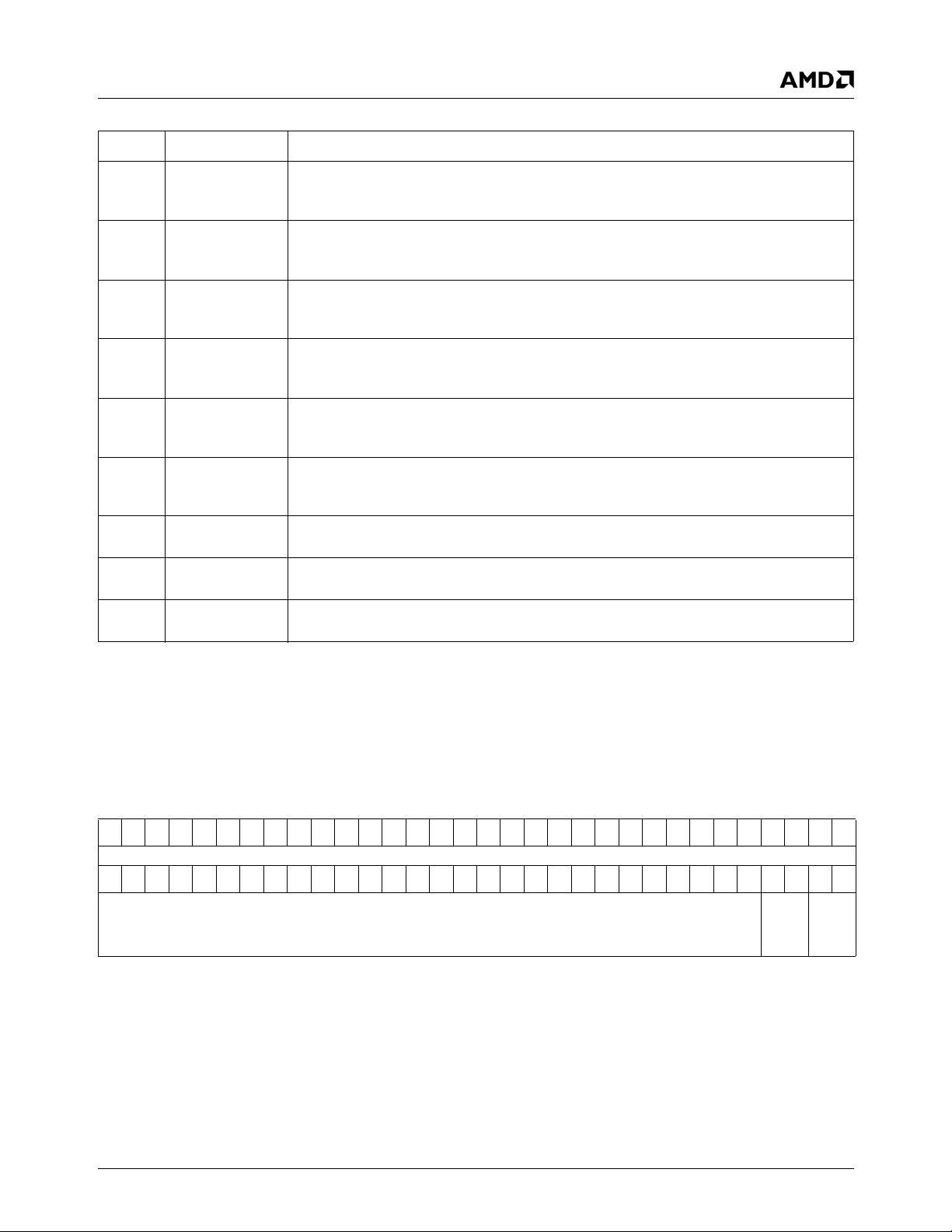
GLIU Register Descriptions
_MSR_ERROR Bit Descriptions (Continued)
GLD
33234H
Bit Name Description
8 EMASK8 Request Comparator Error Mask 1. Write 0 to enable EFLAG8 (bit 40) and to allow a
Request Comparator 1 (RQ_COMPARE_VAL1, GLIU0 MSR 100000C2h, GLIU1 MSR
400000C2h) event to generate an ERR
7 EMASK7 Request Comparator Error Mask 0. Write 0 to enable EFLAG7 (bit 39) and to allow a
Request Comparator 0 (RQ_COMPARE_VAL0, GLIU0 MSR 100000C0h, GLIU1 MSR
400000C0h) event to generate an ERR
6 EMASK6 Statistic Counter Error Mask 3. Write 0 to enable EFLAG6 (bit 38) and to allow a Statis-
tic Counter 3 (GLIU0 MSR 100000ACh, GLIU1 MSR 400000ACh) event to generate an
ERR.
5 EMASK5 Statistic Counter Error Mask 2. Write 0 to enable EFLAG5 (bit 37) and to allow a Statis-
tic Counter 2 (GLIU0 MSR 100000A8h, GLIU1 MSR 400000A8h) event to generate an
ERR.
4 EMASK4 Statistic Counter Error Mask 1. Write 0 to enable EFLAG4 (bit 36) and to allow a Statis-
tic Counter 1 (GLIU0 MSR 100000A4h, GLIU1 MSR 400000A4h) event to generate an
ERR.
3 EMASK3 Statistic Counter Error Mask 0. Write 0 to enable EFLAG3 (bit 35) and to allow a Statis-
tic Counter 0 (GLIU0 MSR 100000A0h, GLIU1 MSR 400000A0h) event to generate an
ERR.
2 EMASK2 Unhandled SMI Error Mask 2. Write 0 to enable EFLAG2 (bit 34) and to allow the
unhandled SSMI (synchronous error) event to generate an ERR.
1 EMASK1 Unexpected Address Error Mask 1. as Write 0 to enable EFLAG1 (bit 33) and to allow
the unexpected address (synchronous error) event to generate an ERR.
0 EMASK0 Unexpected Type Error Mask 0. Write 0 to enable EFLAG0 (bit 32) and to allow the
unexpected type (synchronous error) event to generate an ERR.
4.2.1.5 GLD Power Management MSR (GLD_MSR_PM)
MSR Address GLIU0: 10002004h
GLIU1: 40002004h
Ty p e R / W
Reset Value 00000000_00000000h
GLD_MSR_PM Register Map
63 62 61 60 59 58 57 56 55 54 53 52 51 50 49 48 47 46 45 44 43 42 41 40 39 38 37 36 35 34 33 32
RSVD
313029282726252423222120191817161514131211109876543210
RSVD
PMODE_1
PMODE_0
AMD Geode™ LX Processors Data Book 59
Page 60

33234H
_MSR_PM Bit Descriptions
GLD
Bit Name Description
63:4 RSVD Reserved.
3:2 PMODE_1 Power Mode 1. Statistics and Time Slice Counters.
00: Disable clock gating. Clocks are always on.
01: Enable hardware clock gating. Clock goes off whenever this module’s circuits are not
busy.
10, 11: Reserved.
1:0 PMODE_0 Power Mode 0. Online GLIU logic.
00: Disable clock gating. Clocks are always on.
01: Enable hardware clock gating. Clock goes off whenever this module’s circuits are not
busy.
10, 11: Reserved.
4.2.1.6 GLD Diagnostic MSR (GLD_MSR_DIAG)
MSR Address GLIU0: 10002005h
GLIU1: 40002005h
Ty p e R / W
Reset Value 00000000_00000000h
GLIU Register Descriptions
This register is reserved for internal use by AMD and should not be written to.
4.2.2 GLIU Specific Registers
4.2.2.1 Coherency (COH)
MSR Address GLIU0: 10000080h
GLIU1: 40000080h
Ty p e R / W
Reset Value Configuration Dependent
COH Register Map
63 62 61 60 59 58 57 56 55 54 53 52 51 50 49 48 47 46 45 44 43 42 41 40 39 38 37 36 35 34 33 32
RSVD
313029282726252423222120191817161514131211109876543210
RSVD COHP
COH Bit Descriptions
Bit Name Description
63:3 RSVD Reserved.
2:0 COHP Coherent Device Port. The port that coherents snoops are routed to. If the coherent
device is on the other side of a bridge, the COHP points to the bridge.
60 AMD Geode™ LX Processors Data Book
Page 61

GLIU Register Descriptions
33234H
4.2.2.2 Port Active Enable (PAE)
MSR Address GLIU0: 10000081h
GLIU1: 40000081h
Ty p e R / W
Reset Value Boot Strap Dependent
Ports that are not implemented return 00 (RSVD). Ports that are slave only return 11. Master/Slave ports return the values
as stated.
GLIU0 will reset all PAE to 11 (ON) except that GLIU0 PAE3 resets to 00 when the debug stall bootstrap is active (CPU port
resets inactive for debug stall).
PAE Register Map
63 62 61 60 59 58 57 56 55 54 53 52 51 50 49 48 47 46 45 44 43 42 41 40 39 38 37 36 35 34 33 32
RSVD
313029282726252423222120191817161514131211109876543210
RSVD PAE0 PAE7 PAE6 PAE5 PAE4 PAE3 PAE2 PAE1
PAE Bit Descriptions
Bit Name Description
63:16 RSVD Reserved.
15:14 PAE0 Port Active Enable for Port 0. (GLIU0 = GLIU; GLIU1 = GLIU.)
00: OFF - Master transactions are disabled.
01: LOW - Master transactions limited to 1 outstanding transaction.
10: Reserved.
11: ON - Master transactions enabled with no limitations.
13:12 PAE7 Port Active Enable for Port 7. (GLIU0 = Not Used; GLIU1 = Not Used.)
See bits [15:14] for decode.
11:10 PAE6 Port Active Enable for Port 6. (GLIU0 = Not Used; GLIU1 = SB.)
See bits [15:14] for decode.
9:8 PAE5 Port Active Enable for Port 5. (GLIU0 = GP; GLIU1 = VIP.)
See bits [15:14] for decode.
7:6 PAE4 Port Active Enable for Port 4. (GLIU0 = DC; GLIU1 = GLPCI.)
See bits [15:14] for decode.
5:4 PAE3 Port Active Enable for Port 3. (GLIU0 = CPU Core; GLIU1 = GLCP.)
See bits [15:14] for decode.
3:2 PAE2 Port Active Enable for Port 2. (GLIU0 = Interface to GLIU1; GLIU1 = VP.)
See bits [15:14] for decode.
1:0 PAE1 Port Active Enable for Port 1. (GLIU0 = GLMC; GLIU1 = Interface to GLIU0.)
See bits [15:14] for decode.
AMD Geode™ LX Processors Data Book 61
Page 62

33234H
GLIU Register Descriptions
4.2.2.3 Arbitration (ARB)
MSR Address GLIU0: 10000082h
GLIU1: 40000082h
Ty p e R / W
Reset Value 10000000_00000000h
ARB Register Map
63 62 61 60 59 58 57 56 55 54 53 52 51 50 49 48 47 46 45 44 43 42 41 40 39 38 37 36 35 34 33 32
RSVD
RSVD
QUACK_EN
PIPE_DIS
DACK_EN
313029282726252423222120191817161514131211109876543210
RSVD
ARB Bit Descriptions
Bit Name Description
63 QUACK_EN Quadruple Acknowledge Enabled. Allow four acknowledgements in a row before
advancing round-robin arbitration. Only applies when arbitrating matching priorities.
0: Disable.
1: Enable.
62 PIPE_DIS Pipelined Arbitration Disabled.
0: Pipelined arbitration enabled and GLIU is not limited to one outstanding transaction.
1: Limit the entire GLIU to one outstanding transaction.
61 RSVD Reserved.
60 DACK_EN Double Acknowledge Enabled. Allow two acknowledgements in a row before advanc-
ing round-robin arbitration. Only applies when arbitrating matching priorities.
0: Disable.
1: Enable.
59:0 RSVD Reserved.
4.2.2.4 Asynchronous SMI (ASMI)
MSR Address GLIU0: 10000083h
GLIU1: 40000083h
Ty p e R / W
Reset Value 00000000_00000000h
ASMI is a condensed version of the port ASMI signals. The MASK bits can be used to prevent a device from issuing an
ASMI. If the MASK = 1, the device’s ASMI is disabled.
ASMI Register Map
63 62 61 60 59 58 57 56 55 54 53 52 51 50 49 48 47 46 45 44 43 42 41 40 39 38 37 36 35 34 33 32
RSVD
31 30 29 28 27 26 25 24 23 22 21 20 19 18 17 16 15 14 13 12 11 10 9 8 7 6 5 4 3 2 1 0
RSVD
ASMI_FLAG7
ASMI_FLAG6
ASMI_FLAG5
ASMI_FLAG4
ASMI_FLAG3
ASMI_FLAG2
ASMI_MASK7
ASMI_MASK6
ASMI_MASK5
ASMI_MASK4
ASMI_MASK3
ASMI_MASK2
ASMI_MASK1
ASMI_MASK0
62 AMD Geode™ LX Processors Data Book
ASMI_FLAG1
ASMI_FLAG0
Page 63

GLIU Register Descriptions
33234H
ASMI Bit Descriptions
Bit Name Description
63:16 RSVD Reserved.
15 ASMI_MASK7 Asynchronous SMI Mask for Port 7. (GLIU0 = Not Used; GLIU1 = Not Used.) Write 0 to
allow Port 7 to generate an ASMI. ASMI status is reported in bit 7.
14 ASMI_MASK6 Asynchronous SMI Mask for Port 6. (GLIU0 = Not Used; GLIU1 = SB.) Write 0 to allow
Port 6 to generate an ASMI. ASMI status is reported in bit 6.
13 ASMI_MASK5 Asynchronous SMI Mask for Port 5. (GLIU0 = GP; GLIU1 = VIP.) Write 0 to allow Port 5
to generate an ASMI. ASMI status is reported in bit 5.
12 ASMI_MASK4 Asynchronous SMI Mask for Port 4. (GLIU0 = DC; GLIU1 = GLPCI.) Write 0 to allow
Port 4 to generate an ASMI. ASMI status is reported in bit 4.
11 ASMI_MASK3 Asynchronous SMI Mask for Port 3. (GLIU0 = CPU Core; GLIU1 = GLCP.) Write 0 to
allow Port 3 to generate an ASMI. ASMI status is reported in bit 3.
10 ASMI_MASK2 Asynchronous SMI Mask for Port 2. (GLIU0 = Interface to GLIU1; GLIU1 = VP.) Write 0
to allow Port 2 to generate an ASMI. ASMI status is reported in bit 2.
9 ASMI_MASK1 Asynchronous SMI Mask for Port 1. (GLIU0 = GLMC; GLIU1 = Interface to GLIU0.)
Write 0 to allow Port 1 to generate an ASMI. ASMI status is reported in bit 1.
8 ASMI_MASK0 Asynchronous SMI Mask for Port 0. (GLIU0 = GLIU; GLIU1 = GLIU.) Write 0 to allow
Port 0 to generate an ASMI. ASMI status is reported in bit 0.
7 ASMI_FLAG7
(RO)
6 ASMI_FLAG6
(RO)
5 ASMI_FLAG5
(RO)
4 ASMI_FLAG4
(RO)
3 ASMI_FLAG3
(RO)
2 ASMI_FLAG2
(RO)
1 ASMI_FLAG1
(RO)
0 ASMI_FLAG0
(RO)
Asynchronous SMI Flag for Port 7 (Read Only). (GLIU0 = Not Used; GLIU1 = Not
Used.). If 1, this bit indicates that an ASMI was generated by Port 7. Cleared by source.
Asynchronous SMI Flag for Port 6 (Read Only). (GLIU0 = Not Used; GLIU1 = SB.) If 1,
this bit indicates that an ASMI was generated by Port 6. Cleared by source.
Asynchronous SMI Flag for Port 5 (Read Only). (GLIU0 = GP; GLIU1 = VIP.) If 1, this
bit indicates that an ASMI was generated by Port 5. Cleared by source.
Asynchronous SMI Flag for Port 4 (Read Only). (GLIU0 = DC; GLIU1 = GLPCI.) If 1,
this bit indicates that an ASMI was generated by Port 4. Cleared by source.
Asynchronous SMI Flag for Port 3 (Read Only). (GLIU0 = CPU Core; GLIU1 = GLCP.)
If 1, this bit indicates that an ASMI was generated by Port37. Cleared by source.
Asynchronous SMI Flag for Port 2 (Read Only). (GLIU0 = Interface to GLIU1; GLIU1 =
VP.) If 1, this bit indicates that an ASMI was generated by Port 2. Cleared by source.
Asynchronous SMI Flag for Port 1 (Read Only). (GLIU0 = GLMC; GLIU1 = Interface to
GLIU0.) If 1, this bit indicates that an ASMI was generated by Port 1. Cleared by source.
Asynchronous SMI Flag for Port 0 (Read Only). (GLIU0 = GLIU; GLIU1 = GLIU.) If 1,
this bit indicates that an ASMI was generated by Port 0. Cleared by source.
4.2.2.5 Asynchronous ERR (AERR)
MSR Address GLIU0: 10000084h
GLIU1: 40000084h
Ty p e R / W
Reset Value 00000000_00000000h
AERR is a condensed version of the port ERR signals. The MASK bits can be used to prevent a device from issuing an
AERR. If the MASK = 1, the device’s AERR is disabled.
AMD Geode™ LX Processors Data Book 63
Page 64

33234H
GLIU Register Descriptions
AERR Register Map
63 62 61 60 59 58 57 56 55 54 53 52 51 50 49 48 47 46 45 44 43 42 41 40 39 38 37 36 35 34 33 32
RSVD
313029282726252423222120191817161514131211109876543210
RSVD
AERR7
AERR6
AERR5
AERR4
AERR3
AERR2
AERR1
AERR0
AERR_MASK7
AERR_MASK6
AERR_MASK5
AERR_MASK4
AERR_MASK3
AERR_MASK2
AERR_MASK1
AERR_MASK0
AERR Bit Descriptions
Bit Name Description
63:16 RSVD Reserved.
15 AERR_MASK7 Asynchronous Error Mask for Port 7. (GLIU0 = Not Used; GLIU1 = Not Used.) Write 0
to allow Port 7 to generate an AERR. AERR status is reported in bit 7.
14 AERR_MASK6 Asynchronous Error Mask for Port 6. (GLIU0 = Not Used; GLIU1 = SB.) Write 0 to
allow Port 6 to generate an AERR. AERR status is reported in bit 6.
13 AERR_MASK5 Asynchronous Error Mask for Port 5. (GLIU0 = GP; GLIU1 = VIP.) Write 0 to allow Port
5 to generate an AERR. AERR status is reported in bit 5.
12 AERR_MASK4 Asynchronous Error Mask for Port 4. (GLIU0 = DC; GLIU1 = GLPCI.) Write 0 to allow
Port 4 to generate an AERR. AERR status is reported in bit 4.
11 AERR_MASK3 Asynchronous Error Mask for Port 3. (GLIU0 = CPU Core; GLIU1 = GLCP.) Write 0 to
allow Port 3 to generate an AERR. AERR status is reported in bit 3.
10 AERR_MASK2 Asynchronous Error Mask for Port 2. (GLIU0 = Interface to GLIU1; GLIU1 = VP.) Write
0 to allow Port 2 to generate an AERR. AERR status is reported in bit 2.
9 AERR_MASK1 Asynchronous Error Mask for Port 1. (GLIU0 = GLMC; GLIU1 = Interface to GLIU0.)
Write 0 to allow Port 1 to generate an AERR. AERR status is reported in bit 1.
8 AERR_MASK0 Asynchronous Error Mask for Port 0. (GLIU0 = GLIU; GLIU1 = GLIU.) Write 0 to allow
Port 0 to generate an AERR. AERR status is reported in bit 0.
7 AERR_FLAG7
(RO)
6 AERR_FLAG6
(RO)
5 AERR_FLAG5
(RO)
4 AERR_FLAG4
(RO)
3 AERR_FLAG3
(RO)
2 AERR_FLAG2
(RO)
1 AERR_FLAG1
(RO)
0 AERR_FLAG0
(RO)
Asynchronous Error for Port 7 (Read Only). (GLIU0 = Not Used; GLIU1 = Not Used.) If
1, indicates that an AERR was generated by Port 7. Cleared by source.
Asynchronous Error for Port 6 (Read Only). (GLIU0 = Not Used; GLIU1 = SB.) If 1,
indicates that an AERR was generated by Port 6. Cleared by source.
Asynchronous Error for Port 5 (Read Only). (GLIU0 = GP; GLIU1 = VIP.) If 1, indicates
that an AERR was generated by Port 5. Cleared by source.
Asynchronous Error for Port 4 (Read Only). (GLIU0 = DC; GLIU1 = GLPCI.) If 1, indicates that an AERR was generated by Port 4. Cleared by source.
Asynchronous Error for Port 3 (Read Only). (GLIU0 = CPU Core; GLIU1 = GLCP.) If 1,
indicates that an AERR was generated by Port 3. Cleared by source.
Asynchronous Error for Port 2 (Read Only). (GLIU0 = Interface to GLIU1; GLIU1 =
VP.) If 1, indicates that an AERR was generated by Port 2. Cleared by source.
Asynchronous Error for Port 1 (Read Only). (GLIU0 = GLMC; GLIU1 = Interface to
GLIU0.) If 1, indicates that an AERR was generated by Port 1. Cleared by source.
Asynchronous Error for Port 0 (Read Only). (GLIU0 = GLIU; GLIU1 = GLIU.) If 1, indicates that an AERR was generated by Port 0. Cleared by source.
64 AMD Geode™ LX Processors Data Book
Page 65

GLIU Register Descriptions
33234H
4.2.2.6 GLIU Physical Capabilities (PHY_CAP)
MSR Address GLIU0: 10000086h
GLIU1: 40000086h
Ty p e R / W
Reset Value GLIU0: 20291830_010C1086h
GLIU1: 20311030_0100400Ah
PHY_CAP Register Map
63 62 61 60 59 58 57 56 55 54 53 52 51 50 49 48 47 46 45 44 43 42 41 40 39 38 37 36 35 34 33 32
NPORTS NCOH NIOD_SC NIOD_BM NP2D_BMK
RSVD
NSTAT_CNT
31 30 29 28 27 26 25 24 23 22 21 20 19 18 17 16 15 14 13 12 11 10 9 8 7 6 5 4 3 2 1 0
NP2D_BMK
NDBG_DA_CMP
NP2D_SC NP2D_RO NP2D_R NP2D_BMO NP2D_BM
NDBG_RQ_CMP
PHY_CAP Bit Descriptions
Bit Name Description
63 RSVD Reserved.
62:60 NSTAT_CNT Number Of Statistic Counters.
59:57 NDBG_DA_CMP Number Of Data Comparators.
56:54 NDBG_RQ_CMP Number Of Request Comparators.
53:51 NPORTS Number of Ports on the GLIU.
50:48 NCOH Number of Coherent Devices.
47:42 NIOD_SC Number of IOD_SC Descriptors.
41:36 NIOD_BM Number of IOD_BM Descriptors.
35:30 NP2D_BMK Number of P2D_BMK Descriptors.
29:24 NP2D_SC Number of P2D_SC Descriptors.
23:18 NP2D_RO Number of P2D_RO Descriptors.
17:12 NP2D_R Number of P2D_R Descriptors.
11:6 NP2D_BMO Number of P2D_BMO Descriptors.
5:0 NP2D_BM Number of P2D_BM Descriptors.
AMD Geode™ LX Processors Data Book 65
Page 66

33234H
GLIU Register Descriptions
4.2.2.7 N Outstanding Response (NOUT_RESP)
MSR Address GLIU0: 10000087h
GLIU1: 40000087h
Ty p e R O
Reset Value 00000000_00000000h
NOUT_RESP Register Map
63 62 61 60 59 58 57 56 55 54 53 52 51 50 49 48 47 46 45 44 43 42 41 40 39 38 37 36 35 34 33 32
NOUT_RESP7 NOUT_RESP6 NOUT_RESP5 NOUT_RESP4
31 30 29 28 27 26 25 24 23 22 21 20 19 18 17 16 15 14 13 12 11 10 9 8 7 6 5 4 3 2 1 0
NOUT_RESP3 NOUT_RESP2 NOUT_RESP1 NOUT_RESP9
NOUT_RESP Bit Descriptions
Bit Name Description
63:56 NOOUT_RESP7 Number of Outstanding Responses on Port 7. (GLIU0 = Not Used; GLIU1 = Not
Used.)
55:48 NOOUT_RESP6 Number of Outstanding Responses on Port 6. (GLIU0 = Not Used; GLIU1 = SB.)
47:40 NOOUT_RESP5 Number of Outstanding Responses on Port 5. (GLIU0 = GP; GLIU1 = VIP.)
39:32 NOOUT_RESP4 Number of Outstanding Responses on Port 4. (GLIU0 = DC; GLIU1 = GLPCI.)
31:24 NOOUT_RESP3 Number of Outstanding Responses on Port 3. (GLIU0 = CPU Core; GLIU1 = GLCP.)
23:16 NOOUT_RESP2 Number of Outstanding Responses on Port 2. (GLIU0 = Interface to GLIU1; GLIU1 =
VP.)
15:8 NOOUT_RESP1 Number of Outstanding Responses on Port 1. (GLIU0 = GLMC; GLIU1 = Interface to
GLIU0.)
7:0 NOOUT_RESP0 Number of Outstanding Responses on Port 0. (GLIU0 = GLIU; GLIU1 = GLIU.)
66 AMD Geode™ LX Processors Data Book
Page 67

GLIU Register Descriptions
33234H
4.2.2.8 N Outstanding Write Data (NOUT_WDATA)
MSR Address GLIU0: 10000088h
GLIU1: 40000088h
Ty p e R O
Reset Value 00000000_00000000h
NOUT_WDATA Register Map
63 62 61 60 59 58 57 56 55 54 53 52 51 50 49 48 47 46 45 44 43 42 41 40 39 38 37 36 35 34 33 32
NOUT_WDATA7 NOUT_WDATA6 NOUT_WDATA5 NOUT_WDATA4
313029282726252423222120191817161514131211109876543210
NOUT_WDATA3 NOUT_WDATA2 NOUT_WDATA1 NOUT_WDATA0
NOUT_WDATA Bit Descriptions
Bit Name Description
63:56 NOOUT_WDATA7 Number of Outstanding Write Data on Port 7. (GLIU0 = Not Used; GLIU1 = Not
Used.)
55:48 NOOUT_WDATA6 Number of Outstanding Write Data on Port 6. (GLIU0 = Not Used; GLIU1 = SB.)
47:40 NOOUT_WDATA5 Number of Outstanding Write Data on Port 5. (GLIU0 = GP; GLIU1 = VIP.)
39:32 NOOUT_WDATA4 Number of Outstanding Write Data on Port 4. (GLIU0 = DC; GLIU1 = GLPCI.)
31:24 NOOUT_WDATA3 Number of Outstanding Write Data on Port 3. (GLIU0 = CPU Core; GLIU1 =
GLCP.)
23:16 NOOUT_WDATA2 Number of Outstanding Write Data on Port 2. (GLIU0 = Interface to GLIU1; GLIU1
= VP.)
15:8 NOOUT_WDATA1 Number of Outstanding Write Data on Port 1. (GLIU0 = GLMC; GLIU1 = Interface
to GLIU0.)
7:0 NOOUT_WDATA0 Number of Outstanding Write Data on Port 0. (GLIU0 = GLIU; GLIU1 = GLIU.)
4.2.2.9 SLAVE_ONLY
MSR Address GLIU0: 10000089h
GLIU1: 40000089h
Ty p e R O
Reset Value GLIU0: 00000000_00000010h
GLIU1: 00000000_00000100h
SLAVE_ONLY Register Map
63 62 61 60 59 58 57 56 55 54 53 52 51 50 49 48 47 46 45 44 43 42 41 40 39 38 37 36 35 34 33 32
RSVD
31 30 29 28 27 26 25 24 23 22 21 20 19 18 17 16 15 14 13 12 11 10 9 8 7 6 5 4 3 2 1 0
RSVD SLAVE_ONLY
SLAVE_ONLY Bit Descriptions
Bit Name Description
63:8 RSVD Reserved.
7 P7_SLAVE_ONLY Port 7 Slave Only. (GLIU0 = Not Used; GLIU1 = Not Used.) If high, indicates that Port
7 is a slave port. If low, Port 7 is a master/slave port.
AMD Geode™ LX Processors Data Book 67
Page 68

33234H
GLIU Register Descriptions
SLAVE_ONLY Bit Descriptions (Continued)
Bit Name Description
6 P6_SLAVE_ONLY Port 6 Slave Only. (GLIU0 = Not Used; GLIU1 = SB.) If high, indicates that Port 6 is a
slave port. If low, Port 6 is a master/slave port.
5 P5_SLAVE_ONLY Port 5 Slave Only. (GLIU0 = GP; GLIU1 = VIP.) If high, indicates that Port 5 is a slave
port. If low, Port 5 is a master/slave port.
4 P4_SLAVE_ONLY Port 4 Slave Only. (GLIU0 = DC; GLIU1 = GLPCI.) If high, indicates that Port 4 is a
slave port. If low, Port 4 is a master/slave port.
3 P3_SLAVE_ONLY Port 3 Slave Only. (GLIU0 = CPU Core; GLIU1 = GLCP.) If high, indicates that Port 3
is a slave port. If low, Port 3 is a master/slave port.
2 P2_SLAVE_ONLY Port 2 Slave Only. (GLIU0 = Interface to GLIU1; GLIU1 = VP.) If high, indicates that
Port 2 is a slave port. If low, Port 2 is a master/slave port.
1 P1_SLAVE_ONLY Port 1 Slave Only. (GLIU0 = GLMC; GLIU1 = Interface to GLIU0.) If high, indicates
that Port 1 is a slave port. If low, Port 1 is a master/slave port.
0 P0_SLAVE_ONLY Port 0 Slave Only. (GLIU0 = GLIU; GLIU1 = GLIU.) If high, indicates that Port 0 is a
slave port. If low, Port 0 is a master/slave port.
4.2.2.10 WHO AM I (WHOAMI)
MSR Address GLIU0: 1000008Bh
GLIU1: 4000008Bh
Ty p e R O
Reset Value Configuration Dependent
WHO AM I Register Map
63 62 61 60 59 58 57 56 55 54 53 52 51 50 49 48 47 46 45 44 43 42 41 40 39 38 37 36 35 34 33 32
RSVD
31 30 29 28 27 26 25 24 23 22 21 20 19 18 17 16 15 14 13 12 11 10 9 8 7 6 5 4 3 2 1 0
RSVD DSID
WHO AM I Bit Descriptions
Bit Name Description
63:3 RSVD Reserved.
2:0 DSID Source ID of the Initiating Device. Used to prevent self referencing transactions.
000: Port 0 (GLIU0 = GLIU; GLIU1 = GLIU.)
001: Port 1 (GLIU0 = GLMC; GLIU1 = Interface to GLIU0.)
010: Port 2 (GLIU0 = Interface to GLIU1; GLIU1 = VP.)
011: Port 3 (GLIU0 = CPU Core; GLIU1 = GLCP.)
100: Port 4 (GLIU0 = DC; GLIU1 = GLPCI.)
101: Port 5 (GLIU0 = GP; GLIU1 = VIP.)
110: Port 6 (GLIU0 = Not Used; GLIU1 = SB.)
111: Port 7 (GLIU0 = Not Used; GLIU1 = Not Used.)
68 AMD Geode™ LX Processors Data Book
Page 69

GLIU Register Descriptions
33234H
4.2.2.11 GLIU Slave Disable (GLIU_SLV)
MSR Address GLIU0: 1000008Ch
GLIU1: 4000008Ch
Ty p e R / W
Reset Value 00000000_00000000h
The slave disable registers are available for the number of ports on the GLIU. The unused ports return 0.
GLIU_SLV Register Map
63 62 61 60 59 58 57 56 55 54 53 52 51 50 49 48 47 46 45 44 43 42 41 40 39 38 37 36 35 34 33 32
RSVD
31 30 29 28 27 26 25 24 23 22 21 20 19 18 17 16 15 14 13 12 11 10 9 8 7 6 5 4 3 2 1 0
RSVD
SLAVE_DIS7
SLAVE_DIS6
SLAVE_DIS5
SLAVE_DIS4
SLAVE_DIS3
SLAVE_DIS2
SLAVE_DIS1
GLIU_SLV Bit Descriptions
Bit Name Description
SLAVE_DIS0
63:8 RSVD Reserved.
7 SLAVE_DIS7 Slave Transactions Disable for Port 7. (GLIU0 = Not Used; GLIU1 = Not Used.) Write
1 to disable slave transactions to Port 7.
6 SLAVE_DIS6 Slave Transactions Disable for Port 6. (GLIU0 = Not Used; GLIU1 = SB.) Write 1 to
disable slave transactions to Port 6.
5 SLAVE_DIS5 Slave Transactions Disable for Port 5. (GLIU0 = GP; GLIU1 = VIP.) Write 1 to disable
slave transactions to Port 5.
4 SLAVE_DIS4 Slave Transactions Disable for Port 4. (GLIU0 = DC; GLIU1 = GLPCI.) Write 1 to dis-
able slave transactions to Port 4.
3 SLAVE_DIS3 Slave Transactions Disable for Port 3. (GLIU0 = CPU Core; GLIU1 = GLCP.) Write 1
to disable slave transactions to Port 3.
2 SLAVE_DIS2 Slave Transactions Disable for Port 2. (GLIU0 = Interface to GLIU1; GLIU1 = VP.)
Write 1 to disable slave transactions to Port 2.
1 SLAVE_DIS1 Slave Transactions Disable for Port 1. (GLIU0 = GLMC; GLIU1 = Interface to GLIU0.)
Write 1 to disable slave transactions to Port 1.
0 SLAVE_DIS0 Slave Transactions Disable for Port 0. (GLIU0 = GLIU; GLIU1 = GLIU.) Write 1 to dis-
able slave transactions to Port 0.
AMD Geode™ LX Processors Data Book 69
Page 70

33234H
GLIU Register Descriptions
4.2.2.12 Arbitration2 (ARB2)
MSR Address GLIU0: 1000008Dh
GLIU1: 4000008Dh
Ty p e R / W
Reset Value 00000000_00000000h
ARB2 Register Map
63 62 61 60 59 58 57 56 55 54 53 52 51 50 49 48 47 46 45 44 43 42 41 40 39 38 37 36 35 34 33 32
RSVD
31 30 29 28 27 26 25 24 23 22 21 20 19 18 17 16 15 14 13 12 11 10 9 8 7 6 5 4 3 2 1 0
RSVD
THRESH
THROT_EN
ARB2 Bit Descriptions
Bit Name Description
63:4 RSVD Reserved.
3THROT_EN Arbitration Throttling Enable. When set, arbitration is prevented in this GLIU if the
other GLIU is retreating a priority above the THRESH priority.
2:0 THRESH Priority Threshold. See THROT_EN description. Priority threshold value must be 4 or
less.
0: Disable.
1: Enable.
70 AMD Geode™ LX Processors Data Book
Page 71

GLIU Register Descriptions
4.2.3 GLIU Statistic and Comparator MSRs
4.2.3.1 Descriptor Statistic Counter (STATISTIC_CNT[0:3])
33234H
Descriptor Statistic Counter (STATISTIC_CNT[0])
MSR Address GLIU0: 100000A0h
GLIU1: 400000A0h
Typ e R /W
Reset Value 00000000_00000000h
Descriptor Statistic Counter (STATISTIC_CNT[1])
MSR Address GLIU0: 100000A4h
GLIU1: 400000A4h
Typ e R /W
Reset Value 00000000_00000000h
Descriptor Statistic Counter (STATISTIC_CNT[2])
MSR Address GLIU0: 100000A8h
GLIU1: 400000A8h
Typ e R/ W
Reset Value 00000000_00000000h
Descriptor Statistic Counter (STATISTIC_CNT[3])
MSR Address GLIU0: 100000ACh
GLIU1: 400000ACh
Typ e R/ W
Reset Value 00000000_00000000h
STATISTIC_CNT[0:3] Registers Map
63 62 61 60 59 58 57 56 55 54 53 52 51 50 49 48 47 46 45 44 43 42 41 40 39 38 37 36 35 34 33 32
LOAD_VAL
31 30 29 28 27 26 25 24 23 22 21 20 19 18 17 16 15 14 13 12 11 10 9 8 7 6 5 4 3 2 1 0
CNT
STATISTIC_CNT[0:3] Bit Descriptions
Bit Name Description
63:32 LOAD_VAL Counter Load Value. The value loaded here is used as the initial Statistics Counter
value when a LOAD action occurs or is commanded.
31:0 CNT Counter Value. These bits provide the current counter value when read.
AMD Geode™ LX Processors Data Book 71
Page 72

33234H
4.2.3.2 Statistic Mask (STATISTIC_MASK[0:3]
GLIU Register Descriptions
Descriptor Statistic Mask (STATISTIC_MASK[0])
MSR Address GLIU0: 100000A1h
GLIU1: 400000A1h
Ty p e R / W
Reset Value 00000000_00000000h
Descriptor Statistic Mask (STATISTIC_MASK[1])
MSR Address GLIU0: 100000A5h
GLIU1: 400000A5h
Ty p e R / W
Reset Value 00000000_00000000h
Descriptor Statistic Mask (STATISTIC_MASK[2])
MSR Address GLIU0: 100000A9h
GLIU1: 400000A9h
Ty pe R /W
Reset Value 00000000_00000000h
Descriptor Statistic Mask (STATISTIC_MASK[3])
MSR Address GLIU0: 100000ADh
GLIU1: 400000ADh
Ty pe R /W
Reset Value 00000000_00000000h
STATISTIC_MASK[0:3] Register Map
63 62 61 60 59 58 57 56 55 54 53 52 51 50 49 48 47 46 45 44 43 42 41 40 39 38 37 36 35 34 33 32
IOD_MASK
31 30 29 28 27 26 25 24 23 22 21 20 19 18 17 16 15 14 13 12 11 10 9 8 7 6 5 4 3 2 1 0
P2D MASK
STATISTIC_MASK[0:3] Bit Descriptions
Bit Name Description
63:32 IOD_MASK Mask for Hits to Each IOD. Hits are determined after the request is arbitrated. A hit is
determined by the following logical equation: Hit = |(IOD_MASK[n-1:0] &
RQ_DESC_HIT[n-1:0] && is_io) | |(P2D_MASK[n-1:0] & RQ_DESC_HIT[n-1:0] &&
is_mem).
31:0 P2D_MASK Mask for Hits to Each P2D. A hit is determined by the following logical equation: Hit =
|(IOD_MASK[n-1:0] & RQ_DESC_HIT[n-1:0] && is_io) | |(P2D_MASK[n-1:0] &
RQ_DESC_HIT[n-1:0] && is_mem).
72 AMD Geode™ LX Processors Data Book
Page 73

GLIU Register Descriptions
4.2.3.3 Statistic Action (STATISTIC_ACTION[0:3]
33234H
Descriptor Statistic Action (STATISTIC_ACTION[0])
MSR Address GLIU0: 100000A2h
GLIU1: 400000A2h
Ty p e R / W
Reset Value 00000000_00000000h
Descriptor Statistic Action (STATISTIC_ACTION[1])
MSR Address GLIU0: 100000A6h
GLIU1: 400000A6h
Ty p e R / W
Reset Value 00000000_00000000h
Descriptor Statistic Action (STATISTIC_ACTION[2])
MSR Address GLIU0: 100000AAh
GLIU1: 400000AAh
Ty pe R /W
Reset Value 00000000_00000000h
Descriptor Statistic Action (STATISTIC_ACTION[3])
MSR Address GLIU0: 100000AEh
GLIU1: 400000AEh
Ty pe R /W
Reset Value 00000000_00000000h
STATISTIC_ACTION[0:3] Register Map
63 62 61 60 59 58 57 56 55 54 53 52 51 50 49 48 47 46 45 44 43 42 41 40 39 38 37 36 35 34 33 32
RSVD
31 30 29 28 27 26 25 24 23 22 21 20 19 18 17 16 15 14 13 12 11 10 9 8 7 6 5 4 3 2 1 0
RSVD PREDIV
WRAP
ZERO_AERR
ZXERO_ASMI
HIT_AERR
ALWAYS_DEC
HIT_DEC
HIT_ASMI
STATISTIC_ACTION[0:3] Bit Descriptions
HIT_LDEN
Bit Name Description
63:24 RSVD Reserved.
23:8 PREDIV Pre Divider. Used if ALWAYS_DEC (bit 4) is set. The predivider is free running and
extends the depth of the counter.
7WRAP Decrement Counter Beyond Zero and Wrap.
0: Disable wrap; counter stops when it reaches zero.
1: Enable wrap; counter decrements through 0 to all ones.
6 ZERO_AERR Assert AERR on cnt = 0. Assert AERR when STATISTIC_CNT[x] reaches 0.
0: Disable.
1: Enable.
5 ZERO_ASMI Assert ASMI on cnt = 0. Assert ASMI when STATISTIC_CNT[x] reaches 0.
0: Disable.
1: Enable.
4 ALWAYS_DEC Always Decrement Counter. If enabled, the counter decrements on every memory
clock subject to the prescaler value PREDIV (bits [23:8]). Decrementing continues unless
loading is occurring due to another action, or if the counter reaches zero and WRAP is
disabled (bit 7).
0: Disable.
1: Enable
3 HIT_AERR Assert AERR on Descirptor Hit. The descriptor hits are ANDed with the masks and
then all ORed together.
0: Disable.
1: Enable
AMD Geode™ LX Processors Data Book 73
Page 74
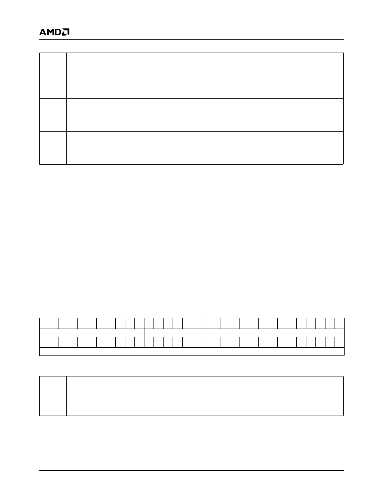
33234H
GLIU Register Descriptions
STATISTIC_ACTION[0:3] Bit Descriptions
Bit Name Description
2 HIT_ASMI Assert ASMI on Descriptor Hit. The descriptor hits are ANDed with the masks and then
all ORed together.
0: Disable.
1: Enable.
1HIT_DEC Decrement Counter on Descriptor Hit. The descriptor hits are ANDed with the masks
and then all ORed together.
0: Disable.
1: Enable.
0HIT_LDEN Load Counter on Descriptor Hit. The descriptor hits are ANDed with the masks and
then all ORed together.
0: Disable.
1: Enable.
4.2.3.4 Request Compare Value (RQ_COMPARE_VAL[0:3]
The RQ Compare Value and the RQ Compare Mask enable traps on specific transactions. A hit to the RQ Compare is
determined by hit = (RQ_IN & RQ_COMPARE_MASK) == RQ_COMPARE_VAL). A hit can trigger the RQ_CMP error
sources when they are enabled. The value is compared only after the packet is arbitrated.
Request Compare Value (RQ_COMPARE_VAL[0])
MSR Address GLIU0: 100000C0h
GLIU1: 400000C0h
Ty p e R / W
Reset Value 001FFFFF_FFFFFFFFh
Request Compare Value (RQ_COMPARE_VAL[1])
MSR Address GLIU0: 100000C2h
GLIU1: 400000C2h
Ty p e R / W
Reset Value 001FFFFF_FFFFFFFFh
Request Compare Value (RQ_COMPARE_VAL[2])
MSR Address GLIU0: 100000C4h
GLIU1: 400000C4h
Ty pe R /W
Reset Value 001FFFFF_FFFFFFFFh
Request Compare Value (RQ_COMPARE_VAL[3])
MSR Address GLIU0: 100000C6h
GLIU1: 400000C6h
Ty pe R /W
Reset Value 001FFFFF_FFFFFFFFh
RQ_COMPARE_VAL[0:3] Register
63 62 61 60 59 58 57 56 55 54 53 52 51 50 49 48 47 46 45 44 43 42 41 40 39 38 37 36 35 34 33 32
RSVD RQ_VAL
313029282726252423222120191817161514131211109876543210
RQ_VAL
RQ_COMPARE_VAL[0:3] Bit Descriptions
Bit Name Description
63:53 RSVD Reserved.
52:0 RQ_VAL Request Packet Value. This is the value compared against the logical bit-wise AND of
the incoming request packet and the RQ_COMPMASK in order to determine a ‘hit”.
74 AMD Geode™ LX Processors Data Book
Page 75

GLIU Register Descriptions
33234H
4.2.3.5 Request Compare Mask (RQ_COMPARE_MASK[0:3]
The RQ Compare Value and the RQ Compare Mask enable traps on specific transactions. A hit to the RQ Compare is
determined by hit = (RQ_IN & RQ_COMPARE_MASK) == RQ_COMPARE_VAL). A hit can trigger the RQ_CMP error
sources when they are enabled. The value is compared only after the packet is arbitrated.
Request Compare Mask (RQ_COMPARE_MASK[0])
MSR Address GLIU0: 100000C1h
GLIU1: 400000C1h
Ty p e R / W
Reset Value 00000000_00000000h
Request Compare Mask (RQ_COMPARE_MASK[1])
MSR Address GLIU0: 100000C3h
GLIU1: 400000C3h
Ty p e R / W
Reset Value 00000000_00000000h
Request Compare Mask (RQ_COMPARE_MASK[2])
MSR Address GLIU0: 100000C5h
GLIU1: 400000C5h
Ty pe R /W
Reset Value 00000000_00000000h
Request Compare Mask (RQ_COMPARE_MASK[3])
MSR Address GLIU0: 100000C7h
GLIU1: 400000C7h
Ty pe R /W
Reset Value 00000000_00000000h
RQ_COMPARE_MASK[0:3] Register Map
63 62 61 60 59 58 57 56 55 54 53 52 51 50 49 48 47 46 45 44 43 42 41 40 39 38 37 36 35 34 33 32
RSVD RQ_MASK
313029282726252423222120191817161514131211109876543210
RQ_MASK
RQ_COMPARE_MASK[0:3] Bit Descriptions
Bit Name Description
63:53 RSVD Reserved.
52:0 RQ_MASK Request Packet Mask. This field is bit-wise logically ANDed with the incoming request
packet before it is compared to the RQ_COMPVAL.
AMD Geode™ LX Processors Data Book 75
Page 76

33234H
GLIU Register Descriptions
4.2.3.6 DA Compare Value Low (DA_COMPARE_VAL_LO[0:3]
The DA Compare Value and the DA Compare Mask enable traps on specific transactions. A hit to the DA Compare is determined by hit = (DA_IN & DA_COMPARE_MASK) == DA_COMPARE_VAL). A hit can trigger the DA_CMP error sources
when they are enabled. The value is compared only after the packet is arbitrated.
Data Compare Value Low (DA_COMPARE_VAL_LO[0])
MSR Address GLIU0: 100000D0h
GLIU1: 400000D0h
Ty p e R / W
Reset Value 00001FFF_FFFFFFFFh
Data Compare Value Low (DA_COMPARE_VAL_LO[1])
MSR Address GLIU0: 100000D4h
GLIU1: 400000D4h
Ty p e R / W
Reset Value 00001FFF_FFFFFFFFh
Data Compare Value Low (DA_COMPARE_VAL_LO[2])
MSR Address GLIU0: 100000D8h
GLIU1: 400000D8h
Ty pe R /W
Reset Value 00001FFF_FFFFFFFFh
Data Compare Value Low (DA_COMPARE_VAL_LO[3])
MSR Address GLIU0: 100000DCh
GLIU1: 400000DCh
Ty pe R /W
Reset Value 00001FFF_FFFFFFFFh
DA_COMPARE_VAL_LO[0:3] Register
63 62 61 60 59 58 57 56 55 54 53 52 51 50 49 48 47 46 45 44 43 42 41 40 39 38 37 36 35 34 33 32
RSVD DALO_VAL
313029282726252423222120191817161514131211109876543210
DALO_VAL
DA_COMPARE_VAL_LO[0:3] Bit Descriptions
Bit Name Description
63:45 RSVD Reserved.
44:0 DALO_VAL DA Packet Compare Value [44:0]. This field forms the lower portion of the data value,
which is compared to the logical bit-wise AND of the incoming data value and the data
value compare mask in order to determine a ‘hit’. The “HI” and “LO” portions of the
incoming data, the compare value, and the compare mask, are assembled into complete
bit patterns before these operations occur.
76 AMD Geode™ LX Processors Data Book
Page 77

GLIU Register Descriptions
33234H
4.2.3.7 DA Compare Value High (DA_COMPARE_VAL_HI[0:3]
The DA Compare Value and the DA Compare Mask enable traps on specific transactions. A hit to the DA Compare is determined by hit = (DA_IN & DA_COMPARE_MASK) == DA_COMPARE_VAL). A hit can trigger the DA_CMP error sources
when they are enabled. The value is compared only after the packet is arbitrated.
Data Compare Value High (DA_COMPARE_VAL_HI[0])
MSR Address GLIU0: 100000D1h
GLIU1: 400000D1h
Ty p e R / W
Reset Value 0000000F_FFFFFFFFh
Data Compare Value High (DA_COMPARE_VAL_HI[1])
MSR Address GLIU0: 100000D5h
GLIU1: 400000D5h
Ty p e R / W
Reset Value 0000000F_FFFFFFFFh
Data Compare Value High (DA_COMPARE_VAL_HI[2])
MSR Address GLIU0: 100000D9h
GLIU1: 400000D9h
Ty pe R /W
Reset Value 0000000F_FFFFFFFFh
Data Compare Value High (DA_COMPARE_VAL_HI[3])
MSR Address GLIU0: 100000DDh
GLIU1: 400000DDh
Ty pe R /W
Reset Value 0000000F_FFFFFFFFh
DA_COMPARE_VAL_HI[0:3] Register Map
63 62 61 60 59 58 57 56 55 54 53 52 51 50 49 48 47 46 45 44 43 42 41 40 39 38 37 36 35 34 33 32
RSVD DAHI_VAL
313029282726252423222120191817161514131211109876543210
DAHI_VAL
DA_COMPARE_VAL_HI[0:3] Bit Descriptions
Bit Name Description
63:36 RSVD Reserved.
35:0 DAHI_VAL DA Packet Compare Value [80:45]. This field forms the upper portion of the data value
which is compared to the logical bit-wise AND of the incoming data value AND the data
value compare mask in order to determine a ‘hit’. The “HI” and “LO” portions of the
incoming data, the compare value, and the compare mask, are assembled into complete
bit patterns before these operations occur.
AMD Geode™ LX Processors Data Book 77
Page 78

33234H
4.2.3.8 DA Compare Mask Low (DA_COMPARE_MASK_LO[0:3])
GLIU Register Descriptions
Data Compare Mask Low
(DA_COMPARE_MASK_LO[0])
MSR Address GLIU0: 100000D2h
GLIU1: 400000D2h
Ty p e R / W
Reset Value 00000000_00000000h
Data Compare Mask Low
(DA_COMPARE_MASK_LO[1])
MSR Address GLIU0: 100000D6h
GLIU1: 400000D6h
Ty p e R / W
Reset Value 00000000_00000000h
Data Compare Mask Low
(DA_COMPARE_MASK_LO[2])
MSR Address GLIU0: 100000DAh
GLIU1: 400000DAh
Ty pe R /W
Reset Value 00000000_00000000h
Data Compare Mask Low
(DA_COMPARE_MASK_LO[3])
MSR Address GLIU0: 100000DEh
GLIU1: 400000DEh
Ty pe R /W
Reset Value 00000000_00000000h
The DA Compare Value and the DA Compare Mask enable traps on specific transactions. A hit to the DA Compare is determined by hit = (DA_IN & DA_COMPARE_MASK) == DA_COMPARE_VAL). A hit can trigger the DA_CMP error sources
when they are enabled. The value is compared only after the packet is arbitrated.
DA_COMPARE_VAL_HI[0:3] Register Map
63 62 61 60 59 58 57 56 55 54 53 52 51 50 49 48 47 46 45 44 43 42 41 40 39 38 37 36 35 34 33 32
RSVD DALO_MASK
31 30 29 28 27 26 25 24 23 22 21 20 19 18 17 16 15 14 13 12 11 10 9 8 7 6 5 4 3 2 1 0
DALO_MASK
DA_COMPARE_MASK_LO[0:3] Bit Descriptions
Bit Name Description
63:45 RSVD Reserved.
44:0 DALO_MASK DA Packet Compare Value [44:0]. This field forms the lower portion of the data COMP-
MASK value, which is then bit-wise logically ANDed with the incoming data value before
it is compared to the DA_COMPVAL. The “HI” and “LO” portions of the incoming data,
the compare value, and the compare mask, are assembled into complete bit patterns
before these operations occur.
78 AMD Geode™ LX Processors Data Book
Page 79

GLIU Register Descriptions
4.2.3.9 DA Compare Mask High (DA_COMPARE_MASK_HI[0:3])
33234H
Data Compare Mask High
(DA_COMPARE_MASK_HI[0])
MSR Address GLIU0: 100000D3h
GLIU1: 400000D3h
Ty p e R / W
Reset Value 00000000_00000000h
Data Compare Mask High
(DA_COMPARE_MASK_HI[1])
MSR Address GLIU0: 100000D7h
GLIU1: 400000D7h
Ty p e R / W
Reset Value 00000000_00000000h
Data Compare Mask High
(DA_COMPARE_MASK_HI[2])
MSR Address GLIU0: 100000DBh
GLIU1: 400000DBh
Ty pe R /W
Reset Value 00000000_00000000h
Data Compare Mask High
(DA_COMPARE_MASK_HI[3])
MSR Address GLIU0: 100000DFh
GLIU1: 400000DFh
Ty pe R /W
Reset Value 00000000_00000000h
DA_COMPARE_MASK_HI[0:3] Register Map
63 62 61 60 59 58 57 56 55 54 53 52 51 50 49 48 47 46 45 44 43 42 41 40 39 38 37 36 35 34 33 32
RSVD DAHI_MASK
31 30 29 28 27 26 25 24 23 22 21 20 19 18 17 16 15 14 13 12 11 10 9 8 7 6 5 4 3 2 1 0
DAHI_MASK
DA_COMPARE_MASK_HI[0:3] Bit Descriptions
Bit Name Description
63:36 RSVD Reserved.
35:0 DAHI_MASK DA Packet Compare Mask [80:45]. This field forms the upper portion of the data
COMPMASK value, which is then bit-wise logically ANDed with the incoming data value
before it is compared to the DA_COMPVAL.The “HI” and “LO” portions of the incoming
data. the compare value, and the compare mask, are assembled into complete bit patterns before these operations occur.
AMD Geode™ LX Processors Data Book 79
Page 80

33234H
GLIU Register Descriptions
4.2.4 P2D Descriptor Registers
P2D descriptors are ordered P2D_BM, P2D_BMO, P2D_R, P2D_RO, P2D_SC, P2D_BMK. For example if NP2D_BM=3
and NP2D_BM0=2, IMSR EO = P2D_BM[0], MSR E3 = P2D_SC[0].
4.2.4.1 P2D Base Mask Descriptor (P2D_BM) GLIU0 P2D_BM[5:0]
MSR Address 10000020h-10000025h
Ty p e R / W
Reset Value 000000FF_FFF00000h
GLIU1 P2D_BM[9:0]
MSR Address 40000020h-40000029h
Ty pe R /W
Reset Value 000000FF_FFF00000h
See Table 4.1.3.1 "Memory Routing and Translation" on page 47 for details on the descriptor usage.
P2D_BM Register Map
63 62 61 60 59 58 57 56 55 54 53 52 51 50 49 48 47 46 45 44 43 42 41 40 39 38 37 36 35 34 33 32
PDID1
PCMP_BIZ
313029282726252423222120191817161514131211109876543210
PBASE PMASK
RSVD PBASE
P2D_BM Bit Descriptions
Bit Name Description
63:61 PDID1 Descriptor Destination ID. These bits define which Port to route the request to, if it is a
‘hit’ based on the other settings in this register.
000: Port 0 (GLIU0 = GLIU; GLIU1 = GLIU.)
001: Port 1 (GLIU0 = GLMC; GLIU1 = Interface to GLIU0.)
010: Port 2 (GLIU0 = Interface to GLIU1; GLIU1 = VP.)
011: Port 3 (GLIU0 = CPU Core; GLIU1 = GLCP.)
100: Port 4 (GLIU0 = DC; GLIU1 = GLPCI.)
101: Port 5 (GLIU0 = GP; GLIU1 = VIP.)
110: Port 6 (GLIU0 = Not Used; GLIU1 = SB.)
111: Port 7 (GLIU0 = Not Used; GLIU1 = Not Used.)
60 PCMP_BIZ Compare Bizzaro Flag.
0: Consider only transactions whose Bizzaro flag is low as a potentially valid address hit.
A low Bizzaro flag indicates a normal transaction cycle such as a memory or I/O.
1: Consider only transactions whose Bizzaro flag is high as a potentially valid address
hit. A high Bizzaro flag indicates a ‘special’ transaction, such as a PCI Shutdown or
Halt cycle.
59:40 RSVD Reserved.
39:20 PBASE Physical Memory Address Base. These bits form the matching value against which the
masked value of the physical address, bits [31:12] are directly compared. If a match is
found, then a “hit’ is declared, depending on the setting of the Bizzaro flag comparator.
19:0 PMASK Physical Memory Address Mask. These bits are used to mask address bits [31:12] for
the purposes of this ‘hit’ detection.
80 AMD Geode™ LX Processors Data Book
Page 81

GLIU Register Descriptions
33234H
4.2.4.2 P2D Base Mask Offset Descriptor (P2D_BMO) GLIU0 P2D_BMO[1:0]
MSR Address 10000026h-10000027h
Ty p e R / W
Reset Value 00000FF0_FFF00000h
See Table 4.1.3.1 "Memory Routing and Translation" on page 47 for details on the descriptor usage.
P2D_BMO Register Map
63 62 61 60 59 58 57 56 55 54 53 52 51 50 49 48 47 46 45 44 43 42 41 40 39 38 37 36 35 34 33 32
PDID1
PCMP_BIZ
31 30 29 28 27 26 25 24 23 22 21 20 19 18 17 16 15 14 13 12 11 10 9 8 7 6 5 4 3 2 1 0
PBASE PMASK
POFFSET PBASE
P2D_BMO Bit Descriptions
Bit Name Description
63:61 PDID1 Descriptor Destination ID. These bits define which Port to route the request to, if it is a
‘hit’ based on the other settings in this register.
000: Port 0 (GLIU0 = GLIU; GLIU1 = GLIU.)
001: Port 1 (GLIU0 = GLMC; GLIU1 = Interface to GLIU0.)
010: Port 2 (GLIU0 = Interface to GLIU1; GLIU1 = VP.)
011: Port 3 (GLIU0 = CPU Core; GLIU1 = GLCP.)
100: Port 4 (GLIU0 = DC; GLIU1 = GLPCI.)
101: Port 5 (GLIU0 = GP; GLIU1 = VIP.)
110: Port 6 (GLIU0 = Not Used; GLIU1 = SB.)
111: Port 7 (GLIU0 = Not Used; GLIU1 = Not Used.)
60 PCMP_BIZ Compare Bizzaro Flag.
0: Consider only transactions whose Bizzaro flag is low as a potentially valid address hit.
A low Bizzaro flag indicates a normal transaction cycle such as a memory or I/O.
1: Consider only transactions whose Bizzaro flag is high as a potentially valid address
hit. A high Bizzaro flag indicates a ‘special’ transaction, such as a PCI Shutdown or
Halt cycle.
59:40 POFFSET Physical Memory Address 2s Comp Offset. 2s complement offset that is added to
physical address on a hit.
39:20 PBASE Physical Memory Address Base. These bits form the matching value against which the
masked value of the physical address, bits [31:12] are directly compared. If a match is
found, then a “hit’ is declared, depending on the setting of the Bizzaro flag comparator.
19:0 PMASK Physical Memory Address Mask. These bits are used to mask address bits [31:12] for
the purposes of this ‘hit’ detection.
AMD Geode™ LX Processors Data Book 81
Page 82

33234H
GLIU Register Descriptions
4.2.4.3 P2D Range Descriptor (P2D_R) GLIU0 P2D_R[0]
MSR Address 10000028h
Ty p e R / W
Reset Value 00000000_000FFFFFh
GLIU1 P2D_R[3:0]
MSR Address 4000002Ah-4000002Dh
Ty pe R /W
Reset Value 00000000_000FFFFFh
See Table 4.1.3.1 "Memory Routing and Translation" on page 47 for details on the descriptor usage.
P2D_R Register Map
63 62 61 60 59 58 57 56 55 54 53 52 51 50 49 48 47 46 45 44 43 42 41 40 39 38 37 36 35 34 33 32
PDID1
PCMP_BIZ
313029282726252423222120191817161514131211109876543210
PMAX PMIN
RSVD PMAX
P2D_R Bit Descriptions
Bit Name Description
63:61 PDID1 Descriptor Destination ID. These bits define which Port to route the request to, if it is a
‘hit’ based on the other settings in this register.
000: Port 0 (GLIU0 = GLIU; GLIU1 = GLIU.)
001: Port 1 (GLIU0 = GLMC; GLIU1 = Interface to GLIU0.)
010: Port 2 (GLIU0 = Interface to GLIU1; GLIU1 = VP.)
011: Port 3 (GLIU0 = CPU Core; GLIU1 = GLCP.)
100: Port 4 (GLIU0 = DC; GLIU1 = GLPCI.)
101: Port 5 (GLIU0 = GP; GLIU1 = VIP.)
110: Port 6 (GLIU0 = Not Used; GLIU1 = SB.)
111: Port 7 (GLIU0 = Not Used; GLIU1 = Not Used.)
60 PCMP_BIZ Compare Bizzaro Flag.
0: Consider only transactions whose Bizzaro flag is low as a potentially valid address hit.
A low Bizzaro flag indicates a normal transaction cycle such as a memory or I/O.
1: Consider only transactions whose Bizzaro flag is high as a potentially valid address
hit. A high Bizzaro flag indicates a ‘special’ transaction, such as a PCI Shutdown or
Halt cycle.
59:40 RSVD Reserved.
39:20 PMAX Physical Memory Address Max. These bits form the value denoting the upper (ending)
address of the physical memory, which is compared to determine a hit.
19:0 PMIN Physical Memory Address Min. These bits form the value denoting the lower (starting)
address of the physical memory, which is compared to determine a hit. Hence, a hit
occurs if the physical address [31:12] >= PMIN and <= PMAX.
82 AMD Geode™ LX Processors Data Book
Page 83

GLIU Register Descriptions
33234H
4.2.4.4 P2D Range Offset Descriptor (P2D_RO) GLIU0 P2D_RO[2:0]
MSR Address 10000029h-1000002Bh
Ty p e R / W
Reset Value 00000000_000FFFFFh
See Table 4.1.3.1 "Memory Routing and Translation" on page 47 for details on the descriptor usage.
P2D_RO Register Map
63 62 61 60 59 58 57 56 55 54 53 52 51 50 49 48 47 46 45 44 43 42 41 40 39 38 37 36 35 34 33 32
PDID1
PCMP_BIZ
31 30 29 28 27 26 25 24 23 22 21 20 19 18 17 16 15 14 13 12 11 10 9 8 7 6 5 4 3 2 1 0
PMAX PMIN
OFFSET PMAX
P2D_RO Bit Descriptions
Bit Name Description
63:61 PDID1 Descriptor Destination ID. These bits define which Port to route the request to, if it is a
‘hit’ based on the other settings in this register.
000: Port 0 (GLIU0 = GLIU; GLIU1 = GLIU.)
001: Port 1 (GLIU0 = GLMC; GLIU1 = Interface to GLIU0.)
010: Port 2 (GLIU0 = Interface to GLIU1; GLIU1 = VP.)
011: Port 3 (GLIU0 = CPU Core; GLIU1 = GLCP.)
100: Port 4 (GLIU0 = DC; GLIU1 = GLPCI.)
101: Port 5 (GLIU0 = GP; GLIU1 = VIP.)
110: Port 6 (GLIU0 = Not Used; GLIU1 = SB.)
111: Port 7 (GLIU0 = Not Used; GLIU1 = Not Used.)
60 PCMP_BIZ Compare Bizzaro Flag.
0: Consider only transactions whose Bizzaro flag is low as a potentially valid address hit.
A low Bizzaro flag indicates a normal transaction cycle such as a memory or I/O.
1: Consider only transactions whose Bizzaro flag is high as a potentially valid address
hit. A high Bizzaro flag indicates a ‘special’ transaction, such as a PCI Shutdown or
Halt cycle.
59:40 POFFSET Physical Memory Address 2’s Comp Offset. 2s complement offset that is added to
physical address on a hit.
39:20 PMAX Physical Memory Address Max. These bits form the value denoting the upper (ending)
address of the physical memory, which is compared to determine a hit.
19:0 PMIN Physical Memory Address Min. These bits form the value denoting the lower (starting)
address of the physical memory, which is compared to determine a hit. Hence, a hit
occurs if the physical address [31:12] >= PMIN and <= PMAX.
AMD Geode™ LX Processors Data Book 83
Page 84

33234H
GLIU Register Descriptions
4.2.4.5 P2D Swiss Cheese Descriptor (P2D_SC) GLIU0 P2D_SC[0]
MSR Address 1000002Ch
Ty p e R / W
Reset Value 00000000_00000000h
GLIU1 P2D_SC[0]
MSR Address 4000002Eh
Ty pe R /W
Reset Value 00000000_00000000h
See Table 4.1.3.1 "Memory Routing and Translation" on page 47 for details on the descriptor usage.
P2D_SC Register Map
63 62 61 60 59 58 57 56 55 54 53 52 51 50 49 48 47 46 45 44 43 42 41 40 39 38 37 36 35 34 33 32
PDID1
PCMP_BIZ
313029282726252423222120191817161514131211109876543210
RSVD WEN
REN
RSVD
PSCBASE
P2D_SC Bit Descriptions
Bit Name Description
63:61 PDID1 Descriptor Destination ID 1. These bits define which Port to route the request to, if it is
a ‘hit’ based on the other settings in this register.
000: Port 0 (GLIU0 = GLIU; GLIU1 = GLIU.)
001: Port 1 (GLIU0 = GLMC; GLIU1 = Interface to GLIU0.)
010: Port 2 (GLIU0 = Interface to GLIU1; GLIU1 = VP.)
011: Port 3 (GLIU0 = CPU Core; GLIU1 = GLCP.)
100: Port 4 (GLIU0 = DC; GLIU1 = GLPCI.)
101: Port 5 (GLIU0 = GP; GLIU1 = VIP.)
110: Port 6 (GLIU0 = Not Used; GLIU1 = SB.)
111: Port 7 (GLIU0 = Not Used; GLIU1 = Not Used.)
60 PCMP_BIZ Compare Bizzaro Flag.
0: Consider only transactions whose Bizzaro flag is low as a potentially valid address hit.
A low Bizzaro flag indicates a normal transaction cycle such as a memory or I/O.
1: Consider only transactions whose Bizzaro flag is high as a potentially valid address
hit. A high Bizzaro flag indicates a ‘special’ transaction, such as a PCI Shutdown or
Halt cycle.
59:48 RSVD Reserved.
47:32 WEN Enable hits to the base for the ith 16K page for writes. When set to 1, causes the
incoming request to be routed to the port specified in PDID1 if the incoming request is a
write type.
31:16 REN Enable hits to the base for the ith 16K page for reads. When set to 1, causes the
incoming request to be routed to the port specified in PDID1 if the incoming request is a
read type.
15:14 RSVD Reserved.
13:0 PBASE Physical Memory Address Base for Hit. These bits form the basis of comparison with
incoming checks that the physical address supplied by the device’s request on address
bits [31:18] are equal to PBASE. Bits [17:14] of the physical address are used to choose
the ith 16K region of WEN/REN for a hit.
84 AMD Geode™ LX Processors Data Book
Page 85

GLIU Register Descriptions
33234H
4.2.5 SPARE MSRs (SPARE_MSR[0:9], A:F)
MSR Address GLIU0: 10000040h-1000004Fh
GLIU1: 40000040h-4000004Fh
Ty p e R / W
Reset Value 00000000_00000000h
SPARE_MSR[x] Register Map
63 62 61 60 59 58 57 56 55 54 53 52 51 50 49 48 47 46 45 44 43 42 41 40 39 38 37 36 35 34 33 32
SPARE_MSR
313029282726252423222120191817161514131211109876543210
SPARE_MSR
SPARE_MSR[x] Bit Descriptions
Bit Name Description
63:0 SPARE_MSR Spare MSR.
AMD Geode™ LX Processors Data Book 85
Page 86

33234H
GLIU Register Descriptions
4.2.6 I/O Descriptors
I/O descriptors are ordered IOD_BM, IOD_SC. For example if NIOD_BM = 3 and NIOD_SC = 2, MSR 100000EOh =
IOD_BM[0] and MSR 100000E3h = IOD_SC[0].
4.2.6.1 IOD Base Mask Descriptors (IOD_BM) GLIU0 IOD_BM[0:3]
MSR Address 100000E0h-100000E2h
Ty p e R / W
Reset Value 000000FF_FFF00000h
GLIU1 IOD_BM[0:3]
MSR Address 400000E0h-400000E2h
Ty pe R /W
Reset Value 000000FF_FFF00000h
See Table 4.1.3.1 "Memory Routing and Translation" on page 47 for details on the descriptor usage.
IOD_BM[x] Register Map
63 62 61 60 59 58 57 56 55 54 53 52 51 50 49 48 47 46 45 44 43 42 41 40 39 38 37 36 35 34 33 32
IDID
ICMP_BIZ
313029282726252423222120191817161514131211109876543210
IBASE IMASK
RSVD IBASE
IOD_BM[x] Bit Descriptions
Bit Name Description
63:61 IDID I/O Descriptor Destination ID. These bits define which Port to route the request to, if it
is a ‘hit’ based on the other settings in this register.
000: Port 0 (GLIU0 = GLIU; GLIU1 = GLIU.)
001: Port 1 (GLIU0 = GLMC; GLIU1 = Interface to GLIU0.)
010: Port 2 (GLIU0 = Interface to GLIU1; GLIU1 = VP.)
011: Port 3 (GLIU0 = CPU Core; GLIU1 = GLCP.)
100: Port 4 (GLIU0 = DC; GLIU1 = GLPCI.)
101: Port 5 (GLIU0 = GP; GLIU1 = VIP.)
110: Port 6 (GLIU0 = Not Used; GLIU1 = SB.)
111: Port 7 (GLIU0 = Not Used; GLIU1 = Not Used.)
60 ICMP_BIZ Compare Bizzaro Flag.
0: Consider only transactions whose Bizzaro flag is low as a potentially valid address hit.
A low Bizzaro flag indicates a normal transaction cycle such as a memory or I/O.
1: Consider only transactions whose Bizzaro flag is high as a potentially valid address
hit. A high Bizzaro flag indicates a ‘special’ transaction, such as a PCI Shutdown or
Halt cycle.
59:40 RSVD Reserved.
39:20 IBASE Physical I/O Address Base. These bits form the matching value against which the
masked value of the physical address, bits [19:0] are directly compared. If a match is
found, then a “hit’ is declared, depending on the setting of the Bizzaro flag comparator.
19:0 IMASK Physical I/O Address Mask. These bits are used to mask address bits [31:12] for the
purposes of this ‘hit’ detection.
86 AMD Geode™ LX Processors Data Book
Page 87
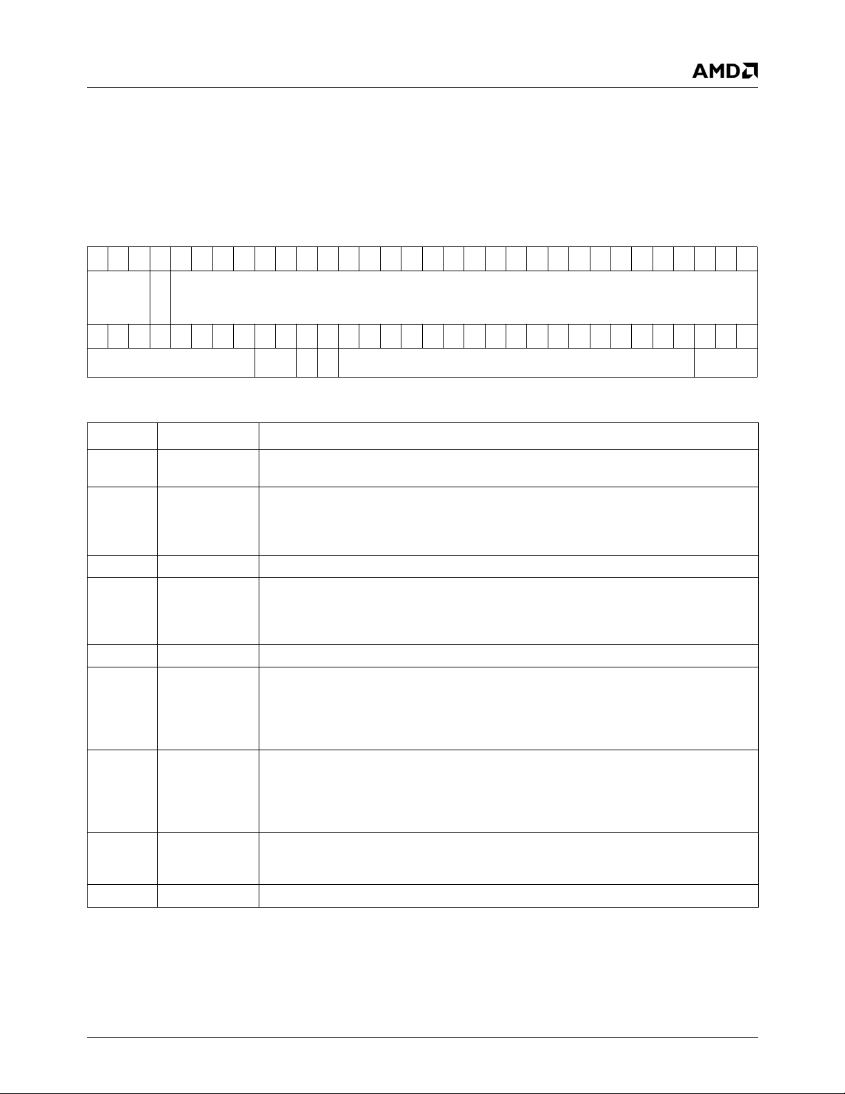
GLIU Register Descriptions
33234H
4.2.6.2 IOD Swiss Cheese Descriptors (IOD_SC) GLIU0 IOD_SC[0:5]
MSR Address 100000E3h-100000E8h
Ty p e R / W
Reset Value 00000000_00000000h
GLIU1 IOD_SC[0:3]
MSR Address 400000E3h-400000E6h
Ty pe R /W
Reset Value 00000000_00000000h
See Table 4.1.3.1 "Memory Routing and Translation" on page 47 for details on the descriptor usage.
IOD_SC[x] Register Map
63 62 61 60 59 58 57 56 55 54 53 52 51 50 49 48 47 46 45 44 43 42 41 40 39 38 37 36 35 34 33 32
IDID1
ICMP_BIZ
313029282726252423222120191817161514131211109876543210
EN RSVD
REN
WEN
RSVD
IBASE RSVD
IOD_SC[x] Bit Descriptions
Bit Name Description
63:61 IDID1 Descriptor Destination ID 1. Encoded port number of the destination of addresses
which produce a ‘hit’ based on the other fields in this descriptor.
60 ICMP_BIZ Compare Bizzaro Flag. Used to check that the Bizzaro flag of the request is equal to
the PICMP_BIZ_SC bit (this bit). If a match does not occur, then the incoming request
cannot generate a hit. The Bizzaro flag, if set in the incoming request, signifies a “special’ cycle such as a PCI Shutdown or Halt.
59:32 RSVD Reserved. Write as read.
31:24 EN Enable for Hits to IDID1 or else SUBP. Setting these bits enables hits to IDID1. If not
enabled, subtractive port is selected per GLD_MSR_CONFIG, bits [2:0] (MSR GLIU0:
10002001h; GLIU1: 40002001h). (See Section 4.2.1.2 "GLD Master Configuration MSR
(GLD_MSR_CONFIG)" on page 55 for bit descriptions).
23:22 RSVD Reserved.
21 WEN Descriptor Hits IDID1 on Write Request Types else SUBP. If set, causes the incom-
ing request to be routed to the port specified in IDID1 if the incoming request is a Write
type. If not set, subtractive port is selected per GLD_MSR_CONFIG, bits [2:0] (MSR
GLIU0: 10002001h; GLIU1: 40002001h). (See Section 4.2.1.2 "GLD Master Configuration MSR (GLD_MSR_CONFIG)" on page 55 for bit descriptions).
20 REN Descriptors Hit IDID1 on Read Request Types else SUBP. If set, causes the incom-
ing request to be routed to the port specified in IDID1 if the incoming request is a Read
type. If not set, subtractive port is selected per GLD_MSR_CONFIG, bits [2:0] (MSR
GLIU0: 10002001h; GLIU1: 40002001h). (See Section 4.2.1.2 "GLD Master Configuration MSR (GLD_MSR_CONFIG)" on page 55 for bit descriptions).
19:3 IBASE I/O Memory Base. This field forms the basis of comparison with the incoming checks
that the physical address supplied by the device’s request on address bits [31:18] are
equal to the PBASE field of descriptor register bits [13:0].
2:0 RSVD Reserved. Write as read.
AMD Geode™ LX Processors Data Book 87
Page 88

33234H
GLIU Register Descriptions
88 AMD Geode™ LX Processors Data Book
Page 89

CPU Core 33234H
5.0CPU Core
5
This section describes the internal operations of the
AMD Geode™ LX processor’s CPU Core from a programmer’s point of view. It includes a description of the traditional “core” processing and FPU operations. The
integrated function registers are described in the next
chapter.
The primary register sets within the processor core include:
• Application Register Set
• System Register Set
5.1 Core Processor Initialization
The CPU Core is initialized when the RESET# (Reset) signal is asserted. The CPU Core is placed in real mode and
the registers listed in Table 5-1 are set to their initialized
values. RESET# invalidates and disables the CPU cache,
Table 5-1. Initialized Core Register Controls
Initialized Contents
Register Register Name
EAX Accumulator xxxxxxxxh 00000000h indicates self-test passed.
EBX Base xxxxxxxxh
ECX Count xxxxxxxxh
EDX Data xxxx 04 [DIR0]h DIR0 = Device ID
EBP Base Pointer xxxxxxxxh
ESI Source Index xxxxxxxxh
EDI Destination Index xxxxxxxxh
ESP Stack Pointer xxxxxxxxh
EFLAGS Extended Flags 00000002h See Table 5-4 on page 93 for bit definitions.
EIP Instruction Pointer 0000FFF0h
ES Extra Segment 0000h Base address set to 00000000h. Limit set to FFFFh.
CS Code Segment F000h Base address set to FFFF0000h. Limit set to FFFFh.
SS Stack Segment 0000h Base address set to 00000000h. Limit set to FFFFh.
DS Data Segment 0000h Base address set to 00000000h. Limit set to FFFFh.
FS Extra Segment 0000h Base address set to 00000000h. Limit set to FFFFh.
GS Extra Segment 0000h Base address set to 00000000h. Limit set to FFFFh.
IDTR Interrupt Descriptor Table Register Base = 0, Limit = 3FFh
GDTR Global Descriptor Table Register xxxxxxxxh
LDTR Local Descriptor Table Register xxxxh
TR Task Register xxxxh
CR0 Control Register 0 60000010h See Table 5-10 on page 96 for bit descriptions.
CR2 Control Register 2 xxxxxxxxh See Table 5-9 on page 96 for bit descriptions.
CR3 Control Register 3 xxxxxxxxh See Table 5-8 on page 96 for bit descriptions.
CR4 Control Register 4 00000000h See Table 5-7 on page 96 for bit descriptions.
Note 1. x = Undefined value.
(Note 1) Comments
and turns off paging. When RESET# is asserted, the CPU
terminates all local bus activity and all internal execution.
While RESET# is asserted, the internal pipeline is flushed
and no instruction execution or bus activity occurs.
Approximately 150 to 250 external clock cycles after
RESET# is de-asserted, the processor begins executing
instructions at the top of physical memory (address location
FFFFFFF0h). The actual number of clock cycles depends
on the clock scaling in use. Also, before execution begins,
an additional 2
requested.
Typically, an intersegment jump is placed at FFFFFFF0h.
This instruction forces the processor to begin execution in
the lowest 1 MB of address space. Table 5-1 lists the CPU
Core registers and illustrates how they are initialized.
20
clock cycles are needed when self-test is
AMD Geode™ LX Processors Data Book 89
Page 90

33234H
CPU Core
5.2 Instruction Set Overview
The CPU Core instruction set can be divided into nine
types of operations:
• Arithmetic
• Bit Manipulation
• Shift/Rotate
• String Manipulation
• Control Transfer
• Data Transfer
• Floating Point
• High-Level Language Support
• Operating System Support
The instructions operate on as few as zero operands and
as many as three operands. A NOP (no operation) instruction is an example of a zero-operand instruction. Two-operand instructions allow the specification of an explicit source
and destination pair as part of the instruction. These twooperand instructions can be divided into ten groups according to operand types:
• Register to Register
• Register to Memory
• Memory to Register
• Memory to Memory
• Register to I/O
• I/O to Register
• Memory to I/O
• I/O to Memory
• Immediate Data to Register
• Immediate Data to Memory
An operand can be held in the instruction itself (as in the
case of an immediate operand), in one of the processor’s
registers or I/O ports, or in memory. An immediate operand
is fetched as part of the opcode for the instruction.
Operand lengths of 8, 16, 32 or 48 bits are supported as
well as 64 or 80 bits associated with floating-point instructions. Operand lengths of 8 or 32 bits are generally used
when executing code written for 386- or 486-class (32-bit
code) processors. Operand lengths of 8 or 16 bits are generally used when executing existing 8086 or 80286 code
(16-bit code). The default length of an operand can be
overridden by placing one or more instruction prefixes in
front of the opcode. For example, the use of prefixes allows
a 32-bit operand to be used with 16-bit code or a 16-bit
operand to be used with 32-bit code.
The Processor Core Instruction Set (see Table 8-26 on
page 634) contains the clock count table that lists each
instruction in the CPU instruction set. Included in the table
are the associated opcodes, execution clock counts, and
effects on the EFLAGS register.
5.2.1 Lock Prefix
The LOCK prefix may be placed before certain instructions
that read, modify, then write back to memory. The PCI will
not be granted access in the middle of locked instructions.
The LOCK prefix can be used with the following instructions
only when the result is a write operation to memory.
• Bit Test Instructions (BTS, BTR, BTC)
• Exchange Instructions (XADD, XCHG, CMPXCHG)
• One-Operand Arithmetic and Logical Instructions (DEC,
INC, NEG, NOT)
• Two-Operand Arithmetic and Logical Instructions (ADC,
ADD, AND, OR, SBB, SUB, XOR).
An invalid opcode exception is generated if the LOCK prefix is used with any other instruction or with one of the
instructions above when no write operation to memory
occurs (for example, when the destination is a register).
5.2.2 Register Sets
The accessible registers in the processor are grouped into
two sets:
1) The Application Register Set contains the registers
frequently used by application programmers. Table 5-2
on page 91 shows the General Purpose, Segment,
Instruction Pointer and EFLAGS registers.
2) The System Register Set contains the registers typi-
cally reserved for operating systems programmers:
Control, System Address, Debug, Configuration, and
Test registers. All accesses to the these registers use
special CPU instructions.
Both of these register sets are discussed in detail in the
subsections that follow.
90 AMD Geode™ LX Processors Data Book
Page 91

CPU Core
33234H
5.3 Application Register Set
The Application Register Set consists of the registers most
often used by the applications programmer. These registers are generally accessible, although some bits in the
EFLAGS registers are protected.
The General Purpose register contents are frequently
modified by instructions and typically contain arithmetic
and logical instruction operands.
In real mode, Segment registers contain the base
address for each segment. In protected mode, the Segment registers contain segment selectors. The segment
selectors provide indexing for tables (located in memory)
Table 5-2. Application Register Set
313029282726252423222120191817161514131211109876543210
General Purpose Registers
EAX (Extended A Register)
EBX (Extended B Register)
ECX (Extended C Register)
EDX (Extended D Register)
ESI (Extended Source Index)
EDI (Extended Destination Index)
EBP (Extended Base Pointer)
ESP (Extended Stack Pointer)
Segment (Selector) Registers
Instruction Pointer and EFLAGS Registers
EIP (Extended Instruction Pointer)
ESP (Extended EFLAGS Register)
that contain the base address for each segment, as well as
other memory addressing information.
The Instruction Pointer register points to the next instruction that the processor will execute. This register is automatically incremented by the processor as execution
progresses.
The EFLAGS register contains control bits used to reflect
the status of previously executed instructions. This register
also contains control bits that affect the operation of some
instructions.
AX
AH AL
BX
BH BL
CX
CH CL
DX
DH DL
SI (Source Index)
DI (Destination Index)
BP (Base Pointer)
SP (Stack Pointer)
CS (Code Segment)
SS (Stack Segment)
DS (D Data Segment)
ES (E Data Segment)
FS (F Data Segment)
GS (G Data Segment)
AMD Geode™ LX Processors Data Book 91
Page 92

33234H
CPU Core
5.3.1 General Purpose Registers
The General Purpose registers are divided into four data
registers, two pointer registers, and two index registers as
shown in Table 5-2 on page 91.
The Data registers are used by the applications programmer to manipulate data structures and to hold the results of
logical and arithmetic operations. Different portions of general data registers can be addressed by using different
names.
An “E” prefix identifies the complete 32-bit register. An “X”
suffix without the “E” prefix identifies the lower 16 bits of the
register.
The lower two bytes of a data register are addressed with
an “H” suffix (identifies the upper byte) or an “L” suffix (identifies the lower byte). These _L and _H portions of the data
registers act as independent registers. For example, if the
AH register is written to by an instruction, the AL register
bits remain unchanged.
The Pointer and Index registers are listed below.
SI or ESI Source Index
DI or EDI Destination Index
SP or ESP Stack Pointer
BP or EBP Base Pointer
These registers can be addressed as 16- or 32-bit registers,
with the “E” prefix indicating 32 bits. The Pointer and Index
registers can be used as general purpose registers; however, some instructions use a fixed assignment of these
registers. For example, repeated string operations always
use ESI as the source pointer, EDI as the destination
pointer, and ECX as a counter. The instructions that use
fixed registers include multiply and divide, I/O access,
string operations, stack operations, loop, variable shift and
rotate, and translate instructions.
The CPU Core implements a stack using the ESP register.
This stack is accessed during the PUSH and POP instructions, procedure calls, procedure returns, interrupts, exceptions, and interrupt/exception returns. The Geode LX
processor automatically adjusts the value of the ESP during operations that result from these instructions.
The EBP register may be used to refer to data passed on
the stack during procedure calls. Local data may also be
placed on the stack and accessed with BP. This register
provides a mechanism to access stack data in high-level
languages.
5.3.2 Segment Registers
The 16-bit Segment registers are part of the main memory
addressing mechanism. The six segment registers are:
CS - Code Segment
DS - Data Segment
SS - Stack Segment
ES - Extra Segment
FS - Additional Data Segment
GS - Additional Data Segment
The Segment registers are used to select segments in
main memory. A segment acts as private memory for different elements of a program such as code space, data space
and stack space. There are two segment mechanisms, one
for real and virtual 8086 operating modes and one for protected mode.
The active Segment register is selected according to the
rules listed in Table 5-3 and the type of instruction being
currently processed. In general, the DS register selector is
used for data references. Stack references use the SS register, and instruction fetches use the CS register. While
some selections may be overridden, instruction fetches,
stack operations, and the destination write operation of
string operations cannot be overridden. Special segmentoverride instruction prefixes allow the use of alternate segment registers. These segment registers include the ES,
FS, and GS registers.
5.3.3 Instruction Pointer Register
The Instruction Pointer (EIP) register contains the offset
into the current code segment of the next instruction to be
executed. The register is normally incremented by the
length of the current instruction with each instruction execution unless it is implicitly modified through an interrupt,
exception, or an instruction that changes the sequential
execution flow (for example JMP and CALL).
Table 5-3. Segment Register Selection Rules
Implied (Default)
Type of Memory Reference
Code Fetch CS None
Destination of PUSH, PUSHF, INT, CALL, PUSHA instructions SS None
Source of POP, POPA, POPF, IRET, RET instructions SS None
Destination of STOS, MOVS, REP STOS, REP MOVS instructions ES None
Other data references with effective address using base registers of:
EAX, EBX, ECX, EDX, ESI, EDI, EBP, ESP
92 AMD Geode™ LX Processors Data Book
Segment
DS
SS
Segment-Override
Prefix
CS, ES, FS, GS, SS
CS, DS, ES, FS, GS
Page 93

CPU Core
33234H
5.3.4 EFLAGS Register
The EFLAGS register contains status information and controls certain operations on the Geode LX processor. The
lower 16 bits of this register are used when executing 8086
or 80286 code. Table 5-4 gives the bit formats for the
EFLAGS register.
Table 5-4. EFLAGS Register
Bit Name Flag Type Description
31:22 RSVD -- Reserved. Set to 0.
21 ID System Identification Bit. The ability to set and clear this bit indicates that the CPUID instruction is sup-
ported. The ID can be modified only if the CPUID bit in CCR4 (Index E8h[7]) is set.
20:19 RSVD -- Reserved. Set to 0.
18 AC System Alignment Check Enable. In conjunction with the AM flag (bit 18) in CR0, the AC flag deter-
mines whether or not misaligned accesses to memory cause a fault. If AC is set, alignment
faults are enabled.
17 VM System Virtual 8086 Mode. If set while in protected mode, the processor switches to virtual 8086 oper-
ation handling segment loads as the 8086 does, but generating exception 13 faults on privileged
opcodes. The VM bit can be set by the IRET instruction (if current privilege level is 0) or by task
switches at any privilege level.
16 RF Debug Resume Flag. Used in conjunction with debug register breakpoints. RF is checked at instruction
boundaries before breakpoint exception processing. If set, any debug fault is ignored on the next
instruction.
15 RSVD -- Reserved. Set to 0.
14 NT System Nested Task. While executing in protected mode, NT indicates that the execution of the current
task is nested within another task.
13:12 IOPL System I/O Privilege Level. While executing in protected mode, IOPL indicates the maximum current
privilege level (CPL) permitted to execute I/O instructions without generating an exception 13
fault or consulting the I/O permission bit map. IOPL also indicates the maximum CPL allowing
alteration of the IF bit when new values are popped into the EFLAGS register.
11 OF Arithmetic Overflow Flag. Set if the operation resulted in a carry or borrow into the sign bit of the result but
did not result in a carry or borrow out of the high-order bit. Also set if the operation resulted in a
carry or borrow out of the high-order bit but did not result in a carry or borrow into the sign bit of
the result.
10 DF Control Direction Flag. When cleared, DF causes string instructions to auto-increment (default) the
9 IF System Interrupt Enable Flag. When set, maskable interrupts (INTR input pin) are acknowledged and
8 TF Debug Trap Enable Flag. Once set, a single-step interrupt occurs after the next instruction completes
7 SF Arithmetic Sign Flag. Set equal to high-order bit of result (0 indicates positive, 1 indicates negative).
6 ZF Arithmetic Zero Flag. Set if result is zero; cleared otherwise.
5 RSVD -- Reserved. Set to 0.
4 AF Arithmetic Auxiliary Carry Flag. Set when a carry out of (addition) or borrow into (subtraction) bit position
3 RSVD -- Reserved. Set to 0.
2 PF Arithmetic Parity Flag. Set when the low-order 8 bits of the result contain an even number of ones; other-
1 RSVD Reserved. Set to 1.
0 CF Arithmetic Carry Flag. Set when a carry out of (addition) or borrow into (subtraction) the most significant
appropriate index registers (ESI and/or EDI). Setting DF causes auto-decrement of the index
registers to occur.
serviced by the CPU.
execution. TF is cleared by the single-step interrupt.
3 of the result occurs; cleared otherwise.
wise PF is cleared.
bit of the result occurs; cleared otherwise.
AMD Geode™ LX Processors Data Book 93
Page 94

33234H
5.4 System Register Set
The System Register Set, shown in Table 5-5, consists of
registers not generally used by application programmers.
These registers are either initialized by the system BIOS or
employed by system level programmers who generate
operating systems and memory management programs.
Associated with the System Register Set are certain tables
and registers that are listed in Table 5-5.
The Control registers control certain aspects of the CPU
Core such as paging, coprocessor functions, and segment
protection.
The CPU Core Configuration registers are used to initialize, provide for, test or define most of the features of the
CPU Core. The attributes of these registers include:
• CPU setup - Enable cache, features, operating modes.
• Debug support - Provide debugging facilities for the
Geode™ LX processor and enable the use of data
access breakpoints and code execution breakpoints.
• Built-in Self-test (BIST) support.
• Test - Support a mechanism to test the contents of the
on-chip caches and the Translation Lookaside Buffers
(TLBs).
• In-Circuit Emulation (ICE) - Provide for a alternative
accessing path to support an ICE.
• CPU identification - Allow the BIOS and other software
to identify the specific CPU and stepping.
• Power Management.
• Performance Monitoring - Enables test software to
measure the performance of application software.
The Descriptor Table registers point to tables used to
manage memory segments and interrupts.
Table 5-5. System Register Set
Group Name Function
Control
Registers
CPU Core
Configuration
Registers
Descriptor
Ta bl e
Registers
Task Register
Performance
Registers
CR0 System Control
Register
CR2 Page Fault Linear
Address Register
CR3 Page Directory Base
Register
CR4 Feature Enables 32
PLn Pipeline
Control Registers
IMn Instruction Memory
Control Registers
DMn Data Memory Con-
trol Registers
BCn Bus Controller Con-
trol Registers
FPUn Floating Point Unit
Shadow Registers
GDTR GDT Register 32
IDTR IDT Register 32
LDTR LDT Register 16
TR Task Register 16
PCRn Performance
Control Registers
CPU Core
Width
(Bits)
32
32
32
64
64
64
64
64
8
The Task State register points to the Task State Segment,
which is used to save and load the processor state when
switching tasks.
Table 5-5 lists the System Register Sets along with their
size and function.
94 AMD Geode™ LX Processors Data Book
Page 95

CPU Core
33234H
5.4.1 Control Registers
A map of the Control registers (CR0, CR1, CR2, CR3, and
CR4) is shown in Table 5-6 and the bit descriptions are in
the tables that follow. (These registers should not be confused with the CRRn registers.) CR0 contains system control bits that configure operating modes and indicate the
general state of the CPU. The lower 16 bits of CR0 are
referred to as the Machine Status Word (MSW).
When operating in real mode, any program can read and
write the control registers. In protected mode, however,
only privilege level 0 (most-privileged) programs can read
and write these registers.
L1 Cache Controller
The CD bit (Cache Disable, bit 30) in CR0 globally controls
the operating mode of the L1 and L2 caches. LCD and
LWT, Local Cache Disable and Local Write-through bits in
the Translation Lookaside Buffer, control the mode on a
page-by-page basis. Additionally, memory configuration
control can specify certain memory regions as non-cacheable.
If the cache is disabled, no further cache line fills occur.
However, data already present in the cache continues to be
used. For the cache to be completely disabled, the cache
must be invalidated with a WBINVD instruction after the
cache has been disabled.
Write-back caching improves performance by relieving congestion on slower external buses.
The Geode LX processor contains an on-board 64 KB L1
instruction cache, a 64 KB L1 write-back data cache, and a
128 KB unified L2 victim cache. With the memory controller
on-board, the L1 cache requires no external logic to main-
The Geode LX processor caches SMM regions, reducing
system management overhead to allow for hardware emulation such as VGA.
tain coherency. All DMA cycles automatically snoop the L1
and L2 caches.
Table 5-6. Control Registers Map
313029282726252423222120191817161514131211109876543210
CR4 Register Control Register 4 (R/W)
RSVD
CR3 Register Control Register 3 (R/W)
PDBR (Page Directory Base Register) RSVD 0 0 RSVD
CR2 Register Control Register 2 (R/W)
PFLA (Page Fault Linear Address)
CR1 Register Control Register 1 (R/W)
CR0 Register Control Register 0 (R/W)
RSVD
PG
CD
NW
AM
RSVD
WP
RSVD
RSVD
Machine Status Word (MSW)
PCE
RSVD
PGE
PSEDETSC
NE
RSVD
TS
RSVD
EM
MP
PE
AMD Geode™ LX Processors Data Book 95
Page 96

33234H
CPU Core
Table 5-7. CR4 Bit Descriptions
Bit Name Description
31:9 RSVD Reserved. Set to 0 (always returns 0 when read).
8PCE Performance Counter Enable. Set PCE = 1 to make RDPMC available at nonzero privi-
lege levels.
7PGE Page Global Enable. Set PGE = 1 to make global pages immune to INVLPG instruc-
tions.
6:5 RSVD Reserved. Set to 0 (always returns 0 when read).
4 PSE Page Size Extensions. Set PSE = 1 to enable 4 MB pages.
3DE Debug Extensions. Set DE = 1 to enable debug extensions (i.e., DR4, DR5, and I/O
breakpoints).
2TSC Time Stamp Counter Instruction.
0: RDTSC instruction enabled for all CPL states.
1: RDTSC instruction enabled for CPL = 0 only.
1:0 RSVD Reserved. Set to 0 (always returns 0 when read).
Table 5-8. CR3 Bit Descriptions
Bit Name Description
31:12 PDBR Page Directory Base Register. Identifies page directory base address on a 4 KB page
boundary.
11:0 RSVD Reserved. Set to 0.
Table 5-9. CR2 Bit Descriptions
Bit Name Description
31:0 PFLA Page Fault Linear Address. With paging enabled and after a page fault, PFLA contains
the linear address of the address that caused the page fault.
Table 5-10. CR0 Bit Descriptions
Bit Name Description
31 PG Paging Enable Bit. If PG = 1 and protected mode is enabled (PE = 1), paging is
enabled. After changing the state of PG, software must execute an unconditional branch
instruction (e.g., JMP, CALL) to have the change take effect.
96 AMD Geode™ LX Processors Data Book
Page 97

CPU Core
33234H
Table 5-10. CR0 Bit Descriptions (Continued)
Bit Name Description
30 CD Cache Disable/Not Write-Through (Snoop). Cache behavior is based on the CR0 CD
29 NW
28:19 RSVD Reserved.
18 AM Alignment Check Mask. If AM = 1, the AC bit in the EFLAGS register is unmasked and
17 RSVD Reserved
16 WP Write Protect. Protects read only pages from supervisor write access. WP = 0 allows a
15:6 RSVD Reserved.
5NE Numerics Exception. NE = 1 to allow FPU exceptions to be handled by interrupt 16.
4ET (RO) Extension Type (Read Only). (Default = 1)
3TS Task Switched. Set whenever a task switch operation is performed. Execution of a float-
2EM Emulate Processor Extension. If EM = 1, all floating point instructions cause a DNA
1MP Monitor Processor Extension. If MP = 1 and TS = 1, a WAIT instruction causes DNA
0PE Protected Mode Enable. Enables the segment based protection mechanism. If PE = 1,
Note 1. For effects of various combinations of the TS, EM, and MP bits, see Table 5-11 on page 98.
and NW bits.
CD NW
0 0 Normal Cache operation, coherency maintained.
Read hits access the cache,
Write hits update the cache,
Read/write misses may cause line allocations based on memory
region configuration settings.
0 1 Invalid, causes a General Protection Fault (GPF).
1 0 Cache off, coherency maintained (i.e., snooping enabled).
Read hits access the cache,
Write hits update the cache,
Read/write misses do not cause line allocations.
1 1 Cache off, coherency not maintained (i.e., snooping disabled).
Read hits access the cache,
Write hits update the cache,
Read/write misses do not cause line allocations.
allowed to enable alignment check faults. Setting AM = 0 prevents AC faults from occurring.
read only page to be written from privilege level 0-2. WP = 1 forces a fault on a write to a
read only page from any privilege level.
NE = 0 if FPU exceptions are to be handled by external interrupts.
ing point instruction with TS = 1 causes a Device Not Available (DNA) fault. If MP = 1 and
TS = 1, a WAIT instruction also causes a DNA fault. (Note 1)
fault 7. (Note 1)
fault 7. The TS bit is set to 1 on task switches by the CPU. Floating point instructions are
not affected by the state of the MP bit. The MP bit should be set to 1 during normal operations. (Note 1)
protected mode is enabled. If PE = 0, the CPU operates in real mode and addresses are
formed as in an 8086-style CPU.
AMD Geode™ LX Processors Data Book 97
Page 98
33234H
CPU Core
Table 5-11. Effects of Various Combinations of EM, TS, and MP Bits
CR0[3:1] Instruction Type
TS EM MP WAIT ESC
000 Execute Execute
001 Execute Execute
1 0 0 Execute Fault 7
101 Fault 7 Fault 7
0 1 0 Execute Fault 7
0 1 1 Execute Fault 7
1 1 0 Execute Fault 7
111 Fault 7 Fault 7
98 AMD Geode™ LX Processors Data Book
Page 99

CPU Core Register Descriptions
33234H
5.5 CPU Core Register Descriptions
All CPU Core registers are Model Specific Registers
(MSRs) and are accessed via the RDMSR and WRMSR
instructions.
Each module inside the processor is assigned a 256 register section of the address space. The module responds to
any reads or writes in that range. Unused addresses within
a module’s address space are reserved, meaning the module returns zeroes on a read and ignores writes. Addresses
that are outside all the module address spaces are invalid,
Table 5-12. Standard GeodeLink™ Device MSRs Summary
MSR
Address Type Register Name Reset Value Reference
00002000h RO GLD Capabilities MSR (GLD_MSR_CAP) 00000000_000864xxh Page 108
00002001h R/W GLD Master Configuration MSR
(GLD_MSR_CONFIG)
00002002h R/W GLD SMI MSR (GLD_MSR_SMI) - Not Used 00000000_00000000h Page 109
00002003h R/W GLD Error MSR (GLD_MSR_ERROR) - Not Used 00000000_00000000h Page 109
00002004h R/W GLD Power Management MSR (GLD_MSR_PM) -
Not Used
00002005h R/W GLD Diagnostic Bus Control MSR
(GLD_MSR_DIAG)
meaning a RDMSR/WRMSR instruction attempting to use
the address generates a General Protection Fault.
The registers associated with the CPU Core are the Standard GeodeLink™ Device MSRs and CPU Core Specific
MSRs. Table 5-12 and Table 5-13 are register summary
tables that include reset values and page references where
the bit descriptions are provided. Note that the standard
GLD MSRs for the CPU Core start at 00002000h.
00000000_00000320h Page 108
00000000_00000000h Page 109
00000000_00000000h Page 109
Table 5-13. CPU Core Specific MSRs Summary
MSR
Address Type Register Name Reset Value Reference
00000010h R/W Time Stamp Counter MSR (TSC_MSR) 00000000_00000000h Page 110
000000C1h R/W Performance Event Counter 0 MSR
(PERF_CNT0_MSR)
000000C2h R/W Performance Event Counter 1 MSR
(PERF_CNT1_MSR)
00000174h R/W SYSENTER/SYSEXIT Code Segment Selector
MSR (SYS_CS_MSR)
00000175h R/W SYSENTER/SYSEXIT Stack Pointer MSR
(SYS_SP_MSR)
00000176h R/W SYSENTER/SYSEXIT Instruction Pointer MSR
(SYS_IP_MSR)
00000186h R/W Performance Event Counter 0 Select MSR
(PERF_SEL0_MSR
00000187h R/W Performance Event Counter 1 Select MSR
(PERF_SEL1_MSR)
00001100h R/W Instruction Fetch Configuration MSR
(IF_CONFIG_MSR)
00001102h W IF Invalidate MSR (IF_INVALIDATE_MSR) 00000000_00000000h Page 118
00001108h R/W IF Test Address MSR (IF_TEST_ADDR_MSR) 00000000_00000000h Page 118
00001109h R/W IF Test Data MSR (IF_TEST_DATA_MSR) 00000000_xxxxxxxxh Page 119
00000000_00000000h Page 110
00000000_00000000h Page 111
00000000_C09B0000h Page 112
00000000_00000000h Page 113
00000000_00000000h Page 113
00000000_00000000h Page 114
00000000_00000000h Page 114
00000000_00005051h Page 115
AMD Geode™ LX Processors Data Book 99
Page 100

33234H
CPU Core Register Descriptions
Table 5-13. CPU Core Specific MSRs Summary (Continued)
MSR
Address Type Register Name Reset Value Reference
00001110h RO IF Sequential Count MRS (IF_SEQCOUNT_MSR) 00000000_00000000h Page 122
00001140h RO IF Built-In Self-Test MSR (IF_BIST_MSR) 00000000_00000000h Page 123
00001210h R/W Exception Unit (XC) Configuration MSR
(XC_CONFIG_MSR)
00001211h R/W XC Mode MSR (XC_MODE_MSR) 00000000_00000000h Page 125
00001212h RO XC History MSR (XC_HIST_MSR) 00000000_00000000h Page 126
00001213h RO XC Microcode Address MSR (XC_UADDR_MSR) 00000000_00000000h Page 127
00001250h R/W ID Configuration MSR (ID_CONFIG_MSR) 00000000_00000002h Page 127
00001301h R/W SMM Control MSR (SMM_CTL_MSR) 00000000_00000000h Page 128
00001302h R/W Debug Management Interrupt (DMI) Control Reg-
ister
00001310h R/W Temporary 0 MSR (TEMP0_MSR) xxxxxxxx_xxxxxxxxh Page 130
00001311h R/W Temporary 1 MSR (TEMP1_MSR) xxxxxxxx_xxxxxxxxh Page 130
00001312h R/W Temporary 2 MSR (TEMP2_MSR) xxxxxxxx_xxxxxxxxh Page 130
00001313h R/W Temporary 3 MSR (TEMP3_MSR) xxxxxxxx_xxxxxxxxh Page 130
00001320h R/W ES Segment Selector/Flags Register
(ES_SEL_MSR)
00001321h R/W CS Segment Selector/Flags Register
(CS_SEL_MSR)
00001322h R/W SS Segment Selector/Flags Register
(SS_SEL_MSR)
00001323h R/W DS Segment Selector/Flags Register
(DS_SEL_MSR)
00001324h R/W FS Segment Selector/Flags Register
(FS_SEL_MSR)
00001325h R/W GS Segment Selector/Flags Register
(GS_SEL_MSR)
00001326h R/W LDT Segment Selector/Flags Register
(LDT_SEL_MSR)
00001327h R/W Temp Segment Selector/Flags Register
(TM_SEL_MSR)
00001328h R/W TSS Segment Selector/Flags Register
(TSS_SEL_MSR)
00001329h R/W IDT Segment Selector/Flags Register
(IDT_SEL_MSR)
0000132Ah R/W GDT Segment Selector/Flags Register
(GDT_SEL_MSR)
0000132Bh R/W SMM Header MSR (SMM_HDR_MSR) 00000000_00000000h Page 132
0000132Ch R/W DMM Header MSR (DMM_HDR_MSR) 00000000_00000000h Page 133
00001330h R/W ES Segment Base/Limit MSR (ES_BASE_MSR) xxxxxxxx_xxxxxxxxh Page 134
00001331h R/W CS Segment Base/Limit MSR (CS_BASE_MSR) xxxxxxxx_xxxxxxxxh Page 134
00001332h R/W SS Segment Base/Limit MSR (SS_BASE_MSR) xxxxxxxx_xxxxxxxxh Page 134
00001333h R/W DS Segment Base/Limit MSR (DS_BASE_MSR) xxxxxxxx_xxxxxxxxh Page 134
00001334h R/W FS Segment Base/Limit MSR (FS_BASE_MSR) xxxxxxxx_xxxxxxxxh Page 134
00000000_00000000h Page 124
00000000_00000000h Page 129
xxxxxxxx_xxxxxxxxh Page 131
xxxxxxxx_xxxxxxxxh Page 131
xxxxxxxx_xxxxxxxxh Page 131
xxxxxxxx_xxxxxxxxh Page 131
xxxxxxxx_xxxxxxxxh Page 131
xxxxxxxx_xxxxxxxxh Page 131
xxxxxxxx_xxxxxxxxh Page 131
xxxxxxxx_xxxxxxxxh Page 131
xxxxxxxx_xxxxxxxxh Page 131
xxxxxxxx_xxxxxxxxh Page 131
xxxxxxxx_xxxxxxxxh Page 131
100 AMD Geode™ LX Processors Data Book
 Loading...