


®
Embedded
AMD-K6™
Processors
BIOS Design Guide
Application Note
Publication # 23913 Rev: A Amendment/0
Issue Date: November 2000

© 2000 Advanced Micro Devices, Inc. All rights reserved.
The contents of this document are provided in connection with Advanced
Micro Devices, Inc. ("AMD") products. AMD makes no representations or
warranties with respect to the accuracy or completeness of the contents of this
publication and reserves the right to make changes to specifications and
product descriptions at any time without notice. No license, whether express,
implied, arising by estoppel or otherwise, to any intellectual property rights
is granted by this publication. Except as set forth in AMD’s Standard Terms
and Conditions of Sale, AMD assumes no liability whatsoever, and disclaims
any express or implied warranty, relating to its products including, but not
limited to, the implied warranty of merchantability, fitness for a particular
purpose, or infringement of any intellectual property right.
AMD’s products are not designed, intended, authorized or warranted for use
as components in systems intended for surgical implant into the body, or in
other applications intended to support or sustain life, or in any other
application in which the failure of AMD’s product could create a situation
where personal injury, death, or severe property or environmental damage
may occur. AMD reserves the right to discontinue or make changes to its
products at any time without notice.
Trademarks
AMD, the AMD logo, and combinations thereof, AMD-K6, 3DNow!, E86, AMD PowerNow!, and Super7 are
trademarks, and FusionE86 is a service mark of Advanced Micro Devices, Inc.
MMX is a trademark and Pentium is a registered trademark of Intel Corporation.
Other product names used in this publication are for identification purposes only and may be trademarks of their
respective companies.

Preliminary Information
23913A/0—November 2000 Embedded AMD-K6™ Processors BIOS Design Guide
Contents
Revision History . . . . . . . . . . . . . . . . . . . . . . . . . . . . . . . . . . . . . . . . . . .xi
Introduction. . . . . . . . . . . . . . . . . . . . . . . . . . . . . . . . . . . . . . . . . . . . . . . 1
Audience . . . . . . . . . . . . . . . . . . . . . . . . . . . . . . . . . . . . . . . . . . . . 1
Processor Models and Steppings . . . . . . . . . . . . . . . . . . . . . . . . . . . . . . 2
AMD-K6™E Embedded Processor . . . . . . . . . . . . . . . . . . . . . . . 3
AMD-K6™-2 Processor. . . . . . . . . . . . . . . . . . . . . . . . . . . . . . . . . 3
AMD-K6™-2E Embedded Processor. . . . . . . . . . . . . . . . . . . . . . 4
AMD-K6™-2E+ Embedded Processor. . . . . . . . . . . . . . . . . . . . . 4
AMD-K6™-III Processor. . . . . . . . . . . . . . . . . . . . . . . . . . . . . . . . 5
AMD-K6™-IIIE+ Embedded Processor . . . . . . . . . . . . . . . . . . . 5
BIOS Consideration Checklist . . . . . . . . . . . . . . . . . . . . . . . . . . . . . . . . 6
CPUID . . . . . . . . . . . . . . . . . . . . . . . . . . . . . . . . . . . . . . . . . . . . . . 6
CPU Speed Detection . . . . . . . . . . . . . . . . . . . . . . . . . . . . . . . . . 6
Model-Specific Registers (MSRs) . . . . . . . . . . . . . . . . . . . . . . . . 6
Cache Testing . . . . . . . . . . . . . . . . . . . . . . . . . . . . . . . . . . . . . . . . 7
SMM Issues . . . . . . . . . . . . . . . . . . . . . . . . . . . . . . . . . . . . . . . . . . 7
States after RESET and INIT. . . . . . . . . . . . . . . . . . . . . . . . . . . . . . . . . 8
Register States after RESET and INIT . . . . . . . . . . . . . . . . . . . 8
Processor State after INIT. . . . . . . . . . . . . . . . . . . . . . . . . . . . . . 9
Built-In Self-Test (BIST) . . . . . . . . . . . . . . . . . . . . . . . . . . . . . . 10
CPUID Identification Algorithms . . . . . . . . . . . . . . . . . . . . . . . . . . . . 11
System Management Mode (SMM) . . . . . . . . . . . . . . . . . . . . . . . . . . . 13
State-Save Map Differences . . . . . . . . . . . . . . . . . . . . . . . . . . . 13
I/O Trap Dword Differences . . . . . . . . . . . . . . . . . . . . . . . . . . . 13
Model-Specific Registers Overview . . . . . . . . . . . . . . . . . . . . . . . . . . 14
Standard Model-Specific Registers (All Models) . . . . . . . . . . 16
Model 7 and Model 8/[7:0] Registers. . . . . . . . . . . . . . . . . . . . . . . . . . 17
Extended Feature Enable Register (EFER) . . . . . . . . . . . . . . 18
Write Handling Control Register (WHCR) . . . . . . . . . . . . . . . 19
SYSCALL/SYSRET Target Address Register (STAR) . . . . . . 22
Contents iii

Preliminary Information
Embedded AMD-K6™ Processors BIOS Design Guide 23913A/0—November 2000
Model 8/[F:8] Registers . . . . . . . . . . . . . . . . . . . . . . . . . . . . . . . . . . . . 23
Extended Feature Enable Register (EFER) . . . . . . . . . . . . . . 24
Write Handling Control Register (WHCR) . . . . . . . . . . . . . . . 27
UC/WC Cacheability Control Register (UWCCR) . . . . . . . . . 30
Processor State Observability Register (PSOR) . . . . . . . . . . . 34
Page Flush/Invalidate Register (PFIR) . . . . . . . . . . . . . . . . . . 36
Model 9 Registers . . . . . . . . . . . . . . . . . . . . . . . . . . . . . . . . . . . . . . . . . 38
Extended Feature Enable Register (EFER) . . . . . . . . . . . . . . 39
Level-2 Cache Array Access Register (L2AAR) . . . . . . . . . . . 40
Model D Registers. . . . . . . . . . . . . . . . . . . . . . . . . . . . . . . . . . . . . . . . . 45
Processor State Observability Register (PSOR)
(Low-Power Versions) . . . . . . . . . . . . . . . . . . . . . . . . . . . . . . . . 46
Level-2 Cache Array Access Register (L2AAR) . . . . . . . . . . . 48
Enhanced Power Management Register (EPMR)
(Low-Power Versions) . . . . . . . . . . . . . . . . . . . . . . . . . . . . . . . . 54
EPM 16-Byte I/O Block (Low-Power Versions Only). . . . . . . . 55
Embedded AMD Processor Recognition. . . . . . . . . . . . . . . . . . . . . . . 57
CPUID Instruction Overview . . . . . . . . . . . . . . . . . . . . . . . . . . 57
Testing for the CPUID Instruction . . . . . . . . . . . . . . . . . . . . . . 58
Using CPUID Functions. . . . . . . . . . . . . . . . . . . . . . . . . . . . . . . 59
Identifying the Processor’s Vendor . . . . . . . . . . . . . . . . . . . . . 60
Testing For Extended Functions . . . . . . . . . . . . . . . . . . . . . . . 61
Determining the Processor Signature . . . . . . . . . . . . . . . . . . . 61
Identifying Supported Features . . . . . . . . . . . . . . . . . . . . . . . . 63
Determining Instruction Set Support. . . . . . . . . . . . . . . . . . . . 64
Detection Algorithm for Determining Instruction Set
Support . . . . . . . . . . . . . . . . . . . . . . . . . . . . . . . . . . . . . . . . . . . . 65
AMD Processor Signature (Extended Function). . . . . . . . . . . 66
Displaying the Processor’s Name . . . . . . . . . . . . . . . . . . . . . . . 66
Displaying Cache Information . . . . . . . . . . . . . . . . . . . . . . . . . 67
Determining AMD PowerNow!™ Technology Information . . 67
Sample Code . . . . . . . . . . . . . . . . . . . . . . . . . . . . . . . . . . . . . . . . 67
New AMD-K6™ Processor Instructions. . . . . . . . . . . . . . . . . . . . . . . . 68
Additional Considerations . . . . . . . . . . . . . . . . . . . . . . . . . . . . . . . . . . 69
iv Contents

Preliminary Information
23913A/0—November 2000 Embedded AMD-K6™ Processors BIOS Design Guide
Software Timing Dependencies Relative to Memory
Controller Setup. . . . . . . . . . . . . . . . . . . . . . . . . . . . . . . . . . . . . 69
Pipelining Support . . . . . . . . . . . . . . . . . . . . . . . . . . . . . . . . . . . 69
Read-Only Memory . . . . . . . . . . . . . . . . . . . . . . . . . . . . . . . . . . 70
Appendix A . . . . . . . . . . . . . . . . . . . . . . . . . . . . . . . . . . . . . . . . . . . . . . 71
CPUID . . . . . . . . . . . . . . . . . . . . . . . . . . . . . . . . . . . . . . . . . . . . . 71
Standard Functions . . . . . . . . . . . . . . . . . . . . . . . . . . . . . . . . . . 72
Extended Functions . . . . . . . . . . . . . . . . . . . . . . . . . . . . . . . . . . 75
Cache Associativity Field Definitions . . . . . . . . . . . . . . . . . . . 80
Appendix B . . . . . . . . . . . . . . . . . . . . . . . . . . . . . . . . . . . . . . . . . . . . . . 81
Values Returned by the CPUID Instruction . . . . . . . . . . . . . . 81
Index. . . . . . . . . . . . . . . . . . . . . . . . . . . . . . . . . . . . . . . . . . . . . . . . . . . . 83
Contents v

Preliminary Information
Embedded AMD-K6™ Processors BIOS Design Guide 23913A/0—November 2000
vi Contents

Preliminary Information
23913A/0—November 2000 Embedded AMD-K6™ Processors BIOS Design Guide
List of Figures
Figure 1. CPUID Instruction Flow Chart . . . . . . . . . . . . . . . . . . . . . 12
Figure 2. Extended Feature Enable Register (EFER)
(Models 7 and 8/[7:0]) . . . . . . . . . . . . . . . . . . . . . . . . . . . . 18
Figure 3. Write Handling Control Register (WHCR)
(Models 7 and 8/[7:0]) . . . . . . . . . . . . . . . . . . . . . . . . . . . . 20
Figure 4. SYSCALL/SYSRET Target Address Register (STAR)
(Models 8, 9, and D) . . . . . . . . . . . . . . . . . . . . . . . . . . . . . . 22
Figure 5. Extended Feature Enable Register (EFER)
(Model 8/[F:8]) . . . . . . . . . . . . . . . . . . . . . . . . . . . . . . . . . . 24
Figure 6. Write Handling Control Register (WHCR)
(Models 8/[F:8], 9, and D) . . . . . . . . . . . . . . . . . . . . . . . . . 28
Figure 7. UC/WC Cacheability Control Register (UWCCR)
(Models 8/[F:8], 9, and D) . . . . . . . . . . . . . . . . . . . . . . . . . 31
Figure 8. Processor State Observability Register (PSOR)
(Models 8/[F:8], 9, and Standard-Power D) . . . . . . . . . . . 34
Figure 9. Page Flush/Invalidate Register (PFIR)
(Models 8/[F:8], 9, and D) . . . . . . . . . . . . . . . . . . . . . . . . . 36
Figure 10. Extended Feature Enable Register (EFER)
(Models 9 and D) . . . . . . . . . . . . . . . . . . . . . . . . . . . . . . . . 39
Figure 11. L2 Cache Organization (AMD-K6™-III Processor) . . . . . 40
Figure 12. L2 Cache Sector and Line Organization . . . . . . . . . . . . . 41
Figure 13. L2 Tag or Data Location (AMD-K6™-III
Processor)—EDX . . . . . . . . . . . . . . . . . . . . . . . . . . . . . . . . 41
Figure 14. L2 Data—EAX . . . . . . . . . . . . . . . . . . . . . . . . . . . . . . . . . . 42
Figure 15. L2 Tag Information (AMD-K6™-III Processor)—EAX . . 43
Figure 16. LRU Byte. . . . . . . . . . . . . . . . . . . . . . . . . . . . . . . . . . . . . . . 43
Figure 17. Processor State Observability Register (PSOR)
(Model D Low-Power Versions) . . . . . . . . . . . . . . . . . . . . 46
Figure 18. L2 Cache Organization. . . . . . . . . . . . . . . . . . . . . . . . . . . . 48
Figure 19. L2 Cache Sector and Line Organization
(same as Figure 12) . . . . . . . . . . . . . . . . . . . . . . . . . . . . . . 49
List of Figures vii

Preliminary Information
Embedded AMD-K6™ Processors BIOS Design Guide 23913A/0—November 2000
Figure 20. L2 Tag or Data Location (AMD-K6™-2E+
Processor)—EDX . . . . . . . . . . . . . . . . . . . . . . . . . . . . . . . . 50
Figure 21. L2 Tag or Data Location (AMD-K6™-IIIE+
Processor)—EDX . . . . . . . . . . . . . . . . . . . . . . . . . . . . . . . . 50
Figure 22. L2 Data—EAX (same as Figure 14) . . . . . . . . . . . . . . . . . 51
Figure 23. L2 Tag Information (AMD-K6™-2E+
Processor)—EAX . . . . . . . . . . . . . . . . . . . . . . . . . . . . . . . . 52
Figure 24. L2 Tag Information (AMD-K6™-IIIE+
Processor)—EAX . . . . . . . . . . . . . . . . . . . . . . . . . . . . . . . . 52
Figure 25. LRU Byte (same as Figure 16) . . . . . . . . . . . . . . . . . . . . . 53
Figure 26. Enhanced Power Management Register (EPMR)
(Low-Power Model D) . . . . . . . . . . . . . . . . . . . . . . . . . . . . 54
Figure 27. EPM 16-Byte I/O Block (Low-Power Model D) . . . . . . . . 55
Figure 28. Bus Divisor and Voltage ID Control (BVC) Field
(Low-Power Model D) . . . . . . . . . . . . . . . . . . . . . . . . . . . . 56
Figure 29. Contents of EAX Register Returned by Function 1 . . . . 62
Figure 30. Contents of EAX Register Returned by
Extended Function 8000_0001h . . . . . . . . . . . . . . . . . . . . 66
viii List of Figures

Preliminary Information
23913A/0—November 2000 Embedded AMD-K6™ Processors BIOS Design Guide
List of Tables
Table 1. Features of the AMD-K6™ Processor Family . . . . . . . . . . 2
Table 2. AMD-K6™E Processor (Model 7) and AMD-K6™ Processor
(Model 8/[7:0]) State after RESET . . . . . . . . . . . . . . . . . . . 8
Table 3. AMD-K6™ Processor (Model 8/[F:8]) and AMD-K6™-2E
Processor (Model 8/[F:8]) State after RESET . . . . . . . . . . 8
Table 4. AMD-K6™-2E+ (Model D), AMD-K6™-III (Model 9), and
AMD-K6™-IIIE+ Processors (Model D)
State after RESET . . . . . . . . . . . . . . . . . . . . . . . . . . . . . . . . 9
Table 5. Recommended Boot Strings for AMD-K6™ Processors . 11
Table 6. AMD-K6™ Processor I/O Trap Dword Configuration
at Offset FFA4h . . . . . . . . . . . . . . . . . . . . . . . . . . . . . . . . . 13
Table 7. Summary by Register of MSR Differences within the
AMD-K6™ Family. . . . . . . . . . . . . . . . . . . . . . . . . . . . . . . . 14
Table 8. Summary by Model of MSR Differences within the
AMD-K6™ Family. . . . . . . . . . . . . . . . . . . . . . . . . . . . . . . . 15
Table 9. Model-Specific Registers Supported by Models 7 and
8/[7:0]. . . . . . . . . . . . . . . . . . . . . . . . . . . . . . . . . . . . . . . . . . 17
Table 10. Extended Feature Enable Register (EFER) Definition
(Models 7 and 8/[7:0]) . . . . . . . . . . . . . . . . . . . . . . . . . . . . 18
Table 11. SYSCALL/SYSRET Target Address Register (STAR)
Definition (Models 8, 9, and D). . . . . . . . . . . . . . . . . . . . . 22
Table 12. Model-Specific Registers Supported by Model 8/[F:8]. . 23
Table 13. Extended Feature Enable Register (EFER)
Definition (Model 8/[F:8]) . . . . . . . . . . . . . . . . . . . . . . . . . 24
Table 14. Write Ordering and Performance Settings for EFER
Register . . . . . . . . . . . . . . . . . . . . . . . . . . . . . . . . . . . . . . . . 26
Table 15. WC/UC Memory Type for UWCCR Register . . . . . . . . . . 31
Table 16. Valid Masks and Range Sizes for UWCCR Register. . . . 32
Table 17. Processor-to-Bus Clock Ratios (Models 8/[F:8] and 9) . . 35
List of Tables ix

Preliminary Information
Embedded AMD-K6™ Processors BIOS Design Guide 23913A/0—November 2000
Table 18. Processor-to-Bus Clock Ratios
(Model Standard-Power D) . . . . . . . . . . . . . . . . . . . . . . . . 35
Table 19. Model-Specific Registers Supported by Model 9 . . . . . . 38
Table 20. Extended Feature Enable Register (EFER) Definition
(Models 9 and D) . . . . . . . . . . . . . . . . . . . . . . . . . . . . . . . . 39
Table 21. Tag versus Data Selector . . . . . . . . . . . . . . . . . . . . . . . . . . 42
Table 22. Model-Specific Registers Supported by Model D . . . . . . 45
Table 23. Processor-to-Bus Clock Ratios (Low-Power Model D) . . . 47
Table 24. Tag versus Data Selector (same as Table 21). . . . . . . . . . 51
Table 25. Enhanced Power Management Register (EPMR)
Definition (Low-Power Model D) . . . . . . . . . . . . . . . . . . . 54
Table 26. EPM 16-Byte I/O Block Definition (Low-Power Model D)55
Table 27. Bus Divisor and Voltage ID Control (BVC) Definition
(Low-Power Model D). . . . . . . . . . . . . . . . . . . . . . . . . . . . . 56
Table 28. CPUID Functions in AMD-K6™ Processors. . . . . . . . . . . 60
Table 29. Processor Signatures for AMD-K6™ Processors . . . . . . . 62
Table 30. Standard and Extended Feature Bits . . . . . . . . . . . . . . . . 63
Table 31. Standard Feature Flag Descriptions. . . . . . . . . . . . . . . . . 74
Table 32. Extended Feature Flag Descriptions . . . . . . . . . . . . . . . . 76
Table 33. EBX Format Returned by Function 8000_0005h. . . . . . . 78
Table 34. ECX Format Returned by Function 8000_0005h. . . . . . . 78
Table 35. EDX Format Returned by Function 8000_0005h . . . . . . 78
Table 36. ECX Format Returned by Function 8000_0006h. . . . . . . 79
Table 37. EDX Format Returned by Function 8000_0007h . . . . . . 79
Table 38. Associativity Values for L2 Cache . . . . . . . . . . . . . . . . . . 80
Table 39. CPUID Values Returned by AMD-K6™ Processors . . . . 81
x List of Tables

Preliminary Information
23913A/0—November 2000 Embedded AMD-K6™ Processors BIOS Design Guide
Revision History
Date Rev Description
November 2000 A Initial public release.
Revision History xi

Preliminary Information
Embedded AMD-K6™ Processors BIOS Design Guide 23913A/0—November 2000
xii Revision History

Preliminary Information
23913A/0—November 2000 Embedded AMD-K6™ Processors BIOS Design Guide
Application Note
Embedded AMD-K6™
Processors BIOS Design Guide
Introduction
This document highlights the BIOS modifications required to
fully support the AMD-K6™ processors used by AMD’s
embedded customers. The information in this application note
pertains to the following processors in the AMD-K6 family:
■ AMD-K6E embedded processor
■ AMD-K6-2 processor
■ AMD-K6-2E embedded processor
■ AMD-K6-2E+ embedded processor
■ AMD-K6-III processor
■ AMD-K6-IIIE+ embedded processor
There can be more than one way to implement the functionality
detailed in this document, and the information provided is for
demonstration purposes.
All referenced AMD-K6 processor documents can be found on
the AMD website at http://www.amd.com/.
Audience
It is assumed that the reader has a solid understanding of the
x86 processors, the x86 architecture, and programming
requirements.
Introduction 1

Preliminary Information
Embedded AMD-K6™ Processors BIOS Design Guide 23913A/0—November 2000
Processor Models and Steppings
Four models within the AMD-K6 family of processors—models
7, 8, 9, and D—are discussed in this document.
For most models, feature and function detection can be
determined by reading the standard and extended feature bits
by executing the CPUID instruction. However, for certain
models, it is necessary to check the stepping—by executing the
CPUID instruction—to determine specific function support.
Table 1 shows the features of each model and stepping of the
AMD-K6 processor family.
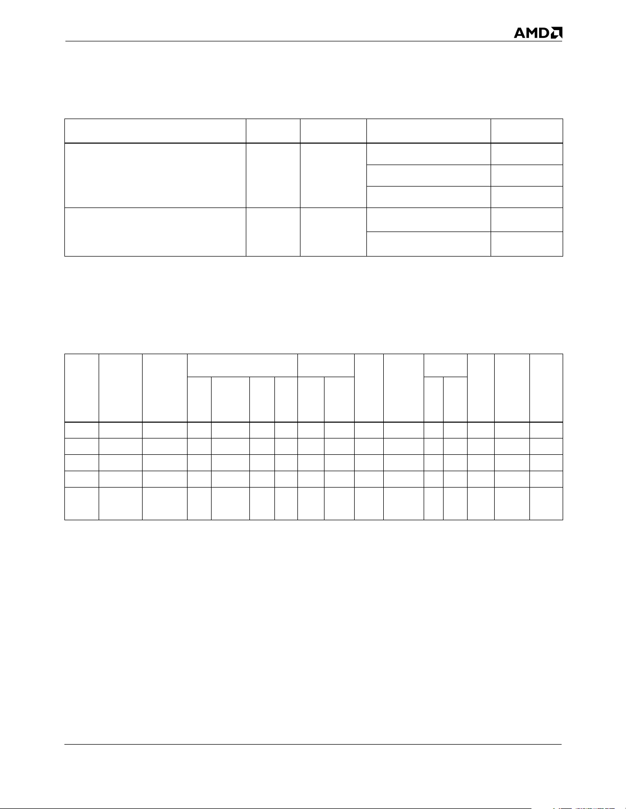
Table 1. Features of the AMD-K6™ Processor Family
Processor
AMD-K6E 7 0.25 6
AMD-K6-2 8/[7:0] 0.25 7 Yes
AMD-K6-2 and
AMD-K6-2E
AMD-K6-2E+ D/[7:4] 0.18
AMD-K6-III 9/[3:0] 0.25
AMD-K6-IIIE+ D/[3:0] 0.18
Notes:
1. Refer to “Model-Specific Registers Overview” on page 14 for more information.
2. Model 8/[F:8] defines the bits and fields in the Write Handling Control Register (WHCR) and Extended Feature Enable Register (EFER)
differently from the models 7 and 8/[7:0].
3. This model implements the same ten MSRs as the Model 8/[F:8]. With the exception of bit 4 (L2D) in the EFER register, the bits and
fields within these ten MSRs are defined identically.
4. Low-power versions implement one additional register to support AMD PowerNow!™ technology.
5. AMD PowerNow! technology is supported on low-power versions of these processors only.
Model/
Stepping
8/[F:8] 0.25
Process (in
microns)
Number
of MSRs
2
10
3,4
11
3
11
3,4
11
3DNow!™
1
Instructions
3DNow!
Extensions
Yes
Yes Yes
Yes
Yes Yes
AMD PowerNow!™
Technology
5
Yes
5
Yes
L2
Cache
128 Kbytes
256 Kbytes
The descriptions in the remainder of this section provide more
detailed information on the AMD-K6 processor family
members, and the models and steppings that comprise each
member.
Table 7 on page 14 and Table 8 on page 15 summarize the MSR
differences between the models and steppings of the AMD-K6
family of processors.
2 Processor Models and Steppings

Preliminary Information
23913A/0—November 2000 Embedded AMD-K6™ Processors BIOS Design Guide
AMD-K6™E Embedded Processor
Model 7 Model 7 is the first processor manufactured in the 0.25-micron
process.
■ Model 7 supports six model-specific registers (MSRs).
AMD-K6™-2 Processor
Some important features supported by the AMD-K6-2 processor
include the 3DNow!™ instruction set and a 100-MHz processor
bus.
Model 8/[7:0] Model 8/[7:0] is any of eight possible model/steppings—models
8/0, 8/1, 8/2, 8/3, 8/4, 8/5, 8/6, or 8/7. Model 8/[7:0] is
manufactured in the 0.25-micron process and was the original
version of the AMD-K6-2 available as a desktop product.
■ Model 8/[7:0] implements the same six MSRs as the Model 7,
and the bits and fields within these six MSRs are defined
identically.
■ Model 8/[7:0] also implements the SYSCALL/SYSRET
Target Address Register (STAR) MSR for a total of seven
MSRs.
Model 8/[F:8] Model 8/[F:8] is any of eight possible model/steppings—models
8/8, 8/9, 8/A, 8/B, 8/C, 8/D, 8/E, or 8/F. Model 8/[F:8] is
manufactured in the 0.25-micron process.
■ Model 8/[F:8] implements the same six MSRs as the models
7 and 8/[7:0], but the bits and fields within two of these
MSRs—WHCR and EFER—are not defined identically.
■ Also, Model 8/[F:8] supports the STAR MSR and three
additional MSRs, for a total of ten MSRs.
Processor Models and Steppings 3

Preliminary Information
Embedded AMD-K6™ Processors BIOS Design Guide 23913A/0—November 2000
AMD-K6™-2E Embedded Processor
The AMD-K6-2E processor also supports the 3DNow!
instruction set and a 100-MHz processor bus.
Model 8/[F:8] Model 8/[F:8] is any of eight possible model/steppings—models
8/8, 8/9, 8/A, 8/B, 8/C, 8/D, 8/E, or 8/F. Model 8/[F:8] is
manufactured in the 0.25-micron process.
■ Model 8/[F:8] implements the same six MSRs as the models
7 and 8/[7:0], but the bits and fields within two of these
MSRs—WHCR and EFER—are not defined identically.
■ Also, Model 8/[F:8] supports the STAR MSR and three
additional MSRs, for a total of ten MSRs.
AMD-K6™-2E+ Embedded Processor
In addition to supporting the 3DNow! instruction set and a 100MHz processor bus, the AMD-K6-2E+ processor contains a 128Kbyte backside L2 cache. It also supports the 3DNow! DSP
instructions extensions. Low-power versions of the processor
support AMD PowerNow!™ technology.
Model D/[7:4] Model D/[7:4] is any of four possible model/steppings—models
D/4, D/5, D/6, or D/7. Model D/[7:4] is manufactured in the 0.18micron process.
■ Model D/[7:4] implements the same ten MSRs as the Model
8/[F:8]. With the exception of bit 4 (L2D) in the EFER
register, the bits and fields within these ten MSRs are
defined identically for standard-power versions. The PSOR
register is defined differently for low-power versions.
■ Model D/[7:4] supports an additional MSR, the Level-2
Cache Array Access Register (L2AAR), for a total of eleven
MSRs.
■ Low-power versions of Model D/[7:4] support an additional
MSR, the Enhanced Power Management Register (EPMR),
for a total of twelve MSRs.
4 Processor Models and Steppings

Preliminary Information
23913A/0—November 2000 Embedded AMD-K6™ Processors BIOS Design Guide
AMD-K6™-III Processor
In addition to supporting the 3DNow! instruction set and a 100MHz processor bus, the AMD-K6-III processor contains a 256Kbyte backside L2 cache.
Model 9/[3:0] Model 9/[3:0] is any of four possible model/steppings—models
9/0, 9/1, 9/2, or 9/3. Model 9/[3:0] is manufactured in the 0.25micron process.
■ Model 9/[3:0] implements the same ten MSRs as the Model
8/[F:8]. With the exception of bit 4 (L2D) in the EFER
register, the bits and fields within these ten MSRs are
defined identically.
■ Model 9/[3:0] supports one additional MSR for a total of
eleven MSRs.
AMD-K6™-IIIE+ Embedded Processor
In addition to supporting the 3DNow! instruction set and a 100MHz processor bus, the AMD-K6-IIIE+ processor contains a 256Kbyte backside L2 cache. It also supports the 3DNow! DSP
instruction extensions. Low-power versions of the processor
support AMD PowerNow! technology.
Model D/[3:0] Model D/[3:0] is any of four possible model/steppings—models
D/0, D/1, D/2, or D/3. Model D/[3:0] is manufactured in the 0.18micron process.
■ Model D/[3:0] implements the same ten MSRs as the Model
8/[F:8]. With the exception of bit 4 (L2D) in the EFER
register, the bits and fields within these ten MSRs are
defined identically for standard-power versions. The PSOR
register is defined differently for low-power versions.
■ Model D/[7:4] supports an additional MSR, the Level-2
Cache Array Access Register (L2AAR), for a total of eleven
MSRs.
■ Low-power versions of Model D/[7:4] support an additional
MSR, the Enhanced Power Management Register (EPMR),
for a total of twelve MSRs.
Processor Models and Steppings 5

Preliminary Information
Embedded AMD-K6™ Processors BIOS Design Guide 23913A/0—November 2000
BIOS Consideration Checklist
CPUID
■ Use the CPUID instruction to properly identify the
processor. For information on the CPUID instruction, see
“CPUID Instruction Overview” on page 57.
■ Determine the processor model, stepping, and features
using functions 0000_0001h and 8000_0001h of the CPUID
instruction.
■ Display the processor name (BIOS boot strings) as described
in “CPUID Identification Algorithms” on page 11.
CPU Speed Detection
■ Use speed detection algorithms that do not rely on
repetitive instruction sequences.
■ Use the Time Stamp Counter (TSC) to ‘clock’ a timed
operation and compare the result to the real-time clock
(RTC) to determine the operating frequency. See the CPU
Speed Determination Program available on the AMD website
at http://www.amd.com/products/cpg/bin/.
■ Display the recommended BIOS boot string as shown in
Table 5 on page 11.
Model-Specific Registers (MSRs)
■ Only access MSRs implemented in the processor.
■ Enable write allocation by programming the Write Handling
Control Register (WHCR). See “Write Handling Control
Register (WHCR)” on page 19 and page 27, and the
Implementation of Write Allocate in the K86™ Processors
Application Note, order# 21326 for more information.
Note: The WHCR register as defined in models 7 and 8/[7:0] is
implemented differently in models 8/[F:8], 9, and D.
■ For the AMD-K6-2E, AMD-K6-2E+, AMD-K6-III, and
AMD-K6-IIIE+ processors, utilize the information provided
in the Processor State Observability Register (PSOR) to
display the correct processor bus frequency.
6 BIOS Consideration Checklist

Preliminary Information
23913A/0—November 2000 Embedded AMD-K6™ Processors BIOS Design Guide
Cache Testing
■ The AMD-K6 family of processors does not contain MSRs to
allow for testing of the L1 cache. However, the AMD-K6-2E+,
AMD-K6-III, and AMD-K6-IIIE+ processors do contain an
MSR that allows for testing of their L2 caches. This MSR is
called L2AAR, and it is described in “Level-2 Cache Array
Access Register (L2AAR)” on page 40.
SMM Issues
■ The System Management Mode (SMM) functionality of the
processor is the same as the Pentium® processor.
■ Implement the processor SMM state-save area in a similar
manner as Pentium processors except for the IDT Base and
possibly Pentium processor-reserved areas. See “System
Management Mode (SMM)” on page 13 for more
information.
BIOS Consideration Checklist 7
Preliminary Information
Embedded AMD-K6™ Processors BIOS Design Guide 23913A/0—November 2000
States after RESET and INIT
Register States after RESET and INIT
After the processor has completed its initialization following
the recognition of an asserted RESET or INIT signal, the states
of all architecture registers and MSRs are compatible with
those of Pentium processors. Differences are listed in Table 2
through Table 4.
Table 2. AMD-K6™E Processor (Model 7) and AMD-K6™ Processor (Model
8/[7:0]) State after RESET
Register RESET State
EDX
EFER 0000_0000_0000_0000h
2
STAR
WHCR 0000_0000_0000_0000h
0000_05MSh
0000_0000_0000_0000h
1
Notes:
1. “M” represents the Model and “S” represents the Stepping.
2. Processor Model 7 does not support the STAR register.
Table 3. AMD-K6™ Processor (Model 8/[F:8]) and AMD-K6™-2E Processor
(Model 8/[F:8]) State after RESET
Register RESET State
EDX
EFER 0000_0000_0000_0002h
PFIR 0000_0000_0000_0000h
PSOR
STAR 0000_0000_0000_0000h
UWCCR 0000_0000_0000_0000h
WHCR 0000_0000_0000_0000h
Notes:
1. “M” represents the Model and “S” represents the Stepping.
2. “B” represents PSOR[3:0], where PSOR[3] equals 0, and PSOR[2:0] is equal to the value of the
BF[2:0] signals sampled during the falling transition of RESET.
0000_05MSh
0000_0000_0000_01SBh
1
1,2
8 States after RESET and INIT
Preliminary Information
23913A/0—November 2000 Embedded AMD-K6™ Processors BIOS Design Guide
Table 4. AMD-K6™-2E+ (Model D), AMD-K6™-III (Model 9), and
AMD-K6™-IIIE+ Processors (Model D) State after RESET
Register RESET State
EDX
2
EFER
L2AAR 0000_0000_0000_0000h
PFIR 0000_0000_0000_0000h
PSOR
STAR 0000_0000_0000_0000h
UWCCR 0000_0000_0000_0000h
WHCR 0000_0000_0000_0000h
4
EPMR
0000_05MSh
0000_0000_0000_0002h
0000_0000_0000_00SBh
0000_0000_0000_0000h
1
1,3
Notes:
1. “M” represents the Model and “S” represents the Stepping.
2. Because EFER[4] equals 0 after RESET, the L2 cache is enabled by default after RESET.
3. “B” represents PSOR[3:0], where PSOR[3] equals 0, and PSOR[2:0] is equal to the value of the
BF[2:0] signals sampled during the falling transition of RESET.
4. Supported on low-power versions only of Model D processors.
Processor State after INIT
The assertion of INIT causes the processor to empty its
pipelines, initialize most of its internal state, and branch to
address FFFF_FFF0h—the same instruction execution starting
point used after RESET. Unlike RESET, the processor
preserves the contents of its caches, the floating-point state, the
SMM base, MSRs, and the CD and NW bits of the CR0 register.
The edge-sensitive interrupts FLUSH# and SMI# are sampled
and preserved during the INIT process and are handled
accordingly after the initialization is complete. However, the
processor resets any pending NMI interrupt upon sampling
INIT asserted.
INIT can be used as an accelerator for 80286 code that requires
a reset to exit from protected mode back to real mode.
States after RESET and INIT 9

Preliminary Information
Embedded AMD-K6™ Processors BIOS Design Guide 23913A/0—November 2000
Built-In Self-Test (BIST)
For all models of the AMD-K6 processor, BIST is run
unconditionally following the falling transition of RESET. The
results of the test are contained in the general-purpose register
EAX. If EAX contains 0000_0000h, then BIST was successful. If
the contents of EAX are non-zero, the BIST failed. The internal
resources tested during BIST include the following:
■ L1 instruction and data caches
■ L2 unified cache (models 9 and D only)
■ Instruction and data translation lookaside buffers (TLBs)
10 States after RESET and INIT
Preliminary Information
23913A/0—November 2000 Embedded AMD-K6™ Processors BIOS Design Guide
CPUID Identification Algorithms
The CPUID instruction provides information about the
processor (vendor, type, name, etc.) and its capabilities
(features). After detecting the processor and its capabilities,
software can be accurately tuned to the system for maximum
performance and benefit to users. For more detailed
information about using the CPUID instruction, see
“Embedded AMD Processor Recognition” on page 57.
To determine if the processor is enabled with AMD PowerNow!
technology, use CPUID function 8000_0007, as described on
page 79.
The recommended boot strings (or processor names) to be
displayed for AMD-K6 processors are shown in Table 5.
Table 5. Recommended Boot Strings for AMD-K6™ Processors
Model
Model 7 AMD-K6(tm)/XXX
All steppings of Models 8 AMD-K6(tm)-2/XXX
Model D/[7:4]
Model 9/[3:0] AMD-K6(tm)-III/XXX
Model D/[3:0]
Notes:
1. The value for XXX is determined by calculating the core frequency of the processor. Use the Time
Stamp Counter (TSC) to ‘clock’ a timed operation and compare the result to the real-time clock
(RTC) to determine the operating frequency.
2. See “Functions 8000_0002h, 8000_0003h, and 8000_0004h — Processor Name String” on page 77
for more information about these steppings.
2
2
Recommended Boot String Display
AMD-K6(tm)-2+/XXX
AMD-K6(tm)-III+/XXX
1
For example, a BIOS boot string for a Model 9, stepping 3, 450MHz AMD-K6-III processor would look like this:
■ AMD-K6(tm)-III/450
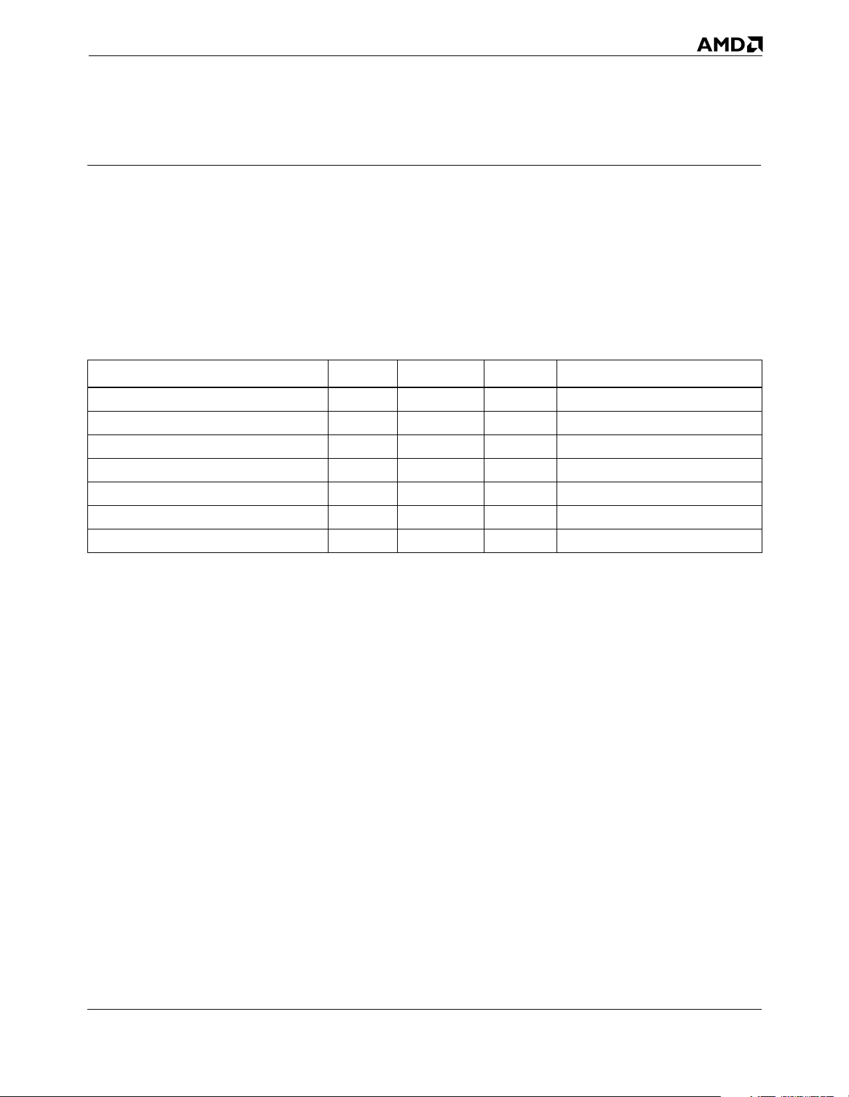
Figure 1 on page 12 shows a flow chart for the CPUID
instruction. Use this chart to implement a CPUID algorithm.
CPUID Identification Algorithms 11

Preliminary Information
Embedded AMD-K6™ Processors BIOS Design Guide 23913A/0—November 2000
Check for CPUID
instruction support
Execute CPUID
Extended Function
EAX=8000_0001h
CPUID instruction
supported
Yes
Execute CPUID
Standard Function EAX=0
Store Vendor String
EAX > 1 ?
Yes
Execute CPUID
Standard Function EAX=1
Store returned Standard
Function Feature bits and
Processor Signature;
Determine MMX and,
optionally, SSE* support
Execute CPUID
Extended Function
EAX=8000_0000h to
determine number of
extended functions supported
No
No
No CPUID instruction--
Use other means
to detect CPU type
AMD processor not
present—Check for
other CPU brands
Extended Functions
Not Supported
No
EAX >
8000_0001h ?
Yes
Utilize Vendor String and
Extended Function Feature
bits to determine 3DNow!,
3DNow! Extensions, and
MMX™ Extensions support
Utilize Processor Signature to
determine MSR support
Execute CPUID
Extended Functions
EAX=8000_0002h,
8000_0003h,
and 8000_0004h
to display processor
name string
Execute CPUID
Extended Functions
EAX=8000_0005h and
EAX=8000_0006h (Model 9 &
Model D) to gather processor
cache and TLB information
Execute CPUID
Extended Function
EAX=8000_0007h (Model D)
to gather AMD PowerNow!
technology information for t he
processor
Tune software to optimize
for features present
* Streaming SIMD Extensions
Done
Figure 1. CPUID Instruction Flow Chart
12 CPUID Identification Algorithms
Preliminary Information
23913A/0—November 2000 Embedded AMD-K6™ Processors BIOS Design Guide
System Management Mode (SMM)
This section documents the System Management Mode (SMM)
differences between specified models of the AMD-K6 processor
and the Pentium
implementation in the K86 processors, see the appropriate
AMD-K6 or AMD-K6E processor data sheet.
State-Save Map Differences
The SMM implemented in the AMD-K6 processor differs from
the SMM implemented in the Pentium® processor in one way.
The Interrupt Descriptor Table (IDT) base location in the
AMD-K6 processors is located at offset FF90h. The Pentium
processor has the IDT base located at offset FF94h.
processor. For more information on SMM
I/O Trap Dword Differences
The I/O trap dword is located at offset FFA4h. Its AMD-K6
processor bit fields are shown in Table 6. This state-save area,
which is reserved in Pentium processors, contains information
regarding an I/O instruction that may have been trapped by an
SMI# assertion.
Table 6. AMD-K6™ Processor I/O Trap Dword Configuration at Offset FFA4h
Bits 31–16 Bits 15–4 Bit 3 Bit 2 Bit 1 Bit 0
I/O Port Address Reserved Rep String Operation I/O String Operation Valid I/O Instruction Input or Output
System Management Mode (SMM) 13

Preliminary Information
Embedded AMD-K6™ Processors BIOS Design Guide 23913A/0—November 2000
Model-Specific Registers Overview
Each of the models of the AMD-K6 processor family support a
different set of model-specific registers (MSRs). These
differences are summarized by register in Table 7. The
differences are summarized by model in Table 8 on page 15,
where an ‘X’ indicates support for a register or field.
The content of ECX selects the MSR to be addressed by the
RDMSR and WRMSR instruction.
Table 7. Summary by Register of MSR Differences within the AMD-K6™ Family
Register Mnemonic ECX Value Models Description
Machine-Check Address Register MCAR 00h All page 16
Machine-Check Type Register MCTR 01h All page 16
Test Register 12 TR12 0Eh All page 16
Time Stamp Counter TSC 10h All page 16
7, 8/[7:0] page 18
Extended Feature Enable Register EFER C000_0080h
Write Handling Control Register WHCR C000_0082h
SYSCALL/SYSRET Target Address Register STAR C000_0081h
UC/WC Cacheability Control Register UWCCR C000_0085h
Processor State Observability Register PSOR C000_0087h
8/[F:8] page 24
9, D page 39
7, 8/[7:0] page 19
8/[F:8], 9, D page 27
7 Not supported
8, 9, D page 22
7, 8/[7:0] Not supported
8/[F:8], 9, D page 30
7, 8/[7:0] Not supported
8/[F:8], 9, D
1
page 34
Page Flush/Invalidate Register PFIR C000_0088h
2
D
7, 8/[7:0] Not supported
8/[F:8], 9, D page 36
page 46
14 Model-Specific Registers Overview
Preliminary Information
23913A/0—November 2000 Embedded AMD-K6™ Processors BIOS Design Guide
Table 7. Summary by Register of MSR Differences within the AMD-K6™ Family (continued)
Register Mnemonic ECX Value Models Description
7, 8 Not supported
Level-2 Cache Array Access Register L2AAR C000_0089h
9 page 40
D page 48
7, 8, 9, D
1
Enhanced Power Management Register EPMR C000_0086h
2
D
Notes:
1. Standard-power versions only.
2. Low-power versions only.
Table 8. Summary by Model of MSR Differences within the AMD-K6™ Family
2
EFER
Standard
Model Stepping
7 All X X X
8 7:0 X X X X
8 F:8 X X X X X X X X X
9 3:0 X X X X X X X X X X X
D
3:0
7:4
MSRs
L2D EWBEC DPE SCE
1
XXXXX XXX
508 MB4092
WHCR
3
MB
STAR UWCCR
PSOR
BF
4X5
X
PBF
VID
PFIR L2AAR EPMR
EBF
Not supported
page 54
XX
5
X
Notes:
1. There are four MSRs that every model and stepping of the AMD-K6 family of processors support identically—MCAR, MCTR, TR12, and
TSC.
2. L2D, EWBEC, and DPE are bits/fields supported in EFER for the indicated models/steppings. All models/steppings support the System
Call Extension (SCE) bit in EFER, even if the corresponding SYSCALL and SYSRET instructions and the STAR register are not supported.
3. Indicates whether the WAELIM field supports 508 Mbytes or 4092 Mbytes of memory. The location of the WAE15M bit and the WAELIM
field within the WHCR register differs between the models/steppings that support 508 Mbytes of memory and those that support 4092
Mbytes of memory.
4. Supported on standard-power versions only.
5. Supported on low-power versions only.
Model-Specific Registers Overview 15

Preliminary Information
Embedded AMD-K6™ Processors BIOS Design Guide 23913A/0—November 2000
Standard Model-Specific Registers (All Models)
This section describes the four standard MSRs that every model
and stepping of the AMD-K6 family of processors support
identically. See the appropriate AMD-K6 or AMD-K6E
processor data sheet for more detail on these standard
registers.
Machine-Check
Address Register
(MCAR) and
Machine-Check Type
Register (MCTR)
Test Register 12 (TR12)
Time Stamp Counter (TSC)
The processor does not support the generation of a machine
check exception, but does provide a 64-bit Machine Check
Address Register (MCAR) and a 64-bit Machine Check Type
Register (MCTR) for software compatibility. Because the
processor does not support machine check exceptions, the
contents of the MCAR and MCTR are only affected by the
WRMSR instruction and by RESET being sampled asserted
(where all bits in each register are reset to 0).
The processor also provides the Machine Check Exception
(MCE) bit in Control Register 4 (CR4, bit 6) as a read-write bit.
However, the state of this bit has no effect on the operation of
the processor.
The processor provides the 64-bit Test Register 12 (TR12), but
only the Cache Inhibit (CI) bit (bit 3 of TR12) is supported. All
other bits in TR12 have no effect on the processor’s operation.
Note: The I/O Trap Restart function (bit 9 of TR12) is always
enabled on AMD-K6 processors.
With each processor clock cycle, the processor increments a
64-bit time stamp counter (TSC) MSR. The counter can be
written or read using the WRMSR or RDMSR instructions when
the ECX register contains the value 10h and current privilege
level (CPL) = 0. The counter can also be read using the RDTSC
instruction, but the required privilege level for this instruction
is determined by the Time Stamp Disable (TSD) bit in CR4.
With either of these instructions, the EDX and EAX registers
hold the upper and lower dwords of the 64-bit value to be
written to or read from the TSC, as follows:
■ EDX—Upper 32 bits of TSC
■ EAX—Lower 32 bits of TSC
The TSC can be loaded with any arbitrary value. This feature is
compatible with the Pentium processor.
16 Model-Specific Registers Overview
Preliminary Information
23913A/0—November 2000 Embedded AMD-K6™ Processors BIOS Design Guide
Model 7 and Model 8/[7:0] Registers
The AMD-K6E processor Model 7 and the AMD-K6-2 processor
Model 8/[7:0] provide the model-specific registers listed in
Table 9.
The contents of ECX selects the MSR to be addressed by the
RDMSR and WRMSR instruction.
Table 9. Model-Specific Registers Supported by Models 7 and 8/[7:0]
Register Name Mnemonic ECX Value Description Comments
Machine-Check Address Register MCAR 00h page 16 Identical on all models
Machine-Check Type Register MCTR 01h page 16 Identical on all models
Test Register 12 TR12 0Eh page 16 Identical on all models
Time Stamp Counter TSC 10h page 16 Identical on all models
Extended Feature Enable Register EFER C000_0080h page 18
Write Handling Control Register WHCR C000_0082h page 19
SYSCALL/SYSRET Target Address Register STAR C000_0081h page 22 Not supported on Model 7
Model 7 and Model 8/[7:0] Registers 17

Preliminary Information
Embedded AMD-K6™ Processors BIOS Design Guide 23913A/0—November 2000
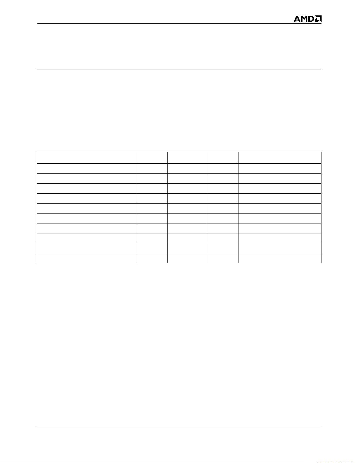
Extended Feature Enable Register (EFER)
The Extended Feature Enable Register (EFER) contains the
control bits that enable the extended features of the AMD-K6
processor. Figure 2 shows the format of the EFER register, and
Table 10 defines the function of each bit of the EFER register.
The EFER register is MSR C000_0080h.
1063
S
C
E
Reserved
Symbol Description Bit
SCE System Call Extension 0
Figure 2. Extended Feature Enable Register (EFER) (Models 7 and 8/[7:0])
Table 10. Extended Feature Enable Register (EFER) Definition (Models 7 and 8/[7:0])
Bit Description R/W Function
Writing a 1 to any reserved bit causes a general protection
63–1
Notes:
1. The AMD-K6E processor Model 7 provides the SCE bit in the EFER register, but this bit does not affect processor operation because the
SYSCALL and SYSRET instructions and the STAR register are not supported in this models.
Reserved
0
System Call Extension (SCE)
1
R
fault to occur. All reserved bits are always read as 0.
SCE must be set to 1 to enable the usage of the SYSCALL and
R/W
SYSRET instructions.
18 Model 7 and Model 8/[7:0] Registers

Preliminary Information
23913A/0—November 2000 Embedded AMD-K6™ Processors BIOS Design Guide
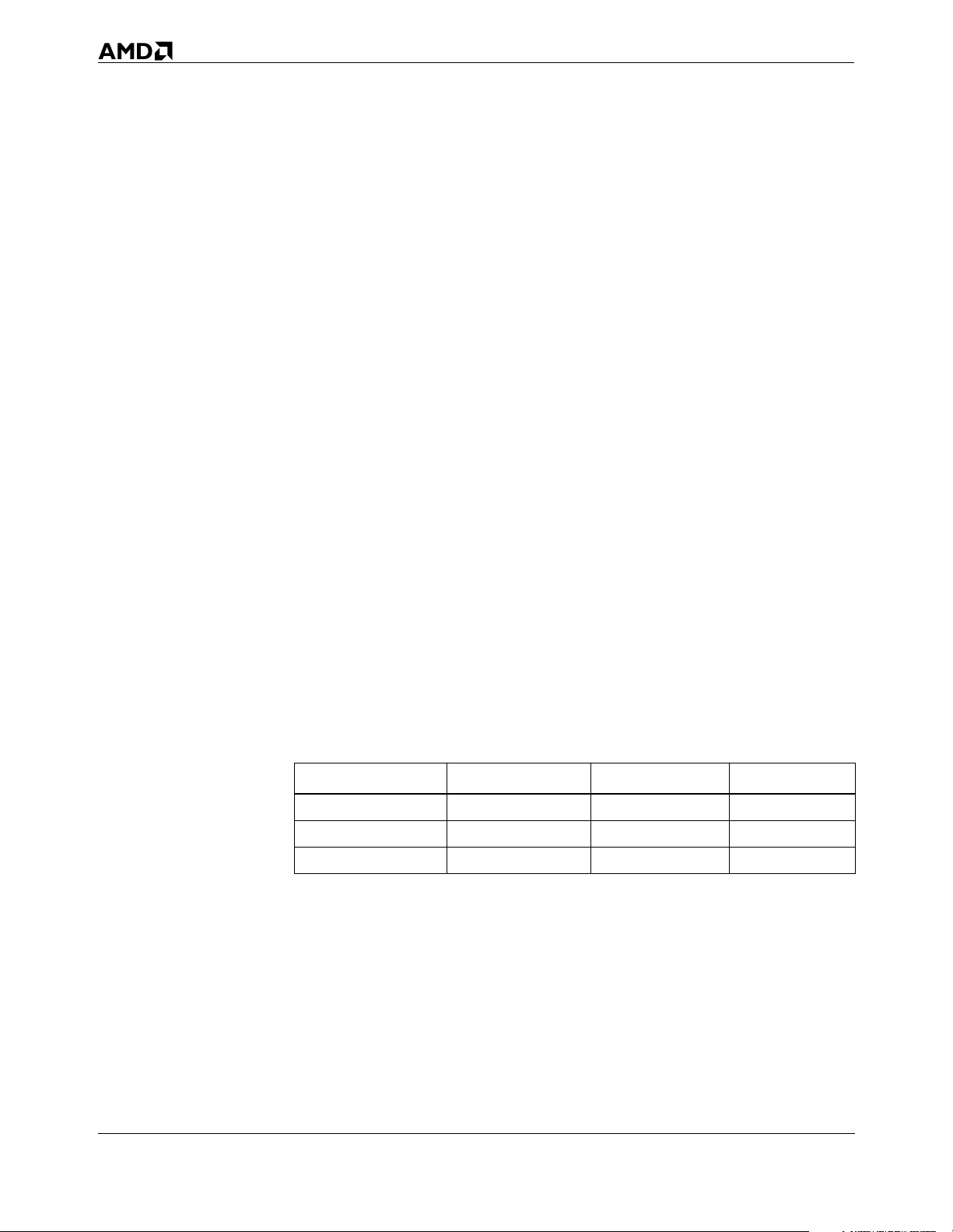
Write Handling Control Register (WHCR)
The Write Handling Control Register (WHCR) (see Figure 3 on
page 20) is an MSR that contains three fields—the Write
Cacheability Detection Enable (WCDE) bit, the Write Allocate
Enable Limit (WAELIM) field, and the Write Allocate Enable
15-to-16-Mbyte (WAE15M) bit. The WHCR register is MSR
C000_0082h.
AMD-K6 processors contain a split level-1 (L1) 64-Kbyte
writeback cache organized as a separate 32-Kbyte instruction
cache and a 32-Kbyte data cache with two-way set associativity.
The cache line size is 32 bytes and lines are read from memory
using an efficient pipelined burst read cycle. Further
performance gains are achieved by the implementation of a
write allocation scheme.
Write Allocation A write allocate, if enabled, occurs when the processor has a
pending memory write cycle to a cacheable line and the line
does not currently reside in the L1 cache. For more information,
see the Implementation of Write Allocate in the K86™ Processors
Application Note, order# 21326, and the “Cache Organization”
chapter in the appropriate AMD-K6 or AMD-K6E processor
data sheet.
This section describes two programmable mechanisms used by
the processor to determine when to perform write allocate.
When either of these mechanisms indicates that a pending
write is to a cacheable area of memory, a write allocate is
performed.
Before enabling write allocate or changing memory
cacheability/writeability, the BIOS must writeback and
invalidate the internal cache by using the WBINVD instruction.
In addition, write allocate should be enabled only after
performing any memory sizing or typing algorithms.
Model 7 and Model 8/[7:0] Registers 19
Preliminary Information
Embedded AMD-K6™ Processors BIOS Design Guide 23913A/0—November 2000
9
71063
8
W
A
E
1
5
M
Reserved
Symbol Description Bits
WCDE Always program to 0 8
WAELIM Write Allocate Enable Limit 7–1
WAE15M Write Allocate Enable 15-to-16-Mbyte 0
Note: Hardware RESET initializes this MSR to all zeros.
0
WAELIM
Figure 3. Write Handling Control Register (WHCR) (Models 7 and 8/[7:0])
Write Cacheability Detection Enable Bit
Write Allocate Enable Limit Field
For proper functionality, always program bit 8 of WHCR to 0.
See “Pipelining Support” on page 69 for more information on
the WCDE bit.
The WAELIM field is 7 bits wide. This field, multiplied by 4
Mbytes, defines an upper memory limit. Any pending write
cycle that misses the L1 cache and that addresses memory
below this limit causes the processor to perform a write
allocate (assuming the address is not within a range where
write allocates are disallowed).
Write allocate is disabled for memory accesses at and above
this limit unless the processor determines a pending write
cycle is cacheable by means of one of the other write allocate
mechanisms—“Write to a Cacheable Page” and “Write to a
Sector” (for more information, see the “Cache Organization”
chapter in the appropriate AMD-K6 or AMD-K6E processor
data sheet.
7
The maximum value of this limit is ((2
–1) · 4 Mbytes) = 508
Mbytes. When all the bits in this field are set to 0, all memory
is above this limit and the write allocate mechanism is
disabled (even if all bits in the WAELIM field are set to 0,
write allocates can still occur due to the “Write to a Cacheable
Page” and “Write to a Sector” mechanisms).
Once the BIOS determines the amount of RAM installed in the
system, this number should also be used to program the
WAELIM field. For example, a system with 32 Mbytes of RAM
would program the WAELIM field with the value 0001000b.
20 Model 7 and Model 8/[7:0] Registers

Preliminary Information
23913A/0—November 2000 Embedded AMD-K6™ Processors BIOS Design Guide
This value (8), when multiplied by 4 Mbytes, yields 32 Mbytes
as the write allocate limit.
Write Allocate Enable
15-to-16-Mbyte Field.
The WAE15M bit is used to enable write allocations for the
memory write cycles that address the 1 Mbyte of memory
between 15 Mbytes and 16 Mbytes. This bit must be set to 1 to
allow write allocates in this memory area.
This sub-mechanism of the WAELIM provides a memory hole to
prevent write allocates. This memory hole is provided to
account for a small number of uncommon memory-mapped I/O
adapters that use this particular memory address space. If the
system contains one of these peripherals, the bit should be set
to 0 (even if the WAE15M bit is set to 0, write allocates can still
occur between 15 Mbytes and 16 Mbytes due to the “Write to a
Cacheable Page” and “Write to a Sector” mechanisms). The
WAE15M bit is ignored if the value in the WAELIM field is set
to less than 16 Mbytes.
By definition, write allocations are not performed in the
memory area between 640 Kbytes and 1 Mbyte unless the
processor determines a pending write cycle is cacheable by
means of “Write to a Cacheable Page” or “Write to a Sector.” It
is not safe to perform write allocations between 640 Kbytes and
1 Mbyte (000A_0000h to 000F_FFFFh) because it is considered
a noncacheable region of memory.
Model 7 and Model 8/[7:0] Registers 21
Preliminary Information
Embedded AMD-K6™ Processors BIOS Design Guide 23913A/0—November 2000
SYSCALL/SYSRET Target Address Register (STAR)
Models 8, 9, and D implement the STAR register. This register
contains the target EIP address used by the SYSCALL
instruction and the 16-bit code and stack segment selector
bases used by the SYSCALL and SYSRET instructions.
Figure 4 shows the format of the STAR register, and Table 11
defines the function of each field of the STAR register. The
STAR register is MSR C000_0081h.
For more information about SYSCALL/SYSRET, see the
SYSCALL and SYSRET Instruction Specification Application Note,
order# 21086.
31 063
32
Target EIP Address
SYSRET CS Selector and SS
Selector Base
47
48
SYSCALL CS Selector and SS
Selector Base
Figure 4. SYSCALL/SYSRET Target Address Register (STAR) (Models 8, 9, and D)
Table 11. SYSCALL/SYSRET Target Address Register (STAR) Definition (Models 8, 9, and D)
Bit Description R/W Function
During the SYSRET instruction, this field is copied into the CS
63–48
47–32
31–0
SYSRET CS and SS Selector Base
SYSCALL CS and SS Selector Base
Target EIP Address
R/W
register and the contents of this field, plus 1000b, are copied
into the SS register.
During the SYSCALL instruction, this field is copied into the
R/W
CS register and the contents of this field, plus 1000b, are
copied into the SS register.
During the SYSCALL instruction, this address is copied into
R/W
the EIP and points to the new starting address.
22 Model 7 and Model 8/[7:0] Registers
Preliminary Information
23913A/0—November 2000 Embedded AMD-K6™ Processors BIOS Design Guide
Model 8/[F:8] Registers
The AMD-K6-2 processor Model 8/[F:8] and AMD-K6-2E
processor Model 8/[F:8] provides the ten MSRs listed in Table
12.
The contents of ECX select the MSR to be addressed by the
RDMSR and WRMSR instruction.
Table 12. Model-Specific Registers Supported by Model 8/[F:8]
Register Name Mnemonic ECX Value Description Comments
Machine-Check Address Register MCAR 00h page 16 Identical on all models
Machine-Check Type Register MCTR 01h page 16 Identical on all models
Test Register 12 TR12 0Eh page 16 Identical on all models
Time Stamp Counter TSC 10h page 16 Identical on all models
Extended Feature Enable Register EFER C000_0080h page 24 Newly defined for Model 8/[F:8]
Write Handling Control Register WHCR C000_0082h page 27 Newly defined for Model 8/[F:8]
SYSCALL/SYSRET Target Address Register STAR C000_0081h page 22 Identical to Model 8/[7:0]
UC/WC Cacheability Control Register UWCCR C000_0085h page 30 New for Model 8/[F:8]
Processor State Observability Register PSOR C000_0087h page 34 New for Model 8/[F:8]
Page Flush/Invalidate Register PFIR C000_0088h page 36 New for Model 8/[F:8]
Model 8/[F:8] Registers 23

Preliminary Information
Embedded AMD-K6™ Processors BIOS Design Guide 23913A/0—November 2000
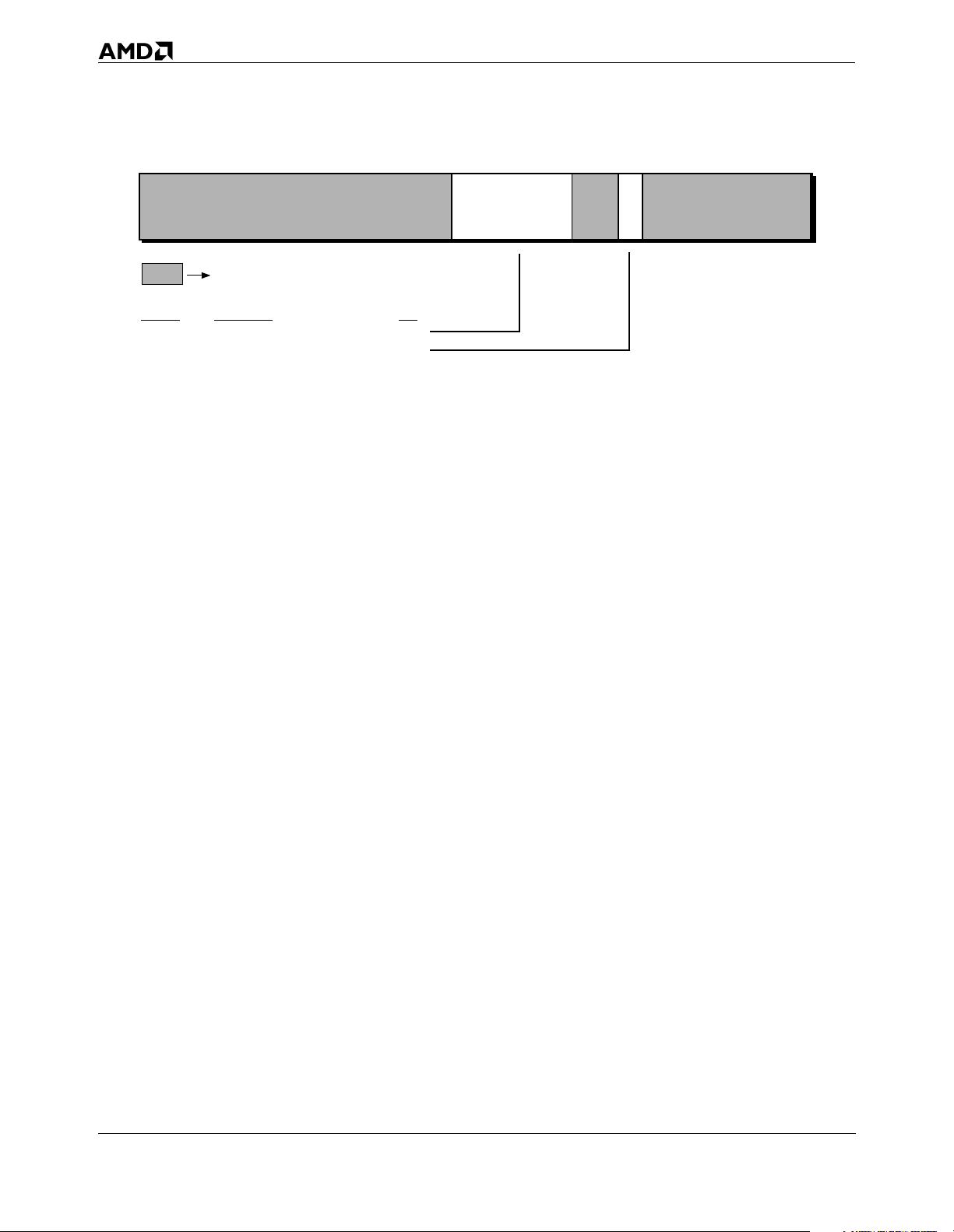
Extended Feature Enable Register (EFER)
The Extended Feature Enable Register (EFER) contains the
control bits that enable the extended features of the processor.
Figure 5 shows the format of the EFER register, and Table 13
defines the function of each bit of the EFER register. The EFER
register is MSR C000_0080h.
Note: The EFER register as defined in models 7 and 8/[7:0] is
defined differently in Model 8/[F:8]. A complete description
of the newly defined register is included in this section for
Model 8/[F:8].
1063
234
S
EWBEC
D
C
P
E
E
Reserved
Symbol Description Bit
EWBEC EWBE Control 3-2
DPE Data Prefetch Enable 1
SCE System Call Extension 0
Figure 5. Extended Feature Enable Register (EFER) (Model 8/[F:8])
Table 13. Extended Feature Enable Register (EFER) Definition (Model 8/[F:8])
Bit Description R/W Function
Writing a 1 to any reserved bit causes a general protection
63–4
3-2
1
0
Reserved
EWBE# Control (EWBEC)
Data Prefetch Enable (DPE)
System Call Extension (SCE)
R
fault to occur. All reserved bits are always read as 0.
This 2-bit field controls the behavior of the processor with
respect to the ordering of write cycles and the EWBE# signal.
R/W
EFER[3] and EFER[2] are Global EWBE# Disable (GEWBED)
and Speculative EWBE Disable (SEWBED), respectively.
DPE must be set to 1 to enable data prefetching (this is the
default setting following reset). If enabled, cache misses initi-
R/W
ated by a memory read within a 32-byte cache line are conditionally followed by cache-line fetches of the other line in
the 64-byte sector.
SCE must be set to 1 to enable the usage of the SYSCALL and
R/W
SYSRET instructions.
External Write Buffer Empty Control Field
Model 8/[F:8] contains an 8-byte write merge buffer that allows
the processor to conditionally combine data from multiple
noncacheable write cycles into this merge buffer. The merge
24 Model 8/[F:8] Registers

Preliminary Information
23913A/0—November 2000 Embedded AMD-K6™ Processors BIOS Design Guide
buffer operates in conjunction with the Memory Type Range
Registers (MTRRs). Refer to “UC/WC Cacheability Control
Register (UWCCR)” on page 30 for a description of the MTRRs.
Merging multiple write cycles into a single write cycle reduces
processor bus utilization and processor stalls, thereby
increasing the overall system performance.
Out-of-Order Write Cycles. The presence of the merge buffer
creates the potential to perform out-of-order write cycles
relative to the processor’s cache. In general, the ordering of
write cycles that are driven externally on the system bus and
those that hit the processor’s cache can be controlled by the
EWBE# signal. If EWBE# is sampled negated, the processor
delays the commitment of write cycles to cache lines in the
modified state or exclusive state in the processor’s cache.
Therefore, the system logic can enforce strong ordering by
negating EWBE# until the external write cycle is complete,
thereby ensuring that a subsequent write cycle that hits the
cache does not complete ahead of the external write cycle.
However, the addition of the write merge buffer introduces the
potential for out-of-order write cycles to occur between writes
to the merge buffer and writes to the processor’s cache. Because
these writes occur entirely within the processor and are not
sent out to the processor bus, the system logic is not able to
enforce strong ordering with the EWBE# signal.
The EWBE# control (EWBEC) bits provide a mechanism for
enforcing three different levels of write ordering in the
presence of the write merge buffer:
Best Performance. EFER[3] is defined as the Global EWBE#
Disable (GEWBED). When GEWBED equals 1, the processor
does not attempt to enforce any write ordering internally or
externally (the EWBE# signal is ignored). This is the maximum
performance setting.
Close-to-Best Performance. EFER[2] is defined as the Speculative
EWBE# Disable (SEWBED). SEWBED only affects the
processor when GEWBED equals 0. If GEWBED equals 0 and
SEWBED equals 1, the processor enforces strong ordering for
all internal write cycles with the exception of write cycles
addressed to a range of memory defined as uncacheable (UC) or
write-combining (WC) by the MTRRs. In addition, the processor
Model 8/[F:8] Registers 25
Preliminary Information
Embedded AMD-K6™ Processors BIOS Design Guide 23913A/0—November 2000
samples the EWBE# signal. If EWBE# is sampled negated, the
processor delays the commitment of write cycles to processor
cache lines in the modified state or exclusive state until EWBE#
is sampled asserted.
This setting provides performance comparable to, but slightly
less than, the performance obtained when GEWBED equals 1
because some degree of write ordering is maintained.
Slowest Performance. If GEWBED equals 0 and SEWBED equals 0,
the processor enforces strong ordering for all internal and
external write cycles. In this setting, the processor assumes, or
speculates, that strong order must be maintained between writes
to the merge buffer and writes that hit the processor’s cache.
Once the merge buffer is written out to the processor’s bus, the
EWBE# signal is sampled. If EWBE# is sampled negated, the
processor delays the commitment of write cycles to processor
cache lines in the modified state or exclusive state until EWBE#
is sampled asserted.
This setting is the default after RESET and provides the lowest
performance of the three settings because full write ordering is
maintained.
Write Ordering and Performance. Table 14 summarizes the three
settings of the EWBEC field, along with the effect of write
ordering and performance.
Table 14. Write Ordering and Performance Settings for EFER Register
EFER[3] (GEWBED) EFER[2] (SEWBED) Write Ordering Performance
1 0 or 1
01
0 (Default) 0 (Default)
None Best
All except UC/WC Close-to-Best
All Slowest
Enforcing complete write ordering in a uniprocessor system is
usually not necessary. In order to achieve the highest level of
performance while still maintaining support for the EWBE#
signal, AMD recommends that the BIOS set EFER[3:2] to 01b
(close-to-best performance). Many uniprocessor systems do not
support the EWBE# signal, in which case AMD recommends
that the BIOS set EFER[3:2] to 10b or 11b (best performance).
26 Model 8/[F:8] Registers

Preliminary Information
23913A/0—November 2000 Embedded AMD-K6™ Processors BIOS Design Guide
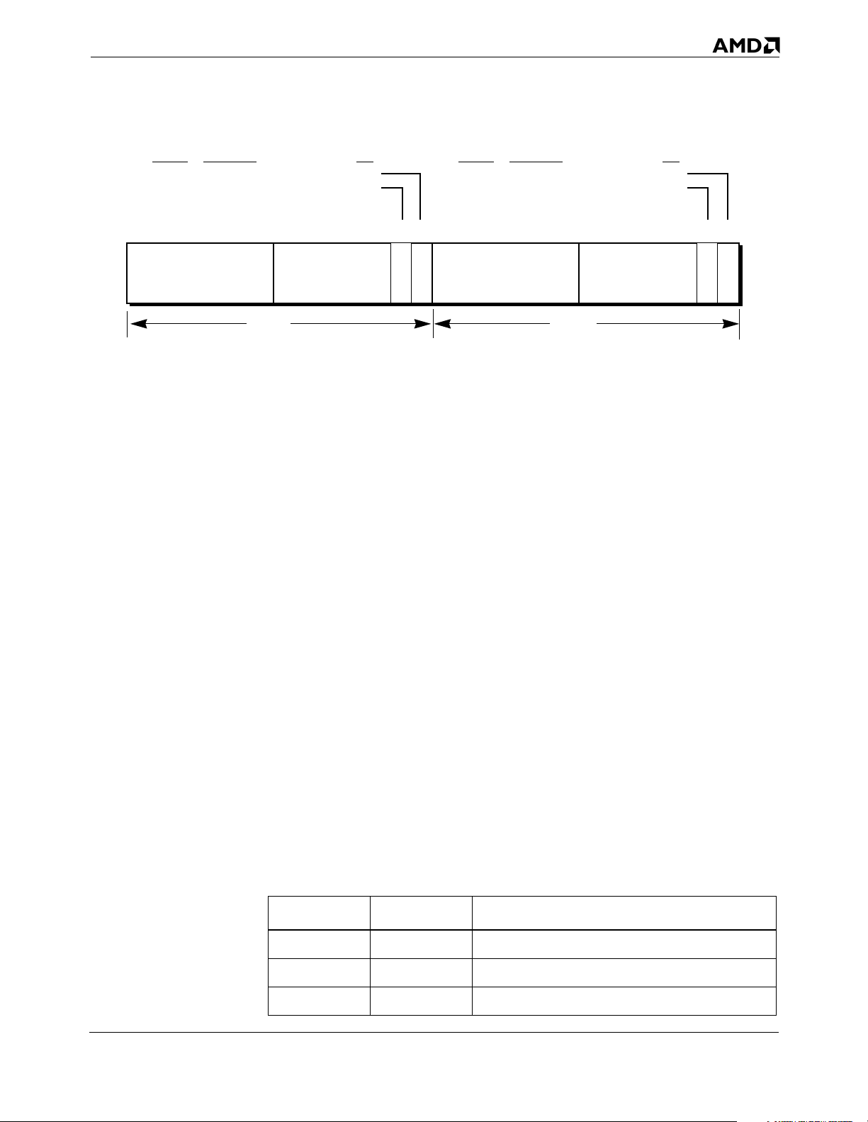
Write Handling Control Register (WHCR)
The Write Handling Control Register (WHCR) (see Figure 6 on
page 28) is an MSR that contains two fields—the Write Allocate
Enable Limit (WAELIM) field and the Write Allocate Enable
15-to-16-Mbyte (WAE15M) bit. The WHCR register is MSR
C000_0082h.
Note: The WHCR register as defined in the models 7 and 8/[7:0] is
defined differently in models 8/[F:8], 9, and D. A complete
description of the newly defined register is included in this
section for models 8/[F:8], 9, and D.
AMD-K6 processors contain a split level-1 (L1) 64-Kbyte
writeback cache organized as a separate 32-Kbyte instruction
cache and a 32-Kbyte data cache with two-way set associativity.
The cache line size is 32 bytes, and lines are read from memory
using an efficient pipelined burst read cycle. Further
performance gains are achieved by the implementation of a
write allocation scheme.
Write Allocation A write allocate, if enabled, occurs when the processor has a
pending memory write cycle to a cacheable line and the line
does not currently reside in the L1 cache. For more information
on write allocate, see the Implementation of Write Allocate in the
K86™ Processors Application Note, order# 21326 and see the
“Cache Organization” chapter in the appropriate AMD-K6 or
AMD-K6E processor data sheet.
This section describes two programmable mechanisms used by
the processor to determine when to perform write allocate.
When either of these mechanisms indicates that a pending
write is to a cacheable area of memory, a write allocate is
performed.
Before enabling write allocate or changing memory
cacheability, the BIOS must write back and invalidate the
internal cache by using the WBINVD instruction. In addition,
write allocate should be enabled only after performing any
memory sizing or typing algorithms.
Model 8/[F:8] Registers 27
Preliminary Information
Embedded AMD-K6™ Processors BIOS Design Guide 23913A/0—November 2000
16
17
213132
WAELIM
Reserved
Symbol Description Bits
WAELIM Write Allocate Enable Limit 31-22
WAE15M Write Allocate Enable 15-to-16-Mbyte 16
Note: Hardware RESET initializes this MSR to all zeros.
1522 063
W
A
E
1
5
M
Figure 6. Write Handling Control Register (WHCR) (Models 8/[F:8], 9, and D)
Write Allocate Enable Limit Field
The WAELIM field is 10 bits wide. This field, multiplied by 4
Mbytes, defines an upper memory limit. Any pending write
cycle that misses the L1 cache and that addresses memory
below this limit causes the processor to perform a write allocate
(assuming the address is not within a range where write
allocates are disallowed).
Write allocate is disabled for memory accesses at and above this
limit unless the processor determines a pending write cycle is
cacheable by means of one of the other write allocate
mechanisms—“Write to a Cacheable Page” and “Write to a
Sector” (for more information, see the “Cache Organization”
chapter in the appropriate AMD-K6 or AMD-K6E processor
data sheet.
10
The maximum value of this limit is ((2
–1) · 4 Mbytes) = 4092
Mbytes. When all the bits in this field are set to 0, all memory is
above this limit and the write allocate mechanism is disabled
(even if all bits in the WAELIM field are set to 0, write allocates
can still occur due to the “Write to a Cacheable Page” and
“Write to a Sector” mechanisms).
Once the BIOS determines the amount of RAM installed in the
system, this number should also be used to program the
WAELIM field. For example, a system with 32 Mbytes of RAM
would program the WAELIM field with the value
00_0000_1000b. This value (8), when multiplied by 4 Mbytes,
yields 32 Mbytes as the write allocate limit.
28 Model 8/[F:8] Registers

Preliminary Information
23913A/0—November 2000 Embedded AMD-K6™ Processors BIOS Design Guide
Write Allocate Enable
15-to-16-Mbyte Field
The WAE15M bit is used to enable write allocations for the
memory write cycles that address the 1 Mbyte of memory
between 15 Mbytes and 16 Mbytes. This bit must be set to 1 to
allow write allocates in this memory area.
This sub-mechanism of the WAELIM provides a memory hole to
prevent write allocates. This memory hole is provided to
account for a small number of uncommon memory-mapped I/O
adapters that use this particular memory address space. If the
system contains one of these peripherals, the bit should be set
to 0 (even if the WAE15M bit is set to 0, write allocates can still
occur between 15 Mbytes and 16 Mbytes due to the “Write to a
Cacheable Page” and “Write to a Sector” mechanisms). The
WAE15M bit is ignored if the value in the WAELIM field is set
to less than 16 Mbytes.
By definition, write allocations are not performed in the
memory area between 640 Kbytes and 1 Mbyte unless the
processor determines a pending write cycle is cacheable by
means of “Write to a Cacheable Page” or “Write to a Sector.” It
is not safe to perform write allocations between 640 Kbytes and
1 Mbyte (000A_0000h to 000F_FFFFh) because it is considered
a noncacheable region of memory. Additionally, if a memory
region is defined as write-combinable or uncacheable by a
MTRR, write allocates are not performed in that region.
Model 8/[F:8] Registers 29

Preliminary Information
Embedded AMD-K6™ Processors BIOS Design Guide 23913A/0—November 2000
UC/WC Cacheability Control Register (UWCCR)
Models 8/[F:8], 9, and D provide two variable-range Memory
Type Range Registers (MTRRs)—MTRR0 and MTRR1—that
each specify a range of memory. Each range can be defined as
one of the following memory types:
■ Uncacheable (UC) Memory—Memory read cycles are sourced
directly from the specified memory address, and the
processor does not allocate a cache line. Memory write
cycles are targeted at the specified memory address, and a
write allocation does not occur.
■ Write-Combining (WC) Memory—Memory read cycles are
sourced directly from the specified memory address, and the
processor does not allocate a cache line. The processor
conditionally combines data from multiple noncacheable
write cycles that are addressed within this range into a
merge buffer. Merging multiple write cycles into a single
write cycle reduces processor bus utilization and processor
stalls, thereby increasing the overall system performance.
This memory type is applicable for linear video frame
buffers.
Note: The MTRRs defined in this document are not software-
compatible to the MTRRs defined by the Pentium Pro and
Pentium II processors.
The programmer accesses the MTRRs by addressing the 64-bit
MSR known as the UC/WC Cacheability Control Register
(UWCCR). The MSR address of the UWCCR is C000_0085h.
Following reset, all bits in the UWCCR register are set to 0.
MTRR0 (lower 32 bits of the UWCCR register) defines the size
and memory type of range 0 and MTRR1 (upper 32 bits) defines
the size and memory type of range 1 (see Figure 7 on page 31).
Prior to programming write-combining or uncacheable areas of
memory in the UWCCR, the software must disable the
processor’s cache, then flush the cache. This can be achieved by
setting the CD bit in CR0 to 1 and executing the WBINVD
instruction. Following the programming of the UWCCR, the
processor’s cache must be enabled by setting the CD bit in CR0
to 0.
30 Model 8/[F:8] Registers
Preliminary Information
23913A/0—November 2000 Embedded AMD-K6™ Processors BIOS Design Guide
Symbol Description Bits
UC1 Uncacheable Memory Type 32
WC1 Write-Combining Memory Type 33
Physical Address Mask 1Physical Base Address 1
MTRR1 MTRR0
W
C
1
Symbol Description Bits
UC0 Uncacheable Memory Type 0
WC0 Write-Combining Memory Type 1
3233344849
U
Physical Base Address 0
C
1
1731
16 063
Physical Address Mask 0
Figure 7. UC/WC Cacheability Control Register (UWCCR) (Models 8/[F:8], 9, and D)
Physical Base
Address n (n=0, 1)
This address is the 15 most-significant bits of the physical base
address of the memory range. The least-significant 17 bits of the
base address are not needed because the base address is by
definition always aligned on a 128-Kbyte boundary.
Physical Address
Mask n (n=0, 1)
This value is the 15 most-significant bits of a physical address
mask that is used to define the size of the memory range. This
mask is logically ANDed with both the physical base address
field of the UWCCR register and the physical address
generated by the processor. If the results of the two AND
operations are equal, then the generated physical address is
considered within the range. That is, if:
12
U
W
C
C
0
0
Mask & Physical Base Address = Mask & Physical Address Generated
then, the physical address generated by the processor is in the
range.
WCn (n=0, 1) When set to 1, this memory range is defined as write-
combinable (refer to Table 15). Write-combinable memory is
uncacheable.
UCn (n=0, 1) When set to 1, this memory range is defined as uncacheable
(refer to Table 15).
Table 15. WC/UC Memory Type for UWCCR Register
WCn UCn Memory Type
0 0 No effect on cacheability or write-combining
1 0 Write-combining memory range (uncacheable)
0 or 1 1 Uncacheable memory range
Model 8/[F:8] Registers 31

Preliminary Information
Embedded AMD-K6™ Processors BIOS Design Guide 23913A/0—November 2000
Memory-Range Restrictions
The following rules regarding the address alignment and size of
each range must be adhered to when programming the physical
base address and physical address mask fields of the UWCCR
register:
■ The minimum size of each range is 128 Kbytes.
■ The physical base address must be aligned on a 128-Kbyte
boundary.
■ The physical base address must be range-size aligned. For
example, if the size of the range is 1 Mbyte, then the
physical base address must be aligned on a 1-Mbyte
boundary.
■ All bits set to 1 in the physical address mask must be
contiguous. Likewise, all bits set to 0 in the physical address
mask must be contiguous. For example:
111_1111_1100_0000b is a valid physical address mask.
111_1111_1101_0000b is invalid.
Table 16 lists the valid physical address masks and the resulting
range sizes that can be programmed in the UWCCR register.
Table 16. Valid Masks and Range Sizes for UWCCR Register
Masks Size
111_1111_1111_1111b 128 Kby tes
111_1111_1111_1110b 256 Kby tes
111_1111_1111_1100b 512 Kbytes
111_1111_1111_1000b 1 Mbyte
111_1111_1111_0000b 2 Mbytes
111_1111_1110_0000b 4 Mbytes
111_1111_1100_0000b 8 Mbytes
111_1111_1000_0000b 16 Mbytes
111_1111_0000_0000b 32 Mbytes
111_1110_0000_0000b 64 Mbytes
111_1100_0000_0000b 128 Mbytes
111_1000_0000_0000b 256 Mbytes
111_0000_0000_0000b 512 Mbytes
110_0000_0000_0000b 1 Gbyte
100_0000_0000_0000b 2 Gbytes
000_0000_0000_0000b 4 Gbytes
32 Model 8/[F:8] Registers

Preliminary Information
23913A/0—November 2000 Embedded AMD-K6™ Processors BIOS Design Guide
Examples Suppose that the range of memory from 16 Mbytes to 32 Mbytes
is uncacheable, and the 8-Mbyte range of memory on top of 1
Gbyte is write-combinable. Range 0 is defined as the
uncacheable range, and range 1 is defined as the writecombining range.
■ Extracting the 15 most-significant bits of the 32-bit physical
base address that corresponds to 16 Mbytes (0100_0000h)
yields a physical base address 0 field of
000_0000_1000_0000b. Because the uncacheable range size
is 16 Mbytes, the physical mask value 0 field is
111_1111_1000_0000b, according to Table 16 on page 32. Bit
1 of the UWCCR register (WC0) is set to 0, and bit 0 of the
UWCCR register is set to 1 (UC0).
■ Extracting the 15 most-significant bits of the 32-bit physical
base address that corresponds to 1 Gbyte (4000_0000h)
yields a physical base address 1 field of
010_0000_0000_0000b. Because the write-combining range
size is 8 Mbytes, the physical mask value 1 field is
111_1111_1100_0000b, according to Table 16. Bit 33 of the
UWCCR register (WC1) is set to 1 and bit 32 of the UWCCR
register is set to 0 (UC1).
Model 8/[F:8] Registers 33

Preliminary Information
Embedded AMD-K6™ Processors BIOS Design Guide 23913A/0—November 2000
Processor State Observability Register (PSOR)
Models 8/[F:8], 9, and standard-power versions of Model D
provide the Processor State Observability Register (PSOR) as
defined in Figure 8. The PSOR register is MSR C000_0087h.
Note: See page 46 for definitions of the PSOR bit fields for low-
power Model D processors.
.
20
63
Reserved
Symbol Description Bit
NOL2 No L2 Functionality 8
STEP Processor Stepping 7-4
BF Bus Frequency Divisor 2-0
789
N
O
STEP
L
2
34
BF
Figure 8. Processor State Observability Register (PSOR) (Models 8/[F:8], 9, and Standard-Power D)
NOL2 Bit This read-only bit indicates whether the processor contains an
L2 cache.
Note: This bit is always set to 1 for Model 8/[F:8].
Note: This bit is always set to 0 for Models 9 and D.
STEP Field This read-only field contains the stepping ID. This is identical to
the value returned by the CPUID standard function 1 in
EAX[3:0].
BF Field This read-only field contains the value of the BF signals
sampled by the processor during the falling transition of
RESET, which allows the BIOS to determine the frequency of
the host bus.
■ The core frequency must first be known, which can be
determined using the Time Stamp Counter method (See
“Time Stamp Counter (TSC)” on page 16).
■ The core frequency is then divided by the processor-clock to
bus-clock ratio as determined by the BF field of the PSOR
register (see Table 17 and Table 18 on page 35).
■ The result is the frequency of the processor bus.
34 Model 8/[F:8] Registers

Preliminary Information
23913A/0—November 2000 Embedded AMD-K6™ Processors BIOS Design Guide
Table 17. Processor-to-Bus Clock Ratios (Models 8/[F:8] and 9)
State of BF[2:0] Processor-Clock to Bus-Clock Ratio
100b 2.5x
101b 3.0x
110b 6.0x
111b 3.5x
000b 4.5x
001b 5.0x
010b 4.0x
011b 5.5x
Notes:
1. The 2.0x ratio that is supported on models 7 and 8/[7:0] is not supported on models 8/[F:8] or 9.
Instead, if BF[2:0] equals 110b, a ratio of 6.0x is selected.
1
Table 18. Processor-to-Bus Clock Ratios (Model Standard-Power D)
State of BF[2:0] Processor-Clock to Bus-Clock Ratio
100b 2.0x
101b 3.0x
110b 6.0x
111b 3.5x
000b 4.5x
001b 5.0x
010b 4.0x
011b 5.5x
Notes:
1. The 2.5x ratio that is supported on model 8/[F:8] and 9 is not supported on standard-power model
D. Instead, if BF[2:0] equals 100b, a ratio of 2.0x is selected.
1
Model 8/[F:8] Registers 35
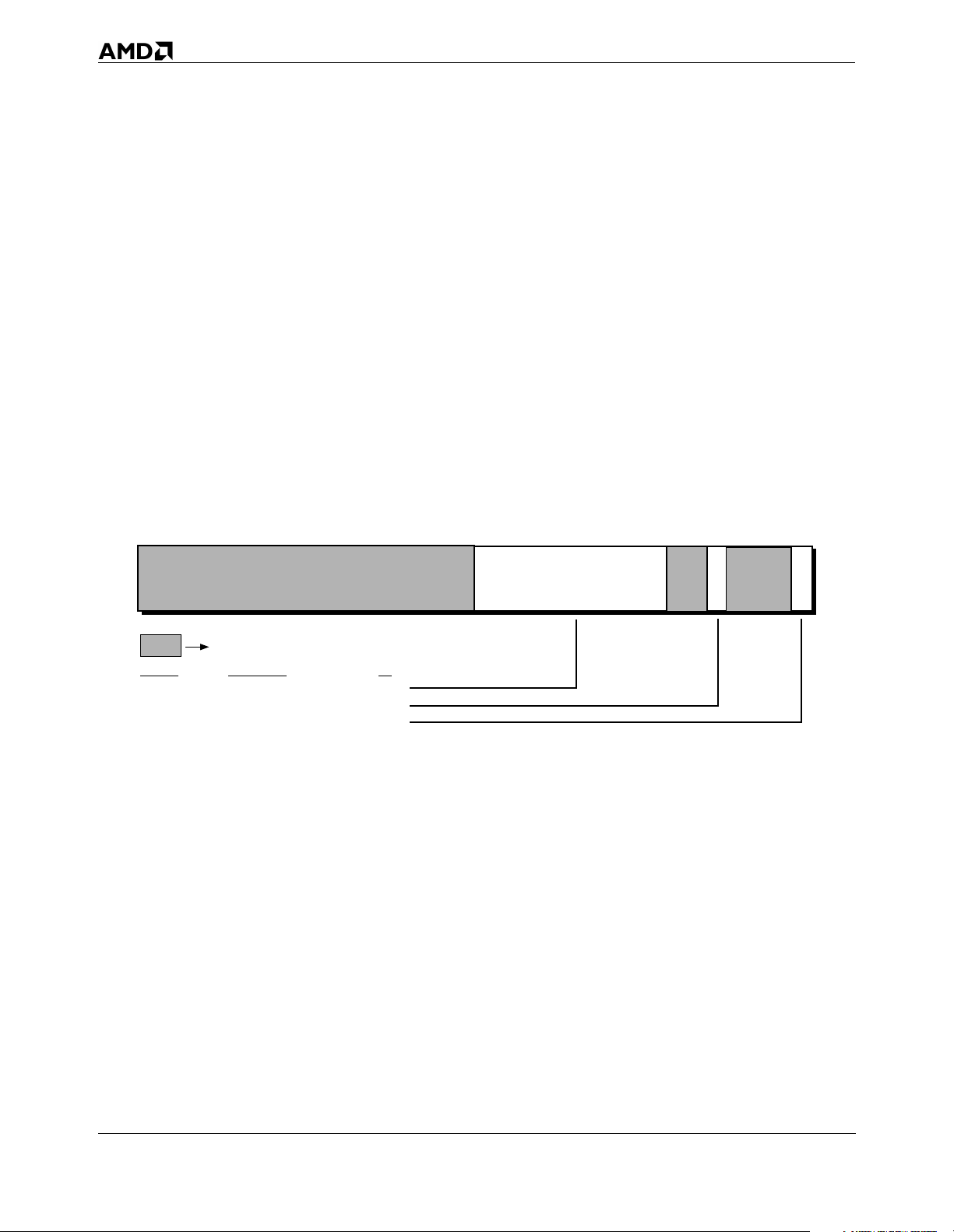
Preliminary Information
Embedded AMD-K6™ Processors BIOS Design Guide 23913A/0—November 2000
Page Flush/Invalidate Register (PFIR)
Models 8/[F:8], 9, and D contain the Page Flush/Invalidate
Register (PFIR) (see Figure 9) that allows cache invalidation
and optional flushing of a specific 4-Kbyte page from the linear
address space.
The total amount of L1 cache in the processor is 64 Kbytes.
Using this register can result in a much lower cycle count for
flushing particular pages versus flushing the entire cache.
When the PFIR is written to (using the WRMSR instruction),
the invalidation and, optionally, the flushing begins.
The PFIR register is MSR C000_0088h.
Note: The invalidate and flush operations affect both the L1 and
L2 caches on models 9 and D.
63
Reserved
Symbol Description Bit
LINPAGE 20-bit Linear Page Address 31-12
PF Page Fault Occurred 8
F/I Flush/Invalidate Command 0
32
LINPAGE
1131 12
987
P
F
10
F
/
I
Figure 9. Page Flush/Invalidate Register (PFIR) (Models 8/[F:8], 9, and D)
LINPAGE Field This 20-bit field must be written with bits 31:12 of the linear
address of the 4-Kbyte page that is to be invalidated and
optionally flushed from the L1 cache.
PF Bit If an attempt to invalidate or flush a page results in a page
fault, the processor sets the PF bit to 1, and the invalidate or
flush operation is not performed (even though invalidate
operations do not normally generate page faults). In this case,
an actual page fault exception is not generated.
If the PF bit equals 0 after an invalidate or flush operation,
then the operation executed successfully. The PF bit must be
read after every write to the PFIR register to determine if the
invalidate or flush operation executed successfully.
36 Model 8/[F:8] Registers

Preliminary Information
23913A/0—November 2000 Embedded AMD-K6™ Processors BIOS Design Guide
F/I Bit This bit is used to control the type of action that occurs to the
specified linear page. If a 0 is written to this bit, the operation
is a flush, in which case all cache lines in the modified state
within the specified page are written back to memory, after
which the entire page is invalidated. If a 1 is written to this bit,
the operation is an invalidation, in which case the entire page is
invalidated without the occurrence of any writebacks.
Model 8/[F:8] Registers 37
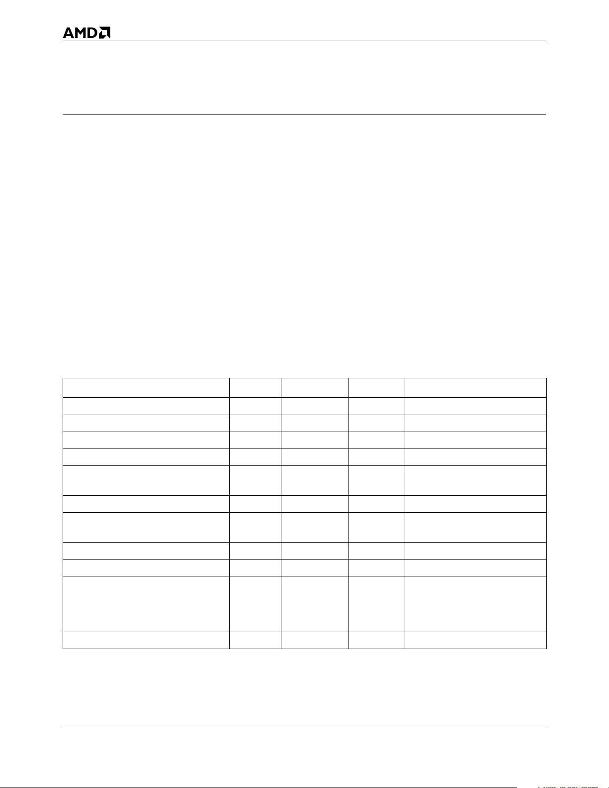
Preliminary Information
Embedded AMD-K6™ Processors BIOS Design Guide 23913A/0—November 2000
Model 9 Registers
The AMD-K6-III processor (Model 9) provides the eleven modelspecific registers listed in Table 19.
The contents of ECX selects the MSR to be addressed by the
RDMSR and WRMSR instruction.
The AMD-K6-III processor contains a split Level-1 (L1)
64-Kbyte writeback cache organized as a separate 32-Kbyte
instruction cache and a 32-Kbyte data cache with two-way set
associativity. The cache line size is 32 bytes, and lines are read
from memory using an efficient pipelined burst read cycle. In
addition, the processor also contains a 256-Kbyte, 4-way set
associative, unified level-2 (L2) cache. Further performance
gains are achieved by the implementation of a write allocation
scheme.
Table 19. Model-Specific Registers Supported by Model 9
Register Name Mnemonic ECX Value Description Comments
Machine-Check Address Register MCAR 00h page 16 Identical on all models
Machine-Check Type Register MCTR 01h page 16 Identical on all models
Test Register 12 TR12 0Eh page 16 Identical on all models
Time Stamp Counter TSC 10h page 16 Identical on all models
Extended Feature Enable Register EFER C000_0080h page 39
Write Handling Control Register WHCR C000_0082h page 27 Identical to Model 8/[F:8]
SYSCALL/SYSRET Target Address Regis-
ter
UC/WC Cacheability Control Register UWCCR C000_0085h page 30 Identical to Model 8/[F:8]
Processor State Observability Register PSOR C000_0087h page 34 Identical to Model 8/[F:8]
Page Flush/Invalidate Register PFIR C000_0088h page 36
Level-2 Cache Array Access Register L2AAR C000_0089h page 40 New for Model 9
STAR C000_0081h page 22 Identical to Model 8/[7:0]
Adds L2 Disable bit (L2D) to
Model 8/[F:8] implementation
Identical to Model 8/[F:8]. The
invalidate and flush operations
affect both the L1 and L2 caches
on the AMD-K6-III processor.
38 Model 9 Registers
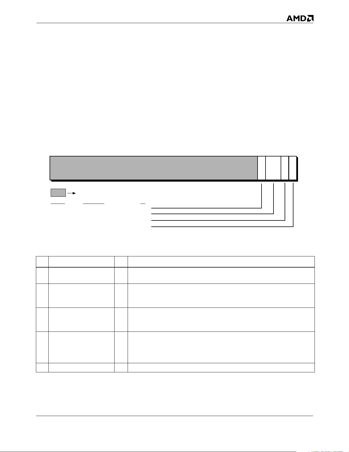
Preliminary Information
23913A/0—November 2000 Embedded AMD-K6™ Processors BIOS Design Guide
Extended Feature Enable Register (EFER)
Figure 10 shows the format of the EFER register for models 9
and D, and Table 20 defines the function of each bit of the
EFER register. The EFER register is MSR C000_0080h.
Note: Bits 3:0 of the EFER register in models 9 and D are identical
to the implementation of these bits in Model 8/[F:8]. For
models 9 and D, the L2 Disable bit (L2D), EFER[4], is
added. The complete new register description is included in
this section.
1063
5
234
Reserved
Symbol Description Bit
L2D L2 Disable 4
EWBEC EWBE Control 3-2
DPE Data Prefetch Enable 1
SCE System Call Extension 0
Figure 10. Extended Feature Enable Register (EFER) (Models 9 and D)
Table 20. Extended Feature Enable Register (EFER) Definition (Models 9 and D)
Bit Description R/W Function
Writing a 1 to any reserved bit causes a general protection fault to occur. All
63–5
Reserved
4
L2 Disable (L2D)
3-2
EWBE Control (EWBEC)
1
Data Prefetch Enable (DPE)
0
System Call Extension (SCE)
R
reserved bits are always read as 0.
If L2D is set to 1, the L2 cache is completely disabled. This bit is provided for
R/W
debug and testing purposes. For normal operation and maximum performance,
this bit must be set to 0 (this is the default setting following reset).
This 2-bit field controls the behavior of the processor with respect to the ordering
R/W
of write cycles and the EWBE# signal. EFER[3] and EFER[2] are Global EWBE#
Disable (GEWBED) and Speculative EWBE# Disable (SEWBED), respectively.
DPE must be set to 1 to enable data prefetching (this is the default setting following reset). If enabled, cache misses initiated by a memory read within a 32-byte
R/W
cache line are conditionally followed by cache-line fetches of the other line in the
64-byte sector.
R/W
SCE must be set to 1 to enable usage of the SYSCALL and SYSRET instructions.
L
2
D
EWBEC
S
D
C
P
E
E
Note: Setting L2D to 1 does not guarantee cache coherency. To
ensure coherency, the processor’s caches must be disabled
(by setting the CD bit of the CR0 register to 1), then flushed
prior to setting L2D to 1.
Model 9 Registers 39
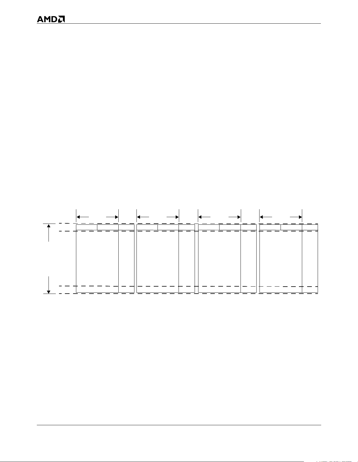
Preliminary Information
Embedded AMD-K6™ Processors BIOS Design Guide 23913A/0—November 2000
Level-2 Cache Array Access Register (L2AAR)
Models 9 and D provide the L2AAR register that allows for
direct access to the L2 cache and L2 tag arrays. The L2 cache in
the AMD-K6-III processor is organized as shown in Figure 11:
■ Four 64-Kbyte ways
■ Each way contains 1024 sets
■ Each set contains four 64-byte sectors (one sector in each
way)
■ Each sector contains two 32-byte cache lines
■ Each cache line contains four 8-byte octets
■ Each octet contains an upper and lower dword (4 bytes)
Each line within a sector contains its own MESI state bits, and
associated with each sector is a tag and least recently used
(LRU) information.
Line1/MESI
64 bytes
Way 1
Line0/MESI
Tag/LRU
1024 sets
Set 0
Set 1023
Line1/MESI
64 bytes
Way 0
Line0/MESI
Tag /L RU
Figure 11. L2 Cache Organization (AMD-K6™-III Processor)
The L2AAR register is MSR C000_0089h.
The operation that is performed on the L2 cache is a function of
the instruction executed—RDMSR or WRMSR—and the
contents of the EDX register. The EDX register specifies the
location of the access, and whether the access is to the L2 cache
data or tags (see Figure 13 on page 41).
Figure 12 on page 41 shows the L2 cache sector and line
organization. If bit 5 (see Figure 13) of the address of a cache
line equals 1, then this cache line is stored in Line 1 of a sector.
Similarly, if bit 5 of the address of a cache line equals 0, then
this cache line is stored in Line 0 of a sector.
Line1/MESI
64 bytes
Line0/MESI
Way 2
Tag/LRU
Line1/MESI
64 bytes
Line0/MESI
Way 3
Tag/LRU
40 Model 9 Registers

Preliminary Information
23913A/0—November 2000 Embedded AMD-K6™ Processors BIOS Design Guide
Upper Dword Lower DwordOctet 0
Octet 1
Octet 2
Octet 3
Line 1
Figure 12. L2 Cache Sector and Line Organization
Bit 20 of EDX (T/D) determines whether the access is to the L2
cache data or tag. Table 21 on page 42 describes the operation
that is performed based on the instruction and the T/D bit.
Upper Dword Lower Dword
Line 0
Sector
Symbol Description Bit
T/D Selects Tag (1) or Data (0) access 20
Way Selects desired cache way 17-16
2131 20 19 17 16 515
Reserved
Symbol Description Bit
Set Selects the desired cache set 15-6
Line Selects Line1 (1) or Line0 (0) 5
Octet Selects one of four octets 4-3
Dword Selects upper (1) or lower (0) dword 2
18
T
/
D
Way
Set
Figure 13. L2 Tag or Data Location (AMD-K6™-III Processor)—EDX
6
L
i
n
e
4321
D
w
Octet
o
r
d
0
Model 9 Registers 41

Preliminary Information
Embedded AMD-K6™ Processors BIOS Design Guide 23913A/0—November 2000
Table 21. Tag versus Data Selector
Instruction
RDMSR 0
RDMSR 1
WRMSR 0
WRMSR 1
T/D
(EDX[20])
Operation
Read dword from L2 data array into EAX. Dword location
is specified by EDX.
Read tag, line state and LRU information from L2 tag array
into EAX. Location of tag is specified by EDX.
Write dword to the L2 data array using data in EAX. Dword
location is specified by EDX.
Write tag, line state and LRU information into L2 tag array
from EAX. Location of tag is specified by EDX.
When the L2AAR is read or written, EDX is left unchanged.
This facilitates multiple accesses when testing the entire
cache/tag array.
If the L2 cache data is read (as opposed to reading the tag
information), the result (dword) is placed in EAX in the format
as illustrated in Figure 14. Similarly, if the L2 cache data is
written, the write data is taken from EAX.
Figure 14. L2 Data—EAX
031
Data
If the L2 tag is read (as opposed to reading the cache data), the
result is placed in EAX in the format as illustrated in Figure 15
on page 43. Similarly, if the L2 tag is written, the write data is
taken from EAX.
When accessing the L2 tag, the Line, Octet, and Dword fields of
the EDX register are ignored.
42 Model 9 Registers
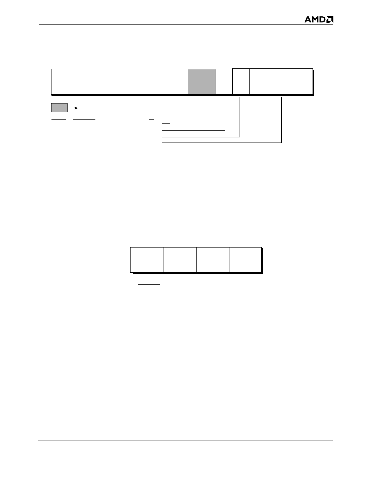
Preliminary Information
23913A/0—November 2000 Embedded AMD-K6™ Processors BIOS Design Guide
1531 14 12 10 9 78
Tag
Reserved
Symbol Description Bit
Tag Tag data read or written 31-15
Line1ST Line 1 state (M=11, E=10, S=01, I=00) 11-10
Line0ST Line 0 state (M=11, E=10, S=01, I=00) 9-8
LRU Two bits of LRU for each way 7-0
Figure 15. L2 Tag Information (AMD-K6™-III Processor)—EAX
LRU (Least Recently Used) Field
For the 4-way set associative L2 cache, each way has a 2-bit LRU
field for each sector. Values for the LRU field are 00b, 01b, 10b,
and 11b, where 00b indicates that the sector is “most recently
used,” and 11b indicates that the sector is “least recently used”
(see Figure 16). EAX[7:6] indicate LRU information for Way 0,
EAX[5:4] for Way 1, EAX[3:2] for Way 2, and EAX[1:0] for
Way 3.
11
Line0STLine1ST
LRU
0
C
M
D
Writing to L2 Tag of
AMD-K6™-III
Processor
765432
Way 2
LRU Values
00b Most Recently Used
01b Used More Recently Than 10b, But Less Recently Than 00b
10b Used More Recently Than 11b, But Less Recently Than 01b
11b Least Recently Used
1
0
Way 3Way 0 Way 1
Figure 16. LRU Byte
When writing to the L2 tag of the AMD-K6-III processor, special
consideration must be given to the least significant bit of the
Tag field of the EAX register— EAX[15]. The length of the L2
tag required to support the 256-Kbyte L2 cache on the
AMD-K6-III processor is 16 bits, which corresponds to bits 31:16
of the EAX register. However, the AMD-K6-III processor
provides a total of 17 bits for storing the L2 tag—that is, 16 bits
for the tag (EAX[31:16]), plus an additional bit for internal
purposes (EAX[15]). During normal operation, the AMD-K6-III
processor ensures that this additional bit (bit 15) always
corresponds to the set in which the tag resides. Note that bits
Model 9 Registers 43

Preliminary Information
Embedded AMD-K6™ Processors BIOS Design Guide 23913A/0—November 2000
15:6 of the address determine the set, in which case bit 15 equal
to 0 addresses sets 0 through 511, and bit 15 equal to 1
addresses sets 512 through 1023.
In order to set the full 17-bit L2 tag properly when using the
L2AAR register, EAX[15] must likewise correspond to the set in
which the tag is being written—that is, EAX[15] must be equal
to EDX[15] (refer to Figure 13 on page 41 and Figure 15 on
page 43).
It is important to note that this special consideration is only
required if the AMD-K6-III processor will subsequently be
expected to properly execute instructions or access data from
the L2 cache following the setup of the L2 cache by means of
the L2AAR register. If the intent of using the L2AAR register is
solely to test or debug the L2 cache without the subsequent
intent of executing instructions or accessing data from the L2
cache, then this consideration is not required.
44 Model 9 Registers

Preliminary Information
23913A/0—November 2000 Embedded AMD-K6™ Processors BIOS Design Guide
Model D Registers
The AMD-K6-2E+ and AMD-K6-IIIE+ processors (Model D)
provide the twelve model-specific registers listed in Table 22.
The contents of ECX selects the MSR to be addressed by the
RDMSR and WRMSR instruction.
The AMD-K6-2E+ and AMD-K6-IIIE+ processors contain a split
Level-1 (L1) 64-Kbyte writeback cache organized as a separate
32-Kbyte instruction cache and a 32-Kbyte data cache with
two-way set associativity. The cache line size is 32 bytes, and
lines are read from memory using an efficient pipelined burst
read cycle. In addition, these processors also contain a 128Kbyte (AMD-K6-2E+ processor) or a 256-Kbyte (AMD-K6-IIIE+
processor), 4-way set associative, unified Level-2 (L2) cache.
Further performance gains are achieved by the implementation
of a write allocation scheme.
Table 22. Model-Specific Registers Supported by Model D
Register Name Mnemonic ECX Value Description Comments
Machine-Check Address Register MCAR 00h page 16 Identical on all models
Machine-Check Type Register MCTR 01h page 16 Identical on all models
Test Register 12 TR12 0Eh page 16 Identical on all models
Time Stamp Counter TSC 10h page 16 Identical on all models
Extended Feature Enable Register EFER C000_0080h page 39
Write Handling Control Register WHCR C000_0082h page 27 Identical to Model 8/[F:8]
SYSCALL/SYSRET Target Address Register STAR C000_0081h page 22 Identical to Model 8/[7:0]
UC/WC Cacheability Control Register UWCCR C000_0085h page 30 Identical to Model 8/[F:8]
Processor State Observability Register PSOR C000_0087h
Page Flush/Invalidate Register PFIR C000_0088h page 36 Identical to Model 8/[F:8]
Level-2 Cache Array Access Register L2AAR C000_0089h page 48
2
Enhanced Power Management Register
EPMR C000_0086h page 54
page 34
page 46
Adds L2 Disable bit (L2D) to Model
8/[F:8] implementation
Standard-power implementation is
1
,
identical to Model 8/[F:8]. Low-
2
power implementation adds new
fields and renames BF to EBF.
Identical to Model 9, but note differing L2 cache sizes on Model D.
New for Model D. Supported on
low-power versions only.
Notes:
1. Standard-power versions only.
2. Low-power versions only.
Model D Registers 45

Preliminary Information
Embedded AMD-K6™ Processors BIOS Design Guide 23913A/0—November 2000
Processor State Observability Register (PSOR) (Low-Power Versions)
The low-power versions of the AMD-K6-2E+ and AMD-K6-IIIE+
processors provide the Processor State Observability Register
(PSOR) as defined in Figure 17.
Note: Standard-power versions of Model D support the PSOR as
defined on page 34.
The PSOR register is MSR C000_0087h.
.
Symbol Description Bits
PBF Pin Bus Frequency Divisor 23-21
VID Voltage ID 20-16
63
Reserved
Symbol Description Bits
NOL2 No L2 Functionality 8
STEP Processor Stepping 7-4
EBF Effective Bus Frequency Divisor 2-0
24
23
21 15
PBF[2:0]
VID
1620
789
N
O
STEP
L
2
34
2
EBF[2:0]
0
Figure 17. Processor State Observability Register (PSOR) (Model D Low-Power Versions)
PBF[2:0] Field This read-only field contains the BF divisor values externally
applied to the processor BF[2:0] pins. These input BF values are
sampled by the processor during the falling transition of
RESET.
Note: This BF divisor value may be different than the BF divisor
value supplied to the processor’s internal PLL.
VID Field This read-only field contains the Voltage ID bits driven to the
processor VID[4:0] pins at RESET. These bits are initialized to
01010b and driven on the VID[4:0] pins at RESET.
Note: Low-power AMD-K6-2E+ and AMD-K6-IIIE+ processors
support AMD PowerNow! technology, which enables
dynamic alteration of the processor’s core voltage. See
“Enhanced Power Management Register (EPMR) (LowPower Versions)” on page 54 for information on
programming the VID[4:0] pins.
46 Model D Registers
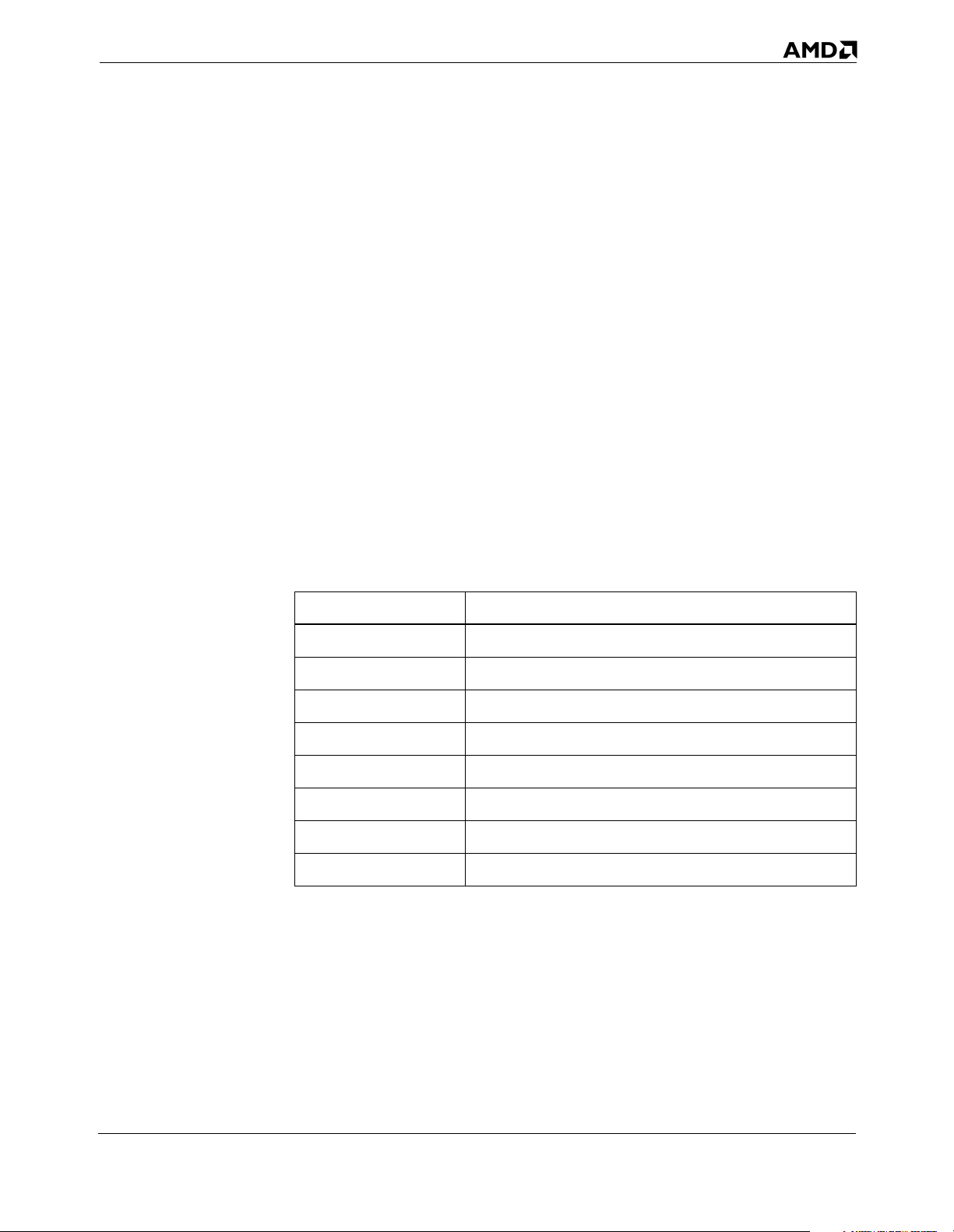
Preliminary Information
23913A/0—November 2000 Embedded AMD-K6™ Processors BIOS Design Guide
NOL2 Bit This read-only bit indicates whether the processor contains an
L2 cache.
Note: This bit is always set to 0 for Model D.
STEP Field This read-only field contains the stepping ID. This is identical to
the value returned by CPUID standard function 1 in EAX[3:0].
EBF[2:0] Field This read-only field contains the effective value of the BF
divisor supplied to the processor’s internal PLL, which allows
the BIOS to determine the frequency of the host bus.
■ The core frequency must first be determined using the Time
Stamp Counter method (See “Time Stamp Counter (TSC)”
on page 16).
■ The core frequency is then divided by the processor-to-bus
clock ratio as determined by the EBF field of the PSOR
register (see Table 23).
■ The result is the frequency of the processor bus.
Table 23. Processor-to-Bus Clock Ratios (Low-Power Model D)
State of EBF[2:0] Processor-to-Bus Clock Ratio
100b 2.0x
101b 3.0x
110b 6.0x
111b 3.5x
000b 4.5x
001b 5.0x
010b 4.0x
011b 5.5x
Notes:
1. The 2.5x ratio that was supported on Models 8 and 9 is not supported on low-power Model D.
Instead, a ratio of 2.0x is selected when EBF[2:0] equals 100b.
1
Model D Registers 47

Preliminary Information
Embedded AMD-K6™ Processors BIOS Design Guide 23913A/0—November 2000
Level-2 Cache Array Access Register (L2AAR)
Model D also provides the L2AAR register that allows for direct
access to the L2 cache and L2 tag arrays.
Note: The L2AAR register is identical to the Model 9
implementation. Some information in this section is
duplicated to account for the different L2 cache sizes in the
AMD-K6-2E+ and AMD-K6-IIIE+ processors.
The L2 cache in the AMD-K6-2E+ and AMD-K6-IIIE+ processors
is organized as shown in Figure 18:
■ Four 32-Kbyte ways (AMD-K6-2E+ processor) or four 64-
Kbyte ways (AMD-K6-IIIE+ processor)
■ Each way contains 512 (AMD-K6-2E+ processor) or 1024
(AMD-K6-IIIE+ processor) sets
512 or 1024 sets
Set 0
Set 1023
Line1/MESI
64 bytes
Way 0
■ Each set contains four 64-byte sectors (one sector in each
way)
■ Each sector contains two 32-byte cache lines
■ Each cache line contains four 8-byte octets
■ Each octet contains an upper and lower dword (4 bytes)
Each line within a sector contains its own MESI state bits, and
associated with each sector is a tag and LRU (Least Recently
Used) information.
Line0/MESI
Tag /L RU
Line1/MESI
64 bytes
Way 1
Line0/MESI
Tag/LRU
Line1/MESI
64 bytes
Line0/MESI
Way 2
Tag/LRU
Line1/MESI
64 bytes
Line0/MESI
Way 3
Tag/LRU
Figure 18. L2 Cache Organization
48 Model D Registers

Preliminary Information
23913A/0—November 2000 Embedded AMD-K6™ Processors BIOS Design Guide
The L2AAR register is MSR C000_0089h.
The operation that is performed on the L2 cache is a function of
the instruction executed—RDMSR or WRMSR—and the
contents of the EDX register. The EDX register specifies the
location of the access, and whether the access is to the L2 cache
data or tags (refer to Figure 20 on page 50 for the AMD-K6-2E+
processor and Figure 21 on page 50 for the AMD-K6-IIIE+
processor).
Figure 19 shows the L2 cache sector and line organization. If bit
5 (refer to Figure 20 for the AMD-K6-2E+ processor and Figure
21 for the AMD-K6-IIIE+ processor) of the address of a cache
line equals 1, then this cache line is stored in Line 1 of a sector.
Similarly, if bit 5 of the address of a cache line equals 0, then
this cache line is stored in Line 0 of a sector.
Upper Dword Lower DwordOctet 0
Octet 1
Octet 2
Octet 3
Line 1
Sector
Upper Dword Lower Dword
Figure 19. L2 Cache Sector and Line Organization (same as Figure 12)
Bit 15 of EDX, which is the most significant bit of the Set field,
is not used for the AMD-K6-2E+ because there are half as many
sets implemented on the AMD-K6-2E+ (512 sets) as the
AMD-K6-IIIE+ processor (1024 sets). Bit 20 of EDX (T/D)
determines whether the access is to the L2 cache data or tag.
Table 24 on page 51 describes the operation that is performed
based on the instruction and the T/D bit.
Line 0
Model D Registers 49

Preliminary Information
Embedded AMD-K6™ Processors BIOS Design Guide 23913A/0—November 2000
Symbol Description Bit
T/D Selects Tag (1) or Data (0) access 20
Way Selects desired cache way 17-16
2131 20 19 17 16 515
Reserved
Symbol Description Bit
Set Selects the desired cache set 14-6
Line Selects Line1 (1) or Line0 (0) 5
Octet Selects one of four octets 4-3
Dword Selects upper (1) or lower (0) dword 2
18
T
/
D
Way
14
Set
Figure 20. L2 Tag or Data Location (AMD-K6™-2E+ Processor)—EDX
Symbol Description Bit
T/D Selects Tag (1) or Data (0) access 20
Way Selects desired cache way 17-16
2131 20 19 17 16 515
18
T
/
D
Way
Set
6
L
i
n
e
6
L
i
n
e
4321
D
w
Octet
o
r
d
4321
D
w
Octet
o
r
d
0
0
Reserved
Symbol Description Bit
Set Selects the desired cache set 15-6
Line Selects Line1 (1) or Line0 (0) 5
Octet Selects one of four octets 4-3
Dword Selects upper (1) or lower (0) dword 2
Figure 21. L2 Tag or Data Location (AMD-K6™-IIIE+ Processor)—EDX
50 Model D Registers

Preliminary Information
23913A/0—November 2000 Embedded AMD-K6™ Processors BIOS Design Guide
Table 24. Tag versus Data Selector (same as Table 21)
Instruction
RDMSR 0
RDMSR 1
WRMSR 0
WRMSR 1
T/D
(EDX[20])
Operation
Read dword from L2 data array into EAX. Dword location
is specified by EDX.
Read tag, line state and LRU information from L2 tag array
into EAX. Location of tag is specified by EDX.
Write dword to the L2 data array using data in EAX. Dword
location is specified by EDX.
Write tag, line state and LRU information into L2 tag array
from EAX. Location of tag is specified by EDX.
When the L2AAR is read or written, EDX is left unchanged.
This facilitates multiple accesses when testing the entire
cache/tag array.
If the L2 cache data is read (as opposed to reading the tag
information), the result (dword) is placed in EAX in the format
as illustrated in Figure 22. Similarly, if the L2 cache data is
written, the write data is taken from EAX.
Figure 22. L2 Data—EAX (same as Figure 14)
If the L2 tag is read (as opposed to reading the cache data), the
result is placed in EAX in the format as illustrated in Figure 23
on page 52 (AMD-K6-2E+ processor) and Figure 24
(AMD-K6-IIIE+ processor). Similarly, if the L2 tag is written,
the write data is taken from EAX.
When accessing the L2 tag, the Line, Octet, and Dword fields of
the EDX register are ignored.
031
Data
Model D Registers 51
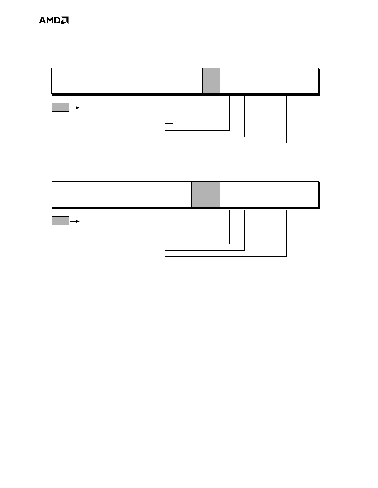
Preliminary Information
Embedded AMD-K6™ Processors BIOS Design Guide 23913A/0—November 2000
31 14 12 10 9 7811
Tag
Reserved
Symbol Description Bit
Tag Tag data read or written 31-14
Line1ST Line 1 state (M=11, E=10, S=01, I=00) 11-10
Line0ST Line 0 state (M=11, E=10, S=01, I=00) 9-8
LRU Two bits of LRU for each way 7-0
13
Figure 23. L2 Tag Information (AMD-K6™-2E+ Processor)—EAX
1531 14 12 10 9 7811
Tag
Reserved
Symbol Description Bit
Tag Tag data read or written 31-15
Line1ST Line 1 state (M=11, E=10, S=01, I=00) 11-10
Line0ST Line 0 state (M=11, E=10, S=01, I=00) 9-8
LRU Two bits of LRU for each way 7-0
0
Line0STLine1ST
Line0STLine1ST
LRU
LRU
C
M
D
0
C
M
D
Figure 24. L2 Tag Information (AMD-K6™-IIIE+ Processor)—EAX
LRU (Least Recently Used) Field
For the 4-way set associative L2 cache, each way has a 2-bit LRU
field for each sector. Values for the LRU field are 00b, 01b, 10b,
and 11b, where 00b indicates that the sector is “most recently
used,” and 11b indicates that the sector is “least recently used”
(see Figure 25 on page 53). EAX[7:6] indicate the LRU
information for Way 0, EAX[5:4] for Way 1, EAX[3:2] for Way 2,
and EAX[1:0] for Way 3.
52 Model D Registers

Preliminary Information
23913A/0—November 2000 Embedded AMD-K6™ Processors BIOS Design Guide
Writing to L2 Tag of
AMD-K6-IIIE+
Processor
765432
Way 2
LRU Values
00b Most Recently Used
01b Used More Recently Than 10b, But Less Recently Than 00b
10b Used More Recently Than 11b, But Less Recently Than 01b
11b Least Recently Used
1
0
Way 3Way 0 Way 1
Figure 25. LRU Byte (same as Figure 16)
When writing to the L2 tag of the AMD-K6-IIIE+ processor,
special consideration must be given to the least significant bit
of the Tag field of the EAX register— EAX[15]. The length of
the L2 tag required to support the 256-Kbyte L2 cache on the
AMD-K6-III and AMD-K6-IIIE+ is 16 bits, which corresponds to
bits 31:16 of the EAX register. However, the AMD-K6-IIIE+
processor provides a total of 17 bits for storing the L2 tag—that
is, 16 bits for the tag (EAX[31:16]), plus an additional bit for
internal purposes (EAX[15]). During normal operation, the
AMD-K6-III and AMD-K6-IIIE+ ensure that this additional bit
(bit 15) always corresponds to the set in which the tag resides.
Note that bits 15:6 of the address determine the set, in which
case bit 15 equal to 0 addresses sets 0 through 511, and bit 15
equal to 1 addresses sets 512 through 1023.
In order to set the full 17-bit L2 tag properly when using the
L2AAR register, EAX[15] must likewise correspond to the set in
which the tag is being written—that is, EAX[15] must be equal
to EDX[15] (refer to Figure 21 on page 50 and Figure 24 on
page 52).
It is important to note that this special consideration is only
required if the AMD-K6-IIIE+ processor will subsequently be
expected to properly execute instructions or access data from
the L2 cache following the setup of the L2 cache by means of
the L2AAR register. If the intent of using the L2AAR register is
solely to test or debug the L2 cache without the subsequent
intent of executing instructions or accessing data from the L2
cache, then this consideration is not required.
Note: This special consideration when writing to the L2 tag is not
applicable to the AMD-K6-2E+ processor.
Model D Registers 53
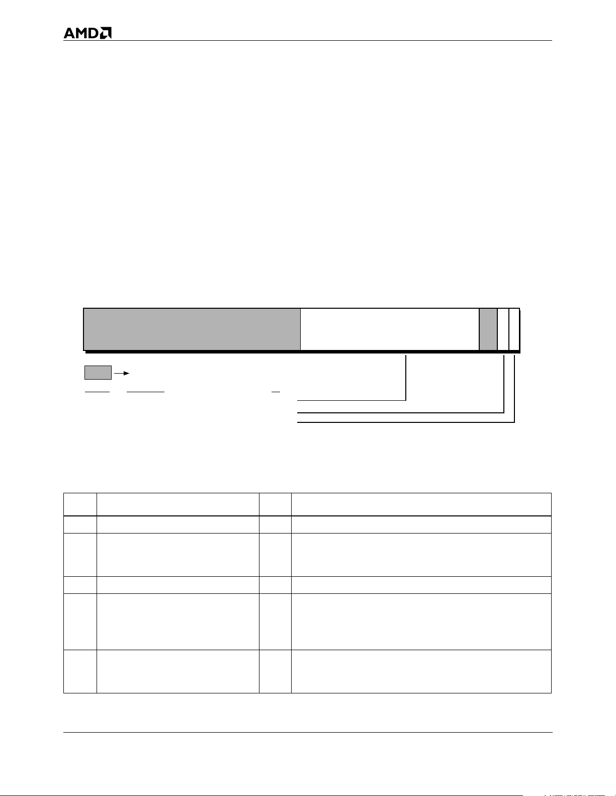
Preliminary Information
Embedded AMD-K6™ Processors BIOS Design Guide 23913A/0—November 2000
Enhanced Power Management Register (EPMR) (Low-Power Versions)
To support AMD PowerNow! technology, the low-power versions
of the AMD-K6-2E+ and AMD-K6-IIIE+ processors Model D are
designed with enhanced power management (EPM) features:
dynamic bus divisor control, and dynamic voltage ID control.
The EPMR register (see Figure 26) defines the base address for
a 16-byte block of I/O address space. Enabling the EPMR allows
software to access the EPM 16-byte I/O block, which contains
bits for enabling, controlling, and monitoring the EPM features.
Table 25 defines the functions of each bit in the EPMR register.
The EPMR register is MSR C000_0086h.
31
1663 15
IOBASE
Reserved
Symbol Description Bit
IOBASE I/O Base Address 15-4
GSBC Generate Special Bus Cycle 1
EN Enable AMD PowerNow! Technology
Management 0
4
Figure 26. Enhanced Power Management Register (EPMR) (Low-Power Model D)
Table 25. Enhanced Power Management Register (EPMR) Definition (Low-Power Model D)
Bit Description R/W
63–16
Reserved
15-4
I/O BASE Address (IOBASE)
3-2
Reserved
Function
R
All reserved bits are always read as 0.
IOBASE defines a base address for a 16-byte block of I/O
R/W
address space accessible for enabling, controlling, and monitoring the EPM features.
R
All reserved bits are always read as 0.
1
0
2
G
C
E
S
M
N
B
D
C
This bit controls whether a special bus cycle is generated upon
1
Generate Special Bus Cycle (GSBC)
dword accesses within the EPM 16-byte block. If set to 1, an
R/W
EPM special bus cycle is generated, where BE[7:0]# = BFh and
A[4:3] = 00b.
Enable AMD PowerNow! Technology
0
Management (EN)
Notes:
1. All bits default to 0 when RESET is asserted.
This bit controls access to the mapped I/O address space for
R/W
the EPM features. Clearing this bit does not affect the state of
bits defined in the EPM 16-byte I/O block.
54 Model D Registers
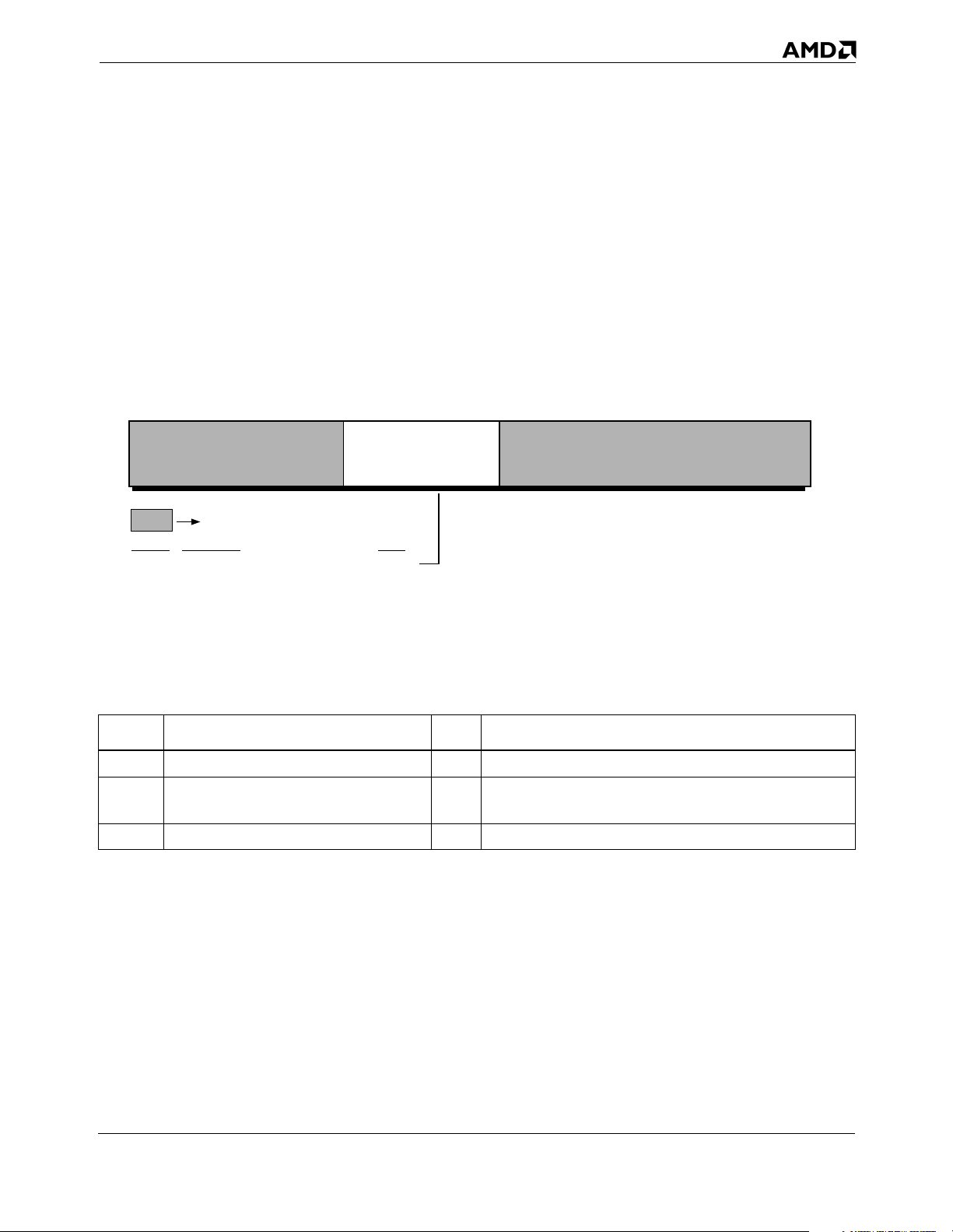
Preliminary Information
23913A/0—November 2000 Embedded AMD-K6™ Processors BIOS Design Guide
EPM 16-Byte I/O Block (Low-Power Versions Only)
The EPM 16-byte I/O block contains one 4-byte field—Bus
Divisor and Voltage ID Control (BVC)—for enabling,
controlling, and monitoring the EPM features (see Figure 27).
All accesses to the EPM 16-byte I/O block must be aligned
dword accesses. Except for the EPM special bus cycle, valid
accesses to the EPM 16-byte block do not generate I/O bus
cycles, while non-aligned and non-dword accesses are passed to
the I/O bus.
15 11
Reserved
Symbol Description Bytes
BVC Bus Divisor and Voltage ID Control 11-8
12
BVC
87
Figure 27. EPM 16-Byte I/O Block (Low-Power Model D)
Table 26 defines the function of the byte-field within the EPM
16-byte I/O block mapped by the EPMR.
Table 26. EPM 16-Byte I/O Block Definition (Low-Power Model D)
Byte Description R/W
15-12
11-8
7-0
Reserved
Bus Divisor and Voltage ID Control (BVC)
Reserved
R
R/W
R
Function
All reserved bits are always read as 0.
The bit fields within the BVC bytes allow software to
change the processor bus divisor and core voltage.
All reserved bits are always read as 0.
1
0
Notes:
1. All bits default to 0 when RESET is asserted.
BVC Field Figure 28 on page 56 shows the format and Table 27 defines the
function of each bit of the BVC field located within the 16-byte
I/O block.
Note: The EPM Stop Grant state is a low-power, clock-control state
entered by writing a non-zero value to the SGTC field for
altering the core voltage and frequency settings. Systeminitiated inquire (snoop) cycles are not supported and must
be prevented during EPM Stop Grant clock control state.
Model D Registers 55
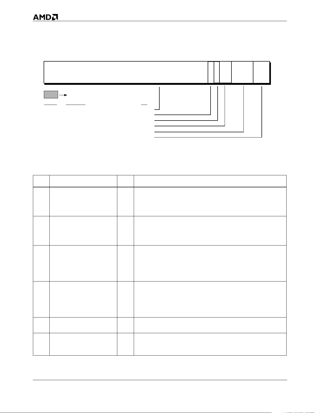
Preliminary Information
Embedded AMD-K6™ Processors BIOS Design Guide 23913A/0—November 2000
31
SGTC
Reserved
Symbol Description Bits
SGTC Stop Grant Time-out Counter 31-12
BVCM Bus Divisor and VID Change Mode 11
VIDC Voltage ID Control 10
BDC Bus Divisor Control 9-8
IBF[2:0] Internal BF Divisor 7-5
VIDO Voltage ID Output 4-0
12
V
B
I
V
D
C
C
M
BDC
IBF[2:0]
9875
11 10
Figure 28. Bus Divisor and Voltage ID Control (BVC) Field (Low-Power Model D)
Table 27. Bus Divisor and Voltage ID Control (BVC) Definition (Low-Power Model D)
Bit Description R/W
Stop Grant Time-out Counter
31-12
(SGTC)
Function
Writing a non-zero value to this field causes the processor to enter the
EPM Stop Grant state internally. This 20-bit value is multiplied by 4096
W
to determines the duration of the EPM Stop Grant state, measured in
processor bus clocks.
1
4
0
VIDO
This bit controls the mode in which the bus-divisor and the voltage con-
Bus Divisor and VID Change
11
Mode (BVCM)
trol bits are allowed to change. If BVCM=0, the Bus Divisor and Voltage
R/W
ID changes take effect only upon entering the EPM Stop Grant state as
a result of the SGTC field being programmed. BVCM=1 is reserved.
This bit controls the mode of Voltage ID control. If VIDC=0, the processor VID[4:0] pins are unchanged upon entering the EPM Stop Grant
10
Voltage ID Control (VIDC)
R/W
state. If VIDC=1, the processor VID[4:0] pins are programmed to the
VIDO value upon entering the EPM Stop Grant state. BIOS should ini-
tialize this bit to 1 during the POST routine.
This 2-bit field controls the mode of bus divisor control. If
BDC[1:0]=00b, the BF[2:0] pins are sampled at the falling edge of
9-8
Bus Divisor Control (BDC)
R/W
RESET. If BDC[1:0]=1xb, the IBF[2:0] field is sampled upon entering the
EPM Stop Grant state. BDC[1:0]=01b is reserved. BIOS should initialize
these bits to 10b during the POST routine.
7-5
Internal BF Divisor (IBF)
If BDC[1:0]=1xb, the processor EBF[2:0] field of the PSOR is pro-
R/W
grammed to the IBF[2:0] value upon entering the EPM Stop Grant state.
This 5-bit value is driven out on the processor VID[4:0] pins upon enter-
4-0 Voltage ID Output (VIDO) R/W
ing the EPM Stop Grant state if the VIDC bit=1. These bits are initialized
to 01010b and driven on the processor VID[4:0] pins at RESET.
Notes:
1. All bits default to 0 when RESET is asserted, except the VIDO bits which default to 01010b.
56 Model D Registers

Preliminary Information
23913A/0—November 2000 Embedded AMD-K6™ Processors BIOS Design Guide
Embedded AMD Processor Recognition
The CPUID instruction provides a simple way for hardware and
software to identify the type of processor and its feature set.
After detecting the processor and its capabilities, software can
be accurately tuned to the system for optimal performance and
benefit to users.
■ For example, game software can test the performance level
available from a particular processor by detecting the type
or speed of the processor. If the features warrant executing
additional capabilities or advanced algorithms, these can be
enabled with software.
■ Another example involves testing for the presence of
3DNow! or MMX instructions on the processor. If the
software finds these features present when it checks the
feature bits, it can utilize these more powerful extensions
for dramatically better performance on new multimedia
software.
See http://www.amd.com/products/cpg/bin for example software
and source code to detect processor information.
CPUID Instruction Overview
Software operating at any privilege level can execute the
CPUID instruction to identify the processor and its feature set.
In addition, the CPUID instruction implements multiple
functions, each providing different information about the
processor, including the vendor, model number, revision
(stepping), features, cache organization, and processor name.
The multiple-function approach allows the CPUID instruction
to return a complete picture about the type of processor and its
capabilities—more detailed information than could be
returned by a single function. The CPUID instruction provides
the flexibility of making only one call to obtain the specific data
requested.
The functions are divided into two types: standard functions
and extended functions.
Embedded AMD Processor Recognition 57

Preliminary Information
Embedded AMD-K6™ Processors BIOS Design Guide 23913A/0—November 2000
■ Standard functions provide a simple method for software to
access information common to all x86 processors.
■ Extended functions provide information on extensions
specific to a vendor’s processor (for example, AMD’s
processors).
The flexibility of the CPUID instruction allows for the addition
of new CPUID functions in future generations of processors.
“Appendix A” on page 71 contains a detailed description of the
CPUID instruction.
Testing for the CPUID Instruction
Beginning with the AMD-K6E processor Model 7, all AMD
processors support the CPUID instruction. However, it is still
recommended that software verify that the CPUID instruction
is supported. To use the CPUID instruction, software must first
determine if the processor supports the CPUID instruction.
CPUID support is determined in one of the following ways:
Illegal Instruction Exception Method
EFLAGS ID-Bit
Method
■ Execute the CPUID instruction and check whether an
illegal instruction exception occurs. If an exception occurs,
the processor does not have CPUID support.
■ Check if the ID bit (bit 21) of the EFLAGS register is
writable. If the bit is writable (that is, it can be modified),
the CPUID instruction is supported.
The operating system (OS) environment determines which
approach is more appropriate. These techniques are described
in the following sections.
This technique requires a way for a user program to detect and
handle illegal instruction exceptions. Where such capabilities
are present, this method represents a reliable way of detecting
support for the CPUID instruction. The CPUID sample code
described on page 67 uses this approach.
This technique retrieves the contents of EFLAGS using the
PUSHFD instruction, toggles the ID bit, and uses the POPFD
instruction to write the modified value of the ID bit into the
EFLAGS register. It then retrieves the contents of EFLAGS
using a second PUSHFD instruction and checks whether the
value of the ID bit differs from the original value.
58 Embedded AMD Processor Recognition

Preliminary Information
23913A/0—November 2000 Embedded AMD-K6™ Processors BIOS Design Guide
If the value has changed, the CPUID instruction is available for
identifying the processor and its features. The following code
sample demonstrates the way a program uses the PUSHFD and
POPFD instructions to test the ID bit.
pushfd ; Save EFLAGS to stack
pop eax ; Store EFLAGS in EAX
mov ebx, eax ; Save in EBX for testing later
xor eax, 00200000h ; Switch bit 21
push eax ; Copy changed value to stack
popfd ; Save changed EAX to EFLAGS
pushfd ; Push EFLAGS to top of stack
pop eax ; Store EFLAGS in EAX
cmp eax, ebx ; See if bit 21 has changed
jz NO_CPUID ; If no change, no CPUID
A potential problem with this approach is that an interrupt or a
trap (such as a debug trap) can occur between the POPFD and
the following PUSHFD, and that the interrupt or trap handler
code destroys the value of the ID bit. Where possible, the above
code should be preceded by a CLI instruction and followed by
an STI instruction, which ensures that no interrupts occur
between the POPFD and the PUSHFD. However, traps can still
occur, even if the code is preceded by a CLI instruction and
followed by an STI instruction.
Using CPUID Functions
When software uses the CPUID instruction to identify a
processor, it is important that it uses the instruction
appropriately. The instruction has been defined to make it easy
to identify the type and features of x86 processors
manufactured by many different vendors.
The standard functions (EAX=0 and EAX=1) are the same for
all processors. Having standard functions simplifies software’s
task of testing for and implementing features common to x86
processors. Software can test for these features and, as new x86
processors are released, benefit from these capabilities
immediately.
Extended functions are specific to a vendor’s processor. These
functions provide additional information about AMD
processors that software can use to identify enhanced features
and functions. To test for extended functions, software checks
Embedded AMD Processor Recognition 59
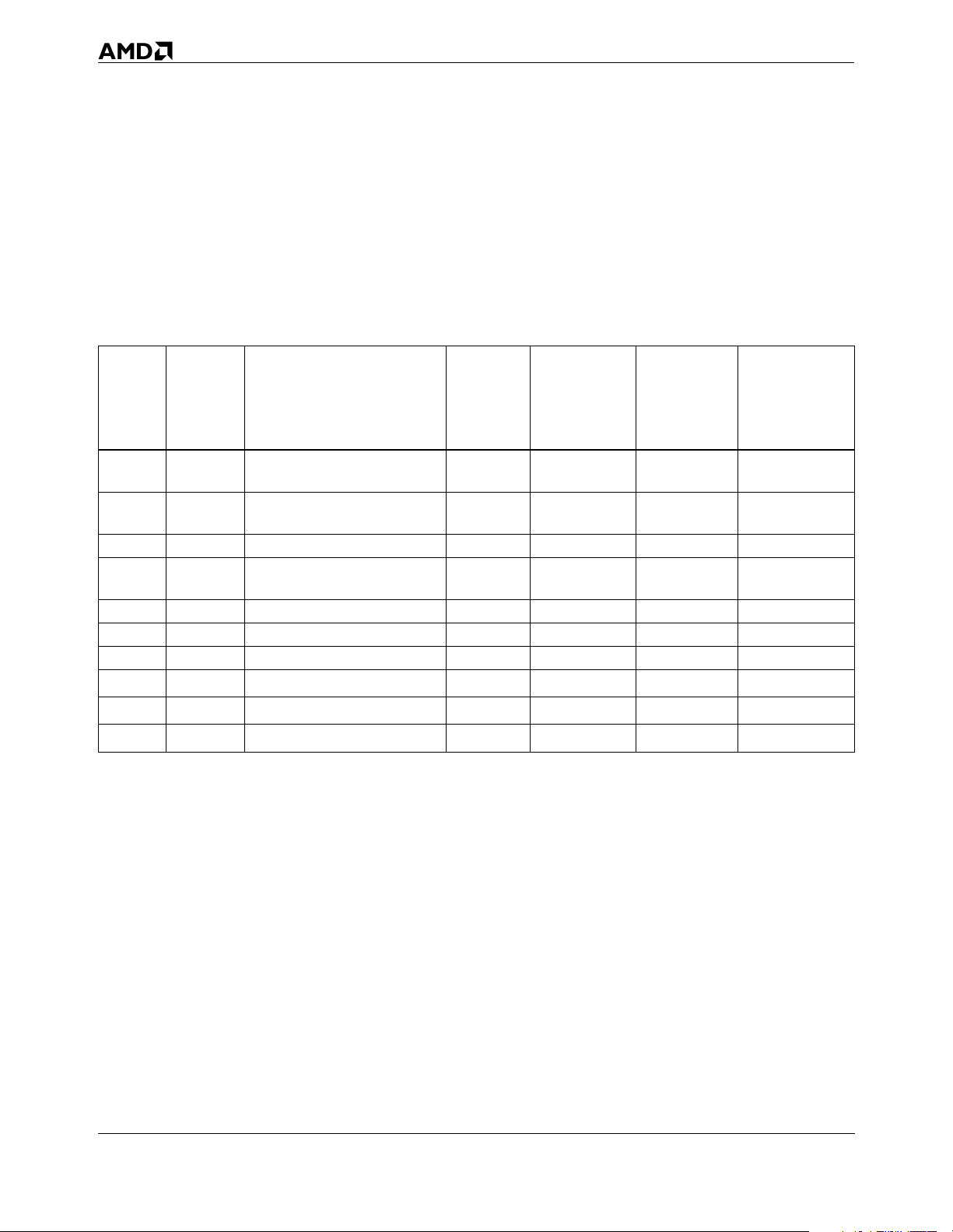
Preliminary Information
Embedded AMD-K6™ Processors BIOS Design Guide 23913A/0—November 2000
for a value of at least 8000_0001h in the EAX register returned
by function 8000_0000h.
Within AMD’s family of processors, different members can
execute a different number of functions. Table 28 summarizes
the CPUID functions currently implemented on AMD
processors.
76
Table 28. CPUID Functions1 in AMD-K6™ Processors2
AMD-K6™-2
and
AMD-K6™E
Standard
Function
0 —
1—
— 8000_0000h Largest Extended Function Value X X X X
— 8000_0001h
— 8000_0002h Processor Name X X X X
— 8000_0003h Processor Name X X X X
— 8000_0004h Processor Name X X X X
— 8000_0005h
— 8000_0006h
— 8000_0007h AMD PowerNow! Technology — — —
Notes:
1. “Appendix A” on page 71 contains detailed descriptions of the functions.
2. Future versions of these processors may implement additional functions.
3. TLB = translation lookaside buffer
4. Low-power versions only
Extended
Function Description
Vendor String and Largest
Standard Function Value
Processor Signature and Standard
Feature Bits
Extended Processor Signature and
Extended Feature Bits
3
Cache Information
L1 TLB
3
Cache Information
L2 TLB
Processor
(Model 7)
XX X X
XX X X
XX X X
XX X X
—— X X
AMD-K6™-2E
Processors
(Model 8)
AMD-K6™-III
Processor
(Model 9)
AMD-K6™-2E+
and
AMD-K6™-IIIE+
Processors
(Model D)
4
X
Identifying the Processor’s Vendor
Software must execute the standard function EAX=0. The
CPUID instruction returns a 12-character string that identifies
the processor’s vendor. The instruction also returns the largest
standard function input value defined for the CPUID
instruction on the processor.
For AMD processors, function 0 returns a vendor string of
“AuthenticAMD”. This string informs the software to follow
60 Embedded AMD Processor Recognition

Preliminary Information
23913A/0—November 2000 Embedded AMD-K6™ Processors BIOS Design Guide
AMD’s definition for subsequent CPUID functions and the
registers returned for those functions.
Once the software identifies the processor’s vendor, it knows
the definition for all the functions supplied by the CPUID
instruction. By using these functions, the software obtains the
processor information needed to properly tune its functionality
to the capabilities of the processor.
Testing For Extended Functions
Software must test for extended functions with function
8000_0000h. The EAX register returns the largest extended
function input value defined for the CPUID instruction on the
processor. If this value is at least 8000_0001h, extended
functions are supported.
With one exception, the AMD extended feature flags include all
the information provided in the standard feature flags as well
as indicators for the additional AMD processor-specific feature
enhancements. The duplication of standard feature bits within
the extended feature bits can minimize the number of function
calls required by software. The exception is bit 11, which
indicates that the SYSENTER and SYSEXIT instructions are
supported in the standard features and that the SYSCALL and
SYSRET instructions are supported in the extended features.
Determining the Processor Signature
Standard function 1 (EAX=1) of the CPUID instruction returns
the standard processor signature and feature bits. The standard
processor signature is returned in the EAX register and
provides information regarding the specific revision (stepping)
and model of the processor and the instruction family level
supported by the processor. The revision level can be used to
determine if the processor supports specific features. However,
it is not recommended that the revision level be used in this
manner unless this information is not available through the
standard or extended feature bits.
Embedded AMD Processor Recognition 61
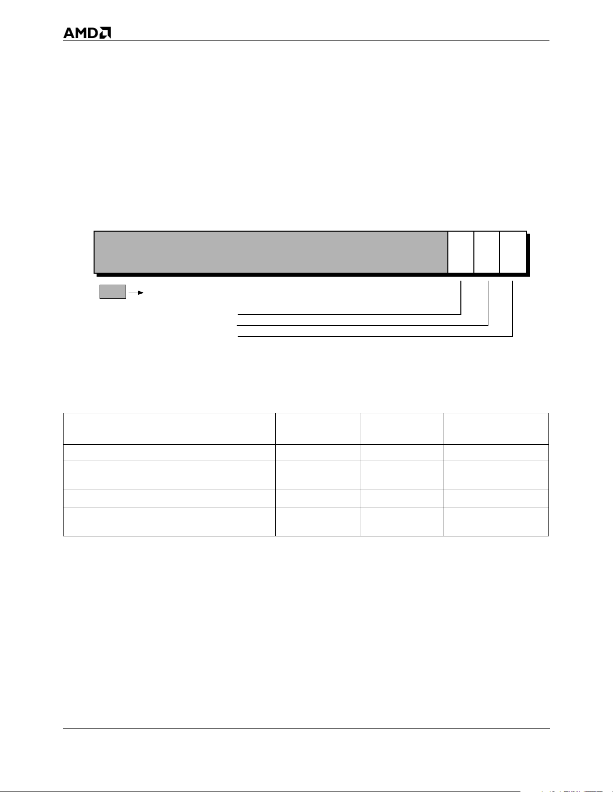
Preliminary Information
Embedded AMD-K6™ Processors BIOS Design Guide 23913A/0—November 2000
All AMD-K6 processor models belong to instruction family 5 (as
returned in EAX by function 1). All AMD Athlon™ processor
models belong to instruction family 6 (as returned in EAX by
function 1).
Figure 29 shows the contents of the EAX register obtained by
function 1. Table 29 summarizes the specific processor
signature values returned for AMD processors.
Reserved
Instruction Family 11–8
Model 7–4
Stepping 3–0
Figure 29. Contents of EAX Register Returned by Function 1
Table 29. Processor Signatures for AMD-K6™ Processors
Processor
AMD-K6E Processor (Model 7)
AMD-K6-2 Processor (Model 8)
AMD-K6-2E Processor (Model 8)
AMD-K6-III Processor (Model 9)
AMD-K6-2E+ Processor (Model D)
AMD-K6-IIIE+ Processor (Model D)
Instruction
Family
0101b (5h) 0111b (7h) xxxx
0101b (5h) 1000b (8h)
0101b (5h) 1001b (9h)
0101b (5h) 1101b (Dh)
Model
12 11 7 3 031
48
Stepping ID
xxxx
xxxx
xxxx
1
Notes:
1. Contact your AMD representative for the latest stepping information. Refer to Table 1 on page 2 for the range of allowable stepping IDs
associated with each model number.
62 Embedded AMD Processor Recognition

Preliminary Information
23913A/0—November 2000 Embedded AMD-K6™ Processors BIOS Design Guide
Identifying Supported Features
The feature bits are returned in the EDX register for two
CPUID functions—standard function 1 and extended function
8000_0001h. Each bit corresponds to a specific feature and
indicates if that feature is present on the processor. Table 30
summarizes the standard and extended feature bits.
Table 30. Standard and Extended Feature Bits
1
Feature Description
Bit
Standard
2
Extended
2
0 Floating-Point Unit A floating-point unit is available. 1 1
1 Virtual Mode Extensions Virtual mode extensions are available. 1 1
2 Debugging Extensions I/O breakpoint debug extensions are supported. 1 1
3 PSE (Page Size Extensions) 4-Mbyte pages are supported. 1 1
Time Stamp Counter
4
(with RDTSC and CR4 disable bit)
K86™ Family of Processors’
5
Model-Specific Registers (with
RDMSR and WRMSR)
6 PAE (Page Address Extensions)
A time stamp counter is available in the processor,
and the RDTSC instruction is supported.
The K86 model-specific registers are available in the
processor, and the RDMSR and WRMSR instructions
are supported.
Page address extensions are supported using an
8-byte directory entry.
11
11
11
7 MCE (Machine Check Exception) The machine check exception is supported. 1 1
8 CMPXCHG8B Instruction The CMPXCHG8B instruction is supported. 1 1
9 APIC A local APIC unit is available. 1 1
10 Reserved on all AMD processors 00
SYSENTER/SYSEXIT Instructions
11
SYSCALL and SYSRET Instructions
MTRR (Memory Type Range
12
Registers)
The SYSENTER and SYSEXIT instructions are
supported.
The SYSCALL and SYSRET instructions and
associated extensions are supported.
10
01
Memory type range registers are available. 1 1
13 Global Paging Extension Global paging extensions are available. 1 1
14 MCA (Machine Check Architecture) Machine check architecture is supported 1 1
15 Conditional Move Instructions
The conditional move instructions CMOV, FCMOV,
and FCOMI are supported.
11
16 PAT (Page Attribute Table) The Page attribute tables are supported. 1 1
17 PSE-36 (Page Size Extension)
Page size extensions for 36-bit addresses are
supported using a 4-byte directory entry.
11
18–21 Reserved on all AMD processors 00
AMD Multimedia Instruction
22
Extensions
AMD additions to the original MMX™ instruction set
are supported.
3
01
Embedded AMD Processor Recognition 63

Preliminary Information
Embedded AMD-K6™ Processors BIOS Design Guide 23913A/0—November 2000
Table 30. Standard and Extended Feature Bits (continued)
1
Feature Description
Bit
23 MMX™ Instructions The MMX instruction set is supported. 1 1
24 FXSAVE/FXRSTOR Fast floating-point save and restore is supported. 1 1
25 Streaming SIMD extensions (SSE)
26 Reserved on all AMD processors 00
AMD 3DNow!™ Instruction
30
Extensions
31 AMD 3DNow! Instructions 3DNow! instructions are supported. 0 1
Notes:
1. “Appendix A” on page 71 contains details on bit values.
2. Bit definitions: 0 = No Support, 1 = Support
3. For more information on these instructions, see the AMD Extensions to the 3DNow!™ and MMX™ Instructions Sets Manual, order#
22466.
Streaming single instruction multiple data (SIMD)
extensions (SSE) are supported
Digital signal processing (DSP) extensions to the
3DNow! instruction set are supported.
3
Standard
2
Extended
00
01
Before using any of the enhanced features added to the latest
generation of processors, software should test each feature bit
returned by functions 1 and 8000_0001h to identify the
capabilities available on the processor. For example, software
must test feature bit 23 to determine if the processor executes
the MMX technology instructions. Attempting to execute an
unavailable feature can cause errors and exceptions.
2
Bit 31, as returned by extended function 8000_0001h,
designates the presence of 3DNow! technology. Other processor
vendors have adopted this technology, so bit 31 is now
considered an open standard. “Appendix A” on page 71, and
“Appendix B” on page 81 contain details on bit values.
Determining Instruction Set Support
It is preferable to use CPUID feature flags as much as possible,
rather than deriving capabilities from vendor specifiers
combined with CPUID model numbers.
The AMD-K6-2E+ and AMD-K6-IIIE+ processors add a new set
of powerful extensions to the x86 instruction set—3DNow!
extensions. See the AMD Extensions to the 3DNow!™ and
MMX™ Instruction Sets Manual, order# 22466 for more
information about these new instructions.
64 Embedded AMD Processor Recognition

Preliminary Information
23913A/0—November 2000 Embedded AMD-K6™ Processors BIOS Design Guide
Detection Algorithm for Determining Instruction Set Support
To simplify the detection of the new instructions and the
original 3DNow! and MMX instructions, use the following
algorithm. A code sample using the CPUID instruction to
identify the processor and its features is available from AMD’s
website at http://www.amd.com/products/cpg/bin. There are
other ways to implement detection besides the way shown in
the sample.
CPUID Test 1. Establish that the processor has support for CPUID. See
“Testing for the CPUID Instruction” on page 58.
Standard Function Test
MMX™ Test 4. If bit 23 of the standard feature flags is set to 1, MMX
Optional SSE Test 5. Optionally, if bit 25 of the standard feature flags is set, the
Extended Functions Test
2. Execute CPUID function 0, which returns the processor
vendor string and the highest standard function supported.
Save the vendor string for a later comparison. (See step 9.)
3. If step 2 indicates that the highest standard function is at
least 1, execute CPUID function 1, which returns the
standard feature flags in the EDX register.
technology is supported. MMX instruction support is the
basic minimum processor feature required to support other
instruction extensions.
processor has streaming single instruction multiple data
(SIMD) extensions (SSE) capabilities. Further qualification
of SSE is done by checking for OS support. SSE support
might be present in the processor, but not usable due to a
lack of OS support for the additional architected registers.
6. Execute CPUID extended function 8000_0000h. This
function returns the highest extended function supported in
EAX. If EAX=0, there is no support for extended functions.
7. If the highest extended function supported is at least
8000_0001h, execute CPUID function 8000_0001h. This
function returns the extended feature flags in EDX.
3DNow!™ Test 8. If bit 31 of the extended feature flags is set to 1, the 3DNow!
instructions are supported.
Vendor Check 9. If the previously saved vendor string (see step 2) contains
“AuthenticAMD”, continue on to the next step.
Embedded AMD Processor Recognition 65

Preliminary Information
Embedded AMD-K6™ Processors BIOS Design Guide 23913A/0—November 2000
3DNow! Extensions Test
AMD Multimedia Instruction Extensions Test
10.If bit 30 of the extended feature flags is set to 1, the
additions to the 3DNow! instruction set are supported.
11.If bit 22 of the extended feature flags is set to 1, the new
multimedia enhancement instructions that augment the
MMX instruction set are supported.
AMD Processor Signature (Extended Function)
Extended function 8000_0001h returns the embedded AMD
processor signature. The signature is returned in the EAX
register and provides generation, model, and stepping
information for AMD processors. Figure 30 shows the contents
returned in the EAX register.
12 11 7 3 031
48
Reserved
Generation/Family 11–8
Model 7–4
Stepping 3–0
Figure 30. Contents of EAX Register Returned by Extended Function 8000_0001h
Displaying the Processor’s Name
Extended functions 8000_0002h, 8000_0003h, and 8000_0004h
return an ASCII string containing the name of the processor
(also called the boot string or name string). These functions
eliminate the need for software to search for the processor
name in a lookup table, a process requiring a large block of
memory and frequent updates. Instead, software can simply
call these three functions to obtain the name string (48 ASCII
characters in little-endian format) and display it on the screen.
Although the name string can be up to 48 characters in length,
shorter names have the remaining byte locations filled with the
ASCII NULL character (00h). To simplify the display routines
and avoid using screen space, software only needs to display
characters until a NULL character is detected.
66 Embedded AMD Processor Recognition

Preliminary Information
23913A/0—November 2000 Embedded AMD-K6™ Processors BIOS Design Guide
Note: Extended functions 8000_0002h, 8000_0003h, and
8000_0004h return an incorrect name string for the
AMD-K6-2E+ and AMD-K6-IIIE+ processors (Model D). See
“Functions 8000_0002h, 8000_0003h, and 8000_0004h —
Processor Name String” on page 77 for more information.
Displaying Cache Information
Extended functions 8000_0005h and 8000_0006h provide cache
information for the processor. Some diagnostic software
displays information about the system and the processor’s
configuration. It is common for this type of software to provide
cache size and organization information.
Functions 8000_0005h and 8000_0006h provide a simple way for
software to obtain information about the on-chip caches and
translation lookaside buffer (TLB) structures. The size and
organization information is returned in the registers as
described in “Appendix A” on page 71. Software can simply
display these values, eliminating the need for large pieces of
code to test the memory structures.
Determining AMD PowerNow!™ Technology Information
Extended function 8000_0007h provides information regarding
the processor’s support for AMD PowerNow! and its enhanced
power management (EPM) features. Based on the status of the
EPM flags, software can determine if the processor supports
programmable bus frequency control and programmable
voltage ID control. A ‘1’ for each bit indicates that the feature is
supported; however, the feature must be enabled by software.
See “Function 8000_0007h — AMD PowerNow!™ Technology
Information” on page 79 for more detailed bit descriptions.
Sample Code
A code sample using the CPUID instruction to identify the
processor and its features is available from AMD’s website at
http://www.amd.com/products/cpg/bin.
Embedded AMD Processor Recognition 67

Preliminary Information
Embedded AMD-K6™ Processors BIOS Design Guide 23913A/0—November 2000
New AMD-K6™ Processor Instructions
All models/steppings of the AMD-K6 processor family
implement the following new instruction set:
■ MMX™ Instructions—57 new instructions for multimedia
software. See the AMD-K6™ MMX™ Enhanced Processor
Multimedia Technology Manual, order# 20726 for more
information.
All models/steppings of the AMD-K6-2, AMD-K6-2E,
AMD-K6-2E+, AMD-K6-III, and the AMD-K6-IIIE+ processors
implement the following additional instructions:
■ 3DNow!™ Instructions—21 new instructions for multimedia
software. See the 3DNow!™ Technology Manual, order#
21928 for more information.
■ SYSCALL and SYSRET— See the SYSCALL and SYSRET
Instruction Specification Application Note, order# 21086 for
more information. (Note that Model 7 processors do not
support these instructions.)
The AMD-K6-2E+ Model D/[7:4] and the AMD-K6-IIIE+ Model
D/[3:0] processors implement the following additional
instructions:
■ 3DNow!™ Instruction Extensions—5 new instructions for
multimedia software. See the AMD Extensions to the
3DNow!™ and MMX™ Instruction Sets Manual, order# 22466
for more information.
68 New AMD-K6™ Processor Instructions

Preliminary Information
23913A/0—November 2000 Embedded AMD-K6™ Processors BIOS Design Guide
Additional Considerations
Software Timing Dependencies Relative to Memory Controller Setup
Processors in the K86 family differ from other processors with
regards to instruction latencies and the order or priority of
processor bus cycles. Timing-dependent software that relies on
the specific latencies of other processors should be re-tested for
proper operation with the K86 processor. In addition, re-testing
should be performed on components with variable timing (such
as memory modules, oscillators, and timers).
Particular attention should be paid to memory-setup
subroutines that determine the type of DRAM in the system.
Some chipsets may not tolerate a DRAM mode change (such as,
EDO to SDRAM) on the same clock as a DRAM refresh cycle.
For example some chipsets do not tolerate having its memory
refresh enabled prior to changing memory mode types. Refresh
should only be enabled after the memory type has been
determined.
Pipelining Support
Note: The BIOS for the K86 family of processors should enable the
write allocate mechanisms only after performing any
memory sizing or typing algorithms.
All production models and steppings of the AMD-K6 processor
support the WAELIM form of write allocate, which is the only
form of write allocate that should be enabled. AMD does not
recommend enabling the obsolete form of write allocate
(WCDE) because system performance can be degraded by
doing so.
Early implementations of the AMD-K6 processor did not
support the WHCR register and therefore did not support the
WAELIM form of write allocate. WCDE was the only form of
write allocate supported, which required the chipset to assert
KEN# for cacheable memory write cycles. Because KEN# is
sampled by the processor on the clock edge on which the first
BRDY# or NA# is sampled asserted, some chipsets that
supported the WCDE form of write allocate did not assert NA#
during write cycles in order to prevent the processor from
Additional Considerations 69

Preliminary Information
Embedded AMD-K6™ Processors BIOS Design Guide 23913A/0—November 2000
sampling KEN# before it was valid (in this case, BRDY# was
used by the processor to sample KEN#). If NA# is not asserted
during memory write cycles, then the processor does not fully
take advantage of the potential performance gains that bus
pipelining can achieve.
For proper functionality, always program the WCDE bit to 0 for
models 7 and 8/[7:0]. Models 8/[F:8], 9, and D do not support the
WCDE bit.
Read-Only Memory
The processor’s caches must be flushed prior to defining any
area of memory as cacheable and read-only. (The BIOS is
typically “shadowed” into main memory and defined as
cacheable and read-only.) If the caches are not flushed, then a
line that resides in the processor’s cache that falls within a readonly area of memory can be written to, which would place the
cache line in the modified state. If this modified line is
subsequently replaced and written back to memory, then the
system may hang (or other unpredictable effects may occur)
because the writeback is directed to an area of memory defined
as read-only by the chipset.
70 Additional Considerations

Preliminary Information
23913A/0—November 2000 Embedded AMD-K6™ Processors BIOS Design Guide
Appendix A
CPUID
mnemonic opcode description
CPUID 0F A2h Identify the processor and its feature set
Privilege: none
Registers Affected: EAX, EBX, ECX, EDX
Flags Affected: none
Exceptions Generated: none
The CPUID instruction is an application-level instruction that software executes to
identify the processor and its feature set. This instruction offers multiple functions,
each providing a different set of information about the processor. The CPUID
instruction can be executed from any privilege level. Software can use the information
returned by this instruction to tune its functionality for the specific processor and its
features.
Beginning with the AMD-K6E processor Model 7, all AMD processors support the
CPUID instruction. However, it is still recommended that software verify that the
CPUID instruction is supported. See “Testing for the CPUID Instruction” on page 58
for more information.
The CPUID instruction supports multiple functions. The information associated with
each function is obtained by executing the CPUID instruction with the function
number in the EAX register. Functions are divided into two types: standard functions
and extended functions. Standard functions are found in the low function space,
0000_0000h–7FFF_FFFFh. In general, all x86 processors have the same standard
function definitions.
Extended functions are defined specifically for processors supplied by the vendor
listed in the vendor identification string. Extended functions are found in the high
function space, 8000_0000h–8FFF_FFFFh. Because not all vendors have defined
extended functions, software must test for their presence on the processor.
Appendix A 71

Preliminary Information
Embedded AMD-K6™ Processors BIOS Design Guide 23913A/0—November 2000
Standard Functions
Function 0 — Largest Standard Function Input Value and Vendor Identification String
Input: EAX = 0
Output: EAX = Largest function input value recognized by the CPUID instruction
EBX, EDX, ECX = Vendor identification string
This is a standard function found in all processors implementing the CPUID
instruction. It returns two values. The first value is returned in the EAX register and
indicates the largest standard function value recognized by the processor. The second
value is the vendor identification string. This 12-character ASCII string is returned in
the EBX, EDX, and ECX registers in little-endian format. AMD processors return a
vendor identification string of “AuthenticAMD” as follows:
EBX EDX ECX
htuA i tne DMAc
68 74 75 41 69 74 6E 65 44 4D 41 63
Software uses the vendor identification string as follows:
■ To identify the processor as an AMD processor
■ To apply AMD’s definition of the CPUID instruction for all additional function
calls
Function 1 — Processor Signature and Standard Feature Flags
Input: EAX = 1
Output: EAX = Processor Signature
EBX = Reserved
ECX = Reserved
EDX = Standard Feature Flags
Function 1 returns two values—the Processor Signature and the Standard Feature
Flags. The processor signature is returned in the EAX register and identifies the
specific processor by providing information on its type—instruction family, model,
and revision (stepping). The information is formatted as follows:
■ EAX[3–0] Stepping ID
■ EAX[7–4] Model
■ EAX[11–8] Instruction Family
■ EAX[31–12] Reserved
72 Appendix A

Preliminary Information
23913A/0—November 2000 Embedded AMD-K6™ Processors BIOS Design Guide
The standard feature flags are returned in the EDX register and indicate the presence
of specific features. In most cases, a “1” indicates the feature is present, and a “0”
indicates the feature is not present. Table 31 on page 74 contains a list of the currently
defined standard feature flags for the AMD-K6 family of processors. Reserved bits will
be used for new features as they are added.
Appendix A 73

Preliminary Information
Embedded AMD-K6™ Processors BIOS Design Guide 23913A/0—November 2000
Table 31. Standard Feature Flag Descriptions
AMD-K6-2E+
AMD-K6-2 &
AMD-K6E
Bit Feature
0
1
2
3
4
5
6
7
8
9
10
11
12
1
Floating-Point Unit 1 1 1 1
Virtual Mode Extensions 1 1 1 1
Debugging Extensions 1 1 1 1
Page Size Extensions (4-Mbyte pages) 1 1 1 1
Time Stamp Counter (with RDTSC and CR4 disable
bit)
K86 Family of Processors’ Model-Specific Registers
(with RDMSR and WRMSR)
PAE (Page Address Extensions) 0 0 0 0
Machine Check Exception 1 1 1 1
CMPXCHG8B Instruction 1 1 1 1
APIC 0 0 0 0
Reserved on all AMD processors 00 0 0
SYSENTER/SYSEXIT 0 0 0 0
Memory Type Range Registers 0 0 0 0
Processor
(Model 7)
11 1 1
11 1 1
AMD-K6-2E
Processors
(Model 8)
AMD-K6-III
Processor
(Model 9)
and
AMD-K6-IIIE+
Processors
(Model D)
13
Global Paging Extension 1
14
Machine Check Architecture 0 0 0 0
15
Conditional Move Instruction 0 0 0 0
16
PAT (Page Attribute Table) 0 0 0 0
17
PSE-36 (Page Size Extensions) 0 0 0 0
18–21
26–29
Notes:
1. Bit definitions: 0 = No Support, 1 = Support.
Reserved on all AMD processors 00 0 0
22
AMD Multimedia Instruction Extensions 0 0 0 0
23
MMX Instructions 1 1 1 1
24
FXSAVE/FXRSTOR 0 0 0 0
25
Streaming SIMD Extensions (SSE) 0 0 0 0
Reserved on all AMD processors 00 0 0
30
AMD 3DNow! Instruction Extensions 0 0 0 1
31
AMD 3DNow! Instructions 1 1 1 1
1
11
74 Appendix A

Preliminary Information
23913A/0—November 2000 Embedded AMD-K6™ Processors BIOS Design Guide
Extended Functions
Function 8000_0000h — Largest Extended Function Input Value
Input: EAX = 8000_0000h
Output: EAX = Largest function input value recognized by the CPUID instruction
EBX = Reserved
ECX = Reserved
EDX = Reserved
Function 8000_0000h returns a value in the EAX register that indicates the largest
extended function value recognized by the processor.
Function 8000_0001h — AMD Processor Signature and Extended Feature Flags
Input: EAX = 8000_0001h
Output: EAX = AMD Processor Signature
EBX = Reserved
ECX = Reserved
EDX = Extended Feature Flags
Function 8000_0001h returns two values—the AMD Processor Signature and the
Extended Feature Flags. The AMD processor signature is returned in the EAX
register and identifies the specific processor by providing information regarding its
type—generation/family, model, and revision (stepping). The information is
formatted as follows:
■ EAX[3–0] Stepping ID
■ EAX[7–4] Model
■ EAX[11–8] Generation/Family
■ EAX[31–12] Reserved
The extended feature flags are returned in the EDX register and indicate the
presence of specific features found in AMD processors. In most cases, a ‘1’ indicates
the feature is present, and a ‘0’ indicates the feature is not present. Table 32 on
page 76 contains a list of the currently defined extended feature flags for the AMD-K6
family of processors. Reserved bits will be used for new features as they are added.
Appendix A 75

Preliminary Information
Embedded AMD-K6™ Processors BIOS Design Guide 23913A/0—November 2000
Table 32. Extended Feature Flag Descriptions
AMD-K6-2
and
AMD-K6E
Bit Feature
0
1
2
3
4
5
6
7
8
9
10
11
12
13
14
15
16
17
18–21
22
23
24
25
26–29
30
31
1
Floating-Point Unit 1 1 1 1
Virtual Mode Extensions 1 1 1 1
Debugging Extensions 1 1 1 1
Page Size Extensions (4-Mbyte Pages) 1 1 1 1
Time Stamp Counter (with RDTSC and CR4 disable
bit)
K86 Family of Processors’ Model-Specific Registers
(with RDMSR and WRMSR)
PAE (Page Address Extensions) 0 0 0 0
Machine Check Exception 1 1 1 1
CMPXCHG8B Instruction 1 1 1 1
APIC 0 0 0 0
Reserved on all AMD processors 000 0
SYSCALL and SYSRET Instructions 1 1 1 1
Memory Type Range Registers 0 0 0 0
Global Paging Extension 1 1 1 1
Machine Check Architecture 0 0 0 0
Conditional Move Instruction 0 0 0 0
PAT (Page Attribute Table) 0 0 0 0
PSE-36 (Page Size Extensions) 0 0 0 0
Reserved on all AMD processors 000 0
AMD Multimedia Instruction Extensions 0 0 0 0
MMX Instructions 1 1 1 1
FXSAVE/FXRSTOR 0 0 0 0
Streaming SIMD Extensions (SSE) 0 0 0 0
Reserved on all AMD processors 000 0
AMD 3DNow! Instruction Extensions 0 0 0 1
3DNow! Instructions 1 1 1 1
Processor
(Model 7)
111 1
111 1
AMD-K6-2E
Processors
(Model 8)
AMD-K6-III
Processor
(Model 9)
AMD-K6-2E+
AMD-K6-IIIE+
Processors
(Model D)
and
Notes:
1. Bit definitions: 0 = No Support, 1 = Support
76 Appendix A

Preliminary Information
23913A/0—November 2000 Embedded AMD-K6™ Processors BIOS Design Guide
Functions 8000_0002h, 8000_0003h, and 8000_0004h — Processor Name String
Input: EAX = 8000_0002h, 8000_0003h, or 8000_0004h
Output: EAX = Processor Name String
EBX = Processor Name String
ECX = Processor Name String
EDX = Processor Name String
Functions 8000_0002h, 8000_0003h, and 8000_0004h each return part of the processor
name string in the EAX, EBX, ECX, and EDX registers. These three functions use the
four registers to return an ASCII string of up to 48 characters in little endian format.
For example, function 8000_0002h returns the first 16 characters of the processor
name. The first character resides in the least significant byte of EAX, and the last
character (of this group of 16) resides in the most significant byte of EDX. The NULL
character (ASCII 00h) is used to indicate the end of the processor name string. This
feature is useful for processor names that require fewer than 48 characters.
Note: Extended functions 8000_0002h, 8000_0003h, and 8000_0004h return an incorrect
name string for the AMD-K6-2E+ and AMD-K6-IIIE+ processors (Model D). The
returned name string should be AMD-K6™-2+ for the AMD-K6-2E+ processor and
AMD-K6™-III+ for the AMD-K6-IIIE+ processor. However, the actual value returned
for either processor is AMD-K6™-III. The AMD CPUID utility v2.07 should be used
to display the name string specified for AMD-K6E, Model D processors. This utility
can be obtained from http: //www.amd.com/products/cpg/bin/amdcpuid.exe.
Feature bits returned by the standard and extended function calls of the CPUID
instruction should still be used to determine the features and capabilities supported
by the processor in use.
Appendix A 77
Preliminary Information
Embedded AMD-K6™ Processors BIOS Design Guide 23913A/0—November 2000
Function 8000_0005h — L1 Cache Information
Input: EAX = 8000_0005h
Output: EAX = Reserved
EBX = TLB Information
ECX = L1 Data Cache Information
EDX = L1 Instruction Cache Information
Function 8000_0005h returns information about the processor’s on-chip L1 caches and
associated TLBs. Tables 33, 34, and 35 provide the format for the information returned
by the 8000_0005h function.
Table 33. EBX Format Returned by Function 8000_0005h
Data TLB Instruction TLB
Associativity
EBX Bits 31–24 Bits 23–16 Bits 15–8 Bits 7–0
Notes:
1. See “Associativity for L1 Caches and L1 TLBs” on page 80 for more information.
1
# Entries
Table 34. ECX Format Returned by Function 8000_0005h
L1 Data Cache
Size (Kbytes)
ECX Bits 31–24 Bits 23–16 Bits 15–8 Bits 7–0
Notes:
1. See “Associativity for L1 Caches and L1 TLBs” on page 80 for more information
Associativity
1
Table 35. EDX Format Returned by Function 8000_0005h
L1 Instruction Cache
Size (Kbytes)
EDX Bits 31–24 Bits 23–16 Bits 15–8 Bits 7–0
Associativity
1
Associativity
Lines per Tag Line Size (bytes)
Lines per Tag Line Size (bytes)
1
# Entries
Notes:
1. See “Associativity for L1 Caches and L1 TLBs” on page 80 for more information.
78 Appendix A
Preliminary Information
23913A/0—November 2000 Embedded AMD-K6™ Processors BIOS Design Guide
Function 8000_0006h — L2 Cache Information
This function is only available on AMD-K6 processors models 9 and D.
Input: EAX = 8000_0006h
Output: EAX = Reserved
EBX = Reserved
ECX = L2 Unified Cache Information
EDX = Reserved
Function 8000_0006h returns information about the processor’s L2 cache. Table 36
provides the format for the information returned by the 8000_0006h function.
Table 36. ECX Format Returned by Function 8000_0006h
L2 Cache
Size (Kbytes)
ECX Bits 31–16 Bits 15–12 Bits 11–8 Bits 7–0
Notes:
1. See “Associativity for L2 Cache” on page 80 for more information
Associativity
1
Lines per Tag Line Size (bytes)
Function 8000_0007h — AMD PowerNow!™ Technology Information
The AMD PowerNow! technology function for enhanced power management is
available on low-power versions of the AMD-K6-2E+ and AMD-K6-IIIE+ processors,
Model D.
Input: EAX = 8000_0007h
Output: EAX = Reserved
EBX = Reserved
ECX = Reserved
EDX = EPM Flags
Function 8000_0007h returns information about the processor’s AMD PowerNow!
technology support. Table 37 provides the format for the information returned by the
8000_0007h function.
Table 37. EDX Format Returned by Function 8000_0007h
AMD PowerNow!™ Technology
Reserved
1
EDX
Notes:
1. A ‘1’ indicates the feature is present, however the feature must still be enabled by software.
Bits 31–3 Bit 2 Bit 1 Bit 0
Voltage ID
Control
Bus Divisor
Control
Reserved
Appendix A 79

Preliminary Information
Embedded AMD-K6™ Processors BIOS Design Guide 23913A/0—November 2000
Cache Associativity Field Definitions
This section describes the values returned in the associativity fields.
Associativity for L1 Caches and L1 TLBs
Associativity for L2 Cache
The associativity fields for the L1 data cache, L1 instruction
cache, L1 data TLB, and L1 instruction TLB are all 8 bits wide.
Except for 00h (Reserved) and FFh (Full), the number returned
in the associativity field represents the actual number of ways,
with a range of 01h through FEh. For example, a returned value
of 02h indicates 2-way associativity and a returned value of 04h
indicates 4-way associativity.
The associativity field for the L2 cache is 4 bits wide. Table 38
shows the value returned in the associativity field.
Table 38. Associativity Values for L2 Cache
Bits 15–12 Associativity
0000b L2 off
0001b Direct-mapped
0010b 2 -w ay
0011b Reserved
0100b 4-way
0101b R es erve d
0110b 8-way
0111b R es erve d
1000b 16-way
1001b Reser ved
1010b R es erve d
1011b R es erve d
1100b Reserved
1101b R es erve d
1110b R es erve d
1111b Full
80 Appendix A

Preliminary Information
23913A/0—November 2000 Embedded AMD-K6™ Processors BIOS Design Guide
Appendix B
Values Returned by the CPUID Instruction
Table 39 contains all the values returned for AMD-K6
processors by the CPUID instruction.
Table 39. CPUID Values Returned by AMD-K6™ Processors
Function
Register
Function: 0
Function: 1
Function: 8000_0000h
Function: 8000_0001h
Function: 8000_0002h
EAX
EBX
ECX
EDX
EAX
EBX
ECX
EDX
EAX
EBX
ECX
EDX
EAX
EBX
ECX
EDX
EAX
EBX
ECX
EDX
AMD-K6E
Processor
(Model 7)
0000_0001h
6874_7541h
444D_4163h
6974_6E65h
0000_057Xh
Reserved
Reserved
0080_01BFh
8000_0005h
Reserved
Reserved
Reserved
0000_067Xh
Reserved
Reserved
0080_05BFh
2D44_4D41h
6D74_364Bh
202F_7720h
746C_756Dh
AMD-K6-2 &
AMD-K6-2E
Processors
(Model 8)
0000_0001h
6874_7541h
444D_4163h
6974_6E65h
0000_058Xh
Reserved
Reserved
0080_21BFh
8000_0005h
Reserved
Reserved
Reserved
0000_068Xh
Reserved
Reserved
8080_29BFh
2D44_4D41h
7428_364Bh
3320_296Dh
7270_2044h
AMD-K6-III
Processor
(Model 9)
0000_0001h
6874_7541h
444D_4163h
6974_6E65h
0000_059Xh
Reserved
Reserved
0080_21BFh
8000_0006h
Reserved
Reserved
Reserved
0000_069Xh
Reserved
Reserved
8080_29BFh
2D44_4D41h
7428_364Bh
2
2
3320_296Dh
5020_2B44h
3
3
AMD-K6-2E+ &
AMD-K6-IIIE+
Processors
(Model D)
0000_0001h
6874_7541h
444D_4163h
6974_6E65h
0000_05DXh
Reserved
Reserved
0080_21BFh
8000_0007h
Reserved
Reserved
Reserved
0000_06DXh
Reserved
Reserved
C080_29BFh
2D44_4D41h
7428_364Bh
492D_296Dh
6020_4949h
1
Appendix B 81

Preliminary Information
Embedded AMD-K6™ Processors BIOS Design Guide 23913A/0—November 2000
Table 39. CPUID Values Returned by AMD-K6™ Processors (continued)
Function
Register
Function: 8000_0003h
Function: 8000_0004h
Function: 8000_0005h
Function: 8000_0006h
Function: 8000_0007h
EAX
EBX
ECX
EDX
EAX
EBX
ECX
EDX
EAX
EBX
ECX
EDX
EAX
EBX
ECX
EDX
AMD-K6E
Processor
(Model 7)
6465_6D69h
6520_6169h
6E65_7478h
6E6F_6973h
0000_0073h
0000_0000h
0000_0000h
0000_0000h
Reserved
0280_0140h
2002_0220h
2002_0220h
Undefined
Undefined
Undefined
Undefined
AMD-K6-2 &
AMD-K6-2E
Processors
(Model 8)
2
7365_636F
0072_6F73
0000_0000h
0000_0000h
0000_0000h
0000_0000h
0000_0000h
0000_0000h
Reserved
0280_0140h
2002_0220h
2002_0220h
Undefined
Undefined
Undefined
Undefined
h
2
h
AMD-K6-III
Processor
(Model 9)
6563_6F72h
726F_7373h
0000_0000h
0000_0000h
0000_0000h
0000_0000h
0000_0000h
0000_0000h
Reserved
0280_0140h
2002_0220h
2002_0220h
Reserved
Reserved
0100_4220h
Reserved
AMD-K6-2E+ &
AMD-K6-IIIE+
Processors
(Model D)
3
3
6563_6F72h
726F_7373h
0000_0000h
0000_0000h
0000_0000h
0000_0000h
0000_0000h
0000_0000h
Reserved
0280_0140h
2002_0220h
2002_0220h
Reserved
Reserved
0xx0_4220h
Reserved
4
EAX
EBX
ECX
EDX
Notes:
1. Low-power versions only. Reserved on standard-power version.
2. Extended functions 8000_0002h, 8000_0003h, and 8000_0004h each return part of the processor name string. Some AMD-K6-2E processors may have the following name string: function 8000_0002h, ECX = 322D_296Dh and EDX = 6F72_5020h, and function
8000_0003h, EAX = 7373_6563h and EBX = 0000_726Fh.
3. Extended functions 8000_0002h, 8000_0003h, and 8000_0004h each return part of the processor name string. Some AMD-K6-IIIE+
processors may have the following name string: function 8000_0002h, ECX = 492D_296Dh and EDX = 5020_4949h, and function
8000_0003h, EAX = 6563_6F72h and EBX = 726F_7373h.
4. Extended function 8000_0006h returns the processor L2 cache information. For the AMD-K6-2E+ processor Model D, ECX =
0080_4220h. For the AMD-K6-IIIE+ processor Model D, ECX = 0100_4220h.
Undefined
Undefined
Undefined
Undefined
Undefined
Undefined
Undefined
Undefined
Undefined
Undefined
Undefined
Undefined
Reserved
Reserved
Reserved
0000_0007h
1
82 Appendix B

Preliminary Information
23913A/0—November 2000 Embedded AMD-K6™ Processors BIOS Design Guide
Index
A
Address Generation . . . . . . . . . . . . . . . . . . . . . . . . . . . . . . . . 31
AMD PowerNow!™ Technology
determining information . . . . . . . . . . . . . . . . . . . . . . . . . . 67
enabling EPM features. . . . . . . . . . . . . . . . . . . . . . . . . . . . 54
enhanced power management register (EPMR) . . . . . . . 54
EPM 16-byte I/O block . . . . . . . . . . . . . . . . . . . . . . . . . . . . 55
EPM stop grant clock control state. . . . . . . . . . . . . . . . . . 55
AMD Processor Signature . . . . . . . . . . . . . . . . . . . . . . . . . . . 75
AMD-K6™ Processor Family
features (table). . . . . . . . . . . . . . . . . . . . . . . . . . . . . . . . . . . 2
model-specific register (MSR) differences (table) . . 14–15
AMD-K6™-2 Processor . . . . . . . . . . . . . . . . . . . . . . . . . . . . . . . 3
model-specific registers supported (table). . . . . . . . . 17, 23
AMD-K6™-2E Embedded Processor . . . . . . . . . . . . . . . . . . . . 4
model-specific registers supported (table). . . . . . . . . . . . 23
AMD-K6™-2E+ Embedded Processor. . . . . . . . . . . . . . . . . . . 4
model-specific registers supported (table). . . . . . . . . . . . 45
AMD-K6™E Embedded Processor . . . . . . . . . . . . . . . . . . . . . 3
model-specific registers supported (table). . . . . . . . . . . . 17
AMD-K6™-III Processor . . . . . . . . . . . . . . . . . . . . . . . . . . . . . . 5
model-specific registers supported (table). . . . . . . . . . . . 38
AMD-K6™-IIIE+ Embedded Processor. . . . . . . . . . . . . . . . . . 5
model-specific registers supported (table). . . . . . . . . . . . 45
Associativity
field definitions. . . . . . . . . . . . . . . . . . . . . . . . . . . . . . . . . . 80
L1 caches and L1 TLBs . . . . . . . . . . . . . . . . . . . . . . . . . . . . 80
L2 cache. . . . . . . . . . . . . . . . . . . . . . . . . . . . . . . . . . . . . . . . 80
L2 cache values (table) . . . . . . . . . . . . . . . . . . . . . . . . . . . . 80
AuthenticAMD . . . . . . . . . . . . . . . . . . . . . . . . . . . . . . 60, 65, 72
B
BDC Field. . . . . . . . . . . . . . . . . . . . . . . . . . . . . . . . . . . . . . . . . 56
BF Field . . . . . . . . . . . . . . . . . . . . . . . . . . . . . . . . . . . . . . . . . . 34
BF Signals . . . . . . . . . . . . . . . . . . . . . . . . . . . . . . . . . . . . . . . . 34
BIOS Considerations. . . . . . . . . . . . . . . . . . . . . . . . . . . . . . . . . 6
BIOS boot strings . . . . . . . . . . . . . . . . . . . . . . . . . . . . . . . . 66
bus divisor control . . . . . . . . . . . . . . . . . . . . . . . . . . . . . . . 56
cache invalidation. . . . . . . . . . . . . . . . . . . . . . . . . . . . . . . . 19
cache testing . . . . . . . . . . . . . . . . . . . . . . . . . . . . . . . . . . . . . 7
CPU speed detection . . . . . . . . . . . . . . . . . . . . . . . . . . . . . . 6
CPUID instruction . . . . . . . . . . . . . . . . . . . . . . . . . . . . . . . . 6
displaying processor name . . . . . . . . . . . . . . . . . . . . . . . . . 66
EFER recommended setting . . . . . . . . . . . . . . . . . . . . . . . 26
model-specific registers (MSRs) . . . . . . . . . . . . . . . . . . . . . 6
shadowed . . . . . . . . . . . . . . . . . . . . . . . . . . . . . . . . . . . . . . . 70
SMM issues . . . . . . . . . . . . . . . . . . . . . . . . . . . . . . . . . . . . . . 7
voltage ID control . . . . . . . . . . . . . . . . . . . . . . . . . . . . . . . . 56
write allocate limit . . . . . . . . . . . . . . . . . . . . . . . . . . . . . . . 20
write allocate mechanisms. . . . . . . . . . . . . . . . . . . . . . . . . 69
BIST . . . . . . . . . . . . . . . . . . . . . . . . . . . . . . . . . . . . . . . . . . . . . 10
BRDY# Signal . . . . . . . . . . . . . . . . . . . . . . . . . . . . . . . . . . . . . 69
Built-In Self-Test (BIST) . . . . . . . . . . . . . . . . . . . . . . . . . . . . . 13
Bus Divisor and VID Change Mode Bit. . . . . . . . . . . . . . . . . 56
Bus Divisor and Voltage ID Control Bit . . . . . . . . . . . . . . . . 55
Bus Divisor Control Field . . . . . . . . . . . . . . . . . . . . . . . . . . . . 56
Bus Frequency. . . . . . . . . . . . . . . . . . . . . . . . . . . . . . . . . . . . . 34
BVC Field. . . . . . . . . . . . . . . . . . . . . . . . . . . . . . . . . . . . . . . . . 55
BVCM Bit. . . . . . . . . . . . . . . . . . . . . . . . . . . . . . . . . . . . . . . . . 56
C
Cache
associativity. . . . . . . . . . . . . . . . . . . . . . . . . . . . . . . . . . . . . 80
associativity values for L2 cache (table) . . . . . . . . . . . . . 80
displaying information . . . . . . . . . . . . . . . . . . . . . . . . . . . . 67
L2 tag writing . . . . . . . . . . . . . . . . . . . . . . . . . . . . . . . . 43, 53
testing. . . . . . . . . . . . . . . . . . . . . . . . . . . . . . . . . . . . . . . . . . .7
Cache Inhibit Bit . . . . . . . . . . . . . . . . . . . . . . . . . . . . . . . . . . .16
CD Bit . . . . . . . . . . . . . . . . . . . . . . . . . . . . . . . . . . . . . . . . . . . . .9
CI Bit. . . . . . . . . . . . . . . . . . . . . . . . . . . . . . . . . . . . . . . . . . . . .16
CLI Instruction . . . . . . . . . . . . . . . . . . . . . . . . . . . . . . . . . . . .59
CMOV Instruction . . . . . . . . . . . . . . . . . . . . . . . . . . . . . . . . . .63
CMPXCHG8B Instruction. . . . . . . . . . . . . . . . . . . . . . . . . . . .63
CPUID Instruction. . . . . . . . . . . . . . . . . . . . . . . . . . .2, 6, 65, 71
EFLAGS ID-bit test . . . . . . . . . . . . . . . . . . . . . . . . . . . . . . .58
flow chart (figure) . . . . . . . . . . . . . . . . . . . . . . . . . . . . . . . .12
functions. . . . . . . . . . . . . . . . . . . . . . . . . . . . . . . . . . . . . . . .59
functions in embedded AMD processors (table) . . . . . . .60
identification algorithms . . . . . . . . . . . . . . . . . . . . . . . . . .11
illegal instruction exception test. . . . . . . . . . . . . . . . . . . .58
overview . . . . . . . . . . . . . . . . . . . . . . . . . . . . . . . . . . . . . . . .57
sample code . . . . . . . . . . . . . . . . . . . . . . . . . . . . . . . . . . . . .67
test . . . . . . . . . . . . . . . . . . . . . . . . . . . . . . . . . . . . . . . . . . . .65
testing. . . . . . . . . . . . . . . . . . . . . . . . . . . . . . . . . . . . . . . . . .58
values returned (table) . . . . . . . . . . . . . . . . . . . . . . . . . . .81
CR0 Register . . . . . . . . . . . . . . . . . . . . . . . . . . . . . . . . . . . . . . .9
CR4 Register . . . . . . . . . . . . . . . . . . . . . . . . . . . . . . . . . . . . . .16
E
EAS Register
time stamp counter value . . . . . . . . . . . . . . . . . . . . . . . . . .16
EAX Register
BIST . . . . . . . . . . . . . . . . . . . . . . . . . . . . . . . . . . . . . . . . . . .10
extended function 8000_0001h (figure) . . . . . . . . . . . . . .66
function 1 (figure) . . . . . . . . . . . . . . . . . . . . . . . . . . . . . . . .62
L2 tag information. . . . . . . . . . . . . . . . . . . . . . . . . . . . . 43, 52
EBF Field . . . . . . . . . . . . . . . . . . . . . . . . . . . . . . . . . . . . . . . . .47
EBX Register
function 8000_0005h (table). . . . . . . . . . . . . . . . . . . . . . . .78
ECX Register . . . . . . . . . . . . . . . . . . . . . . . . . . . . . . . . . . . . . .16
function 8000_0005h (table). . . . . . . . . . . . . . . . . . . . . . . .78
function 8000_0006h (table). . . . . . . . . . . . . . . . . . . . . . . .79
MSR selection . . . . . . . . . . . . . . . . . . . . . . . . . . . . . . . . . . .17
EDX Register
cache access. . . . . . . . . . . . . . . . . . . . . . . . . . . . . . . . . . . . .40
extended feature flags . . . . . . . . . . . . . . . . . . . . . . . . . . . . 75
function 8000_0005h (table). . . . . . . . . . . . . . . . . . . . . . . .78
function 8000_0007h (table). . . . . . . . . . . . . . . . . . . . . . . .79
ignored fields during L2 tag access . . . . . . . . . . . . . . . . . . 42
L2 tag or data location . . . . . . . . . . . . . . . . . . . . . . . . . 41, 50
standard feature flags. . . . . . . . . . . . . . . . . . . . . . . . . . . . . 73
time stamp counter value . . . . . . . . . . . . . . . . . . . . . . . . . .16
Effective Bus Frequency Divisor Field . . . . . . . . . . . . . . . . . 47
EFLAGS Register . . . . . . . . . . . . . . . . . . . . . . . . . . . . . . . . . .58
EIP Address . . . . . . . . . . . . . . . . . . . . . . . . . . . . . . . . . . . . . . .22
EN Bit . . . . . . . . . . . . . . . . . . . . . . . . . . . . . . . . . . . . . . . . . . . .54
Enable AMD PowerNow! Technology Management Bit. . . . 54
Enhanced Power Management. . . . . . . . . . . . . . . . . . . . . . . .79
determining information . . . . . . . . . . . . . . . . . . . . . . . . . .67
enabling EPM features . . . . . . . . . . . . . . . . . . . . . . . . . . . . 54
Enhanced Power Management Register (EPMR) . . . . . . . .54
EPM 16-Byte I/O Block . . . . . . . . . . . . . . . . . . . . . . . . . . . . . .55
EPM Stop Grant Clock Control State . . . . . . . . . . . . . . . . . .55
EWBE# Signal . . . . . . . . . . . . . . . . . . . . . . . . . . . . . . . . . . 24–26
Extended Feature Enable Register (EFER)
EWBEC settings (table) . . . . . . . . . . . . . . . . . . . . . . . . . . .26
model 8
models 7 and 8
models 9 and D . . . . . . . . . . . . . . . . . . . . . . . . . . . . . . . . . .39
Extended Features
flag descriptions (table) . . . . . . . . . . . . . . . . . . . . . . . . . . .76
standard and extended feature bits (table) . . . . . . . . . . . 63
Extended Functions . . . . . . . . . . . . . . . . . . . . . . . . . . . . . . . .75
testing. . . . . . . . . . . . . . . . . . . . . . . . . . . . . . . . . . . . . . . . . .61
[F:8] . . . . . . . . . . . . . . . . . . . . . . . . . . . . . . . . . . . .24
[7:0]. . . . . . . . . . . . . . . . . . . . . . . . . . . . . . .18
83

Preliminary Information
Embedded AMD-K6™ Processors BIOS Design Guide
F
F/I Bit . . . . . . . . . . . . . . . . . . . . . . . . . . . . . . . . . . . . . . . . . . . . 37
FCMOV Instruction . . . . . . . . . . . . . . . . . . . . . . . . . . . . . . . . 63
FCOMI Instruction . . . . . . . . . . . . . . . . . . . . . . . . . . . . . . . . . 63
Floating-Point State . . . . . . . . . . . . . . . . . . . . . . . . . . . . . . . . . 9
FLUSH# Signal . . . . . . . . . . . . . . . . . . . . . . . . . . . . . . . . . . . . . 9
Flush/Invalidate Command Bit . . . . . . . . . . . . . . . . . . . . . . . 37
G
Generate Special Bus Cycle Bit. . . . . . . . . . . . . . . . . . . . . . . 54
Generation/Family . . . . . . . . . . . . . . . . . . . . . . . . . . . . . . . . . 75
GSBC Bit . . . . . . . . . . . . . . . . . . . . . . . . . . . . . . . . . . . . . . . . . 54
I
I/O BASE Address Field . . . . . . . . . . . . . . . . . . . . . . . . . . . . . 54
I/O Trap Dword
configuration at offset FFA4h (table). . . . . . . . . . . . . . . . 13
differences in AMD-K6™ processors . . . . . . . . . . . . . . . . 13
IBF Field . . . . . . . . . . . . . . . . . . . . . . . . . . . . . . . . . . . . . . . . . 56
ID Bit . . . . . . . . . . . . . . . . . . . . . . . . . . . . . . . . . . . . . . . . . . . . 58
INIT Signal . . . . . . . . . . . . . . . . . . . . . . . . . . . . . . . . . . . . . . 8–9
Inquire Cycles
not supported during EPM stop grant state. . . . . . . . . . . 55
Instructions
3DNow! extensions test . . . . . . . . . . . . . . . . . . . . . . . . . . . 66
3DNow! test. . . . . . . . . . . . . . . . . . . . . . . . . . . . . . . . . . . . . 65
CLI . . . . . . . . . . . . . . . . . . . . . . . . . . . . . . . . . . . . . . . . . . . . 59
CPUID . . . . . . . . . . . . . . . . . . . . . . . . . . . . . . . . . . . . . . . . . . 2
CPUID test. . . . . . . . . . . . . . . . . . . . . . . . . . . . . . . . . . . . . . 65
determining supported. . . . . . . . . . . . . . . . . . . . . . . . . . . . 64
extended functions test . . . . . . . . . . . . . . . . . . . . . . . . . . . 65
family . . . . . . . . . . . . . . . . . . . . . . . . . . . . . . . . . . . . . . . 62, 72
illegal exceptions . . . . . . . . . . . . . . . . . . . . . . . . . . . . . . . . 58
latencies. . . . . . . . . . . . . . . . . . . . . . . . . . . . . . . . . . . . . . . . 69
MMX extensions test . . . . . . . . . . . . . . . . . . . . . . . . . . . . . 66
MMX test . . . . . . . . . . . . . . . . . . . . . . . . . . . . . . . . . . . . . . . 65
new . . . . . . . . . . . . . . . . . . . . . . . . . . . . . . . . . . . . . . . . . . . . 68
POPFD . . . . . . . . . . . . . . . . . . . . . . . . . . . . . . . . . . . . . . . . . 58
PUSHFD . . . . . . . . . . . . . . . . . . . . . . . . . . . . . . . . . . . . . . . 58
RDMSR . . . . . . . . . . . . . . . . . . . . . . . . . . . . . . . . . . . . . . . . 14
RDTSC . . . . . . . . . . . . . . . . . . . . . . . . . . . . . . . . . . . . . . . . . 16
SSE test . . . . . . . . . . . . . . . . . . . . . . . . . . . . . . . . . . . . . . . . 65
standard function test . . . . . . . . . . . . . . . . . . . . . . . . . . . . 65
STI . . . . . . . . . . . . . . . . . . . . . . . . . . . . . . . . . . . . . . . . . . . . 59
SYSCALL. . . . . . . . . . . . . . . . . . . . . . . . . . . . . . . . . . . . . . . 15
SYSENTER . . . . . . . . . . . . . . . . . . . . . . . . . . . . . . . . . . . . . 61
SYSEXIT . . . . . . . . . . . . . . . . . . . . . . . . . . . . . . . . . . . . . . . 61
SYSRET . . . . . . . . . . . . . . . . . . . . . . . . . . . . . . . . . . . . . 15, 22
trapped I/O . . . . . . . . . . . . . . . . . . . . . . . . . . . . . . . . . . . . . 13
vendor check . . . . . . . . . . . . . . . . . . . . . . . . . . . . . . . . . . . . 65
WBINVD . . . . . . . . . . . . . . . . . . . . . . . . . . . . . . . . . . . . . . . 19
WRMSR . . . . . . . . . . . . . . . . . . . . . . . . . . . . . . . . . . . . . . . . 14
Internal BF Divisor Field . . . . . . . . . . . . . . . . . . . . . . . . . . . . 56
IOBASE Field . . . . . . . . . . . . . . . . . . . . . . . . . . . . . . . . . . . . . 54
23913A/0—November 2000
Level-2 Cache Array Access Register (L2AAR)
model 9 . . . . . . . . . . . . . . . . . . . . . . . . . . . . . . . . . . . . . . . . .40
model D . . . . . . . . . . . . . . . . . . . . . . . . . . . . . . . . . . . . . . . .48
Linear Page Address Field . . . . . . . . . . . . . . . . . . . . . . . . . . .36
LINPAGE Field . . . . . . . . . . . . . . . . . . . . . . . . . . . . . . . . . . . .36
LRU Byte (figure) . . . . . . . . . . . . . . . . . . . . . . . . . . . . . . .43, 53
M
Machine Check Exception (MCE) Bit . . . . . . . . . . . . . . . . . . 16
Machine-Check Address Register (MCAR). . . . . . . . . . . . . .16
Machine-Check Type Register (MCTR). . . . . . . . . . . . . . . . .16
Memory
DRAM mode changes . . . . . . . . . . . . . . . . . . . . . . . . . . . . .69
range restrictions. . . . . . . . . . . . . . . . . . . . . . . . . . . . . . . . .32
refresh enabling. . . . . . . . . . . . . . . . . . . . . . . . . . . . . . . . . .69
setup subroutines . . . . . . . . . . . . . . . . . . . . . . . . . . . . . . . .69
type . . . . . . . . . . . . . . . . . . . . . . . . . . . . . . . . . . . . . . . . .30–31
uncacheable (UC) . . . . . . . . . . . . . . . . . . . . . . . . . . . . . . . .30
valid masks and range sizes (table) . . . . . . . . . . . . . . . . .32
write-combining (WC). . . . . . . . . . . . . . . . . . . . . . . . . .30–31
Memory Type Range Registers (MTRRs) . . . . . . . . . . . . . . .30
Model . . . . . . . . . . . . . . . . . . . . . . . . . . . . . . . . . . . . . . . . .72, 75
Model 7. . . . . . . . . . . . . . . . . . . . . . . . . . . . . . . . . . . . . . . . . . .17
Model 8
Model 8
Model 9. . . . . . . . . . . . . . . . . . . . . . . . . . . . . . . . . . . . . . . . . . .38
Model D . . . . . . . . . . . . . . . . . . . . . . . . . . . . . . . . . . . . . . . . . .45
Model-Specific Registers (MSRs) . . . . . . . . . . . . . . . . . . .6, 14
MSR . . . . . . . . . . . . . . . . . . . . . . . . . . . . . . . . . . . . . . . . . . . . . .6
MTRR0 . . . . . . . . . . . . . . . . . . . . . . . . . . . . . . . . . . . . . . . . . . .30
MTRR1 . . . . . . . . . . . . . . . . . . . . . . . . . . . . . . . . . . . . . . . . . . .30
[7:0]. . . . . . . . . . . . . . . . . . . . . . . . . . . . . . . . . . . . . . .17
[F:8] . . . . . . . . . . . . . . . . . . . . . . . . . . . . . . . . . . . . . .23
AMD-K6™ family MSR differences (table) . . . . . . . . 14–15
AMD-K6™-2 processor . . . . . . . . . . . . . . . . . . . . . . . . . . . .17
AMD-K6™-2E processor . . . . . . . . . . . . . . . . . . . . . . . . . . .23
AMD-K6™-2E+ processor . . . . . . . . . . . . . . . . . . . . . . . . . .45
AMD-K6™E processor . . . . . . . . . . . . . . . . . . . . . . . . . . . .17
AMD-K6™-III processor . . . . . . . . . . . . . . . . . . . . . . . . . . . 38
AMD-K6™-IIIE+ processor. . . . . . . . . . . . . . . . . . . . . . . . . 45
enhanced power management register (EPMR) . . . . . . . 54
extended feature enable register (EFER) . . . . . .18, 24, 39
level-2 cache array access register (L2AAR) . . . . . . .40, 48
machine-check address register (MCAR) . . . . . . . . . . . . .16
machine-check type register (MCTR) . . . . . . . . . . . . . . . .16
model 7 . . . . . . . . . . . . . . . . . . . . . . . . . . . . . . . . . . . . . . . . .17
model 8
model 8
model 9 . . . . . . . . . . . . . . . . . . . . . . . . . . . . . . . . . . . . . . . . .38
model D . . . . . . . . . . . . . . . . . . . . . . . . . . . . . . . . . . . . . . . .45
page flush/invalidate register (PFIR) . . . . . . . . . . . . . . . .36
processor state observability register (PSOR) . . .34, 40, 46
standard . . . . . . . . . . . . . . . . . . . . . . . . . . . . . . . . . . . . . . . .16
SYSCALL/SYSRET target address register (STAR) . . . . 22
test register 12 (TR12) . . . . . . . . . . . . . . . . . . . . . . . . . . . .16
time stamp counter (TSC) . . . . . . . . . . . . . . . . . . . . . . . . .16
UC/WC cacheability control register (UWCCR) . . . . . . .30
write handling control register (WHCR) . . . . . . . . . .19, 27
[7:0]. . . . . . . . . . . . . . . . . . . . . . . . . . . . . . . . . . . . .17
[F:8] . . . . . . . . . . . . . . . . . . . . . . . . . . . . . . . . . . . .23
K
KEN# Signal . . . . . . . . . . . . . . . . . . . . . . . . . . . . . . . . . . . . . . 69
L
L1 Cache . . . . . . . . . . . . . . . . . . . . . . . . . . . . . . . . . . . . . . . . . 78
L2 Cache . . . . . . . . . . . . . . . . . . . . . . . . . . . . . . . . . . . . . . . . . 79
associativity values (table) . . . . . . . . . . . . . . . . . . . . . . . . 80
data in EAX (figure). . . . . . . . . . . . . . . . . . . . . . . . . . . 42, 51
organization (figure). . . . . . . . . . . . . . . . . . . . . . . . . . . 40, 48
sector and line organization (figure) . . . . . . . . . . . . . 41, 49
tag information in EAX . . . . . . . . . . . . . . . . . . . . . . . . 43, 52
tag or data location in EDX . . . . . . . . . . . . . . . . . . . . . 41, 50
tag writing . . . . . . . . . . . . . . . . . . . . . . . . . . . . . . . . . . . 43, 53
84
N
NA# Signal . . . . . . . . . . . . . . . . . . . . . . . . . . . . . . . . . . . . . . . .69
Name String . . . . . . . . . . . . . . . . . . . . . . . . . . . . . . . . . . . . . . .77
NMI . . . . . . . . . . . . . . . . . . . . . . . . . . . . . . . . . . . . . . . . . . . . . . .9
NOL2 Bit. . . . . . . . . . . . . . . . . . . . . . . . . . . . . . . . . . . . . . . . . .34
NW Bit . . . . . . . . . . . . . . . . . . . . . . . . . . . . . . . . . . . . . . . . . . . .9
O
Operating Frequency. . . . . . . . . . . . . . . . . . . . . . . . . . . . . . . . .6
Out-of-Order Write Cycles . . . . . . . . . . . . . . . . . . . . . . . . . . .25

Preliminary Information
23913A/0—November 2000 Embedded AMD-K6™ Processors BIOS Design Guide
P
Page Flush . . . . . . . . . . . . . . . . . . . . . . . . . . . . . . . . . . . . . . . . 36
Page Flush/Invalidate Register (PFIR)
models 8
PBF Field . . . . . . . . . . . . . . . . . . . . . . . . . . . . . . . . . . . . . . . . . 46
Performance
EWBEC field settings (table) . . . . . . . . . . . . . . . . . . . . . . 26
L2 cache disable setting. . . . . . . . . . . . . . . . . . . . . . . . . . . 39
merging multiple write cycles. . . . . . . . . . . . . . . . . . . . . . 30
tuning. . . . . . . . . . . . . . . . . . . . . . . . . . . . . . . . . . . . . . . 11, 57
write allocation. . . . . . . . . . . . . . . . . . . . . . . . . . . . . . . . . . 19
write ordering . . . . . . . . . . . . . . . . . . . . . . . . . . . . . . . . 25–26
PF Bit . . . . . . . . . . . . . . . . . . . . . . . . . . . . . . . . . . . . . . . . . . . . 36
Physical
address generation . . . . . . . . . . . . . . . . . . . . . . . . . . . . . . . 31
base address . . . . . . . . . . . . . . . . . . . . . . . . . . . . . . . . . . . . 31
Pin Bus Frequency Divisor Field . . . . . . . . . . . . . . . . . . . . . . 46
Pipelining
support. . . . . . . . . . . . . . . . . . . . . . . . . . . . . . . . . . . . . . . . . 69
write allocation methods . . . . . . . . . . . . . . . . . . . . . . . . . . 69
POPFD Instruction . . . . . . . . . . . . . . . . . . . . . . . . . . . . . . . . . 59
POST Routine
VIDC bit setting . . . . . . . . . . . . . . . . . . . . . . . . . . . . . . . . . 56
Processor
BIOS boot strings . . . . . . . . . . . . . . . . . . . . . . . . . . . 6, 11, 66
bus frequency . . . . . . . . . . . . . . . . . . . . . . . . . . . . . . . . . . . 34
determining signature . . . . . . . . . . . . . . . . . . . . . . . . . . . . 61
displaying name . . . . . . . . . . . . . . . . . . . . . . . . . . . . 6, 11, 66
extended functions. . . . . . . . . . . . . . . . . . . . . . . . . . . . . . . 75
identifying supported features . . . . . . . . . . . . . . . . . . . . . 63
identifying vendor . . . . . . . . . . . . . . . . . . . . . . . . . . . . . . . 60
models . . . . . . . . . . . . . . . . . . . . . . . . . . . . . . . . . . . . . . . . . . 2
name string . . . . . . . . . . . . . . . . . . . . . . . . . . . . . . . . . . . . . 77
recognition. . . . . . . . . . . . . . . . . . . . . . . . . . . . . . . . . . . . . . 57
signature (extended function). . . . . . . . . . . . . . . . . . . 66, 75
signature (standard function) . . . . . . . . . . . . . . . . . . . . . . 72
signatures for embedded AMD processors (table) . . . . . 62
speed detection. . . . . . . . . . . . . . . . . . . . . . . . . . . . . . . . . . . 6
standard functions . . . . . . . . . . . . . . . . . . . . . . . . . . . . . . . 72
state after INIT . . . . . . . . . . . . . . . . . . . . . . . . . . . . . . . . . . . 9
state after RESET (table) . . . . . . . . . . . . . . . . . . . . . . . . 8–9
steppings . . . . . . . . . . . . . . . . . . . . . . . . . . . . . . . . . . . . . . . . 2
Processor State Observability Register (PSOR)
model D low-power . . . . . . . . . . . . . . . . . . . . . . . . . . . . . . . 46
models 8
Processor-to-Bus Clock Ratios
model D low-power (table). . . . . . . . . . . . . . . . . . . . . . . . . 47
model D standard-power (table) . . . . . . . . . . . . . . . . . . . . 35
models 8
PUSHFD Instruction . . . . . . . . . . . . . . . . . . . . . . . . . . . . . . . 58
[F:8], 9, and D . . . . . . . . . . . . . . . . . . . . . . . . . . . 36
[F:8], 9, and standard-power D . . . . . . . . . . . . . 34
[F:8]) and 9 (table) . . . . . . . . . . . . . . . . . . . . . . . 35
R
RDMSR Instruction . . . . . . . . . . . . . . . . . . . . . . . . . . . . . 14, 16
L2 tag or data selection . . . . . . . . . . . . . . . . . . . . . . . . . . . 42
RDTSC Instruction . . . . . . . . . . . . . . . . . . . . . . . . . . . . . . . . . 16
Read-Only Memory. . . . . . . . . . . . . . . . . . . . . . . . . . . . . . . . . 70
Real-Time Clock (RTC) . . . . . . . . . . . . . . . . . . . . . . . . . . . . . . 6
Refresh. . . . . . . . . . . . . . . . . . . . . . . . . . . . . . . . . . . . . . . . . . . 69
Registers
enhanced power management (EPMR) . . . . . . . . . . . . . . 54
extended feature enable (EFER) . . . . . . . . . . . . . 18, 24, 39
level-2 cache array access (L2AAR) . . . . . . . . . . . . . . 40, 48
machine-check address (MCAR) . . . . . . . . . . . . . . . . . . . . 16
machine-check type (MCTR) . . . . . . . . . . . . . . . . . . . . . . . 16
page flush/invalidate (PFIR) . . . . . . . . . . . . . . . . . . . . . . . 36
processor state observability (PSOR). . . . . . . . . . 34, 40, 46
states after RESET and INIT. . . . . . . . . . . . . . . . . . . . . . . . 8
SYSCALL/SYSRET target address (STAR) . . . . . . . . . . . 22
test 12. . . . . . . . . . . . . . . . . . . . . . . . . . . . . . . . . . . . . . . . . . 16
time stamp counter (TSC) . . . . . . . . . . . . . . . . . . . . . . . . . 16
UC/WC cacheability control (UWCCR) . . . . . . . . . . . . . . 30
write handling control (WHCR) . . . . . . . . . . . . . . . . . 19, 27
RESET Signal . . . . . . . . . . . . . . . . . . . . . . . . . . . . . . . . . . . 8, 34
RESET State
model 8/[F:8] . . . . . . . . . . . . . . . . . . . . . . . . . . . . . . . . . . . . .8
models 7 and 8
models 9 and D . . . . . . . . . . . . . . . . . . . . . . . . . . . . . . . . . . .9
[7:0]. . . . . . . . . . . . . . . . . . . . . . . . . . . . . . . .8
S
SGTC Field . . . . . . . . . . . . . . . . . . . . . . . . . . . . . . . . . . . . . . . .56
SMI# Signal . . . . . . . . . . . . . . . . . . . . . . . . . . . . . . . . . . . . .9, 13
Snoop Cycles
not supported during EPM stop grant state . . . . . . . . . . .55
Software
memory controller setup. . . . . . . . . . . . . . . . . . . . . . . . . . .69
timing dependencies. . . . . . . . . . . . . . . . . . . . . . . . . . . . . .69
Special Bus Cycles. . . . . . . . . . . . . . . . . . . . . . . . . . . . . . . . . .54
Speed Detection . . . . . . . . . . . . . . . . . . . . . . . . . . . . . . . . . . . .6
Standard Features
flag descriptions (table) . . . . . . . . . . . . . . . . . . . . . . . . . . .74
standard and extended feature bits (table) . . . . . . . . . . .63
Standard Functions . . . . . . . . . . . . . . . . . . . . . . . . . . . . . . . . .72
State-Save Map Differences . . . . . . . . . . . . . . . . . . . . . . . . . .13
STEP Field . . . . . . . . . . . . . . . . . . . . . . . . . . . . . . . . . . . . . . . .34
Stepping . . . . . . . . . . . . . . . . . . . . . . . . . . . . . . . . . . . . . . . . . .34
Stepping ID . . . . . . . . . . . . . . . . . . . . . . . . . . . . . . . . . . . .72, 75
STI Instruction. . . . . . . . . . . . . . . . . . . . . . . . . . . . . . . . . . . . .59
Stop Grant Time-out Counter Field . . . . . . . . . . . . . . . . . . . .56
Streaming SIMD Extensions (SSE) . . . . . . . . . . . . . . . . . . . .65
SYSCALL Instruction . . . . . . . . . . . . . . . . . . . . . . . . . . . .18, 22
SYSCALL/SYSRET Target Address Register (STAR)
models 8
SYSENTER Instruction . . . . . . . . . . . . . . . . . . . . . . . . . . . . .61
SYSEXIT Instruction . . . . . . . . . . . . . . . . . . . . . . . . . . . . . . .61
SYSRET Instruction . . . . . . . . . . . . . . . . . . . . . . . . . . . . .18, 22
System Management Mode (SMM) . . . . . . . . . . . . . . . . . . . . 13
I/O trap dword differences . . . . . . . . . . . . . . . . . . . . . . . . . 13
issues. . . . . . . . . . . . . . . . . . . . . . . . . . . . . . . . . . . . . . . . . . . .7
state-save map differences . . . . . . . . . . . . . . . . . . . . . . . . .13
[F:8], 9, and D. . . . . . . . . . . . . . . . . . . . . . . . . . . .22
T
Test Register 12 (TR12) . . . . . . . . . . . . . . . . . . . . . . . . . . . . .16
Time Stamp Counter (TSC) . . . . . . . . . . . . . . . . . . . . . . . . . .16
TLB . . . . . . . . . . . . . . . . . . . . . . . . . . . . . . . . . . . . . . . . . . . . . .78
U
UC/WC Cacheability Control Register (UWCCR)
model 8
valid masks and range sizes (table). . . . . . . . . . . . . . . . . .32
Uncacheable (UC) Memory . . . . . . . . . . . . . . . . . . . . . . . . . .30
[F:8], 9, and D . . . . . . . . . . . . . . . . . . . . . . . . . . . .30
V
Vendor Identification String . . . . . . . . . . . . . . . . . . . . . . . . . 72
VID Field . . . . . . . . . . . . . . . . . . . . . . . . . . . . . . . . . . . . . . . . .46
VID[4:0] Outputs . . . . . . . . . . . . . . . . . . . . . . . . . . . . . . . . . . .46
VIDC Bit . . . . . . . . . . . . . . . . . . . . . . . . . . . . . . . . . . . . . . . . . .56
VIDO Field . . . . . . . . . . . . . . . . . . . . . . . . . . . . . . . . . . . . . . . .56
Voltage ID Control Bit. . . . . . . . . . . . . . . . . . . . . . . . . . . . . . . 56
Voltage ID Output Field . . . . . . . . . . . . . . . . . . . . . . . . . . . . .56
W
WAE15M Bit. . . . . . . . . . . . . . . . . . . . . . . . . . . . . . . . . . . . . . . 21
WAELIM Field. . . . . . . . . . . . . . . . . . . . . . . . . . . . . . . . . .20, 69
WBINVD Instruction. . . . . . . . . . . . . . . . . . . . . . . . . . . . . . . .19
WC/UC Memory Type for UWCCR Register (table) . . . . . . 31
WCDE Bit . . . . . . . . . . . . . . . . . . . . . . . . . . . . . . . . . . . . . . . . .69
Write Allocation
methods . . . . . . . . . . . . . . . . . . . . . . . . . . . . . . . . . . . . . . . .20
WAELIM. . . . . . . . . . . . . . . . . . . . . . . . . . . . . . . . . . . . . . . .69
WCDE . . . . . . . . . . . . . . . . . . . . . . . . . . . . . . . . . . . . . . . . . .69
85

Preliminary Information
Embedded AMD-K6™ Processors BIOS Design Guide
Write Cycles
out-of-order . . . . . . . . . . . . . . . . . . . . . . . . . . . . . . . . . . . . . 25
Write Handling Control Register (WHCR)
models 7 and 8
models 8
Write Merge Buffer . . . . . . . . . . . . . . . . . . . . . . . . . . . . . 24–25
Write-Combining (WC) Memory . . . . . . . . . . . . . . . . . . . 30–31
WRMSR Instruction . . . . . . . . . . . . . . . . . . . . . . . . . . . . . 14, 16
L2 tag or data selection . . . . . . . . . . . . . . . . . . . . . . . . . . . 42
page flush/invalidate register (PFIR) . . . . . . . . . . . . . . . . 36
[7:0] . . . . . . . . . . . . . . . . . . . . . . . . . . . . . . 19
[F:8], 9, and D . . . . . . . . . . . . . . . . . . . . . . . . . . . 27
23913A/0—November 2000
86
 Loading...