

Page 1

RapidIO II MegaCore Function v14.0 and v14.0 Arria 10
Edition User Guide
RapidIO II MegaCore Function
User Guide
101 Innovation Drive
San Jose, CA 95134
www.altera.com
UG-01116-2.1
Document last updated for Altera Complete Design Suite version:
Document publication date:
14.0 and 14.0 Arria 10 Edition
August 2014
Feedback Subscribe
Page 2

© 2014 Altera Corporation. All rights reserved. ALTERA, ARRIA, CYCLONE, HARDCOPY, MAX, MEGACORE, NIOS, QUARTUS and STRATIX words and logos
are trademarks of Altera Corporation and registered in the U.S. Patent and Trademark Office and in other countries. All other words and logos identified as
trademarks or service marks are the property of their respective holders as described at www.altera.com/common/legal.html. Altera warrants performance of its
semiconductor products to current specifications in accordance with Altera's standard warranty, but reserves the right to make changes to any products and
services at any time without notice. Altera assumes no responsibility or liability arising out of the application or use of any information, product, or service
described herein except as expressly agreed to in writing by Altera. Altera customers are advised to obtain the latest version of device specifications before relying
on any published information and before placing orders for products or services.
ISO
9001:2008
Registered
August 2014 Altera Corporation RapidIO II MegaCore Function
User Guide
Page 3

Contents
Chapter 1. About The RapidIO II MegaCore Function
Features . . . . . . . . . . . . . . . . . . . . . . . . . . . . . . . . . . . . . . . . . . . . . . . . . . . . . . . . . . . . . . . . . . . . . . . . . . . . . . . . 1–1
New Features in the RapidIO II IP Core v14.0 and v14.0 Arria 10 Edition Releases . . . . . . . . . . . . . 1–2
RapidIO II IP Core Features . . . . . . . . . . . . . . . . . . . . . . . . . . . . . . . . . . . . . . . . . . . . . . . . . . . . . . . . . . . . 1–2
Supported Transactions . . . . . . . . . . . . . . . . . . . . . . . . . . . . . . . . . . . . . . . . . . . . . . . . . . . . . . . . . . . . . . . . 1–4
Device Family Support . . . . . . . . . . . . . . . . . . . . . . . . . . . . . . . . . . . . . . . . . . . . . . . . . . . . . . . . . . . . . . . . . . . 1–4
IP Core Verification . . . . . . . . . . . . . . . . . . . . . . . . . . . . . . . . . . . . . . . . . . . . . . . . . . . . . . . . . . . . . . . . . . . . . . 1–5
Simulation Testing . . . . . . . . . . . . . . . . . . . . . . . . . . . . . . . . . . . . . . . . . . . . . . . . . . . . . . . . . . . . . . . . . . . . 1–5
Hardware Testing . . . . . . . . . . . . . . . . . . . . . . . . . . . . . . . . . . . . . . . . . . . . . . . . . . . . . . . . . . . . . . . . . . . . . 1–6
Interoperability Testing . . . . . . . . . . . . . . . . . . . . . . . . . . . . . . . . . . . . . . . . . . . . . . . . . . . . . . . . . . . . . . . . 1–6
Performance and Resource Utilization . . . . . . . . . . . . . . . . . . . . . . . . . . . . . . . . . . . . . . . . . . . . . . . . . . . . . . 1–7
Device Speed Grades . . . . . . . . . . . . . . . . . . . . . . . . . . . . . . . . . . . . . . . . . . . . . . . . . . . . . . . . . . . . . . . . . . . . 1–8
Release Information . . . . . . . . . . . . . . . . . . . . . . . . . . . . . . . . . . . . . . . . . . . . . . . . . . . . . . . . . . . . . . . . . . . . . 1–8
Installation and Licensing . . . . . . . . . . . . . . . . . . . . . . . . . . . . . . . . . . . . . . . . . . . . . . . . . . . . . . . . . . . . . . . . 1–9
OpenCore Plus Evaluation . . . . . . . . . . . . . . . . . . . . . . . . . . . . . . . . . . . . . . . . . . . . . . . . . . . . . . . . . . . . . 1–9
OpenCore Plus Time-Out Behavior . . . . . . . . . . . . . . . . . . . . . . . . . . . . . . . . . . . . . . . . . . . . . . . . . . . . . 1–10
Chapter 2. Getting Started
Customizing and Generating IP Cores . . . . . . . . . . . . . . . . . . . . . . . . . . . . . . . . . . . . . . . . . . . . . . . . . . . . . 2–1
IFiles Generated for Altera IP Cores (Legacy Parameter Editor) . . . . . . . . . . . . . . . . . . . . . . . . . . . . . . . . 2–2
IFiles Generated for Altera IP Cores by Qsys (Legacy Parameter Editor) . . . . . . . . . . . . . . . . . . . . . . . . 2–3
Files Generated for Altera IP Cores . . . . . . . . . . . . . . . . . . . . . . . . . . . . . . . . . . . . . . . . . . . . . . . . . . . . . . . . 2–4
Simulating IP Cores . . . . . . . . . . . . . . . . . . . . . . . . . . . . . . . . . . . . . . . . . . . . . . . . . . . . . . . . . . . . . . . . . . . . . . 2–4
Simulating the Testbench with the ModelSim Simulator . . . . . . . . . . . . . . . . . . . . . . . . . . . . . . . . . . . . 2–5
Simulating the Testbench with the VCS Simulator . . . . . . . . . . . . . . . . . . . . . . . . . . . . . . . . . . . . . . . . . 2–6
Integrating Your IP Core in Your Design . . . . . . . . . . . . . . . . . . . . . . . . . . . . . . . . . . . . . . . . . . . . . . . . . . . 2–6
Dynamic Transceiver Reconfiguration Controller for Arria V, Arria V GZ, Cyclone V, and Stratix V
Variations . . . . . . . . . . . . . . . . . . . . . . . . . . . . . . . . . . . . . . . . . . . . . . . . . . . . . . . . . . . . . . . . . . . . . . . . . . . . 2–6
Transceiver PHY Reset Controller . . . . . . . . . . . . . . . . . . . . . . . . . . . . . . . . . . . . . . . . . . . . . . . . . . . . . . . 2–7
Transceiver Settings . . . . . . . . . . . . . . . . . . . . . . . . . . . . . . . . . . . . . . . . . . . . . . . . . . . . . . . . . . . . . . . . . . . 2–8
Adding Transceiver Analog Settings for Arria V GZ and Stratix V Variations . . . . . . . . . . . . . . . . . 2–8
External Transceiver PLL . . . . . . . . . . . . . . . . . . . . . . . . . . . . . . . . . . . . . . . . . . . . . . . . . . . . . . . . . . . . . . 2–8
Compiling the Full Design and Programming the FPGA . . . . . . . . . . . . . . . . . . . . . . . . . . . . . . . . . . . . . . 2–9
Instantiating Multiple RapidIO II IP Cores . . . . . . . . . . . . . . . . . . . . . . . . . . . . . . . . . . . . . . . . . . . . . . . . . 2–10
Chapter 3. Parameter Settings
Physical Layer Settings . . . . . . . . . . . . . . . . . . . . . . . . . . . . . . . . . . . . . . . . . . . . . . . . . . . . . . . . . . . . . . . . . . . 3–1
Supported Modes . . . . . . . . . . . . . . . . . . . . . . . . . . . . . . . . . . . . . . . . . . . . . . . . . . . . . . . . . . . . . . . . . . . . . 3–2
Maximum Baud Rate . . . . . . . . . . . . . . . . . . . . . . . . . . . . . . . . . . . . . . . . . . . . . . . . . . . . . . . . . . . . . . . . . . 3–2
Reference Clock Frequency . . . . . . . . . . . . . . . . . . . . . . . . . . . . . . . . . . . . . . . . . . . . . . . . . . . . . . . . . . . . . 3–2
Enable Transceiver Dynamic Reconfiguration . . . . . . . . . . . . . . . . . . . . . . . . . . . . . . . . . . . . . . . . . . . . . 3–2
Transport Layer Settings . . . . . . . . . . . . . . . . . . . . . . . . . . . . . . . . . . . . . . . . . . . . . . . . . . . . . . . . . . . . . . . . . 3–3
Enable 16-Bit Device ID Width . . . . . . . . . . . . . . . . . . . . . . . . . . . . . . . . . . . . . . . . . . . . . . . . . . . . . . . 3–3
Enable Avalon-ST Pass-Through Interface . . . . . . . . . . . . . . . . . . . . . . . . . . . . . . . . . . . . . . . . . . . . . 3–3
Disable Destination ID Checking . . . . . . . . . . . . . . . . . . . . . . . . . . . . . . . . . . . . . . . . . . . . . . . . . . . . . 3–4
Logical Layer Settings . . . . . . . . . . . . . . . . . . . . . . . . . . . . . . . . . . . . . . . . . . . . . . . . . . . . . . . . . . . . . . . . . . . . 3–4
Maintenance Configuration Settings . . . . . . . . . . . . . . . . . . . . . . . . . . . . . . . . . . . . . . . . . . . . . . . . . . . . . 3–4
Doorbell Configuration Settings . . . . . . . . . . . . . . . . . . . . . . . . . . . . . . . . . . . . . . . . . . . . . . . . . . . . . . . . . 3–4
August 2014 Altera Corporation RapidIO II MegaCore Function
User Guide
Page 4

iv Contents
I/O Master Configuration . . . . . . . . . . . . . . . . . . . . . . . . . . . . . . . . . . . . . . . . . . . . . . . . . . . . . . . . . . . . . . 3–5
I/O Slave Configuration . . . . . . . . . . . . . . . . . . . . . . . . . . . . . . . . . . . . . . . . . . . . . . . . . . . . . . . . . . . . . . . 3–5
Capability Registers Settings . . . . . . . . . . . . . . . . . . . . . . . . . . . . . . . . . . . . . . . . . . . . . . . . . . . . . . . . . . . . . . 3–5
Device Identity CAR . . . . . . . . . . . . . . . . . . . . . . . . . . . . . . . . . . . . . . . . . . . . . . . . . . . . . . . . . . . . . . . . . . 3–6
Device ID . . . . . . . . . . . . . . . . . . . . . . . . . . . . . . . . . . . . . . . . . . . . . . . . . . . . . . . . . . . . . . . . . . . . . . . . . . 3–6
Vendor ID . . . . . . . . . . . . . . . . . . . . . . . . . . . . . . . . . . . . . . . . . . . . . . . . . . . . . . . . . . . . . . . . . . . . . . . . . 3–6
Device Information CAR . . . . . . . . . . . . . . . . . . . . . . . . . . . . . . . . . . . . . . . . . . . . . . . . . . . . . . . . . . . . . . . 3–6
Revision ID . . . . . . . . . . . . . . . . . . . . . . . . . . . . . . . . . . . . . . . . . . . . . . . . . . . . . . . . . . . . . . . . . . . . . . . . 3–6
Assembly Identity CAR . . . . . . . . . . . . . . . . . . . . . . . . . . . . . . . . . . . . . . . . . . . . . . . . . . . . . . . . . . . . . . . . 3–6
Assembly ID . . . . . . . . . . . . . . . . . . . . . . . . . . . . . . . . . . . . . . . . . . . . . . . . . . . . . . . . . . . . . . . . . . . . . . . 3–6
Assembly Vendor ID . . . . . . . . . . . . . . . . . . . . . . . . . . . . . . . . . . . . . . . . . . . . . . . . . . . . . . . . . . . . . . . . 3–7
Assembly Information CAR . . . . . . . . . . . . . . . . . . . . . . . . . . . . . . . . . . . . . . . . . . . . . . . . . . . . . . . . . . . . 3–7
Revision ID . . . . . . . . . . . . . . . . . . . . . . . . . . . . . . . . . . . . . . . . . . . . . . . . . . . . . . . . . . . . . . . . . . . . . . . . 3–7
Processing Element Features CAR . . . . . . . . . . . . . . . . . . . . . . . . . . . . . . . . . . . . . . . . . . . . . . . . . . . . . . . 3–7
Bridge Support . . . . . . . . . . . . . . . . . . . . . . . . . . . . . . . . . . . . . . . . . . . . . . . . . . . . . . . . . . . . . . . . . . . . . 3–7
Memory Access . . . . . . . . . . . . . . . . . . . . . . . . . . . . . . . . . . . . . . . . . . . . . . . . . . . . . . . . . . . . . . . . . . . . 3–7
Processor Present . . . . . . . . . . . . . . . . . . . . . . . . . . . . . . . . . . . . . . . . . . . . . . . . . . . . . . . . . . . . . . . . . . . 3–7
Enable Flow Arbitration Support . . . . . . . . . . . . . . . . . . . . . . . . . . . . . . . . . . . . . . . . . . . . . . . . . . . . . 3–7
Enable Standard Route Table Configuration Support . . . . . . . . . . . . . . . . . . . . . . . . . . . . . . . . . . . . 3–8
Enable Extended Route Table Configuration Support . . . . . . . . . . . . . . . . . . . . . . . . . . . . . . . . . . . . 3–8
Enable Flow Control Support . . . . . . . . . . . . . . . . . . . . . . . . . . . . . . . . . . . . . . . . . . . . . . . . . . . . . . . . 3–8
Enable Switch Support . . . . . . . . . . . . . . . . . . . . . . . . . . . . . . . . . . . . . . . . . . . . . . . . . . . . . . . . . . . . . . 3–8
Switch Port Information CAR . . . . . . . . . . . . . . . . . . . . . . . . . . . . . . . . . . . . . . . . . . . . . . . . . . . . . . . . . . . 3–8
Number of Ports . . . . . . . . . . . . . . . . . . . . . . . . . . . . . . . . . . . . . . . . . . . . . . . . . . . . . . . . . . . . . . . . . . . . 3–8
Port Number . . . . . . . . . . . . . . . . . . . . . . . . . . . . . . . . . . . . . . . . . . . . . . . . . . . . . . . . . . . . . . . . . . . . . . . 3–9
Switch Route Table Destination ID Limit CAR . . . . . . . . . . . . . . . . . . . . . . . . . . . . . . . . . . . . . . . . . . . . 3–9
Switch Route Table Destination ID Limit . . . . . . . . . . . . . . . . . . . . . . . . . . . . . . . . . . . . . . . . . . . . . . . 3–9
Data Streaming Information CAR . . . . . . . . . . . . . . . . . . . . . . . . . . . . . . . . . . . . . . . . . . . . . . . . . . . . . . . 3–9
Maximum PDU . . . . . . . . . . . . . . . . . . . . . . . . . . . . . . . . . . . . . . . . . . . . . . . . . . . . . . . . . . . . . . . . . . . . 3–9
Number of Segmentation Contexts . . . . . . . . . . . . . . . . . . . . . . . . . . . . . . . . . . . . . . . . . . . . . . . . . . . . 3–9
Source Operations CAR . . . . . . . . . . . . . . . . . . . . . . . . . . . . . . . . . . . . . . . . . . . . . . . . . . . . . . . . . . . . . . . . 3–9
Destination Operations CAR . . . . . . . . . . . . . . . . . . . . . . . . . . . . . . . . . . . . . . . . . . . . . . . . . . . . . . . . . . 3–10
Command and Status Registers Settings . . . . . . . . . . . . . . . . . . . . . . . . . . . . . . . . . . . . . . . . . . . . . . . . . . . 3–10
Data Streaming Logical Layer Control CSR . . . . . . . . . . . . . . . . . . . . . . . . . . . . . . . . . . . . . . . . . . . . . . 3–10
Supported Traffic Management Types Reset Value . . . . . . . . . . . . . . . . . . . . . . . . . . . . . . . . . . . . . 3–10
Traffic Management Mode Reset Value . . . . . . . . . . . . . . . . . . . . . . . . . . . . . . . . . . . . . . . . . . . . . . . 3–10
Maximum Transmission Unit Reset Value . . . . . . . . . . . . . . . . . . . . . . . . . . . . . . . . . . . . . . . . . . . . 3–10
Port General Control CSR . . . . . . . . . . . . . . . . . . . . . . . . . . . . . . . . . . . . . . . . . . . . . . . . . . . . . . . . . . . . . 3–10
Host Reset Value . . . . . . . . . . . . . . . . . . . . . . . . . . . . . . . . . . . . . . . . . . . . . . . . . . . . . . . . . . . . . . . . . . 3–11
Master Enable Reset Value . . . . . . . . . . . . . . . . . . . . . . . . . . . . . . . . . . . . . . . . . . . . . . . . . . . . . . . . . . 3–11
Discovered Reset Value . . . . . . . . . . . . . . . . . . . . . . . . . . . . . . . . . . . . . . . . . . . . . . . . . . . . . . . . . . . . 3–11
Port 0 Control CSR . . . . . . . . . . . . . . . . . . . . . . . . . . . . . . . . . . . . . . . . . . . . . . . . . . . . . . . . . . . . . . . . . . . 3–11
Flow Control Participant Reset Value . . . . . . . . . . . . . . . . . . . . . . . . . . . . . . . . . . . . . . . . . . . . . . . . 3–11
Enumeration Boundary Reset Value . . . . . . . . . . . . . . . . . . . . . . . . . . . . . . . . . . . . . . . . . . . . . . . . . . 3–11
Flow Arbitration Participant Reset Value . . . . . . . . . . . . . . . . . . . . . . . . . . . . . . . . . . . . . . . . . . . . . 3–11
Lane n Status 0 CSR . . . . . . . . . . . . . . . . . . . . . . . . . . . . . . . . . . . . . . . . . . . . . . . . . . . . . . . . . . . . . . . . . . 3–11
Transmitter Type Reset Value . . . . . . . . . . . . . . . . . . . . . . . . . . . . . . . . . . . . . . . . . . . . . . . . . . . . . . . 3–11
Receiver Type Reset Value . . . . . . . . . . . . . . . . . . . . . . . . . . . . . . . . . . . . . . . . . . . . . . . . . . . . . . . . . . 3–11
Extended Features Pointer CSR . . . . . . . . . . . . . . . . . . . . . . . . . . . . . . . . . . . . . . . . . . . . . . . . . . . . . . . . 3–11
Error Management Registers Settings . . . . . . . . . . . . . . . . . . . . . . . . . . . . . . . . . . . . . . . . . . . . .
. . . . . . . . 3–12
Chapter 4. Functional Description
Interfaces . . . . . . . . . . . . . . . . . . . . . . . . . . . . . . . . . . . . . . . . . . . . . . . . . . . . . . . . . . . . . . . . . . . . . . . . . . . . . . . 4–1
Avalon Memory Mapped (Avalon-MM) Master and Slave Interfaces . . . . . . . . . . . . . . . . . . . . . . . . . 4–1
RapidIO II MegaCore Function August 2014 Altera Corporation
User Guide
Page 5

Contents v
Avalon-MM Interface Byte Ordering . . . . . . . . . . . . . . . . . . . . . . . . . . . . . . . . . . . . . . . . . . . . . . . . . . 4–1
Avalon Streaming (Avalon-ST) Interface . . . . . . . . . . . . . . . . . . . . . . . . . . . . . . . . . . . . . . . . . . . . . . . . . 4–2
RapidIO Interface . . . . . . . . . . . . . . . . . . . . . . . . . . . . . . . . . . . . . . . . . . . . . . . . . . . . . . . . . . . . . . . . . . . . . 4–2
Clocking and Reset Structure . . . . . . . . . . . . . . . . . . . . . . . . . . . . . . . . . . . . . . . . . . . . . . . . . . . . . . . . . . . . . 4–3
Avalon System Clock . . . . . . . . . . . . . . . . . . . . . . . . . . . . . . . . . . . . . . . . . . . . . . . . . . . . . . . . . . . . . . . . . . 4–3
Reference Clock . . . . . . . . . . . . . . . . . . . . . . . . . . . . . . . . . . . . . . . . . . . . . . . . . . . . . . . . . . . . . . . . . . . . . . . 4–3
Recovered Data Clock . . . . . . . . . . . . . . . . . . . . . . . . . . . . . . . . . . . . . . . . . . . . . . . . . . . . . . . . . . . . . . . . . 4–4
Clock Rate Relationships in the RapidIO II IP Core . . . . . . . . . . . . . . . . . . . . . . . . . . . . . . . . . . . . . . . . 4–4
Clock Domains in Your Qsys System . . . . . . . . . . . . . . . . . . . . . . . . . . . . . . . . . . . . . . . . . . . . . . . . . . . . 4–4
Reset for RapidIO II IP Cores . . . . . . . . . . . . . . . . . . . . . . . . . . . . . . . . . . . . . . . . . . . . . . . . . . . . . . . . . . . 4–4
Logical Layer Interfaces . . . . . . . . . . . . . . . . . . . . . . . . . . . . . . . . . . . . . . . . . . . . . . . . . . . . . . . . . . . . . . . . . . 4–7
Register Access Interface . . . . . . . . . . . . . . . . . . . . . . . . . . . . . . . . . . . . . . . . . . . . . . . . . . . . . . . . . . . . . . . 4–7
Non-Doorbell Register Access Operations . . . . . . . . . . . . . . . . . . . . . . . . . . . . . . . . . . . . . . . . . . . . . 4–8
Register Access Interface Signals . . . . . . . . . . . . . . . . . . . . . . . . . . . . . . . . . . . . . . . . . . . . . . . . . . . . . . 4–8
Input/Output Logical Layer Modules . . . . . . . . . . . . . . . . . . . . . . . . . . . . . . . . . . . . . . . . . . . . . . . . . . . 4–9
Input/Output Avalon-MM Master Module . . . . . . . . . . . . . . . . . . . . . . . . . . . . . . . . . . . . . . . . . . . 4–10
RapidIO Packet Data wdptr and Data Size Encoding in Avalon-MM Transactions . . . . . . . . . . 4–13
Input/Output Avalon-MM Master Module Timing Diagrams . . . . . . . . . . . . . . . . . . . . . . . . . . . 4–17
Input/Output Avalon-MM Slave Module . . . . . . . . . . . . . . . . . . . . . . . . . . . . . . . . . . . . . . . . . . . . . 4–19
Initiating Read and Write Transactions . . . . . . . . . . . . . . . . . . . . . . . . . . . . . . . . . . . . . . . . . . . . . . . 4–20
Avalon-MM Burstcount and Byteenable Encoding in RapidIO Packets . . . . . . . . . . . . . . . . . . . . 4–27
Input/Output Avalon-MM Slave Module Timing Diagrams . . . . . . . . . . . . . . . . . . . . . . . . . . . . . 4–31
Maintenance Module . . . . . . . . . . . . . . . . . . . . . . . . . . . . . . . . . . . . . . . . . . . . . . . . . . . . . . . . . . . . . . . . . 4–32
Maintenance Interface Transactions . . . . . . . . . . . . . . . . . . . . . . . . . . . . . . . . . . . . . . . . . . . . . . . . . . 4–33
Maintenance Interface Signals . . . . . . . . . . . . . . . . . . . . . . . . . . . . . . . . . . . . . . . . . . . . . . . . . . . . . . . 4–33
Initiating MAINTENANCE Read and Write Transactions . . . . . . . . . . . . . . . . . . . . . . . . . . . . . . . 4–34
Responding to MAINTENANCE Read and Write Requests . . . . . . . . . . . . . . . . . . . . . . . . . . . . . 4–35
Handling Port-Write Transactions . . . . . . . . . . . . . . . . . . . . . . . . . . . . . . . . . . . . . . . . . . . . . . . . . . . 4–36
Maintenance Interface Transaction Examples . . . . . . . . . . . . . . . . . . . . . . . . . . . . . . . . . . . . . . . . . . 4–38
Maintenance Packet Error Handling . . . . . . . . . . . . . . . . . . . . . . . . . . . . . . . . . . . . . . . . . . . . . . . . . 4–43
Doorbell Module . . . . . . . . . . . . . . . . . . . . . . . . . . . . . . . . . . . . . . . . . . . . . . . . . . . . . . . . . . . . . . . . . . . . . 4–44
Doorbell Module Block Diagram . . . . . . . . . . . . . . . . . . . . . . . . . . . . . . . . . . . . . . . . . . . . . . . . . . . . 4–44
Preserving Transaction Order . . . . . . . . . . . . . . . . . . . . . . . . . . . . . . . . . . . . . . . . . . . . . . . . . . . . . . . 4–45
Doorbell Module Signals . . . . . . . . . . . . . . . . . . . . . . . . . . . . . . . . . . . . . . . . . . . . . . . . . . . . . . . . . . . 4–46
Generating a Doorbell Message . . . . . . . . . . . . . . . . . . . . . . . . . . . . . . . . . . . . . . . . . . . . . . . . . . . . . . 4–46
Receiving a Doorbell Message . . . . . . . . . . . . . . . . . . . . . . . . . . . . . . . . . . . . . . . . . . . . . . . . . . . . . . . 4–47
Avalon-ST Pass-Through Interface . . . . . . . . . . . . . . . . . . . . . . . . . . . . . . . . . . . . . . . . . . . . . . . . . . . . . 4–48
Transaction ID Ranges . . . . . . . . . . . . . . . . . . . . . . . . . . . . . . . . . . . . . . . . . . . . . . . . . . . . . . . . . . . . . 4–48
Pass-Through Interface Signals . . . . . . . . . . . . . . . . . . . . . . . . . . . . . . . . . . . . . . . . . . . . . . . . . . . . . . 4–49
Pass-Through Interface Usage Examples . . . . . . . . . . . . . . . . . . . . . . . . . . . . . . . . . . . . . . . . . . . . . . 4–56
Transport Layer . . . . . . . . . . . . . . . . . . . . . . . . . . . . . . . . . . . . . . . . . . . . . . . . . . . . . . . . . . . . . . . . . . . . . . . . 4–70
Receiver . . . . . . . . . . . . . . . . . . . . . . . . . . . . . . . . . . . . . . . . . . . . . . . . . . . . . . . . . . . . . . . . . . . . . . . . . . . . 4–71
Transmitter . . . . . . . . . . . . . . . . . . . . . . . . . . . . . . . . . . . . . . . . . . . . . . . . . . . . . . . . . . . . . . . . . . . . . . . . . 4–72
Physical Layer . . . . . . . . . . . . . . . . . . . . . . . . . . . . . . . . . . . . . . . . . . . . . . . . . . . . . . . . . . . . . . . . . . . . . . . . . 4–73
Features . . . . . . . . . . . . . . . . . . . . . . . . . . . . . . . . . . . . . . . . . . . . . . . . . . . . . . . . . . . . . . . . . . . . . . . . . . . . 4–73
Physical Layer Interfaces . . . . . . . . . . . . . . . . . . . . . . . . . . . . . . . . . . . . . . . . . . . . . . . . . . . . . . . . . . . . . . 4–74
Low-level Interface Receiver . . . . . . . . . . . . . . . . . . . . . . . . . . . . . . . . . . . . . . . . . . . . . . . . . . . . . . . . . . . 4–74
Receiver Transceiver . . . . . . . . . . . . . . . . . . . . . . . . . . . . . . . . . . . . . . . . . . . . . . . . . . . . . . . . . . . . . . . 4–74
CRC Checking and Removal . . . . . . . . . . . . . . . . . . . . . . . . . . . . . . . . . . . . . . . . . . . . . . . . . . . . . . . . 4–75
Low-Level Interface Transmitter . . . . . . . . . . . . . . . . . . . . . . . . . . . . . . . . . . . . . . . . . . . . . . . . . . . . . . . 4–75
Error Detection and Management . . . . . . . . . . . . . . . . . . . . . . . . . . . . . . . . . . . . . . . . . . . . . . . . . . . . . . . . 4–76
Physical Layer Error Management . . . . . . . . . . . . . . . . . . . . . . . . . . . . . . . . . . . . . . . . . . . . . . .
. . . . . . 4–76
Protocol Violations . . . . . . . . . . . . . . . . . . . . . . . . . . . . . . . . . . . . . . . . . . . . . . . . . . . . . . . . . . . . . . . . 4–77
Fatal Errors . . . . . . . . . . . . . . . . . . . . . . . . . . . . . . . . . . . . . . . . . . . . . . . . . . . . . . . . . . . . . . . . . . . . . . . 4–77
August 2014 Altera Corporation RapidIO II MegaCore Function
User Guide
Page 6

vi Contents
Logical Layer Error Management . . . . . . . . . . . . . . . . . . . . . . . . . . . . . . . . . . . . . . . . . . . . . . . . . . . . . . 4–77
Maintenance Avalon-MM Slave . . . . . . . . . . . . . . . . . . . . . . . . . . . . . . . . . . . . . . . . . . . . . . . . . . . . . 4–78
Maintenance Avalon-MM Master . . . . . . . . . . . . . . . . . . . . . . . . . . . . . . . . . . . . . . . . . . . . . . . . . . . . 4–79
Port-Write Reception Module . . . . . . . . . . . . . . . . . . . . . . . . . . . . . . . . . . . . . . . . . . . . . . . . . . . . . . . 4–80
Port-Write Transmission Module . . . . . . . . . . . . . . . . . . . . . . . . . . . . . . . . . . . . . . . . . . . . . . . . . . . . 4–80
Input/Output Avalon-MM Slave . . . . . . . . . . . . . . . . . . . . . . . . . . . . . . . . . . . . . . . . . . . . . . . . . . . . 4–80
Input/Output Avalon-MM Master . . . . . . . . . . . . . . . . . . . . . . . . . . . . . . . . . . . . . . . . . . . . . . . . . . . 4–81
Avalon-ST Pass-Through Interface . . . . . . . . . . . . . . . . . . . . . . . . . . . . . . . . . . . . . . . . . . . . . . . . . . . . . 4–82
Chapter 5. Signals
Global Signals . . . . . . . . . . . . . . . . . . . . . . . . . . . . . . . . . . . . . . . . . . . . . . . . . . . . . . . . . . . . . . . . . . . . . . . . . . 5–1
Physical Layer Signals . . . . . . . . . . . . . . . . . . . . . . . . . . . . . . . . . . . . . . . . . . . . . . . . . . . . . . . . . . . . . . . . . . . 5–2
Status Packet and Error Monitoring Signals . . . . . . . . . . . . . . . . . . . . . . . . . . . . . . . . . . . . . . . . . . . . . . . 5–3
Low Latency Signals . . . . . . . . . . . . . . . . . . . . . . . . . . . . . . . . . . . . . . . . . . . . . . . . . . . . . . . . . . . . . . . . . . 5–3
Multicast Event Signals . . . . . . . . . . . . . . . . . . . . . . . . . . . . . . . . . . . . . . . . . . . . . . . . . . . . . . . . . . . . . . 5–4
Link-Request Reset-Device Signals . . . . . . . . . . . . . . . . . . . . . . . . . . . . . . . . . . . . . . . . . . . . . . . . . . . . 5–4
Transceiver Signals . . . . . . . . . . . . . . . . . . . . . . . . . . . . . . . . . . . . . . . . . . . . . . . . . . . . . . . . . . . . . . . . . . . . 5–4
Register-Related Signals . . . . . . . . . . . . . . . . . . . . . . . . . . . . . . . . . . . . . . . . . . . . . . . . . . . . . . . . . . . . . . . 5–9
Logical and Transport Layer Signals . . . . . . . . . . . . . . . . . . . . . . . . . . . . . . . . . . . . . . . . . . . . . . . . . . . . . . . 5–9
Avalon-MM Interface Signals . . . . . . . . . . . . . . . . . . . . . . . . . . . . . . . . . . . . . . . . . . . . . . . . . . . . . . . . . . . 5–9
Avalon-ST Pass-Through Interface Signals . . . . . . . . . . . . . . . . . . . . . . . . . . . . . . . . . . . . . . . . . . . . . . 5–10
Data Streaming Support Signals . . . . . . . . . . . . . . . . . . . . . . . . . . . . . . . . . . . . . . . . . . . . . . . . . . . . . . . 5–10
Packet and Error Monitoring Signal for the Transport Layer . . . . . . . . . . . . . . . . . . . . . . . . . . . . . . . 5–11
Error Management Extension Signals . . . . . . . . . . . . . . . . . . . . . . . . . . . . . . . . . . . . . . . . . . . . . . . . . . . . . 5–11
Error Reporting Signals . . . . . . . . . . . . . . . . . . . . . . . . . . . . . . . . . . . . . . . . . . . . . . . . . . . . . . . . . . . . . . . 5–13
Chapter 6. Software Interface
Memory Map . . . . . . . . . . . . . . . . . . . . . . . . . . . . . . . . . . . . . . . . . . . . . . . . . . . . . . . . . . . . . . . . . . . . . . . . . . . 6–2
Physical Layer Registers . . . . . . . . . . . . . . . . . . . . . . . . . . . . . . . . . . . . . . . . . . . . . . . . . . . . . . . . . . . . . . . . . . 6–6
Transport and Logical Layer Registers . . . . . . . . . . . . . . . . . . . . . . . . . . . . . . . . . . . . . . . . . . . . . . . . . . . . 6–26
Capability Registers (CARs) . . . . . . . . . . . . . . . . . . . . . . . . . . . . . . . . . . . . . . . . . . . . . . . . . . . . . . . . . . . 6–26
Command and Status Registers (CSRs) . . . . . . . . . . . . . . . . . . . . . . . . . . . . . . . . . . . . . . . . . . . . . . . . . 6–32
Maintenance Interrupt Control Registers . . . . . . . . . . . . . . . . . . . . . . . . . . . . . . . . . . . . . . . . . . . . . . . . 6–34
Transmit Maintenance Registers . . . . . . . . . . . . . . . . . . . . . . . . . . . . . . . . . . . . . . . . . . . . . . . . . . . . . . . 6–35
Transmit Port-Write Registers . . . . . . . . . . . . . . . . . . . . . . . . . . . . . . . . . . . . . . . . . . . . . . . . . . . . . . . . . 6–36
Receive Port-Write Registers . . . . . . . . . . . . . . . . . . . . . . . . . . . . . . . . . . . . . . . . . . . . . . . . . . . . . . . . . . . 6–37
Input/Output Master Address Mapping Registers . . . . . . . . . . . . . . . . . . . . . . . . . . . . . . . . . . . . . . . 6–37
Input/Output Master Interrupts . . . . . . . . . . . . . . . . . . . . . . . . . . . . . . . . . . . . . . . . . . . . . . . . . . . . . . . 6–38
Input/Output Slave Mapping Registers . . . . . . . . . . . . . . . . . . . . . . . . . . . . . . . . . . . . . . . . . . . . . . . . . 6–39
Input/Output Slave Interrupts . . . . . . . . . . . . . . . . . . . . . . . . . . . . . . . . . . . . . . . . . . . . . . . . . . . . . . . . . 6–40
Input/Output Slave Pending Transactions . . . . . . . . . . . . . . . . . . . . . . . . . . . . . . . . . . . . . . . . . . . . . . 6–41
Error Management Registers . . . . . . . . . . . . . . . . . . . . . . . . . . . . . . . . . . . . . . . . . . . . . . . . . . . . . . . . . . 6–42
Doorbell Message Registers . . . . . . . . . . . . . . . . . . . . . . . . . . . . . . . . . . . . . . . . . . . . . . . . . . . . . . . . . . . 6–53
Chapter 7. Testbench
Testbench Overview . . . . . . . . . . . . . . . . . . . . . . . . . . . . . . . . . . . . . . . . . . . . . . . . . . . . . . . . . . . . . . . . . . . . . 7–1
Testbench Sequence . . . . . . . . . . . . . . . . . . . . . . . . . . . . . . . . . . . . . . . . . . . . . . . . . . . . . . . . . . . . . . . . . . . . . 7–3
Reset, Initialization, and Configuration . . . . . . . . . . . . . . . . . . . . . . . . . . . . . . . . . . . . . . . . . . . . . . . . . . 7–3
Maintenance Write and Read Transactions . . . . . . . . . . . . . . . . . . . . . . . . . . . . . . . . . . . . . . . . . . . . . . . 7–5
SWRITE Transactions . . . . . . . . . . . . . . . . . . . . . . . . . . . . . . . . . . . . . . . . . . . . . . . . . . . . . . . . . . . . . . . . . . 7–6
NREAD Transactions . . . . . . . . . . . . . . . . . . . . . . . . . . . . . . . . . . . . . . . . . . . . . . . . . . . . . . . . . . . . . . . . . . 7–6
NWRITE_R Transactions . . . . . . . . . . . . . . . . . . . . . . . . . . . . . . . . . . . . . . . . . . . . . . . . . . . . . . . . . . . . . . . 7–7
NWRITE Transactions . . . . . . . . . . . . . . . . . . . . . . . . . . . . . . . . . . . . . . . . . . . . . . . . . . . . . . . . . . . . . . . . . 7–8
RapidIO II MegaCore Function August 2014 Altera Corporation
User Guide
Page 7

Contents vii
Doorbell Transactions . . . . . . . . . . . . . . . . . . . . . . . . . . . . . . . . . . . . . . . . . . . . . . . . . . . . . . . . . . . . . . . . . 7–8
Port-Write Transactions . . . . . . . . . . . . . . . . . . . . . . . . . . . . . . . . . . . . . . . . . . . . . . . . . . . . . . . . . . . . . . . . 7–9
Transactions Across the Avalon-ST Pass-Through Interface . . . . . . . . . . . . . . . . . . . . . . . . . . . . . . . . 7–10
Testbench Completion . . . . . . . . . . . . . . . . . . . . . . . . . . . . . . . . . . . . . . . . . . . . . . . . . . . . . . . . . . . . . . . . . . 7–10
Transceiver Level Connections in the Testbench . . . . . . . . . . . . . . . . . . . . . . . . . . . . . . . . . . . . . . . . . . . . 7–11
Appendix A. Initialization Sequence
Appendix B. Differences Between RapidIO II MegaCore Function v12.1 and RapidIO MegaCore Function
v12.1
Additional Information
Document Revision History . . . . . . . . . . . . . . . . . . . . . . . . . . . . . . . . . . . . . . . . . . . . . . . . . . . . . . . . . . . Info–1
How to Contact Altera . . . . . . . . . . . . . . . . . . . . . . . . . . . . . . . . . . . . . . . . . . . . . . . . . . . . . . . . . . . . . . . . Info–5
Typographic Conventions . . . . . . . . . . . . . . . . . . . . . . . . . . . . . . . . . . . . . . . . . . . . . . . . . . . . . . . . . . . . . Info–5
August 2014 Altera Corporation RapidIO II MegaCore Function
User Guide
Page 8

viii Contents
RapidIO II MegaCore Function August 2014 Altera Corporation
User Guide
Page 9
1. About The RapidIO II
DSP
ASSP
DSP
ASSP
CPU
MemoryMemoryMemory
Memory
DSP
Interface
Bridge
FPGA
Controller
Proprietary,
CPRI, OBSAI,
Ethernet, etc,
RapidIO II
MegaCore
Function
DSP
ASSP
RapidIO
Switch
System Interconnect
MegaCore Function
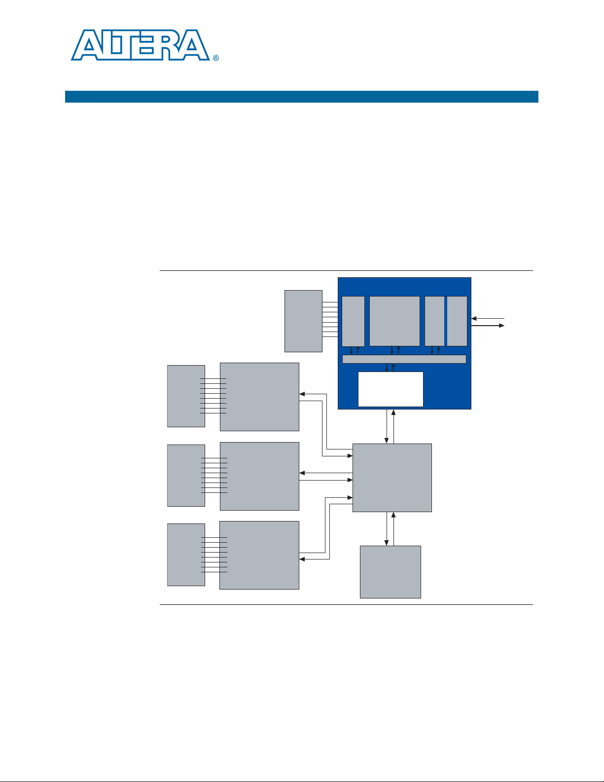
The RapidIO interconnect—an open standard developed by the RapidIO Trade
Association—is a high-performance packet-switched interconnect technology
designed to pass data and control information between microprocessors, digital signal
processors (DSPs), communications and network processors, system memories, and
peripheral devices.
The Altera
specification and targets high-performance, multi-computing, high-bandwidth, and
co-processing I/O applications. Figure 1–1 shows an example system
implementation.
Figure 1–1. Typical RapidIO Application
®
RapidIO II MegaCore® function complies with the RapidIO v2.2
Features
August 2014 Altera Corporation RapidIO II MegaCore Function
This section outlines the features and supported transactions of the RapidIO II IP core.
User Guide
Page 10

1–2 Chapter 1: About The RapidIO II MegaCore Function
Features
New Features in the RapidIO II IP Core v14.0 and v14.0 Arria 10 Edition Releases
The RapidIO II IP core v14.0 Arria 10 Edition adds the following new feature:
■ Support for Arria 10 devices
For details about changes to the IP core, refer to “Document Revision History” on
page Info–1. For an overview, refer to the RapidIO II IP core chapter in the Altera
MegaCore Library Release Notes. IP core variations that target an Arria 10 device have
additional interfaces and design requirements.
f For information about the new Altera IP design flow in the Quartus II software v14.0
and v14.0 Arria 10 Edition, which impacts all Altera IP cores, refer to the
“Introduction to Altera IP Cores” section in the “Managing Quartus II Projects”
chapter in Volume 1: Design and Synthesis of the Quartus II Handbook and to Introduction
to Altera IP Cores.
The RapidIO II IP core v13.0 and v13.1 do not add any new features.
RapidIO II IP Core Features
The RapidIO II IP core has the following features:
■ Compliant with the RapidIO Trade Association RapidIO Interconnect Specification,
Revision 2.2, June 2011, available from the RapidIO Trade Association website at
www.rapidio.org
■ Supports 8-bit or 16-bit device IDs
■ Supports incoming and outgoing multi-cast events
■ Provides a 128-bit wide Avalon Streaming (Avalon-ST) pass-through interface for
fully integrated implementation of custom user logic
RapidIO II MegaCore Function August 2014 Altera Corporation
User Guide
Page 11

Chapter 1: About The RapidIO II MegaCore Function 1–3
Features
■ Physical layer features
■ 1×/2×/4× serial with integrated transceivers
■ Fallback to 1× from 4× and 2× modes
■ Fallback to 2× from 4×
■ All five standard serial data rates supported: 1.25, 2.5, 3.125, 5.0 and
6.25 gigabaud (Gbaud)
■ Long control symbol
■ IDLE2 idle sequence
■ Extraction and insertion of command and status (CS) field
■ Support for software control of local and link-partner transmitter emphasis
■ Insertion of clock compensation sequences
■ Receive/transmit packet buffering, scrambling/descrambling, flow control,
error detection and recovery, packet assembly, and packet delineation
■ Automatic freeing of resources used by acknowledged packets
■ Automatic retransmission of retried packets
■ Scheduling of transmission, based on priority
■ Software support for ackID synchronization
■ Virtual channel (VC) 0 support
■ Reliable traffic (RT) support
■ Critical request flow (CRF) support
■ Transport layer features
■ Supports multiple Logical layer modules
■ Supports an Avalon Streaming (Avalon-ST) pass-through interface for custom
implementation of capabilities such as data streaming and message passing
■ A round-robin, priority-supporting outgoing scheduler chooses packets to
transmit from various Logical layer modules
■ Logical layer features
■ Generation and management of transaction IDs
■ Automatic response generation and processing
■ Response Request Timeout checking
■ Capability registers (CARs), command and status registers (CSRs), and Error
Management Extensions registers
■ Direct register access, either remotely or locally
■ Maintenance master and slave Logical layer modules
August 2014 Altera Corporation RapidIO II MegaCore Function
User Guide
Page 12

1–4 Chapter 1: About The RapidIO II MegaCore Function
Device Family Support
■ Input/Output Avalon
Logical layer modules with 128-bit wide datapath and burst support
■ Doorbell module supporting 16 outstanding
mechanism
■ Optional preservation of transaction order between outgoing
messages and I/O write requests
■ Registers and interrupt indicate NWRITE_R transaction completion
■ Preservation of transaction order between outgoing I/O read requests and I/O
write requests from Avalon-MM interfaces
■ Cycle-accurate simulation models for use in Altera-supported VHDL and Verilog
HDL simulators
■ IEEE-encrypted HDL simulation models for improved simulation efficiency
■ Support for OpenCore Plus evaluation
Supported Transactions
The RapidIO II IP core supports the following RapidIO transactions:
■
NREAD
request and response
■
NWRITE
request
®
Memory-Mapped (Avalon-MM) master and slave
DOORBELL
packets with time-out
DOORBELL
■
NWRITE_R
■
SWRITE
■
MAINTENANCE
■
MAINTENANCE
■
MAINTENANCE
■
DOORBELL
request
Device Family Support
Tab le 1– 1 defines the device support levels for Altera IP cores.
Table 1–1. Altera IP Core Device Support Levels
Preliminary support—The IP core is verified with preliminary timing models for this device family.
The IP core meets all functional requirements, but might still be undergoing timing analysis for the
device family. It can be used in production designs with caution.
Final support—The IP core is verified with final timing models for this device family. The IP core
meets all functional and timing requirements for the device family and can be used in production
designs.
request and response
read request and response
write request and response
port-write request
request and response
RapidIO II MegaCore Function August 2014 Altera Corporation
User Guide
Page 13

Chapter 1: About The RapidIO II MegaCore Function 1–5
IP Core Verification
Tab le 1– 2 shows the level of support offered by the RapidIO II IP core for each Altera
device family.
Table 1–2. Device Family Support
Device Family Support
Arria 10 Refer to the What’s New in Altera IP page of the Altera website.
Arria V (GX and GT) Final
Arria V GZ Final
Cyclone V Final
Stratix V Final
Other device families No support
IP Core Verification
Before releasing a publicly available version of the RapidIO II IP core, Altera runs a
comprehensive verification suite in the current version of the Quartus
These tests use standalone methods and the Qsys system integration tool to create the
instance files. These files are tested in simulation and hardware to confirm
functionality. Altera tests and verifies the RapidIO II MegaCore function in hardware
for different platforms and environments.
Altera also performs interoperability testing to verify the performance of the IP core
and to ensure compatibility with ASSP devices.
Simulation Testing
Altera verifies the RapidIO II IP core using the following industry-standard
simulators:
■ ModelSim
■ VCS
The test suite contains testbenches that use the Cadence Serial RapidIO Verification IP
(VIP), the Cadence Compliance Management System (CMS) implementation of the
RapidIO Trade Association interoperability checklist, and the RapidIO bus functional
model (BFM) from the RapidIO Trade Association to verify the functionality of the IP
core.
The test suite confirms various functions, including the following functionality:
®
simulator
®
II software.
■ Link initialization
■ Packet format
■ Packet priority
■ Error handling
■ Throughput
■ Flow control
August 2014 Altera Corporation RapidIO II MegaCore Function
User Guide
Page 14

1–6 Chapter 1: About The RapidIO II MegaCore Function
IP Core Verification
Constrained random techniques generate appropriate stimulus for the functional
verification of the IP core. Functional and code coverage metrics measure the quality
of the random stimulus, and ensure that all important features are verified.
Hardware Testing
Altera tests and verifies the RapidIO II IP core in hardware for different platforms and
environments.
The hardware tests cover serial 1x, 2x, and 4x variations running at 1.25, 2.5, 3.125, 5.0,
and 6.25 Gbaud, and processing the following traffic types:
■
NREAD
s of various payload sizes
■
NWRITE
■
NWRITE_R
■
SWRITE
■
Port-writes
■
DOORBELL
s of various payload sizes
s of various payload sizes
s of various payload sizes
messages
■
MAINTENANCE
reads and writes
The hardware tests also cover the following control symbol types:
■
Status
■
Packet-accepted
■
Packet-retry
■
Packet-not-accepted
■
Start-of-packet
■
End-of-packet
■
Link-request, Link-response
■
Stomp
■
Restart-from-retry
■
Multicast-event
Interoperability Testing
Altera performs interoperability tests on the RapidIO II IP core, which certify that the
RapidIO II IP core is compatible with third-party RapidIO devices.
Altera performs interoperability testing with processors and switches from various
manufacturers including:
■ Texas Instruments Incorporated
■ Integrated Device Technology, Inc. (IDT)
Altera has performed interoperability tests with the IDT CPS-1848 and IDT CPS-1616
switches. Testing of additional devices is an on-going process.
RapidIO II MegaCore Function August 2014 Altera Corporation
User Guide
Page 15

Chapter 1: About The RapidIO II MegaCore Function 1–7
Performance and Resource Utilization
Performance and Resource Utilization
This section contains tables showing IP core variation sizes in the different device
families. Ta bl e 1– 3 lists the resources and expected performance for selected
variations that use these modules:
■ Minimal variation:
■ Physical layer
■ Transport layer
■ Avalon-ST pass-through interface
■ Full-featured variation:
■ Physical layer
■ Transport layer
■ Maintenance module
■ Doorbell module
■ Input/Output Avalon-MM master
■ Input/Output Avalon-MM slave
■ Error Management Registers block
All variations are configured with the following parameter settings:
■ Transceiver reference clock frequency of 156.25 MHz
■ The maximum RapidIO baud rate supported by the device
■ Support 1×, 2×, and 4× modes of operation
The numbers of ALMs, primary logic registers, and secondary logic registers in
Tab le 1– 3 are rounded up to the nearest 100.
Tab le 1– 3 shows results obtained using the Quartus II software v12.1 SP1 or Quartus
II software v14.0 Arria 10 Edition for the following devices:
■ Arria 10 (10AX048E2F29E2LG) (v14.0 Arria 10 Edition)
■ Arria V (5AGXFB3H4F35I5) (v12.1 SP1)
■ Cyclone V (5CGXFC7C6U19I7) (v12.1 SP1)
■ Stratix V (5SGXEA7H3F35C3) (v12.1 SP1)
Table 1–3. RapidIO II IP Core FPGA Resource Utilization (Part 1 of 2)
Parameters
Device
ALMs
Variation Baud Rate (Gbaud) Primary Secondary
Minimal 6.25 14300 14300 1100 31
Arria 10
Arria V
Full-featured 6.25 20300 25300 1900 49
Minimal
Full-featured 24400 27500 2700 68
6.25
14800 13800 1700 41
Registers Memory
Blocks
(M10K or
(1)
M20K
)
August 2014 Altera Corporation RapidIO II MegaCore Function
User Guide
Page 16

1–8 Chapter 1: About The RapidIO II MegaCore Function
Device Speed Grades
Table 1–3. RapidIO II IP Core FPGA Resource Utilization (Part 2 of 2)
Parameters
Device
Variation Baud Rate (Gbaud) Primary Secondary
Cyclone V
Full-featured 24500 27500 0 68
Minimal
Minimal
Stratix V
Note to Table 1–3:
(1) M10K for Arria V and Cyclone V devices and M20K for Stratix V devices.
Full-featured 24100 28000 2400 55
3.125
6.25
ALMs
14800 13800 0 41
14300 13800 1300 33
Registers Memory
Blocks
(M10K or
M20K
Device Speed Grades
Tab le 1– 4 shows the recommended device family speed grades for the supported link
widths and internal clock frequencies.
Table 1–4. Recommended Device Family and Speed Grades
Rate 1.25 Gbaud
Device Family
f
MAX
31.25 MHz 62.50 MHz 78.125 MHz
Arria 10 –1, –2, –3 –1, –2, –3 –1, –2, –3 –1, –2, –3 –1, –2
Arria V –4, –5, –6 –4, –5, –6 –4, –5, –6 –4, –5 –4, –5
Arria V GZ –3, –4 –3, –4 –3, –4 –3, –4 –3, –4
Cyclone V –6, –7 –6, –7 –6, –7 –7
Stratix V –2, –3, –4 –2, –3, –4 –2, –3, –4 –2, –3, –4 –2, –3, –4
Notes to Table 1–4:
(1) In this table, the entry –n indicates that both the industrial speed grade In and the commercial speed grade Cn are supported for this device
family and baud rate.
(2) In the Cyclone V device family, only Cyclone V GT devices support the 5.0 GBaud rate.
(1)
2.5
Gbaud
3.125 Gbaud
5.0
Gbaud
125
MHz
(2)
6.25
Gbaud
156.25 MHz
—
(1)
)
Release Information
Tab le 1– 5 provides information about this release of the RapidIO II IP core.
Table 1–5. RapidIO Release Information
Item Description
Version 14.0 14.0 Arria 10 Edition
Release Date June 2014 August 2014
Ordering Code IP-RAPIDIOII
Product ID 0108
Vendor ID 6AF7
RapidIO II MegaCore Function August 2014 Altera Corporation
User Guide
Page 17

Chapter 1: About The RapidIO II MegaCore Function 1–9
<path>
common
Contains shared components
altera_rapidio2
Contains the RapidIO II MegaCore function files
Installation directory
ip
Contains the Altera MegaCore IP Library and third-party IP cores
altera
Contains the Altera MegaCore IP Library
Installation and Licensing
Altera verifies that the current version of the Quartus II software compiles the
previous version of each IP core. Any exceptions to this verification are reported in the
MegaCore IP Library Release Notes and in the Altera RapidIO II IP core errata. Altera
does not verify compilation with IP core versions older than the previous release.
Installation and Licensing
The RapidIO II IP core is part of the Altera MegaCore IP Library, which is distributed
with the Quartus II software and downloadable from the Altera website,
www.altera.com.
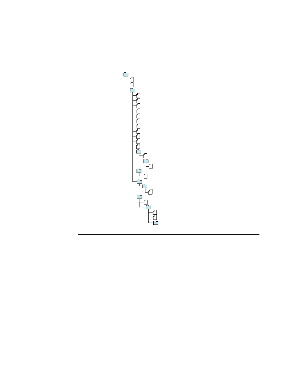
Figure 1–2 shows the directory structure after you install the RapidIO II IP core,
where
<
path> is the installation directory. The default installation directory on
Windows is C:\altera\<version number>; on Linux it is /opt/altera<version number>.
Figure 1–2. Directory Structure
You can use Altera’s free OpenCore Plus evaluation feature to evaluate the IP core in
simulation and in hardware before you purchase a license. You must purchase a
license for the IP core only when you are satisfied with its functionality and
performance, and you want to take your design to production.
After you purchase a license for the RapidIO II IP core, you can request a license file
from the Altera website at www.altera.com/licensing and install it on your computer.
When you request a license file, Altera emails you a license.dat file. If you do not have
internet access, contact your local Altera representative.
OpenCore Plus Evaluation
With the Altera free OpenCore Plus evaluation feature, you can perform the following
actions:
■ Simulate the behavior of a megafunction (Altera IP core or AMPP
megafunction) in your system using the Quartus II software and Altera-supported
VHDL and Verilog HDL simulators.
■ Verify the functionality of your design and evaluate its size and speed quickly and
easily.
■ Generate time-limited device programming files for designs that include IP cores.
■ Program a device and verify your design in hardware.
SM
August 2014 Altera Corporation RapidIO II MegaCore Function
User Guide
Page 18

1–10 Chapter 1: About The RapidIO II MegaCore Function
Installation and Licensing
OpenCore Plus Time-Out Behavior
OpenCore Plus hardware evaluation supports the following two operation modes:
■ Untethered—the design runs for a limited time.
■ Tethered—requires a connection between your board and the host computer. If
tethered mode is supported by all megafunctions in a design, the device can
operate for a longer time or indefinitely.
All megafunctions in a device time out simultaneously when the most restrictive
evaluation time is reached. If there is more than one megafunction in a design, a
specific megafunction's time-out behavior may be masked by the time-out behavior of
the other megafunctions.
1 For Altera IP cores, the untethered time-out is 1 hour; the tethered time-out value is
indefinite.
After the hardware evaluation time expires, the RapidIO II IP core behaves as if its
reset signal were held asserted, and your design stops working.
f
For Information About Refer To
Installation and licensing Altera Software Installation and Licensing
Open Core Plus AN 320: OpenCore Plus Evaluation of Megafunctions
RapidIO II MegaCore Function August 2014 Altera Corporation
User Guide
Page 19

You can customize the RapidIO II IP core to support a wide variety of applications.
When you generate the IP core you can choose whether or not to generate a
simulation model. If you generate a simulation model, Altera provides a Verilog
testbench customized for your IP core variation. If you specify a VHDL simulation
model, you must use a mixed-language simulator to run the testbench, or create your
own VHDL-only simulation environment.
Customizing and Generating IP Cores
You can customize IP cores to support a wide variety of applications. The Quartus II
IP Catalog displays IP cores available for the current target device. The parameter
editor guides you to set parameter values for optional ports, features, and output files.
To customize and generate a custom IP core variation, follow these steps:
1. In the IP Catalog (Tools > IP Catalog), locate and double-click the name of the IP
core to customize. The parameter editor appears.
2. Getting Started
2. Specify a top-level name for your custom IP variation. This name identifies the IP
core variation files in your project. If prompted, also specify the target Altera
device family and output file HDL preference. Click OK.
3. Specify the desired parameters, output, and options for your IP core variation:
■ Optionally select preset parameter values. Presets specify all initial parameter
values for specific applications (where provided).
■ Specify parameters defining the IP core functionality, port configuration, and
device-specific features.
■ Specify options for generation of a timing netlist, simulation model, testbench,
or example design (where applicable).
■ Specify options for processing the IP core files in other EDA tools.
4. Click Finish or Generate to generate synthesis and other optional files matching
your IP variation specifications. The parameter editor generates the top-level .qip
or .qsys IP variation file and HDL files for synthesis and simulation. Some IP cores
also simultaneously generate a testbench or example design for hardware testing.
When you generate the IP variation with a Quartus II project open, the parameter
editor automatically adds the IP variation to the project. Alternatively, click Project >
Add/Remove Files in Project to manually add a top-level .qip or .qsys IP variation
file to a Quartus II project. To fully integrate the IP into the design, make appropriate
pin assignments to connect ports. You can define a virtual pin to avoid making
specific pin assignments to top-level signals.
August 2014 Altera Corporation RapidIO II MegaCore Function
User Guide
Page 20

2–2 Chapter 2: Getting Started
IFiles Generated for Altera IP Cores (Legacy Parameter Editor)
IFiles Generated for Altera IP Cores (Legacy Parameter Editor)
The Quartus II software version 14.0 and previous parameter editor generates the
following output file structure for Altera IP cores:
Figure 2–1. IP Core Generated Files (Legacy Parameter Editor)
<Project Directory>
<your_ip>.qip - Quartus II IP integration file
<your_ip>.v, .sv. or .vhd - Top-level IP synthesis file
<your_ip> - IP core synthesis files
<your_ip>.sv, .v, or .vhd - HDL synthesis files
<your_ip>.sdc - Timing constraints file
<your_ip>.bsf - Block symbol schematic file
<your_ip>.cmp - VHDL component declaration file
<your_ip>_syn.v or .vhd - Timing & resource estimation netlist
<your_ip>.sip - Lists files for simulation
<your_ip>.ppf - XML I/O pin information file
<your_ip>.spd - Combines individual simulation scripts
<your_ip>_sim.f - Refers to simulation models and scripts
<your_ip>_sim
<Altera IP_name>_instance
<your_ip>_testbench or _example - testbench or example design
Notes:
1. If supported and enabled for your IP variation
2. If functional simulation models are generated
1
<Altera IP>_instance.vo - IPFS model
<simulator_vendor>
<simulator setup scripts>
1
2
1
1
1
1
In the case of the RapidIO II IP core you generate from the Quartus II IP Catalog in the
Quartus II software v14.0 Arria 10 Edition:
■ The testbench script appears in <your_ip>_sim/<vendor>.
■ The testbench files appear in <your_ip>_sim/altera_rapidio2/tb.
■ The IP core simulation files appear in <your_ip>_sim/altera_rapidio2/<vendor>.
The RapidIO II IP core does not generate an example design.
RapidIO II MegaCore Function August 2014 Altera Corporation
User Guide
Page 21

Chapter 2: Getting Started 2–3
Notes:
1. If supported and enabled for your IP variation
2. If functional simulation models are generated
<Project Directory>
<your_ip>_bb.v - Verilog HDL black box EDA synthesis file
<your_ip>_inst.v or .vhd - Sample instantiation template
synthesis - IP synthesis files
<your_ip>.qip - Lists files for synthesis
testbench - Simulation testbench files
1
<testbench_hdl_files>
<simulator_vendor> - Testbench for supported simulators
<simulation_testbench_files>
<your_ip>.v or .vhd - Top-level IP variation synthesis file
simulation - IP simulation files
<your_ip>.sip - NativeLink simulation integration file
<simulator vendor> - Simulator setup scripts
<simulator_setup_scripts>
<your_ip> - IP core variation files
<your_ip>.qip or .qsys - System or IP integration file
<your_ip>_generation.rpt - IP generation report
<your_ip>.bsf - Block symbol schematic file
<your_ip>.ppf - XML I/O pin information file
<your_ip>.spd - Combines individual simulation startup scripts
1
<your_ip>.html - Contains memory map
<your_ip>.sopcinfo - Software tool-chain integration file
<your_ip>_syn.v or .vhd - Timing & resource estimation netlist
1
<your_ip>.debuginfo - Lists files for synthesis
<your_ip>.v, .vhd, .vo, .vho - HDL or IPFS models
2
<your_ip>_tb - Testbench for supported simulators
<your_ip>_tb.v or .vhd - Top-level HDL testbench file
IFiles Generated for Altera IP Cores by Qsys (Legacy Parameter Editor)
IFiles Generated for Altera IP Cores by Qsys (Legacy Parameter Editor)
Generation of the IP core from Qsys produces the following output in Quartus II
software version 14.0 and previous.
Figure 2–2. IP Core Generated Files (Legacy Parameter Editor)
August 2014 Altera Corporation RapidIO II MegaCore Function
In the case of the RapidIO II IP core you generate from the Qsys IP Catalog in the
Quartus II software v14.0:
■ The testbench script appears in <Qsys system>/simulation/<vendor>.
■ The testbench files appear in <Qsys system>/simulation/submodules/tb.
■ The IP core simulation files appear in
The RapidIO II IP core does not generate an example design.
<Qsys system>/simulation/submodules/<vendor>.
User Guide
Page 22
2–4 Chapter 2: Getting Started
Files Generated for Altera IP Cores
Files Generated for Altera IP Cores
The Quartus II software version 14.0 Arria 10 Edition and later generates the
following output file structure for Altera IP cores:
Figure 2–3. IP Core Generated Files
<Project Directory>
<your_ip>.qsys - System or IP integration file
<your_ip>.sopcinfo - Software tool-chain integration file
<your_ip> - IP core variation files
<your_ip>.cmp - VHDL component declaration file
<your_ip>_bb.v - Verilog HDL black box EDA synthesis file
<your_ip>_inst.v or .vhd - Sample instantiation template
<your_ip>.ppf - XML I/O pin information file
<your_ip>.qip - Lists IP synthesis files
<your_ip>.sip - Lists files for simulation
<your_ip>_generation.rpt - IP generation report
<your_ip>.debuginfo - IP generation report
<your_ip>.html - Contains memory map
<your_ip>.bsf - Block symbol schematic
<your_ip>.spd - Combines individual simulation startup scripts
sim - IP simulation files
<your_ip>.v or .vhd - Top-level simulation file
<EDA_tool_name> - Simulator setup scripts
<simulator_setup_scripts>
synth - IP synthesis files
<your_ip>.v or .vhd - Top-level IP synthesis file
<IP subcore library> - IP subcore files
sim
<HDL files>
<your_testbench>_tb - Simulation testbench files
<your_ip>_tb.qsys - Testbench system file
<your_testbench>_tb
1. If supported and enabled for your IP variation
1
<your_testbench>_tb.csv
<your_testbench>_tb.spd
sim - IP core simulation files
1
1
In the case of the RapidIO II IP core you generate in the Quartus II software v14.0
Arria 10 Edition:
■ The testbench script appears in <Qsys_system or your_ip>/sim/<vendor>.
■ The testbench files appear in
<Qsys_system or your_ip>/altera_rapidio2_140/sim/tb.
■ The IP core simulation files appear in
<Qsys_system or your_ip>/altera_rapidio2_140/sim/<vendor>.
The RapidIO II IP core does not generate an example design.
Simulating IP Cores
The Quartus II software supports RTL- and gate-level design simulation of Altera IP
cores in supported EDA simulators. Simulation involves setting up your simulator
working environment, compiling simulation model libraries, and running your
simulation.
RapidIO II MegaCore Function August 2014 Altera Corporation
User Guide
Page 23

Chapter 2: Getting Started 2–5
Simulating IP Cores
You can use the functional simulation model and the testbench or example design
generated with your IP core for simulation. The functional simulation model and
testbench files are generated in a project subdirectory. This directory may also include
scripts to compile and run the testbench. For a complete list of models or libraries
required to simulate your IP core, refer to the scripts generated with the testbench.
You can use the Quartus II NativeLink feature to automatically generate simulation
files and scripts. NativeLink launches your preferred simulator from within the
Quartus II software.
For more information about simulating Altera IP cores, refer to Simulating Altera
Designs in volume 3 of the Quartus II Handbook.
Simulating the Testbench with the ModelSim Simulator
To simulate the RapidIO II IP core testbench using the Mentor Graphics ModelSim
simulator, perform the following steps:
1. Start the ModelSim simulator.
2. In ModelSim, change directory to the directory where the testbench simulation
script is located:
■ For Arria 10 variations, change directory to <variation>/sim/mentor.
■ For all other variations you generate from the Quartus II IP Catalog, change
directory to <variation>_sim/mentor.
■ For all other variations you generate from the Qsys IP Catalog, change
directory to <Qsys system>/simulation/mentor.
3. To set up the required libraries, compile the generated simulation model, and
exercise the simulation model with the provided testbench, type one of the
following sets of commands:
a. For non-Arria 10 variations, type the following commands:
do msim_setup.tcl
set TOP_LEVEL_NAME <variation>.tb_rio (
ld
run -all
b. For Arria 10 variations, type the following commands:
do msim_setup.tcl
set TOP_LEVEL_NAME <variation>_altera_rapidio2_140.tb_rio
ld
run -all
August 2014 Altera Corporation RapidIO II MegaCore Function
User Guide
Page 24

2–6 Chapter 2: Getting Started
Integrating Your IP Core in Your Design
Simulating the Testbench with the VCS Simulator
To simulate the RapidIO II IP core testbench using the Synopsys VCS simulator,
perform the following steps:
1. Change directory to the directory where the testbench simulation script is located:
■ For Arria 10 variations, change directory to <variation>/sim/synopsys/vcs.
■ For all other variations you generate from the Quartus II IP Catalog, change
directory to <variation>_sim/synopsys/vcs.
■ For all other variations you generate from the Qsys IP Catalog, change
directory to <Qsys system>/simulation/synopsys/vcs
2. Type the following commands:
sh vcs_setup.sh TOP_LEVEL_NAME="tb_rio"
./simv
f
Quartus II software See the Quartus II Help topics:
IP Catalog
Altera simulation models
For Information About Refer To
Integrating Your IP Core in Your Design
When you integrate your IP core instance in your design, you must pay attention to
some additional requirements. If you generate your IP core from the Qsys IP catalog
and build your design in Qsys, you can perform these steps in Qsys. If you generate
your IP core directly from the Quartus II IP catalog, you must implement these steps
manually in your design.
Dynamic Transceiver Reconfiguration Controller for Arria V, Arria V GZ, Cyclone V, and Stratix V Variations
RapidIO II IP core variations that target an Arria V, Arria V GZ, Cyclone V, or Stratix
V device require an external reconfiguration controller to function correctly in
hardware. RapidIO II IP core variations that target an Arria 10 device include a
reconfiguration controller block and do not require an external reconfiguration
controller. However, you need to control dynamic transceiver reconfiguration in Arria
10 devices through the Arria 10 dynamic reconfiguration interface if you turn on that
interface in the RapidIO II parameter editor.
“About the Quartus II Software”
“About the IP Catalog”
Simulating Altera Designs chapter in volume 3 of
the Quartus II Handbook
Keeping the reconfiguration controller external to the IP core in these devices
provides the flexibility to share the reconfiguration controller among multiple IP cores
and to accommodate FPGA transceiver layouts based on the usage model of your
application. In Arria 10 devices, you can configure individual transceiver channels
flexibly through an Avalon-MM Arria 10 transceiver reconfiguration interface.
RapidIO II MegaCore Function August 2014 Altera Corporation
User Guide
Page 25

Chapter 2: Getting Started 2–7
Integrating Your IP Core in Your Design
Altera recommends that you implement the reconfiguration controller with an Altera
Transceiver Reconfiguration Controller. The Transceiver Reconfiguration Controller
performs offset cancellation during bring-up of the transceiver channels.
The Transceiver Reconfiguration Controller is available in the IP catalog. You must
add it to your design and connect it to the RapidIO II IP core reconfiguration signals.
In the Transceiver Reconfiguration Controller parameter editor, you select the features
of the transceiver that can be dynamically reconfigured. However, you must ensure
that the following two features are turned on:
■ Enable PLL calibration
■ Enable Analog controls
An informational message in the RapidIO II parameter editor tells you the number of
reconfiguration interfaces you must configure in your dynamic reconfiguration block.
You must configure the Transceiver Reconfiguration Controller Number of
reconfiguration interfaces parameter with this value. For more information, refer to
Table 5–7 on page 5–5.
The Reconfiguration Controller communicates with the RapidIO II IP core on two
busses:
■
reconfig_to_xcvr
■
reconfig_from_xcvr
(output)
(input)
Each of these busses connects to the bus of the same name in the RapidIO II IP core.
You must also connect the following Reconfiguration Controller signals:
■
mgmt_clk_clk
■
mgmt_rst_reset
■
reconfig_busy
f For information about the Altera Transceiver Reconfiguration Controller, refer to the
Altera Transceiver PHY IP Core User Guide.
Transceiver PHY Reset Controller
You must add an Altera Transceiver PHY Reset Controller IP core to your design, and
connect it to the RapidIO II IP core reset signals. This block implements a reset
sequence that resets the device transceivers correctly. The default parameter settings
of the Altera Transceiver PHY Reset Controller IP core are compatible with the
RapidIO II IP core requirements. For more information, refer to “Reset for RapidIO II
IP Cores” on page 4–4.
f For information about the Altera Transceiver PHY Reset Controller IP core, refer to
the Altera Transceiver PHY IP Core User Guide or the Arria 10 Transceiver PHY User
Guide.
August 2014 Altera Corporation RapidIO II MegaCore Function
User Guide
Page 26

2–8 Chapter 2: Getting Started
Integrating Your IP Core in Your Design
Transceiver Settings
Altera recommends that you maintain the default Native PHY IP core settings
generated for the RapidIO II IP core. If you edit the existing Native PHY IP core, the
regenerated Native PHY IP core does not instantiate correctly in the top-level
RapidIO II IP core. If you must modify transceiver settings, perform the modifications
by editing the project Quartus Settings File (.qsf).
Adding Transceiver Analog Settings for Arria V GZ and Stratix V Variations
In general, Altera recommends that you maintain the default transceiver settings
specified by the RapidIO II IP core. However, Arria V GZ or Stratix V variations
require that you specify some analog transceiver settings.
After you generate your RapidIO II IP core in a Quartus II project that targets an
Arria V GZ or Stratix V device, perform the following steps:
1. In the Quartus II software, on the Assignments tab, click Assignment Editor.
2. In the Assignment Editor, in the Assignment Name column, double click
<<new>> and select Transceiver Analog Settings Protocol.
3. In the To column, type the name of the transceiver serial data input node in your
IP core variation. This name is the variation-specific version of the
rd
signal.
4. In the Va l u e column, click and select SRIO.
5. Repeat steps 2 to 4 to create an additional assignment, with the following
substitution:
In step 3, instead of typing the name of the transceiver serial data input node, type
the name of the transceiver serial data output put node. This name is the
variation-specific version of the
External Transceiver PLL
RapidIO II IP cores that target an Arria 10 device require an external TX transceiver
PLL to compile and to function correctly in hardware. You must instantiate and
connect this IP core to the RapidIO II IP core.
You can create an external transceiver PLL from the IP Catalog. Select the ATX PLL IP
core or the fPLL IP core. In the ATX TX PLL parameter editor, set the following
parameter values:
■ Set PLL output frequency to one half the value you select for the Maximum baud
rate parameter in the RapidIO II parameter editor. The transceiver performs dual
edge clocking, using both the rising and falling edges of the input clock from the
PLL. Therefore, this PLL output frequency setting supports the customer-selected
maximum data rate on the RapidIO link.
■ Set PLL reference clock frequency to the value you select for the Reference clock
frequency parameter in the RapidIO II parameter editor.
td
signal.
■ Turn o n Include Master Clock Generation Block.
■ Turn o n Enable bonding clock output ports.
■ Set PMA interface width to 20.
RapidIO II MegaCore Function August 2014 Altera Corporation
User Guide
Page 27

Chapter 2: Getting Started 2–9
Compiling the Full Design and Programming the FPGA
When you generate a RapidIO II IP core, the Quartus II software also generates the
HDL code for an ATX PLL, in the file
<variation>/altera_xcvr_atx_pll_a10_140/synth/altera_rapidio2_pll.v. However, the
HDL code for the RapidIO II IP core does not instantiate the ATX PLL. If you choose
to use the ATX PLL provided with the RapidIO II IP core, you must instantiate and
connect the ATX PLL instance with the RapidIO II IP core in user logic.
You must connect the TX PLL IP core to the RapidIO II IP core according to the
following rules.
Table 2–1. External Transceiver TX PLL Connections to RapidIO II IP Core
Signal Direction Connection Requirements
pll_refclk0
tx_bonding_clocks
[(6 x <number of
lanes>)–1:0]
Input
Output
Drive the PLL
IP core
source. The minimum allowed frequency for the
pll_refclk0
Connect
tx_bonding_clocks_chN
channel N, for each transceiver channel N that connects to
the RapidIO link. The transceiver channel input ports are
RapidIO II IP core input ports.
pll_refclk0
tx_pll_refclk
clock in an Arria 10 ATX PLL is 100 MHz.
tx_bonding_clocks[6n+5:6n]
input port and the RapidIO II
signal from the same clock
input bus of transceiver
to the
For an example of how to configure and connect a TX PLL IP core to the other system
components, such as the external reset controller, refer to the cleartext testbench files
and Chapter 7, Testbench, especially Figure 7–2.
f For information about the connection requirements and options, refer to the Arria 10
Transceiver PHY User Guide.
Compiling the Full Design and Programming the FPGA
You can use the Start Compilation command on the Processing menu in the
Quartus II software to compile your design. After successfully compiling your design,
program the targeted Altera device with the Programmer and verify the design in
hardware.
1 Before compiling your design in the Quartus II software, you must perform the
modifications described in “Adding Transceiver Analog Settings for Arria V GZ and
Stratix V Variations” on page 2–8.
f
For Information About Refer To
Compiling your design
Programming the device
Quartus II Incremental Compilation for Hierarchical and TeamBased Design chapter in volume 1 of the Quartus II Handbook
Device Programming section in volume 3 of the Quartus II
Handbook
August 2014 Altera Corporation RapidIO II MegaCore Function
User Guide
Page 28

2–10 Chapter 2: Getting Started
Instantiating Multiple RapidIO II IP Cores
Instantiating Multiple RapidIO II IP Cores
If you want to instantiate multiple RapidIO II IP cores that target an Arria V, Arria V
GZ, Cyclone V, or Stratix V device, a few additional steps are required. These steps are
not relevant for variations that target an Arria 10 device.
The Arria V, Arria V GZ, Cyclone V, and Stratix V transceivers are configured with the
Altera Native PHY IP core. When your design contains multiple RapidIO II IP cores,
the Quartus II Fitter handles the merge of multiple Native PHY IP cores in the same
transceiver block automatically, if they meet the merging requirements specified in
the Altera Transceiver PHY IP Core User Guide.
If you have different RapidIO II IP cores in different transceiver blocks on your
device, you may choose to include multiple Transceiver Reconfiguration Controllers
in your design. However, you must ensure that the Transceiver Reconfiguration
Controllers that you add to your design have the correct number of interfaces to
control dynamic reconfiguration of all your RapidIO II IP core transceivers. The
correct total number of reconfiguration interfaces is the sum of the reconfiguration
interfaces for each RapidIO II IP core; the number of reconfiguration interfaces for
each RapidIO II IP core is the number of channels plus one. You must ensure that the
reconfig_togxb
connect to a single Transceiver Reconfiguration Controller.
and
reconfig_fromgxb
signals of an individual RapidIO II IP core
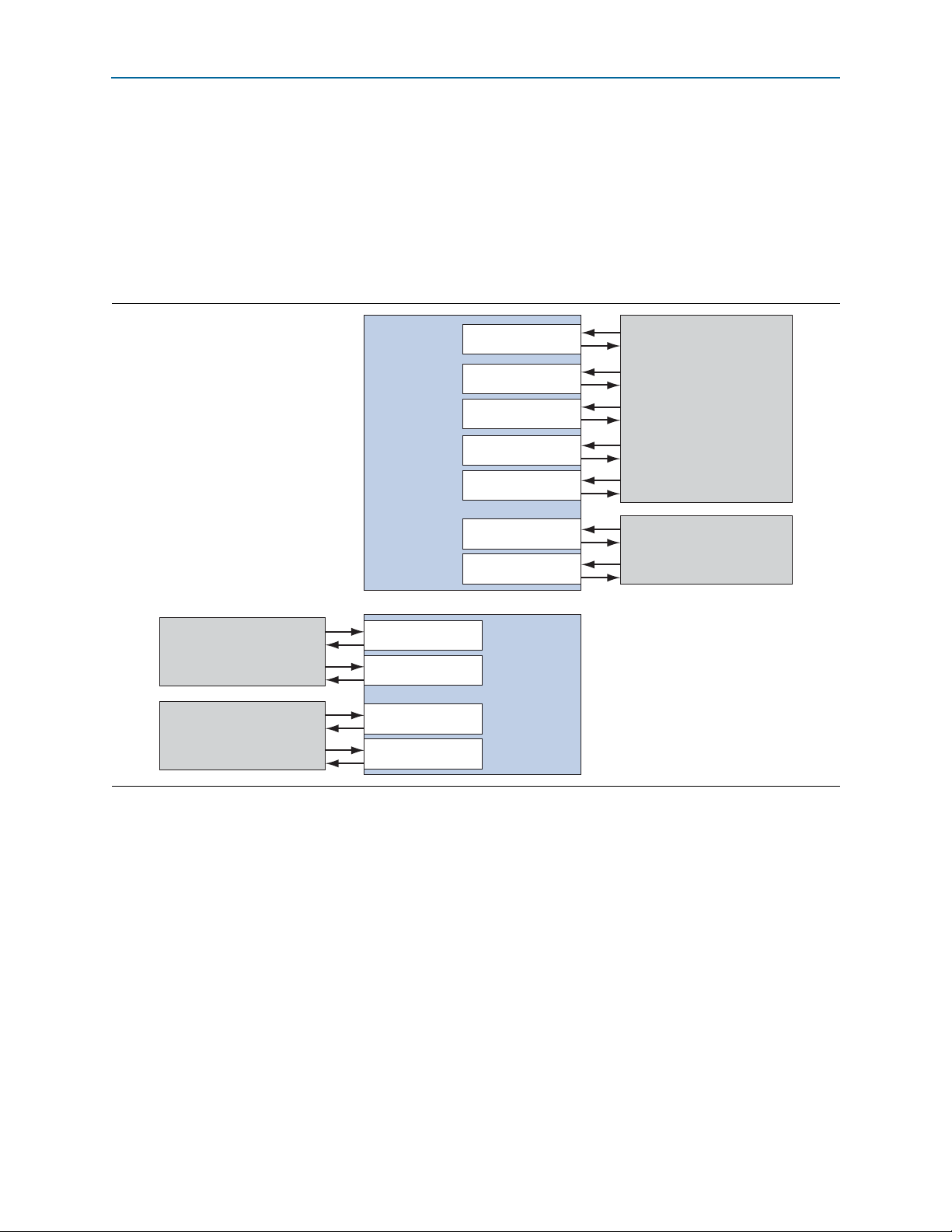
For example, if your design includes one ×4 RapidIO II IP core and three ×1
RapidIO II IP cores, the Transceiver Reconfiguration Controllers in your design must
include eleven dynamic reconfiguration interfaces: five for the ×4 RapidIO II IP core,
and two for each of the ×1 RapidIO II IP cores. The dynamic reconfiguration interfaces
connected to a single RapidIO II IP core must belong to the same Transceiver
Reconfiguration Controller. In most cases, your design has only a single Transceiver
Reconfiguration Controller, which has eleven dynamic reconfiguration interfaces. If
you choose to use two Transceiver Reconfiguration Controllers, for example, to
accommodate placement and timing constraints for your design, each of the
RapidIO II IP cores must connect to a single Transceiver Reconfiguration Controller.
RapidIO II MegaCore Function August 2014 Altera Corporation
User Guide
Page 29
Chapter 2: Getting Started 2–11
Altera
Transceiver
Reconfiguration
Controller
0
x1 RapidIO II
IP Core
x1 RapidIO II
IP Core
Altera
Transceiver
Reconfiguration
Controller
1
reconfig_from_xcvr[N-1:0]
reconfig_to_xcvr[M-1:0]
reconfig_fromgxb[N-1:0]
reconfig_togxb[M-1:0]
reconfig_from_xcvr[N-1:0]
reconfig_to_xcvr[M-1:0]
reconfig_fromgxb[2N-1:N]
reconfig_togxb[2M-1:M]
reconfig_from_xcvr[N-1:0]
reconfig_to_xcvr[M-1:0]
reconfig_fromgxb[N-1:0]
reconfig_togxb[M-1:0]
reconfig_from_xcvr[N-1:0]
reconfig_to_xcvr[M-1:0]
reconfig_from_xcvr[N-1:0]
reconfig_to_xcvr[M-1:0]
reconfig_from_xcvr[N-1:0]
reconfig_to_xcvr[M-1:0]
reconfig_from_xcvr[N-1:0]
reconfig_to_xcvr[M-1:0]
reconfig_from_xcvr[N-1:0]
reconfig_to_xcvr[M-1:0]
reconfig_from_xcvr[N-1:0]
reconfig_to_xcvr[M-1:0]
reconfig_from_xcvr[N-1:0]
reconfig_to_xcvr[M-1:0]
reconfig_from_xcvr[N-1:0]
reconfig_to_xcvr[M-1:0]
reconfig_fromgxb[2N-1:N]
reconfig_togxb[2M-1:M]
x1 RapidIO II
IP Core
reconfig_fromgxb[N-1:0]
reconfig_togxb[M-1:0]
reconfig_fromgxb[2N-1:N]
reconfig_togxb[2M-1:M]
x4 RapidIO II
IP Core
reconfig_fromgxb[5N-1:4N]
reconfig_togxb[5M-1:4M]
reconfig_fromgxb[3N-1:2N]
reconfig_togxb[3M-1:2M]
reconfig_fromgxb[4N-1:3N]
reconfig_togxb[4M-1:3M]
reconfig_fromgxb[N-1:0]
reconfig_togxb[M-1:0]
reconfig_fromgxb[2N-1:N]
reconfig_togxb[2M-1:M]
Instantiating Multiple RapidIO II IP Cores
Figure 2–4 illustrates an example design with two Transceiver Reconfiguration
Controllers and four RapidIO II IP cores. In the example, Altera Transceiver
Reconfiguration Controller 0 has seven reconfiguration interfaces, and Altera
Transceiver Reconfiguration Controller 1 has four reconfiguration interfaces. Each
sub-block shown in a Transceiver Reconfiguration Controller block represents a single
reconfiguration interface. The example shows only one possible configuration for this
combination of RapidIO II IP cores; subject to the constraints described, you may
choose a different configuration.
Figure 2–4. Example Connections Between Two Transceiver Reconfiguration Controllers and Four RapidIO II IP Cores
August 2014 Altera Corporation RapidIO II MegaCore Function
Refer to Table 5–7 on page 5–5 for the values of N and M in Figure 2–4.
f Refer to the "Transceiver Reconfiguration Controller" chapter of the Altera Transceiver
PHY IP Core User Guide for more information about the Transceiver Reconfiguration
Controller interfaces for Arria V, Arria V GZ, Cyclone V, and Stratix V devices and
how to control dynamic reconfiguration for multiple transceiver channels. Refer to
Table 5–7 on page 5–5 for information about the
reconfig_to_xcvr
Transceiver Reconfiguration Controller interfaces of the same Transceiver
Reconfiguration Controller.
signals that connect a single RapidIO II IP core to multiple
reconfig_from_xcvr
and
User Guide
Page 30

2–12 Chapter 2: Getting Started
Instantiating Multiple RapidIO II IP Cores
RapidIO II MegaCore Function August 2014 Altera Corporation
User Guide
Page 31

3. Parameter Settings
You customize the RapidIO II IP core by specifying parameters in the RapidIO II
parameter editor, which you access from the MegaWizard Plug-In Manager or the
Qsys system integration tool in the Quartus II software.
This chapter describes the parameters and how they affect the behavior of the IP core.
Each section corresponds to a tab in the RapidIO II parameter editor.
In the RapidIO II parameter editor, you use the following tabs to parameterize the
RapidIO II IP core:
■ Physical Layer
■ Tra n s p or t L a ye r
■ Logical Layer
■ Capability Registers
■ Command and Status Registers
■ Error Management Registers
Physical Layer Settings
The Physical layer includes RapidIO II specific logic configuration and transceiver
configuration.
The RapidIO II IP core instantiates a Native PHY IP core to configure the transceivers.
The RapidIO II IP core provides no parameters to modify this configuration directly.
Altera recommends you do not modify the default transceiver settings configured in
the Native PHY IP core instance generated with the RapidIO II IP core.
f For information about the transceiver block, refer to Volume 3: Transceivers of the
Arria V Device Handbook, to Volume 2: Transceivers of the Cyclone V Device Handbook, or
to Volume 3: Transceivers of the Stratix V Device Handbook. For information about the
Native PHY IP core, refer to the Altera Transceiver PHY IP Core User Guide.
The Physical Layer parameters define the following characteristics of the Physical
layer:
■ Supported modes
■ Maximum baud rate
■ Reference clock frequency
■ Enable transceiver dynamic reconfiguration (Arria 10 variations only)
August 2014 Altera Corporation RapidIO II MegaCore Function
User Guide
Page 32

3–2 Chapter 3: Parameter Settings
Physical Layer Settings
Supported Modes
The Supported modes parameter allows you to specify which of the 1x, 2x, and 4x
modes of operation this RapidIO II IP core supports. All RapidIO II IP core variations
support 1x mode. The RapidIO II MegaCore function initially attempts link
initialization in the maximum number of lanes that the variation supports. The IP core
supports fallback to lower numbers of ports.
Maximum Baud Rate
Maximum baud rate defines the maximum supported baud rate. The RapidIO II IP
core does not support automatic baud rate discovery.
Tab le 3– 1 shows the baud rates supported by the RapidIO II IP core for each device
family. A device family may include devices at speed grades that do not support all
the indicated baud rates. For information about the speed grades the RapidIO II IP
core supports for each device family, RapidIO mode, and baud rate combination, refer
to Table 1–4 on page 1–8.
Table 3–1. RapidIO II IP Core Device Support
Mode 1x, 2x 4x
Device
Family
Arria 10 vvvvvvvvvv
Arria V vvvvvvvvvv
Cyclone V vvvv
Stratix V vvvvvvvvvv
Note to Tab le 3– 1:
(1) In the Cyclone V device family, only Cyclone V GT devices support the 5.0 GBaud rate.
Baud
Rate
(MBaud)
1250 2500 3125 5000 6250 1250 2500 3125 5000 6250
(1)
— vvvv
(1)
—
Reference Clock Frequency
Reference clock frequency defines the frequency of the reference clock for your
RapidIO II IP core internal transceiver. The RapidIO II parameter editor allows you to
select any frequency supported by the transceiver.
For more information about the reference clock in high-speed transceiver blocks, and
the supported frequencies, refer to “Clocking and Reset Structure” on page 4–3.
Enable Transceiver Dynamic Reconfiguration
The Enable transceiver dynamic reconfiguration parameter allows you to specify
whether or not the Arria 10 Native PHY IP core dynamic reconfiguration interface is
available in the visible signals of the RapidIO II IP core. If you do not expect to use
this interface, you can turn off this parameter to lower the number of IP core signals to
route.
This parameter is available only in IP core variations that target an Arria 10 device.
RapidIO II MegaCore Function August 2014 Altera Corporation
User Guide
Page 33

Chapter 3: Parameter Settings 3–3
Transport Layer Settings
Transport Layer Settings
The Transport layer settings specify properties of the Transport layer in your
RapidIO II IP core variation. These parameters determine whether the RapidIO II IP
core uses 8-bit or 16-bit device IDs, whether the Transport layer has an Avalon-ST
pass-through interface, and how the RapidIO II IP core handles a request packet with
a supported
Enable 16-Bit Device ID Width
The Enable 16-bit device ID width setting specifies a device ID width of 8-bit or
16-bit. RapidIO packets contain destination ID and source ID fields, which have the
specified width. If this IP core uses 16-bit device IDs, it supports large common
transport systems.
The two parameter values do not cause symmetrical behavior. If you turn on this
option, the IP core can still support user logic that processes packets with 8-bit device
IDs. You can parameterize the IP core to route such packets to the Avalon-ST passthrough interface, where user logic might handle it. However, if you turn off this
option, the RapidIO II IP core drops all incoming packets with a 16-bit device ID.
Refer to “Transport Layer” on page 4–70.
ftype
but a destination ID not assigned to this endpoint.
Enable Avalon-ST Pass-Through Interface
Turn o n Enable Avalon-ST pass-through interface to include the Avalon-ST
pass-through interface in your RapidIO II variation.
The Transport layer routes all unrecognized packets to the Avalon-ST pass-through
interface. Unrecognized packets are those that contain Format Types (
Logical layers not enabled in this IP core, or destination IDs not assigned to this
endpoint. However, if you disable destination ID checking, the packet is a request
packet with a supported
ftype
, and the Transport Type (tt) field of the packet
matches the device ID width setting of this IP core, the packet is routed to the
appropriate Logical layer.
1 The destination ID can match this endpoint only if the
tt
field in the packet matches
the device ID width setting of the endpoint.
Request packets with a supported
ttype
, are routed to the Logical layer supporting the
ftype
and correct tt field, but an unsupported
ftype
, which allows the
following tasks:
■ An
■ An
ERROR
response can be sent to requests that require a response.
unsupported_transaction
error can be recorded in the Error Management
extension registers.
Response packets are routed to a Logical layer module or the Avalon-ST pass-through
port based on the value of the target transaction ID field. For more information, refer
to Table 4–23 on page 4–48, which defines the transaction ID ranges.
ftypes
) for
August 2014 Altera Corporation RapidIO II MegaCore Function
User Guide
Page 34

3–4 Chapter 3: Parameter Settings
Logical Layer Settings
Disable Destination ID Checking
Disable destination ID checking by default determines the default value of the
option to route a request packet with a supported
ftype
but a destination ID not
assigned to this endpoint. The effect of this option is detailed in “Transport Layer” on
page 4–70.
You specify the initial value for the option in the RapidIO II parameter editor, and
software can change it by modifying the value of the
Port 0 Control CSR
. Refer to Table 6–15 on page 6–17 for information about this
DIS_DEST_ID_CHK
field of the
register.
By default, this parameter is turned off.
Logical Layer Settings
The Logical layer settings specify properties of the following Logical layer modules:
■ Maintenance module
■ Doorbell module
■ I/O master module
■ I/O slave module
Maintenance Configuration Settings
The Maintenance module settings specify properties of the Maintenance Logical layer.
If you turn on Enable Maintenance module, a Maintenance module is configured in
your RapidIO II IP core.
If the Maintenance module is enabled, the Maintenance address bus width
parameter is available to determine the Maintenance slave interface address bus
width. This parameter currently supports only a 26-bit address width.
This parameter controls the width of the Maintenance slave interface address bus
only. The Maintenance master interface address bus is 32 bits wide.
The Maintenance module supports RapidIO
and
MAINTENANCE port-write
operations. For more information about the
Maintenance module, refer to “Maintenance Module” on page 4–32.
Doorbell Configuration Settings
The Doorbell module settings specify properties of the Doorbell Logical layer module.
If you turn on Enable Doorbell support, a Doorbell module is configured in your
RapidIO II IP core to support generation of outbound RapidIO
and reception and processing of inbound
MAINTENANCE
DOORBELL
read and write operations
DOORBELL
messages.
messages
If this parameter is turned off, received
DOORBELL
messages are routed to the AvalonST pass-through interface if it is enabled, or are silently dropped if the pass-through
interface is not enabled.
RapidIO II MegaCore Function August 2014 Altera Corporation
User Guide
Page 35

Chapter 3: Parameter Settings 3–5
Capability Registers Settings
If the Doorbell module and the I/O slave module are both enabled, the Prevent
doorbell messages from passing write transactions parameter is available. This
parameter controls support for preserving transaction order between
messages and I/O write request transactions sent to the IP core by user logic.
For more information about the Doorbell module, refer to “Doorbell Module” on
page 4–44.
DOORBELL
I/O Master Configuration
The I/O Master module settings specify properties of the I/O Logical layer
Avalon-MM Master module.
If you turn on Enable I/O Logical layer Master module, an I/O Master module is
configured in your RapidIO II IP core.
If the I/O Logical layer Master module is enabled, the Number of Rx address
translation windows parameter is available. This parameter allows you to specify a
value from 1 to 16 to define the number of receive address translation windows the
I/O Master Logical layer supports.
For more information about the I/O Master receive address translation windows,
refer to “Defining the Input/Output Avalon-MM Master Address Mapping
Windows” on page 4–11.
I/O Slave Configuration
The I/O Slave module settings specify properties of the I/O Logical layer Avalon-MM
Slave module.
If you turn on Enable I/O Logical layer Slave module, an I/O Slave module is
configured in your RapidIO II IP core. Turning on this parameter makes the following
I/O Slave module parameters available in the parameter editor:
■ Number of Tx address translation windows allows you to specify a value from 1
to 16 to define the number of transmit address translation windows the I/O Slave
Logical layer supports.
For more information about the I/O Slave transmit address translation windows,
refer to “Defining the Input/Output Avalon-MM Slave Address Mapping
Windows” on page 4–22.
■ I/O Slave address bus width currently supports widths between 10 and 32 bits,
inclusive.
Capability Registers Settings
The Capability Registers tab lets you set values for some of the capability registers
(CARs), which exist in every RapidIO processing element and allow an external
processing element to determine the endpoint’s capabilities through
read operations. All CARs are 32 bits wide.
MAINTENANCE
August 2014 Altera Corporation RapidIO II MegaCore Function
User Guide
Page 36

3–6 Chapter 3: Parameter Settings
1 The settings on the Capability Registers page do not cause any features to be enabled
or disabled in the RapidIO II IP core. Instead, they set the values of certain bit fields in
some CARs.
Capability Registers Settings
Device Identity CAR
The Device Identity CAR options identify the device and vendor IDs and set values
in the
Device Identity
Device ID
Device ID sets the
uniquely identifies the type of device from the vendor specified in the
DeviceVendorIdentity
(Table 6–22 on page 6–26) CAR.
DeviceIdentity
field of the
field of the
Device Identity
Device Identity
register.
register. This option
1 This
DeviceIdentity
confused with the
page 6–33).
Vendor ID
Vendor ID uniquely identifies the vendor and sets the
the
Device Identity
RapidIO Trade Association to your company.
Device Information CAR
The Device Information CAR option identifies the revision ID and sets its value in
the
Device Information
Revision ID
Revision ID identifies the revision level of the device and sets the value of the
DeviceRev
This value is assigned and managed by the vendor specified in the
field of the
field in the
Device Identity
Assembly Identity CAR
field of the
Base_deviceID
register. Set Vendor ID to the identifier value assigned by the
(Table 6–23 on page 6–26) CAR.
DeviceRev
Device Identity
field in the
field of the
register (Table 6–22).
Base Device ID
Device Information
register (Ta bl e 6 –2 2) should not be
CSR (Table 6–36 on
DeviceVendorIdentity
register (Table 6–23).
VendorIdentity
field in
The Assembly Identity CAR options identify the vendor who manufactured the
assembly or subsystem of the device, and sets these values in the
(Table 6–24 on page 6–27) CAR.
Assembly Identity
Assembly ID
Assembly ID corresponds to the
(Table 6–24), which uniquely identifies the type of assembly. This field is assigned and
managed by the vendor specified in the
Identity
RapidIO II MegaCore Function August 2014 Altera Corporation
User Guide
register.
AssyIdentity
AssyVendorIdentity
field of the
Assembly Identity
field of the
Assembly
register
Page 37

Chapter 3: Parameter Settings 3–7
Capability Registers Settings
Assembly Vendor ID
Assembly Vendor ID uniquely identifies the vendor who manufactured the
assembly. This value corresponds to the
Identity
register.
AssyVendorIdentity
field of the
Assembly
Assembly Information CAR
The Assembly Information CAR options identify the vendor who manufactured the
assembly or subsystem of the device and the pointer to the first entry in the Extended
Features list, and sets these values in the
Assembly Information
(Tab le 6– 25 ) CAR.
Revision ID
Revision ID indicates the revision level of the assembly and sets the
the
Assembly Information
is labeled Assembly revision ID.
CAR (Table 6–25). In the Qsys design flow, this parameter
AssyRev
field of
Processing Element Features CAR
The
Processing Element Features
major features of the processing element.
CAR (Table 6–26 on page 6–27) identifies the
Bridge Support
Bridge support, when turned on, sets the
Features
interface such as PCI Express, a proprietary processor bus such as Avalon-MM,
DRAM, or other interface.
CAR and indicates that this processing element can bridge to another
Bridge
bit in the
Processing Element
Memory Access
Memory access, when turned on, sets the
Features
local address space that can be accessed as an endpoint through non-maintenance
operations. This local address space may be limited to local configuration registers, or
can be on-chip SRAM, or another memory device.
CAR and indicates that the processing element has physically addressable
Memory
bit in the
Processing Element
Processor Present
Processor present, when turned on, sets the
Features
processor such as the Nios
code. A device that bridges to an interface that connects to a processor should set the
Bridge
CAR and indicates that the processing element physically contains a local
bit—as described in “Bridge Support”—instead of the
®
II embedded processor or similar device that executes
Processor
bit in the
Processor
Processing Element
bit.
Enable Flow Arbitration Support
Enable flow arbitration support, when turned on, sets the
Support
processing element supports flow arbitration. The IP core routes Type 7 packets to the
Avalon-ST pass-through interface, so user logic must implement flow control on the
Avalon-ST pass-through interface.
bit in the
Processing Element Features
CAR and indicates that the
Flow Arbitration
August 2014 Altera Corporation RapidIO II MegaCore Function
User Guide
Page 38

3–8 Chapter 3: Parameter Settings
Capability Registers Settings
Enable Standard Route Table Configuration Support
Enable standard route table configuration support, when turned on, sets the
Standard route table configuration support
Features
table configuration mechanism.
This property is relevant in switch processing elements only.
If you turn on Enable standard route table configuration support, user logic must
implement the functionality and registers to support standard route table
configuration. The RapidIO II IP core does not implement the Standard Route CSRs at
offsets 0x70, 0x74, and 0x78.
CAR and indicates that the processing element supports the standard route
bit in the
Processing Element
Enable Extended Route Table Configuration Support
If you turn on Enable standard route table configuration support, the Enable
extended route table configuration support parameter is available.
Enable extended route table configuration support, when turned on, sets the
Extended route table configuration support
Features
table configuration mechanism.
CAR and indicates that the processing element supports the extended route
bit in the
Processing Element
This property is relevant in switch processing elements only.
If you turn on Enable extended route table configuration support, user logic must
implement the functionality and registers to support extended route table
configuration. The RapidIO II IP core does not implement the Standard Route CSRs at
offsets 0x70, 0x74, and 0x78.
Enable Flow Control Support
Enable flow control support, when turned on, sets the
the
Processing Element Features
supports flow control.
Enable Switch Support
Enable switch support, when turned on, sets the
Element Features
element can bridge to another external RapidIO interface. A processing element that
only bridges to a local endpoint is not considered a switch port.
CAR (Table 6–26 on page 6–27) and indicates that the processing
Switch Port Information CAR
If you turn on Enable switch support, the following parameters are available.
Number of Ports
Number of ports specifies the total number of ports on the processing element. This
value sets the
page 6–29).
PortTotal
CAR and indicates that the processing element
field of the
Flow Control Support
Switch
Switch Port Information
bit in the
bit in
Processing
CAR (Table 6–27 on
RapidIO II MegaCore Function August 2014 Altera Corporation
User Guide
Page 39

Chapter 3: Parameter Settings 3–9
Capability Registers Settings
Port Number
Port number sets the
value is the number of the port from which the
this register.
PortNumber
field of the
Switch Port Information
MAINTENANCE
read operation accesses
CAR. This
Switch Route Table Destination ID Limit CAR
The Switch Route Table Destination ID Limit CAR is described in Table 6–30 on
page 6–31.
Switch Route Table Destination ID Limit
Switch route table destination ID limit sets the
Table Destination ID Limit
CAR.
Max_destID
field of the
Switch Route
Data Streaming Information CAR
The
Data Streaming Information
Maximum PDU
Maximum PDU sets the
MaxPDU
CAR is described in Table 6–31 on page 6–31.
field of the
Data Streaming Information
CAR.
Number of Segmentation Contexts
Number of segmentation contexts sets the
Information
CAR.
Source Operations CAR
The Source operations CAR override parameter supports user input to the values of
all of the fields of the
this parameter to specify that your RapidIO II IP core variation handles some specific
functionality through the Avalon-ST pass-through port.
The 32-bit default value of the
functionality you enable in the RapidIO II IP core with other settings in the parameter
editor. For example, if you turn on Enable Maintenance module, the
is set by default to the value of 1’b1. However, the actual reset value of the
Operations
default values and the value you specify for the Source operations CAR override
parameter.
For example, by default, the
you can set the value of the Source operations CAR override parameter to
32’h00000800 to override the default value of the
user logic attached to the Avalon-ST pass-through interface supports data message
operations. The RapidIO II IP core supports reporting of data-message related errors
through the standard Error Management Extensions registers.
CAR is the result of the bitwise exclusive-or operation applied to the
Source Operations
Source Operations
Data Message
SegSupport
CAR (Table 6–28 on page 6–29). You can use
field of this CAR is turned off. However,
Data Message
field of the
CAR is determined by the
Data Streaming
PORT_WRITE
Source
field, to indicate that
field
August 2014 Altera Corporation RapidIO II MegaCore Function
User Guide
Page 40

3–10 Chapter 3: Parameter Settings
Command and Status Registers Settings
Destination Operations CAR
The Destination operations CAR override parameter supports user input to the
values of all of the fields of the
page 6–30). You can use this parameter to specify that your RapidIO II IP core
variation handles some specific functionality through the Avalon-ST pass-through
port.
Destination Operations
CAR (Table 6–29 on
The 32-bit default value of the
functionality you enable in the RapidIO II IP core with other settings in the parameter
editor. For example, if you turn on Enable Maintenance module, the
is set by default to the value of 1’b1. However, the actual reset value of the
Destination Operations
applied to the default values and the value you specify for the Destination operations
CAR override parameter.
For example, by default, the
you can set the value of the Destination operations CAR override parameter to
32’h00000800 to override the default value of the
user logic attached to the Avalon-ST pass-through interface supports data message
operations that the RapidIO II IP core receives on the RapidIO link. The RapidIO II IP
core supports reporting of data-message related errors through the standard Error
Management Extensions registers.
Destination Operations
CAR is the result of the bitwise exclusive-or operation
Data Message
Command and Status Registers Settings
The Command and Status Registers tab lets you set the reset values for some of the
command and status registers (CSRs), which exist in every RapidIO processing
element. All CSRs are 32 bits wide.
Data Streaming Logical Layer Control CSR
CAR is determined by the
PORT_WRITE
field of this CAR is turned off. However,
Data Message
field, to indicate that
field
The
Data Streaming Logical Layer Control
page 6–32.
CSR is described in Table 6–32 on
Supported Traffic Management Types Reset Value
Supported traffic management types reset value sets the reset value of the
TM_TYPE_SUPPORT
field of the
Data Streaming Logical Layer Control
CSR.
Traffic Management Mode Reset Value
Traffic management mode reset value sets the reset value of the
Data Streaming Logical Layer Control
CSR.
TM_MODE
field of the
Maximum Transmission Unit Reset Value
Maximum transmission unit reset value sets the reset value of the
Data Streaming Logical Layer Control
CSR.
MTU
field of the
Port General Control CSR
The
Port General Control
RapidIO II MegaCore Function August 2014 Altera Corporation
User Guide
CSR is described in Table 6–9 on page 6–8.
Page 41

Chapter 3: Parameter Settings 3–11
Command and Status Registers Settings
Host Reset Value
Host reset value sets the reset value of the
CSR.
HOST
field of the
Port General Control
Master Enable Reset Value
Master enable reset value sets the reset value of the
Control
CSR.
ENA
field of the
Port General
Discovered Reset Value
Discovered reset value sets the reset value of the
Control
CSR.
DISCOVER
field of the
Port General
Port 0 Control CSR
The
Port 0 Control
Flow Control Participant Reset Value
Flow control participant reset value sets the reset value of the
Participant
field of the
CSR is described in Table 6–15 on page 6–17.
Flow Control
Port 0 Control
CSR.
Enumeration Boundary Reset Value
Enumeration boundary reset value sets the reset value of the
field of the
Port 0 Control
Flow Arbitration Participant Reset Value
Flow arbitration participant reset value sets the reset value of the
Participant
field of the
Port 0 Control
Lane n Status 0 CSR
The
Lane n Status 0
CSR is described in Table 6–17 on page 6–21.
Transmitter Type Reset Value
Transmitter type reset value sets the value of the
reset value of the
Transmitter Mode
Receiver Type Reset Value
Receiver type reset value sets the value of the
Status 0
CSR.
Extended Features Pointer CSR
CSR.
CSR.
field of the
Enumeration Boundary
Transmitter Type
Lane n Status 0
Receiver Type
field of the
Flow Arbitration
field and the
CSR.
Lane n
The Extended features pointer points to the final entry in the extended features list.
This parameter supports the addition of custom user-defined registers to your
RapidIO II IP core. This parameter sets the value of one of the following two register
fields:
August 2014 Altera Corporation RapidIO II MegaCore Function
User Guide
Page 42

3–12 Chapter 3: Parameter Settings
■ If you do not instantiate the Error Management Extension registers (refer to “Error
Error Management Registers Settings
Management Registers Settings” on page 3–12), this parameter determines the
value of the
EF_PTR
field of the
LP-Serial Lane Extended Features Block Header
register at offset 0x200 (Table 6–16 on page 6–21).
■ If you instantiate the Error Management Extension registers in your RapidIO II IP
core variation, this parameter determines the value of the
Management Extensions Block Header
register at offset 0x300 (Table 6–66 on
EF_PTR
field of the
Error
page 6–43).
1 This parameter does not affect the
ExtendedFeaturesPtr
in the
Assembly Informatio
which is the offset for the LP-Serial Extended Features block (refer to Table 6–2 on
page 6–2).
Error Management Registers Settings
The Error Management Registers tab lists a single parameter, Enable error
management extension registers.
If you turn on Enable error management extension registers, your RapidIO II IP core
instantiates the Error Management Extensions register block defined in the RapidIO
Interconnect Specification Part 8: Error Management Extensions Specification.
The RapidIO II IP core instantiates these registers at register block offset 0x300. If you
do not instantiate these registers, you can specify user-defined registers at offset
0x300.
The RapidIO II IP core Error Management registers are described in “Error
Management Registers” on page 6–42.
Assembly Information
n CAR is set to the value of 0x100,
CAR. The
RapidIO II MegaCore Function August 2014 Altera Corporation
User Guide
Page 43

Interfaces
Avalon Memory Mapped (Avalon-MM) Master and Slave Interfaces
4. Functional Description
The Altera RapidIO II IP core supports the following data interfaces:
■ Avalon Memory Mapped (Avalon-MM) Master and Slave Interfaces
■ Avalon Streaming (Avalon-ST) Interface
■ RapidIO Interface
The Avalon-MM master and slave interfaces execute transfers between the RapidIO II
IP core and the system interconnect. The system interconnect allows you to use the
Qsys system integration tool to connect any master peripheral to any slave peripheral,
without detailed knowledge of either the master or slave interface. The RapidIO II IP
core implements both Avalon-MM master and Avalon-MM slave interfaces.
f For more information about the Avalon-MM interface, refer to Avalon Interface
Specifications.
Avalon-MM Interface Byte Ordering
The RapidIO protocol uses big endian byte ordering, whereas Avalon-MM interfaces
use little endian byte ordering. Table 4–1 shows the byte ordering for the 64-bit
Avalon-MM interface and the RapidIO interface.
No byte- or bit-order swaps occur between the 64-bit Avalon-MM protocol and
RapidIO protocol, only byte- and bit-number changes. For example, RapidIO Byte0 is
Avalon-MM Byte7, and for all values of i from 0 to 63, bit i of the RapidIO 64-bit
double word[0:63] of payload is bit (63-i) of the Avalon-MM 64-bit double word[63:0].
Table 4–1. Byte Ordering (Part 1 of 2)
Byte
Lane
(Binary)
RapidIO
Protocol
(Big
Endian)
1000_0000 0100_0000 0010_0000 0001_0000 0000_1000 0000_0100 0000_0010 0000_0001
Byte0[0:7] Byte1[0:7] Byte2[0:7] Byte3[0:7] Byte4[0:7] Byte5[0:7] Byte6[0:7] Byte7[0:7]
32-Bit Word[0:31] 32-Bit Word[0:31]
wdptr=0 wdptr=1
Double Word[0:63]
RapidIO Byte Address N = {29'hn, 3'b000}
August 2014 Altera Corporation RapidIO II MegaCore Function
User Guide
Page 44

4–2 Chapter 4: Functional Description
Table 4–1. Byte Ordering (Part 2 of 2)
Byte
Lane
(Binary)
Avalon-
MM
Protocol
(Little
Endian)
1000_0000 0100_0000 0010_0000 0001_0000 0000_1000 0000_0100 0000_0010 0000_0001
Byte7[7:0] Byte6[7:0] Byte5[7:0] Byte4[7:0] Byte3[7:0] Byte2[7:0] Byte1[7:0] Byte0[7:0]
Address=
N+7
Address=
N+6
32-Bit Word[31:0] 32-Bit Word[31:0]
Avalon-MM Byte Address = N+4 Avalon-MM Byte Address = N
Address=
N+5
Address=
N+4
64-bit Double Word0[63:0]
Avalon-MM Byte Address = N
Address=
N+3
Address=
N+2
Address=
N+1
Interfaces
Address=
N
In variations of the RapidIO II IP core that have 128-bit wide Avalon-MM interfaces,
the least significant half of the Avalon-MM 128-bit word corresponds to the 8-byte
double word at RapidIO address N, and the most significant half of the Avalon-MM
128-bit word corresponds to the 8-byte double word at RapidIO address N+8. If two
8-byte double words appear in the RapidIO packet in the order dw0, followed by
dw1, they appear on the 128-bit Avalon-MM interface as the 128-bit word {dw1, dw0}.
Tab le 4– 1 shows the ordering of the bytes in each 8-byte double word. Table 4–2
shows the ordering of the 8-byte double words in each 128-bit Avalon-MM word.
Table 4–2. Double-Word Ordering in a 128-Bit Avalon-MM Interface
Protocol
RapidIO Protocol
(Big Endian)
Avalon-MM Protocol
(Little Endian)
Note to Table 4–2:
(1) Bit 0 of the RapidIO double word is transmitted first on the RapidIO link.
Second Transmitted Double Word[0:63] First Transmitted Double Word[0:63]
RapidIO Byte Address N + 8 RapidIO Byte Address N = {29'hn, 3'b000}
64-Bit Double Word[63:0] 64-Bit Double Word[63:0]
Avalon-MM Byte Address = N+8 Avalon-MM Byte Address = N
Avalon Streaming (Avalon-ST) Interface
The Avalon-ST interface provides a standard, flexible, and modular protocol for data
transfers from a source interface to a sink interface. The Avalon-ST interface protocol
allows you to easily connect components together by supporting a direct connection
to the Transport layer. The Avalon-ST interface is 128 bits wide. This interface is
available to create custom Logical layer functions like message passing.
For more information about how to use the RapidIO II IP core Avalon-ST interface,
refer to the “Avalon-ST Pass-Through Interface” on page 4–48.
f For more information about the Avalon-ST interface, refer to Avalon Interface
Specifications.
(1)
RapidIO Interface
The RapidIO interface complies with revision 2.2 of the RapidIO® serial interface
standard described in the RapidIO Trade Association specifications. The protocol is
divided into a three-layer hierarchy: Physical layer, Transport layer, and Logical layer.
RapidIO II MegaCore Function August 2014 Altera Corporation
User Guide
Page 45

Chapter 4: Functional Description 4–3
Clocking and Reset Structure
f More detailed information about the RapidIO interface specification is available from
the RapidIO Trade Association website at www.rapidio.org.
Clocking and Reset Structure
All RapidIO II IP core variations have the following clock inputs:
■ Avalon system clock (
■ Reference clock for the transceiver Tx PLL and Rx PLL (
10 variations, this clock port drives only the Rx PLL
■ Arria 10 device transceiver channel clocks (
The RapidIO II IP core provides the following two clock outputs from the transceiver:
■ Recovered data clock (
■ Transceiver transmit-side clock (
In addition, if you turn on Enable transceiver dynamic reconfiguration in the
RapidIO II parameter editor, the IP core includes a
clock the Arria 10 Native PHY dynamic reconfiguration interface for each lane
Avalon System Clock
The Avalon system clock,
Transport and Logical layer modules and most of the Physical layer module.
1 Yo u mus t dri ve th e
tx_pll_refclk
Reference Clock
sys_clk
rx_clkout
sys_clk
sys_clk
input clock.
)
tx_pll_refclk
tx_bonding_clocks_chN
). In Arria
)
)
tx_clkout
)
reconfig_clk_chN
input clock to
N
.
, is an input to the RapidIO II IP core that drives the
clock from the same source from which you drive the
The reference clock,
tx_pll_refclk
, is the incoming reference clock for the
transceiver’s PLL. You specify the reference clock frequency in the RapidIO II
parameter editor when you create the RapidIO II IP core instance.
The ability to program the frequency of the input reference clock allows you to use an
existing clock in your system as the reference clock for the RapidIO II IP core. This
reference clock can have any of a set of frequencies that the PLL in the transceiver can
convert to the required internal clock speed for the RapidIO II IP core baud rate. The
choices available to you for this frequency are determined by the baud rate and target
device family.
1 Yo u mus t dri ve th e
the
sys_clk
input clock and the TX PLL
tx_pll_refclk
clock from the same source from which you drive
pll_refclk0
input clock.
f For information about this clock, including recommended frequency range, refer to
the Native PHY IP Core and Altera Transceiver Reconfiguration Controller chapters
of the Altera Transceiver PHY IP Core User Guide or the PLL and Clock Networks
chapter and the Reconfiguration Interface and Dynamic Reconfiguration chapter of
the Arria 10 Transceiver PHY User Guide, depending on your target device.
August 2014 Altera Corporation RapidIO II MegaCore Function
User Guide
Page 46

4–4 Chapter 4: Functional Description
Clocking and Reset Structure
f For more information about using high-speed transceiver blocks, refer to the relevant
device handbook.
Recovered Data Clock
The clock and data recovery block (CDR) in the transceiver recovers this clock,
rx_clkout
, from the incoming RapidIO data. The RapidIO II IP core provides this
output clock as a convenience. You can use it to source a system-wide clock with a
0 PPM frequency difference from the clock used to transmit the incoming data.
Clock Rate Relationships in the RapidIO II IP Core
The RapidIO v2.2 specification specifies baud rates of 1.25, 2.5, 3.125, 5.0, and
6.25 Gbaud.
Tab le 4– 3 lists the clock rates in the different RapidIO II IP core variations, showing
the relationship between baud rate, default transceiver reference clock frequency, and
Avalon system clock frequency.
Table 4–3. Clock Frequencies in the RapidIO II IP Core
Baud Rate
Default reference clock frequency
(Gbaud)
1.25
2.5 62.5
3.125 78.125
5.0 125.0
6.25 156.25
Notes to Table 4–3:
(1) For information about the allowed reference clock frequencies, refer to “Reference Clock” on page 4–3.
(2) The reference clock is called
(3) The Avalon system clock is called
configure in the RapidIO II parameter editor, irrespective of the baud rate you program in software. You must drive
sys_clk
and the reference clock from the same clock source.
tx_pll_refclk
sys_clk
Clock Domains in Your Qsys System
In systems created with Qsys, the system interconnect manages clock domain crossing
if some of the components of the system run on a different clock. For optimal
throughput, run all the components in the datapath on the same clock.
(1), (2)
(MHz)
Avalon system clock
Frequency
(3)
(MHz)
31.25
156.25
by default.
by default. It runs at 1/40 the frequency of the maximum baud rate you
Reset for RapidIO II IP Cores
All RapidIO II IP core variations have the following reset signals:
■
rst_n
—resets the RapidIO II IP core
■
tx_ready, tx_analogreset, tx_digitalreset
transceiver
RapidIO II MegaCore Function August 2014 Altera Corporation
User Guide
—reset the transmit side of the
Page 47

Chapter 4: Functional Description 4–5
Clocking and Reset Structure
■
rx_ready, rx_analogreset, rx_digitalreset
—reset the receive side of the
transceiver
■
pll_powerdown
—reset one or more Tx PLLs in the transceiver. This signal is
available in Arria V, Arria V GZ, Cyclone V, and Stratix V variations only.
In addition, if you turn on Enable transceiver dynamic reconfiguration in the
RapidIO II parameter editor, the IP core includes
For each N, the
reconfig_reset_chN
signal resets the Arria 10 Native PHY dynamic
reconfig_reset_chN
input signals.
reconfiguration interface for the transceiver channel that implements RapidIO lane N.
The reset sequence and requirements vary among device families. To implement the
reset sequence correctly for your RapidIO II IP core, you must connect the
tx_analogreset, tx_digitalreset, rx_ready, rx_analogreset, rx_digitalreset
pll_powerdown
reset signals to an Altera Transceiver PHY Reset Controller IP core.
tx_ready
, and
,
User logic must drive the following signals from a single reset source:
■ RapidIO II IP core
■ Transceiver PHY Reset Controller IP core
■ TX PLL
■
TX PLL mcgb_rst
pll_powerdown
rst_n
(active low) input signal
reset
(active high) input signal
(active high) input signal
(active high) input signal. However, Arria 10 device
requirements take precedence. Depending on the external TX PLL configuration,
your design might need to drive
pll_powerdown
and
TX PLL mcgb_rst
with
different constraints.
User logic must connect the remaining input reset signals of the RapidIO II IP core to
the corresponding output signals of the Transceiver PHY Reset Controller IP core.
f For information about the Altera Transceiver PHY Reset Controller IP core, refer to
the Altera Transceiver PHY IP Core User Guide or to the Arria 10 Transceiver PHY User
Guide, depending on your target device. For details about the requirements for the
reset sequence for each device, refer to the relevant device handbook.
The
rst_n
input signal can be asserted asynchronously, but must last at least one
Avalon system clock period and be deasserted synchronously to the rising edge of the
Avalon system clock. Figure 4–1 shows a circuit that ensures these conditions.
Figure 4–1. Circuit to Ensure Synchronous Deassertion of rst_n
reset_n
V
CC
rst_nrst_n
DDQ Q
RapidIO II
IP Core
rst_n
sys_clk
In systems generated by Qsys, this circuit is generated automatically. However, if
your RapidIO II IP core variation is not generated by Qsys, you must implement logic
to ensure the minimal hold time and synchronous deassertion of the
rst_n
input
signal to the RapidIO II IP core.
August 2014 Altera Corporation RapidIO II MegaCore Function
User Guide
Page 48

4–6 Chapter 4: Functional Description
DDQ Q
rst_nrst_n
V
CC
sys_clk
clock
rst
rst_n
RapidIO II
IP Core
Transceiver
PHY Reset
Controller
IP Core
DDQ
Q
rstrst
V
CC
reset
Clocking and Reset Structure
The assertion of
that the reset controller
mcgb_rst
input signals be asserted with
rst_n
causes the whole RapidIO II IP core to reset. The requirement
reset
input signal and the TX PLL
rst_n
ensures that the PHY IP core resets
pll_powerdown
and
with the RapidIO II IP core.
User logic must assert the Transceiver PHY Reset Controller IP core
rst_n
. However, each signal is deasserted synchronously with its corresponding
clock. Figure 4–2 shows a circuit that ensures these conditions. In this figure,
reset
signal with
clock
is
the Transceiver PHY Reset Controller IP core input clock. You can extend this logic as
appropriate to include any additional reset signals.
Figure 4–2. Circuit to Also Ensure Synchronous Assertion of reset with rst_n
In systems generated by Qsys, this circuit is generated automatically. However, if
your RapidIO II IP core variation is not generated by Qsys, you must implement logic
to ensure that
rst_n
and
reset
are driven from the same source, and that each meets
the minimal hold time and synchronous deassertion requirements.
While the module is held in reset, the Avalon-MM
waitrequest
outputs are driven
high and all other outputs are driven low. When the module comes out of the reset
state, all buffers are empty. Refer to Chapter 6, Software Interface for the default value
of registers after reset.
For more information about the requirements for reset signals, refer to Chapter 5,
Signals.
Consistent with normal operation, following the reset sequence, the Initialization
state machine transitions to the SILENT state. In this state, the transmitters are turned
off.
If two communicating RapidIO II IP cores are reset one after the other, one of the IP
cores may enter the Input Error Stopped state because the other IP core is in the SILENT
state while this one is already initialized. The initialized IP core enters the Input Error
f For details of the RapidIO Initialization state machine, refer to section 4.12, Port
RapidIO II MegaCore Function August 2014 Altera Corporation
User Guide
Stopped state and subsequently recovers.
Initialization, of Part 6: LP-Serial Physical Layer Specification of the RapidIO Interconnect
Specification, Revision 2.2, available at www.rapidio.org.
Page 49

Chapter 4: Functional Description 4–7
RD = Read port
SRC = Source
= Dashed lines represent access to register values
WR = Write port
M = Master port
S = Slave port
Legend
Logical Layer Interfaces
Logical Layer Interfaces
This section describes the features of the Logical layer module interfaces and how
your system can interact with these interfaces to communicate with a RapidIO link
partner.
The Logical layer consists of the following optional modules:
■ I/O slave and master modules that initiate and terminate
and
NWRITE_R
■ Maintenance module that initiates and terminates
■ Doorbell module that transacts RapidIO
■ Avalon-ST pass-through interface for implementing your own custom Logical
transactions.
layer logic.
In addition, the Logical layer provides an Avalon-MM slave interface called the
Register Access interface which provides access to all of the RapidIO II IP core
registers except the Doorbell Logical layer registers. This interface is present in all
RapidIO II IP core variations.
Figure 4–3 shows a high-level block diagram of the Logical layer with all of the
Logical layer modules.
Figure 4–3. RapidIO II IP Core Functional Block Diagram
Register Access
Slave
Avalon-MM
S
Maintenance
Master/Slave
Avalon-MM
M S
Input/Output
Master
Avalon-MM
RD/WR RD/WR
Input/Output
Slave
Avalon-MM
DOORBELL
Doorbell
Message
Avalon-MM
NREAD, NWRITE, SWRITE
MAINTENANCE
messages.
Avalon-ST
Pass-Through
S
,
transactions.
Registers
Error Management
Extension Block
Register Access Interface
All RapidIO II IP core variations include a Register Access interface. This Avalon-MM
slave interface provides access to all of the registers in the RapidIO II IP core except
Maintenance
the Doorbell Logical layer registers.
I/O Master
Legend
S = Slave port
M = Master port
WR = Write port
RD = Read port
Logical Layer
SRC = Source
= Dashed lines represent access to register values
Transport layer
Physical layer
RapidIO Link
I/O Slave
Doorbell
Sink
SRC
August 2014 Altera Corporation RapidIO II MegaCore Function
User Guide
Page 50

4–8 Chapter 4: Functional Description
Logical Layer Interfaces
1 The Doorbell Logical layer registers are available only in RapidIO II IP core variations
that instantiate a Doorbell Logical layer module, and you must access them through
the Doorbell module's Avalon-MM slave interface.
Non-Doorbell Register Access Operations
The RapidIO II IP core registers are 32 bits wide and are accessible only on a 32-bit
(4-byte) basis. The addressing for the registers therefore increments by units of 4.
The Register Access interface supports simple reads and writes with variable latency.
The interface provides access to 32-bit words addressed by a 22-bit wide word
address, corresponding to a 24-bit wide byte address. This address space provides
access to the entire RapidIO configuration space, including any user-defined registers.
A local host can access the RapidIO II IP core registers through the Register Access
Avalon-MM slave interface.
If your RapidIO II IP core variation includes a Maintenance module, a remote host can
access the RapidIO II IP core registers by sending
to this local RapidIO II IP core. If the transaction is a read or write to an address in the
IP core register address range, the RapidIO II IP core routes the transaction to the
appropriate register internally. If the transaction is a read or write to an address
outside the address ranges of the Logical layer modules instantiated in the RapidIO II
IP core, the IP core routes the transaction to user logic through the Maintenance
master interface.
MAINTENANCE
transactions targeted
For information about the RapidIO II IP core registers, refer to Chapter 6, Software
Interface.
Register Access Interface Signals
Tab le 4– 4 lists the signals in the Register Access interface.
Table 4–4. Register Access Avalon-MM Slave Interface Signals (Part 1 of 2)
Signal Direction Description
ext_mnt_waitrequest
ext_mnt_read
ext_mnt_write
ext_mnt_address[21:0]
ext_mnt_writedata[31:0]
ext_mnt_readdata[31:0]
ext_mnt_readdatavalid
ext_mnt_readresponse
Output
Input Register Access slave read request.
Input Register Access slave write request.
Input
Input Register Access slave write data bus.
Output Register Access slave read data bus.
Output
Output
Register Access slave wait request. The RapidIO II IP core uses this
signal to stall the requestor on the interconnect.
Register Access slave address bus. The address is a word address,
not a byte address.
Register Access slave read data valid signal supports
variable-latency, pipelined read transfers on this interface.
Register Access read error, which indicates that the read transfer did
not complete successfully. This signal is valid only when the
ext_mnt_readdatavalid
signal is asserted.
RapidIO II MegaCore Function August 2014 Altera Corporation
User Guide
Page 51

Chapter 4: Functional Description 4–9
Logical Layer Interfaces
Table 4–4. Register Access Avalon-MM Slave Interface Signals (Part 2 of 2)
Signal Direction Description
Standard registers interrupt request. This interrupt signal is
associated with the error conditions registered in the Command and
std_reg_mnt_irq
Output
Status Registers (CSRs) and the Error Management Extensions
registers. Refer to “Command and Status Registers (CSRs)” on
page 6–32 and “Error Management Registers” on page 6–42.
I/O Logical Layer Avalon-MM Master module interrupt signal. This
io_m_mnt_irq
Output
interrupt is associated with the conditions registered in the
Input/Output Master Interrupt
register at offset 0x103DC.
Refer to Table 6–54 on page 6–38.
I/O Logical Layer Avalon-MM Slave module interrupt signal. This
io_s_mnt_irq
Output
interrupt signal is associated with the conditions registered in the
Input/Output Slave Interrupt
register at offset 0x10500.
Refer to Table 6–60 on page 6–40.
Maintenance slave interrupt signal. This interrupt signal is
mnt_mnt_s_irq
Output
associated with the conditions registered in the
Interrupt
register at offset 0x10080. Refer to Table 6–39 on
Maintenance
page 6–34.
The interface supports the following interrupt lines:
■
std_reg_mnt_irq
—when enabled, the interrupts registered in the CSRs and Error
Management registers assert the
■
io_m_mnt_irq
—this interrupt signal reports interrupt conditions related to the I/O
Avalon-MM master interface. When enabled, the interrupts registered in the
Input/Output Master Interrupt
io_m_mnt_irq
■
io_s_mnt_irq
signal.
—this interrupt signal reports interrupt conditions related to the I/O
Avalon-MM slave interface. When enabled, the interrupts registered in the
Input/Output Slave Interrupt
signal.
■
mnt_mnt_s_irq
—this interrupt signal reports interrupt conditions related to the
Maintenance interface slave port. When enabled, the interrupts registered in the
Maintenance Interrupt
register at offset 0x10080 assert the
Input/Output Logical Layer Modules
This section describes the following Input/Output Logical layer modules:
■ “Input/Output Avalon-MM Master Module”
■ “Input/Output Avalon-MM Slave Module” on page 4–19
std_reg_mnt_irq
signal.
register at offset 0x103DC assert the
register at offset 0x10500 assert the
mnt_mnt_s_irq
io_s_mnt_irq
signal.
August 2014 Altera Corporation RapidIO II MegaCore Function
User Guide
Page 52

4–10 Chapter 4: Functional Description
Tx
Sink
Source
Read
and
Write
Avalon-MM
Master
Rx
Datapath
Read and Write
Avalon-MM Interface
(128 bits)
To Transport Layer
(128 bits)
From Transport Layer
(128 bits)
Logical Layer Interfaces
Input/Output Avalon-MM Master Module
The Input/Output (I/O) Avalon-MM master Logical layer module is an optional
component of the I/O Logical layer. This module receives RapidIO read and write
request packets from a remote endpoint through the Transport layer module. The I/O
Avalon-MM master module translates the request packets into Avalon-MM
transactions, and creates and returns RapidIO response packets to the source of the
request through the Transport layer. Figure 4–4 shows a block diagram of the I/O
Avalon-MM master Logical module and its interfaces.
1 The I/O Avalon-MM master module is referred to as a master module because it is an
Avalon-MM interface master.
The I/O Avalon-MM master module can process a mix of
requests simultaneously. The I/O Avalon-MM master module can process up to eight
pending
NREAD
packet while eight requests are already pending in the I/O Avalon-MM master
module, the new packet remains in the Transport layer until one of the pending
transactions completes.
Figure 4–4. I/O Master Block Diagram
NREAD
and
requests. If the Transport layer module receives an
NWRITE_R
NREAD
request
Input/Output Avalon-MM Master Signals
Tab le 4– 5 lists the Input/Output Avalon-MM Master module interface signals.
Table 4–5. Input/Output Avalon-MM Master Interface Signals (Part 1 of 2)
iom_rd_wr_waitrequest
iom_rd_wr_write
iom_rd_wr_read
iom_rd_wr_address[31:0]
iom_rd_wr_writedata[127:0]
RapidIO II MegaCore Function August 2014 Altera Corporation
User Guide
Signal Direction Description
Input I/O Logical Layer Avalon-MM Master module wait request.
Output I/O Logical Layer Avalon-MM Master module write request.
Output I/O Logical Layer Avalon-MM Master module read request.
Output I/O Logical Layer Avalon-MM Master module address bus.
Output I/O Logical Layer Avalon-MM Master module write data bus.
Page 53

Chapter 4: Functional Description 4–11
Logical Layer Interfaces
Table 4–5. Input/Output Avalon-MM Master Interface Signals (Part 2 of 2)
Signal Direction Description
iom_rd_wr_byteenable[15:0]
iom_rd_wr_burstcount[4:0]
iom_rd_wr_readresponse
iom_rd_wr_readdata[127:0]
iom_rd_wr_readdatavalid
Output I/O Logical Layer Avalon-MM Master module byte enable.
Output I/O Logical Layer Avalon-MM Master module burst count.
Input I/O Logical Layer Avalon-MM Master module read error response.
Input I/O Logical Layer Avalon-MM Master module read data bus.
Input I/O Logical Layer Avalon-MM Master module read data valid.
The I/O Avalon-MM Master module supports an interrupt line,
io_m_mnt_irq
, on the
Register Access interface. When enabled, the following interrupts assert the
io_m_mnt_irq
■ Address out of bounds
signal:
For more information about the I/O Logical layer Avalon-MM master module
interrupts, refer to Table 6–54 and Table 6–55 on page 6–39.
Defining the Input/Output Avalon-MM Master Address Mapping Windows
When you specify the value for Number of Rx address translation windows in the
RapidIO II parameter editor, you determine the number of address translation
windows available for translating incoming RapidIO read and write transactions to
Avalon-MM requests on the I/O Logical layer Master port.
You must program the
Input/Output Master Mapping Window
registers to support the
address ranges you wish to distinguish. You can disable an address translation
window that is available in your configuration, but the maximum number of
windows you can program is the number you specify in the RapidIO II parameter
editor with the Number of Rx address translation windows value.
The RapidIO II IP core includes one set of
Input/Output Master Mapping Window
registers for each translation window. The following registers define address
translation window n:
■ A base register:
Input/Output Master Mapping Window
n
Base
(Table 6–51 on
page 6–38)
■ A mask register:
■ An offset register:
Input/Output Master Mapping Window
Input/Output Master Mapping Window
n
n
Mask
(Ta bl e 6– 52 )
Offset
(Table 6–53)
You can change the values of the window defining registers at any time. You should
disable a window before changing its window defining registers.
To enable a window, set the window enable (
Master Mapping Window
disable it, set the
WEN
n
Mask
register (Table 6–52 on page 6–38) to the value of 1. To
bit to the value of zero.
WEN
) bit of the window’s
Input/Output
For each defined and enabled window, the RapidIO II IP core masks out the RapidIO
address's least significant bits with the window mask and compares the resulting
address to the window base.
The matching window is the lowest numbered window for which the following
equation holds:
(rio_addr[33:4] & {xamm[1:0], mask[31:4]})
==
({
xamb[1:0], base[31:4]} & {xamm[1:0], mask[31:4]})
August 2014 Altera Corporation RapidIO II MegaCore Function
User Guide
Page 54

4–12 Chapter 4: Functional Description
Logical Layer Interfaces
where:
■
rio_addr[33:0]
{xamsbs[1:0],address[28:0],3b’000}
is the 34-bit RapidIO address composed of
for RapidIO header fields
xamsbs
and
address
■
mask[31:0]
■
base[31:0]
■
xamm[1:0]
■
xamb[1:0]
is composed of {Mask register[31:4], 4b’0000}.
is composed of {Base register[31:4], 4b’0000}.
is the
XAMM
is the
field of the
XAMB
field of the
I/O Master Mapping Window n Mask
I/O Master Mapping Window n Base
register.
register.
The RapidIO II IP core determines the Avalon-MM address from the least significant
bits of the RapidIO address and the matching window offset using the following
equation:
Avalon-MM
address[31:4] =
(offset[31:4] & mask[31:4]) | (rio_addr[31:4] & ~mask[31:4])
where:
■
offset[31:0]
always
■ The definitions of all other terms in the equation appear in the definition of the
is the offset register. The least significant four bits of this register are
4’b0000
.
matching window.
The value of the Avalon-MM
address[3:0]
is always zero, because the address is a
byte address and the I/O Logical layer master interface has a 128-bit wide datapath.
If the address does not match any window the I/O Logical layer Master module
performs the following actions:
■ Sets the Illegal Transaction Decode Error bit in the Error Management Extension
registers.
■ Sets the
Interrup
■ Asserts the interrupt signal
corresponding bit in the
ADDRESS_OUT_OF_BOUNDS
interrupt bit in the
t register (Table 6–54 on page 6–38).
io_m_mnt_irq
Input/Output Master Interrupt Enable
Input/Output Master
if this interrupt is enabled by the
register
(Table 6–55 on page 6–39).
■ For a received
window, returns a RapidIO
NREAD
or
NWRITE_R
request packet that does not match any enabled
ERROR
response packet.
User logic can clear an interrupt by writing
1
to the interrupt register’s corresponding
bit location.
RapidIO II MegaCore Function August 2014 Altera Corporation
User Guide
Page 55

Chapter 4: Functional Description 4–13
Logical Layer Interfaces
Figure 4–5 shows a block diagram of the I/O master‘s window translation.
Figure 4–5. I/O Master Window Translation
RapidIO
Address Space
0x3FFFFFFF8
Window
Base
Avalon-MM
Address Space
0xFFFFFFF8
Offset
0x00000000
034
034
RapidIO Address
Initial
Window Base
Window Mask
Window Offset
Resulting
Avalon-MM Address
0x000000000
31
33
XAMB
XAMM
11
11111111.........................11
31
(1)
(1)
Window Size
Don’t Care
000000000000000..............00
Don’t Care
Note to Figure 4–5:
(1) These bits must have the same value in the initial RapidIO address and in the window base.
RapidIO Packet Data wdptr and Data Size Encoding in Avalon-MM Transactions
The RapidIO II IP core converts RapidIO packets to Avalon-MM transactions. The
RapidIO packets’ read size, write size, and word pointer fields, and the least
significant bit of the address field, are translated to the Avalon-MM burst count and
byteenable values.
August 2014 Altera Corporation RapidIO II MegaCore Function
User Guide
Page 56

4–14 Chapter 4: Functional Description
Logical Layer Interfaces
For information about the burst count and byteenable values that the RapidIO II IP
core determines in the conversion process for read transactions, refer to Ta bl e 4– 6. For
information about the burst count and byteenable values that the RapidIO II IP core
determines in the conversion process for write transactions, refer to Table 4–7 on
page 4–15 and Table 4–8 on page 4–17.
Table 4–6. Avalon-MM I/O Master Read Transaction Burstcount (Part 1 of 2)
RapidIO Field Values Avalon-MM Signal Values
rdsize
'
(4
0000
0001
0010
0011
0100
0101
0110
0111
1000
bxxxx)
(1)
(1)
wdptr
(1'bx)
0
1
0
1
0
1
0
1
0
1
0
1
0
1
0
1
0
1
address[0]
(1'bx)
Burstcount
Byteenable
(16'bxxxxxxxxxxxxxxxx)
0 1 0000_0000_1000_0000
1 1 1000_0000_0000_0000
0 1 0000_0000_0000_1000
1 1 0000_1000_0000_0000
0 1 0000_0000_0100_0000
1 1 0100_0000_0000_0000
0 1 0000_0000_0000_0100
1 1 0000_0100_0000_0000
0 1 0000_0000_0010_0000
1 1 0010_0000_0000_0000
0 1 0000_0000_0000_0010
1 1 0000_0010_0000_0000
0 1 0000_0000_0001_0000
1 1 0001_0000_0000_0000
0 1 0000_0000_0000_0001
1 1 0000_0001_0000_0000
0 1 0000_0000_1100_0000
1 1 1100_0000_0000_0000
0 1 0000_0000_0000_1100
1 1 0000_1100_0000_0000
0 1 0000_0000_1110_0000
1 1 1110_0000_0000_0000
0 1 0000_0000_0000_0111
1 1 0000_0111_0000_0000
0 1 0000_0000_0011_0000
1 1 0011_0000_0000_0000
0 1 0000_0000_0000_0011
1 1 0000_0011_0000_0000
0 1 0000_0000_1111_1000
1 1 1111_1000_0000_0000
0 1 0000_0000_0001_1111
1 1 0001_1111_0000_0000
0 1 0000_0000_1111_0000
1 1 1111_0000_0000_0000
0 1 0000_0000_0000_1111
1 1 0000_1111_0000_0000
RapidIO II MegaCore Function August 2014 Altera Corporation
User Guide
Page 57

Chapter 4: Functional Description 4–15
Logical Layer Interfaces
Table 4–6. Avalon-MM I/O Master Read Transaction Burstcount (Part 2 of 2)
RapidIO Field Values Avalon-MM Signal Values
rdsize
'
(4
bxxxx)
wdptr
(1'bx)
0
(1)
1001
1
0
(1)
1010
1
0
1011
1
(3)
1100
(3)
1101
(3)
1110
(3)
1111
Notes to Table 4–6:
(1) The RapidIO link partner should avoid read requests with this
value is not allowed by the Avalon-MM specification. However, if the RapidIO II IP core receives a read request with
this
rdsize
the illegal byteenable values, to support systems in which user logic handles these byteenable values.
(2) This combination of
sets the Unsupported Transaction bit (
CSR (Table 6–67 on page 6–43) and returns an
rdsize
(3) If
Unsupported Transaction bit (
(Table 6–67 on page 6–43) and returns an
value, the IP core issues these transactions on the I/O Logical layer Avalon-MM master interface with
has a value greater than 4’b1011, and
0 0 2 1111_1111_1111_1111
1 0 4 1111_1111_1111_1111
0 0 6 1111_1111_1111_1111
1 0 8 1111_1111_1111_1111
0 0 10 1111_1111_1111_1111
1 0 12 1111_1111_1111_1111
0 0 14 1111_1111_1111_1111
1 0 16 1111_1111_1111_1111
wdptr
and
address[0]
(1'bx)
0 1 0000_0000_1111_1100
1 1 1111_1100_0000_0000
0 1 0000_0000_0011_1111
1 1 0011_1111_0000_0000
0 1 0000_0000_1111_1110
1 1 0000_0000_0111_1111
0 1 1111_1110_0000_0000
1 1 0111_1111_0000_0000
0 1 0000_0000_1111_1111
1 1 1111_1111_0000_0000
0 1 1111_1111_1111_1111
1
rdsize
values is reserved. If the RapidIO II IP core receives this combination, it
UNSUPPORT_TRAN
UNSUPPORT_TRAN
ERROR
Burstcount
rdsize
value, because the resulting byteenable
) in the
ERROR
response.
address[0]
) in the
response.
Logical/Transport Layer Error Detect
has the value of 1, the RapidIO II IP core sets the
Logical/Transport Layer Error Detect
(16'bxxxxxxxxxxxxxxxx)
(2)
Byteenable
CSR
Tab le 4– 7 lists the write-request conversions the RapidIO II IP core performs for
RapidIO write request packets with
wrsize
value less than 4’b1100.
Table 4–7. Avalon-MM I/O Master Write Transaction Burstcount and Byteenable I (Part 1 of 3)
RapidIO Field Values Avalon-MM Signal Values
wrsize
'
(4
bxxxx)
wdptr
(1'bx)
0000
August 2014 Altera Corporation RapidIO II MegaCore Function
0
1
address[0]
(1'bx)
Burstcount Byteenable (16
'
bxxxx_xxxx_xxxx_xxxx)
0 1 0000_0000_1000_0000
1 1 1000_0000_0000_0000
0 1 0000_0000_0000_1000
1 1 0000_1000_0000_0000
User Guide
Page 58

4–16 Chapter 4: Functional Description
Logical Layer Interfaces
Table 4–7. Avalon-MM I/O Master Write Transaction Burstcount and Byteenable I (Part 2 of 3)
RapidIO Field Values Avalon-MM Signal Values
wrsize
'
(4
0001
0010
0011
0100
0101
0110
0111
1000
1001
1010
bxxxx)
(1)
(1)
(1)
(1)
wdptr
(1'bx)
0
1
0
1
0
1
0
1
0
1
0
1
0
1
0
1
0
1
0
1
address[0]
(1'bx)
Burstcount Byteenable (16
'
bxxxx_xxxx_xxxx_xxxx)
0 1 0000_0000_0100_0000
1 1 0100_0000_0000_0000
0 1 0000_0000_0000_0100
1 1 0000_0100_0000_0000
0 1 0000_0000_0010_0000
1 1 0010_0000_0000_0000
0 1 0000_0000_0000_0010
1 1 0000_0010_0000_0000
0 1 0000_0000_0001_0000
1 1 0001_0000_0000_0000
0 1 0000_0000_0000_0001
1 1 0000_0001_0000_0000
0 1 0000_0000_1100_0000
1 1 1100_0000_0000_0000
0 1 0000_0000_0000_1100
1 1 0000_1100_0000_0000
0 1 0000_0000_1110_0000
1 1 0000_0000_0000_0111
0 1 1110_0000_0000_0000
1 1 0000_0111_0000_0000
0 1 0000_0000_0011_0000
1 1 0000_0000_0000_0011
0 1 0011_0000_0000_0000
1 1 0000_0011_0000_0000
0 1 0000_0000_1111_1000
1 1 0000_0000_0001_1111
0 1 1111_1000_0000_0000
1 1 0001_1111_0000_0000
0 1 0000_0000_1111_0000
1 1 1111_0000_0000_0000
0 1 0000_0000_0000_1111
1 1 0000_1111_0000_0000
0 1 0000_0000_1111_1100
1 1 0000_0000_0011_1111
0 1 1111_1100_0000_0000
1 1 0011_1111_0000_0000
0 1 0000_0000_1111_1110
1 1 0000_0000_0111_1111
0 1 1111_1110_0000_0000
1 1 0111_1111_0000_0000
RapidIO II MegaCore Function August 2014 Altera Corporation
User Guide
Page 59

Chapter 4: Functional Description 4–17
Logical Layer Interfaces
Table 4–7. Avalon-MM I/O Master Write Transaction Burstcount and Byteenable I (Part 3 of 3)
RapidIO Field Values Avalon-MM Signal Values
wrsize
'
(4
bxxxx)
wdptr
(1'bx)
1011
Notes to Table 4–7:
(1) The RapidIO link partner should avoid this combination of
byteenable value presented on the Avalon-MM master interface is not allowed by the Avalon-MM specification.
wrsize
(2) When
value presented on the Avalon-MM master interface in the first clock cycle is 16’b1111_1111_0000_0000, and the
byteenable value presented on the second cycle is 16’b0000_0000_1111_1111.
has the value of 1011,
0
1
address[0]
(1'bx)
Burstcount Byteenable (16
0 1 0000_0000_1111_1111
1 1 1111_1111_0000_0000
0 1 1111_1111_1111_1111
12
wdptr
and
wrsize
wdptr
has the value of 1, and
address[0]
Tab le 4– 8 lists the write-request conversions the RapidIO II IP core performs for
RapidIO write request packets with
wrsize
value greater than 4’b1011.
Table 4–8. Avalon-MM I/O Master Write Transaction Burstcount and Byteenable II
RapidIO Values Avalon-MM Signal Values
RapidIO Field Values Payload
Byteenable (16
Size is
wrsize
'
bxxxx)
(4
1100–1111
address[0]
(1'bx)
0
1
Multiple
of 16
(1)
Bytes
Yes
Burstcount
Payload size in bytes
/ 16
Payload size in bytes
/ 16
First Cycle
Intermediate
FFFF FFFF FFFF
FF00 FFFF 00FF
plus 1
0
1 FF00 FFFF FFFF
Note to Table 4–8:
(1) If the packet payload is larger than the maximum size allowed for the packet
transaction decode error in the Error Management Extension registers and, for NWRITE_R request packets, returns an
(2) If the payload size is not a multiple of 16 bytes, and
in the packet payload, divided by two, and rounded up.
No
(2)
address[0]
has the value of zero, the value of
FFFF FFFF 00FF
wrsize
and
wdptr
values, the RapidIO II IP core records an Illegal
burstcount
'
bxxxx_xxxx_xxxx_xxxx)
(2)
values, because the resulting
has the value of 1, the byteenable
'
hXXXX)
Cycles
is the number of 8-byte words
Final Cycle
ERROR
response.
Input/Output Avalon-MM Master Module Timing Diagrams
Figure 4–6 shows the timing dependencies on the Avalon-MM master interface for an
incoming RapidIO
the Avalon-MM master interface for an incoming RapidIO
August 2014 Altera Corporation RapidIO II MegaCore Function
NREAD
transaction. Figure 4–7 shows the timing dependencies on
NWRITE
transaction.
User Guide
Page 60

4–18 Chapter 4: Functional Description
sysclk
iom_rd_wr_waitrequest
iom_rd_wr_read
iom_rd_wr_address[31:0]
iom_rd_wr_readdatavalid
iom_rd_wr_readresponse
iom_rd_wr_readdata[127:0]
iom_rd_wr_burstcount[4:0]
iom_rd_wr_byteenable[15:0]
00000000
Adr0
Adr1
r0 r1 r2
00
01
02
00
00F0
FFFF
sys_clk
iom_rd_wr_waitrequest
iom_rd_wr_write
iom_rd_wr_address[31:0]
iom_rd_wr_writedata[127:0]
iom_rd_wr_byteenable[15:0]
iom_rd_wr_burstcount[7:0]
AdrA AdrB
w1 w2 w3 w4 w5w0
FFFF
02 04
Logical Layer Interfaces
The RapidIO II IP core receives both transaction requests on the RapidIO link and
sends them to the Logical layer Avalon-MM master module. If the RapidIO link
partner is also an Altera RapidIO II IP core, the timing diagrams in “Input/Output
Avalon-MM Slave Module Timing Diagrams” on page 4–31 show the same
transactions as they originate on the Avalon-MM interface of the RapidIO link
partner’s Input/Output Avalon-MM slave module.
Figure 4–6. NREAD Transaction on the Input/Output Avalon-MM Master Interface
Figure 4–7. NWRITE Transaction on the Input/Output Avalon-MM Master Interface
RapidIO II MegaCore Function August 2014 Altera Corporation
User Guide
Page 61

Chapter 4: Functional Description 4–19
Data Path
Read and Write
Avalon-MM Bus
128 bits
Pending Reads
Pending Writes
Read
and
Write
Avalon-MM Slave
Read Request
Buffer
Write Request
Buffer
Sink
Source
From Transport Layer
(128 bits)
To Transport Layer
(128 bits)
Input/Output
Avalon-MM
Slave Interface
Logical Layer Interfaces
Input/Output Avalon-MM Slave Module
The Input/Output (I/O) Avalon-MM slave Logical layer module is an optional
component of the I/O Logical layer. The I/O Avalon-MM slave Logical layer module
receives Avalon-MM transactions from user logic and converts these transactions to
RapidIO read and write request packets. The module sends the RapidIO packets to
the Transport layer, to be sent on the RapidIO link. For each RapidIO read or write
request, the target remote RapidIO processing element implements the actual read or
write transaction and sends back a response if required. Avalon-MM read transactions
complete when the RapidIO II IP core receives and processes the corresponding
response packet.
1 The I/O Avalon-MM slave module is referred to as a slave module because it is an
Avalon-MM interface slave.
1 The maximum number of outstanding transactions (I/O Requests) the RapidIO II IP
core supports on this interface is 16 (8 NREAD requests + 8 NWRITE_R requests).
Figure 4–8 shows a block diagram of the I/O Avalon-MM Logical layer Slave module
and its interfaces.
Figure 4–8. Input/Output Avalon-MM Slave Logical Layer Block Diagram
August 2014 Altera Corporation RapidIO II MegaCore Function
User Guide
Page 62

4–20 Chapter 4: Functional Description
Logical Layer Interfaces
Input/Output Avalon-MM Slave Signals
Tab le 4– 9 lists the Input/Output Avalon-MM Slave module interface signals.
Table 4–9. Input/Output Avalon-MM Slave Interface Signals
Signal Direction Description
ios_rd_wr_waitrequest
ios_rd_wr_write
ios_rd_wr_read
Output I/O Logical Layer Avalon-MM Slave module wait request.
Input I/O Logical Layer Avalon-MM Slave module write request.
Input I/O Logical Layer Avalon-MM Slave module read request.
I/O Logical Layer Avalon-MM Slave module address bus. The address
is a quad-word address (addresses a 16-byte (128-bit) quad-word),
not a byte address.
ios_rd_wr_address[N:0]
for
N == 9, 10
,..., or
31
Input
Refer to “Defining the Input/Output Avalon-MM Slave Address Mapping
Windows” on page 4–22 for information about the RapidIO II IP core
process to determine the values for the corresponding RapidIO packet
header fields. You determine the width of the
ios_rd_wr_address
bus in the RapidIO II parameter editor.
ios_rd_wr_writedata[127:0]
ios_rd_wr_byteenable[15:0]
ios_rd_wr_burstcount[4:0]
Input I/O Logical Layer Avalon-MM Slave module write data bus.
Input I/O Logical Layer Avalon-MM Slave module byte enable.
Input I/O Logical Layer Avalon-MM Slave module burst count.
I/O Logical Layer Avalon-MM Slave module read error response. I/O
ios_rd_wr_readresponse
Output
Logical Layer Avalon-MM Slave module read error. Indicates that the
burst read transfer did not complete successfully.
ios_rd_wr_readdata[127:0]
ios_rd_wr_readdatavalid
Output I/O Logical Layer Avalon-MM Slave module read data bus.
Output I/O Logical Layer Avalon-MM Slave module read data valid.
The I/O Avalon-MM Slave module supports an interrupt line,
io_s_mnt_irq
, on the
Register Access interface. When enabled, the following interrupts assert the
io_s_mnt_irq
The interface supports an interrupt line,
interrupts assert the
■ Read out of bounds
■ Write out of bounds
■ Invalid write
■ Invalid read or write burstcount
■ Invalid read or write byteenable value
signal:
io_s_mnt_irq
io_s_mnt_irq
signal:
. When enabled, the following
For more information about the I/O Logical layer Avalon-MM slave module
interrupts, refer to Table 6–60 on page 6–40 and Table 6–61 on page 6–41.
Initiating Read and Write Transactions
To initiate a read or write transaction on the RapidIO link, your system sends a read or
write request to the I/O Logical layer Slave module Avalon-MM interface.
RapidIO II MegaCore Function August 2014 Altera Corporation
User Guide
Page 63

Chapter 4: Functional Description 4–21
Logical Layer Interfaces
IP Core Actions
In response to incoming Avalon-MM read requests to the I/O Logical layer Slave
module, the RapidIO II IP core generates read request packets on the RapidIO link, by
performing the following tasks:
■ For each incoming Avalon-MM read request, composes the RapidIO read request
packet
■ For each incoming Avalon-MM write request, composes the RapidIO write request
packet
■ Maintains status related to the composed packet to track responses:
■ Sends read request information to the Pending Reads buffer to wait for the
corresponding response packet
■ Sends
NWRITE_R
request information to the Pending Writes buffer to wait for
the corresponding response packet
■ Does not send
SWRITE
and
NWRITE
request information to the Pending Writes
buffer, because these transactions do not require a response to the user on the
I/O Logical layer Avalon-MM slave interface
■ Presents the composed packet to the Transport layer for transmission on the
RapidIO link
■ For each read response from the Transport layer, removes the original request
entry from the Pending Reads buffer and uses the packet’s payload to complete
the read transaction, by sending the read data on the Avalon-MM slave interface
■ For each write response from the Transport layer, removes the original request
entry from the Pending Writes buffer
1 At any time, the I/O Logical layer Slave module can maintain a maximum of eight
outstanding read requests and a maximum of eight outstanding write requests. The
module asserts the
ios_rd_wr_waitrequest
signal to throttle incoming requests above
the limit.
The RapidIO II IP core performs the following actions in response to each read request
transaction the I/O Logical layer Slave module processes:
■ If the IP core receives a read response packet on the RapidIO link, the read
operation was successful. After the I/O Logical layer Slave module receives the
response packet from the Transport layer, it passes the read response and data
from the Pending Reads buffer back through the Avalon-MM slave interface.
■ If the remote processing element is busy, the RapidIO II IP core resends the request
packet.
■ If an error or time-out occurs, the I/O Logical layer Slave module asserts the
ios_rd_wr_readresponse
signal on the Avalon-MM slave interface and captures
some information in the Error Management Extension registers.
August 2014 Altera Corporation RapidIO II MegaCore Function
User Guide
Page 64

4–22 Chapter 4: Functional Description
Logical Layer Interfaces
The RapidIO II IP core assigns a time-out value to each outbound request that
requires a response—each
sum of the
VALUE
field of the
NWRITE_R
or
NREAD
transaction. The time-out value is the
Port Response Time-Out Control
register (Table 6–8 on
page 6–8) and the current value of a free-running counter. When the counter reaches
the time-out value, if the transaction has not yet received a response, the transaction
times out. Refer to Table 6–8 for information about the duration of the time-out.
Tracking I/O Write Transactions
The following three registers are available to software to track the status of I/O write
transactions:
■ The
Input/Output Slave Avalon-MM Write Transactions
register described in
Table 6–63 on page 6–42 holds a count of the write transactions that have been
initiated on the write Avalon-MM slave interface.
■ The
Input/Output Slave RapidIO Write Requests
register described in
Table 6–64 on page 6–42 holds a count of the RapidIO write request packets that
have been transferred to the Transport layer.
■ The
Input/Output Slave Pending NWRITE_R Transactions
Table 6–62 on page 6–41 holds a count of the
NWRITE_R
register described in
requests that have been
issued but have not yet completed.
You can use these registers to determine if a specific I/O write transaction has been
issued or if a response has been received for any or all issued
NWRITE_R
requests.
Defining the Input/Output Avalon-MM Slave Address Mapping Windows
When you specify the value for Number of Tx address translation windows in the
RapidIO II parameter editor, you determine the number of address translation
windows available for translating incoming Avalon-MM read and write transactions
to RapidIO read and write requests.
You must program the
Input/Output Slave Mapping Window
registers to support the
address ranges you wish to distinguish. You can disable an address translation
window that is available in your configuration, but the maximum number of
windows you can program is the number you specify in the RapidIO II parameter
editor with the Number of Tx address translation windows value.
The RapidIO II IP core includes one set of
Input/Output Slave Mapping Window
registers for each translation window. The following registers define address
translation window n:
■ A base register:
Input/Output Slave Mapping Window
n
Base
(Table 6–56 on
page 6–39)
■ A mask register:
■ An offset register:
■ A control register:
Input/Output Slave Mapping Window
Input/Output Slave Mapping Window
Input/Output Slave Mapping Window
n
Mask
n
n
(Table 6–57)
Offset
(Table 6–58)
Control
(Table 6–59)
The control register stores information the RapidIO II IP core uses to prepare the
RapidIO packet header, including the target device’s destination ID, the request
packet's priority, and to select between the three available write request packet types:
NWRITE, NWRITE_R
and
SWRITE
. Figure 4–9 on page 4–24 illustrates the address
mapping.
RapidIO II MegaCore Function August 2014 Altera Corporation
User Guide
Page 65

Chapter 4: Functional Description 4–23
Logical Layer Interfaces
You can change the values of the window defining registers at any time, even after
sending a request packet and before receiving its response packet. However, you
should disable a window before changing its window defining registers.
To enable a window, set the window enable (
Slave Mapping Window
disable it, set the
n
Mask
register (Table 6–57 on page 6–39) to the value of 1. To
WEN
bit to the value of zero.
WEN
) bit of the window’s
Input/Output
For each defined and enabled window, the RapidIO II IP core masks out the RapidIO
address's least significant bits with the window mask and compares the resulting
address to the window base.
The matching window is the lowest numbered window n for which the following
equation holds:
(ios_rd_wr_addr[31:4] & mask[31:4]) == (base[31:4] & mask[31:4])
where:
■
ios_rd_wr_addr[31:0]
is the I/O Logical layer Avalon-MM slave address bus. If
the field has fewer than 32 bits, the IP core pads the actual bus value with leading
zeroes for the matching comparison.
■
mask[31:4]
is the
MASK
field of the
Input/Output Slave Mapping Window
n
Mask
register.
■
base[31:4]
is the
BASE
field of the
Input/Output Slave Mapping Window
n
Base
register.
The RapidIO II IP core determines the value for the RapidIO packet header
and
address
ios_rd_wr_address
fields from the least significant bits of the Avalon-MM
signal and the matching window offset using the following
xamsbs
equation:
rio_addr [33:4] =
{xamo, ((offset [31:4] & mask [31:4]) | ios_rd_wr_address[31:4])}
where:
■
rio_addr[33:0]
{xamsbs[1:0],address[28:0],3b’000}
is the 34-bit RapidIO address composed of
for RapidIO header fields
xamsbs
and
address.
■
xamo[1:0]
is the
XAMO
field of the
Input/Output Slave Mapping Window
n
Offset
register.
■
offset[31:4]
Offset
■ The definitions of all other terms in the equation appear in the definition of the
register.
is the
OFFSET
field of the
Input/Output Slave Mapping Window
n
matching window.
If the address does not match any window the I/O Logical layer Slave module
performs the following actions:
■ Sets the
Input/Output Slave Interrup
■ Asserts the interrupt signal
corresponding bit in the
WRITE_OUT_OF_BOUNDS
io_s_mnt_irq
Input/Output Slave Interrupt Enable
or
READ_OUT_OF_BOUNDS
interrupt bit in the
t register (Table 6–60 on page 6–40).
if this interrupt is enabled by the
register
(Table 6–61 on page 6–41).
August 2014 Altera Corporation RapidIO II MegaCore Function
User Guide
Page 66

4–24 Chapter 4: Functional Description
Base
Window
Offset
0x000000000
0x3FFFFFFFF
RapidIO
Address Space
0x00000000
0xFFFFFFFF
Avalon-MM
Address Space
Initial
Avalon-MM Address Bits
Don’t Care
Don’t Care
33
Window Base
Window Mask
Window Offset
Resulting
RapidIO Address
034
034
31
31
XAMO
(1)
(1)
Window Size
11111111.........................11
000000000000000..............00
Logical Layer Interfaces
■ Increments the
RapidIO Write Requests
COMPLETED_OR_CANCELLED_WRITES
register (Table 6–64 on page 6–42) if the transaction is a
field of the
Input/Output Slave
write request.
User logic can clear an interrupt by writing
1
to the interrupt register’s corresponding
bit location.
The Avalon-MM slave interface
burstcount
values of the RapidIO packet header fields
and
wdptr
byteenable
and
rdsize
signals determine the
or
wrsize
. “Avalon-MM
Burstcount and Byteenable Encoding in RapidIO Packets” on page 4–27 describes the
conversion.
The RapidIO II IP core copies the values you program in the
DESTINATION_ID
packet header fields
fields of the control register for the matching window, to the RapidIO
prio
and
destinationID
, respectively.
PRIORITY
and
Figure 4–9 shows the I/O slave Logical window translation process.
Figure 4–9. Input/Output Slave Window Translation
Note to Figure 4–9:
(1) These bits must have the same value in the initial Avalon-MM address and in the window base.
RapidIO II MegaCore Function August 2014 Altera Corporation
User Guide
Page 67

Chapter 4: Functional Description 4–25
0x00000000
0x3FFFFFFF
0xFFFFFFFF
0x40000000
Avalon-MM
Address Space
RapidIO
Address Space
0x7FFFFFFF
0x80000000
0xBFFFFFFF
0xC0000000
0x000000000
0x03FFFFFFF
0x040000000
0x07FFFFFFF
0x080000000
0x0BFFFFFFF
0x0C0000000
0x0FFFFFFFF
0x100000000
0x3FFFFFFFF
PE 2
PE 1
PE 0PE 0
PE 1
PE 2
Logical Layer Interfaces
Input/Output Slave Translation Window Example
This section contains an example illustrating the use of I/O slave translation
windows. In this example, a RapidIO II IP core with 8-bit device ID communicates
with three other processing endpoints through three I/O slave translation windows.
For this example, the
XAMO
bits are set to
2'b00
for all three windows. The offset value
differs for each window, which results in the segmentation of the RapidIO address
space that is shown in Figure 4–10.
Figure 4–10. Input/Output Slave Translation Window Address Mapping
August 2014 Altera Corporation RapidIO II MegaCore Function
In the example, the two most significant bits of the Avalon-MM address are used to
differentiate between the processing endpoints. Figure 4–12 through Figure 4–20
show the address translation implemented for each window. Each figure shows the
value for the destination ID of the control register for one window.
Translation Window 0
An Avalon-MM address in which the two most significant bits have the value
matches window 0. The RapidIO transaction corresponding to the Avalon-MM
operation has a
DESTINATION_ID
value of
0x55
. This value corresponds to processing
2'b01
endpoint 0.
User Guide
Page 68

4–26 Chapter 4: Functional Description
Logical Layer Interfaces
Figure 4–11 shows address translation window 0.
Figure 4–11. Translation Window 0
2
1
Avalon Address [31:0]
3031
01
29
26’h3555999
3
0
Base (register 0x10400)
Mask (register 0x10404)
Offset (register 0x10408)
RapidIO Address [33:0]
Control (register 0x1040C)
Translation Window 1
An Avalon-MM address in which the two most significant bits have a value of
matches window 1. The RapidIO transaction corresponding to the Avalon-MM
operation has a destination ID value of
endpoint 1.
Figure 4–12 shows address translation window 1.
Figure 4–12. Translation Window 1
0
1
11
XAMO
00
1
0000
30313233
1
Don’t Care
000000000000000000..............00
Don’t Care
29
26’h3555999
23 16
0x55
Destination ID
0xAA
. This value corresponds to processing
1
R
3
00 0
R
2'b10
023
1
R
3
00 0
1
R
Avalon Address [31:0]
Base (register 0x10410)
Mask (register 0x10414)
Offset (register 0x10418)
RapidIO Address [33:0]
Control (register 0x1041C)
3031
10
1
0
11
XAMO
1000
0
30313233
01
0
29
26’h3555999
Don’t Care
000000000000000000..............00
Don’t Care
29
26’h3555999
23 16
0xAA
Destination ID
RapidIO II MegaCore Function August 2014 Altera Corporation
User Guide
Page 69

Chapter 4: Functional Description 4–27
Logical Layer Interfaces
Translation Window 2
An Avalon-MM address in which the two most significant bits have a value of
2'b11
matches window 2. The RapidIO transaction corresponding to the Avalon-MM
operation has a destination ID value of
0xCC.
This value corresponds to processing
endpoint 2.
Figure 4–13 shows address translation window 2.
Figure 4–13. Translation Window 2
023
Avalon Address [31:0]
3031
11
29
26’h3555999
1
Base (register 0x10420)
Mask (register 0x10424)
Offset (register 0x10428)
RapidIO Address [33:0]
Control (register 0x1042C)
1
1
11
XAMO
1000
1
30313233
01
1
000000000000000000..............00
29
Don’t Care
Don’t Care
26’h3555999
23 16
0xCC
Destination ID
1
R
3
00 0
R
Avalon-MM Burstcount and Byteenable Encoding in RapidIO Packets
The RapidIO II IP core converts Avalon-MM transactions to RapidIO packets. The IP
translates the Avalon-MM burst count, byteenable, and address bit 3 values to the
RapidIO packet read size, write size, and word pointer fields.
For information about the packet size encoding that the RapidIO II IP core
implements for read requests, refer to Table 4–10 and Table 4–11. For information
about the packet size encoding that the RapidIO II IP core implements for write
requests, refer to Ta bl e 4– 10 and Table 4–12.
Tab le 4– 10 lists the allowed Avalon-MM
ios_rd_wr_burstcount
has the value of 1, and the corresponding encoding in the
ios_rd_wr_byteenable
values if
packet header fields of a RapidIO read or write request packet.
Table 4–10. I/O Logical Layer Slave Read or Write Request Size Encoding I (Part 1 of 2)
Avalon-MM Signal Values
burstcount
'
dx,
(5
128-bit units)
(1)
byteenable
'
bxxxx_xxxx_xxxx_xxxx)
(16
RapidIO Header Field Values
wdptr
(1'bx)
rdsize or
wrsize
(4
'
bxxxx)
address[0]
(rio_addr[3])
1 0000_0000_0000_0001 1 0011 0
1 0000_0000_0000_0010 1 0010 0
1 0000_0000_0000_0100 1 0001 0
1 0000_0000_0000_1000 1 0000 0
August 2014 Altera Corporation RapidIO II MegaCore Function
User Guide
Page 70

4–28 Chapter 4: Functional Description
Logical Layer Interfaces
Table 4–10. I/O Logical Layer Slave Read or Write Request Size Encoding I (Part 2 of 2)
Avalon-MM Signal Values
(1)
RapidIO Header Field Values
burstcount
'
dx,
(5
128-bit units)
byteenable
(16
'
bxxxx_xxxx_xxxx_xxxx)
wdptr
(1'bx)
rdsize or
wrsize
'
bxxxx)
(4
address[0]
(rio_addr[3])
1 0000_0000_0001_0000 0 0011 0
1 0000_0000_0010_0000 0 0010 0
1 0000_0000_0100_0000 0 0001 0
1 0000_0000_1000_0000 0 0000 0
1 0000_0001_0000_0000 1 0011 1
1 0000_0010_0000_0000 1 0010 1
1 0000_0100_0000_0000 1 0001 1
1 0000_1000_0000_0000 1 0000 1
1 0001_0000_0000_0000 0 0011 1
1 0010_0000_0000_0000 0 0010 1
1 0100_0000_0000_0000 0 0001 1
1 1000_0000_0000_0000 0 0000 1
1 0000_0000_0000_0011 1 0110 0
1 0000_0000_0000_1100 1 0100 0
1 0000_0000_0011_0000 0 0110 0
1 0000_0000_1100_0000 0 0100 0
1 0000_0011_0000_0000 1 0110 1
1 0000_1100_0000_0000 1 0100 1
1 0011_0000_0000_0000 0 0110 1
1 1100_0000_0000_0000 0 0100 1
1 0000_0000_0000_1111 1 1000 0
1 0000_0000_1111_0000 0 1000 0
1 0000_1111_0000_0000 1 1000 1
1 1111_0000_0000_0000 0 1000 1
1 0000_0000_1111_1111 0 1011 0
1 1111_1111_0000_0000 0 1011 1
1 1111_1111_1111_1111 1 1011 0
Note to Tab le 4 –10:
(1) For read transfers, the I/O Logical layer slave module does not handle byteenable values and byteenable-burstcount
combinations that the Avalon-MM interface does not allow. In case of an invalid combination, the RapidIO II IP core
asserts the ios_rd_wr_readresponse signal when it asserts the ios_rd_wr_readdatavalid signal, and sets the
INVALID_READ_BYTEENABLE
interrupt is enabled in the
bit of the
I/O Slave Interrupt Enable
I/O Slave Interrupt
register (Table 6–60 on page 6–40) if this
register (Table 6–61 on page 6–41).
RapidIO II MegaCore Function August 2014 Altera Corporation
User Guide
Page 71

Chapter 4: Functional Description 4–29
Logical Layer Interfaces
In read requests, if
value for
ios_rd_wr_byteenable
ios_rd_wr_burstcount
is the value of 16’xFFFF. Table 4–11 lists the encoding
has a value greater than 1, the only valid
in the packet header fields of a RapidIO read or write request packet when
ios_rd_wr_burstcount
has a value greater than 1.
Table 4–11. I/O Logical Layer Slave Read Request Size Encoding II
Avalon-MM Signal Values
burstcount
(2)
(5'dx,
128-bit units)
(1)
byteenable
'
hxxxx)
(16
RapidIO Header Field Values
wdptr
(1'bx)
(2)
rdsize
(4'bxxxx)
address[0]
(rio_addr[3])
2 FFFF 0 1100 0
3 FFFF 1 1100 0
4 FFFF 1 1100 0
5 FFFF 0 1101 0
6 FFFF 0 1101 0
7 FFFF 1 1101 0
8 FFFF 1 1101 0
9 FFFF 0 1110 0
10 FFFF 0 1110 0
11 FFFF 1 1110 0
12 FFFF 1 1110 0
13 FFFF 0 1111 0
14 FFFF 0 1111 0
15 FFFF 1 1111 0
16 FFFF 1 1111 0
Notes to Table 4–11:
(1) The I/O Logical layer slave module does not handle byteenable values and byteenable-burstcount combinations
that the Avalon-MM interface does not allow. In case of an invalid byteenable or burstcount value, the RapidIO II
IP core asserts the ios_rd_wr_readresponse signal when it asserts the ios_rd_wr_readdatavalid signal, and sets
the
INVALID_READ_BYTEENABLE
Interrupt
register (Table 6–61 on page 6–41).
(2) For read transfers, the read size of the request packet is rounded up to the next supported size, but only the number
of words corresponding to the requested read burst size is returned.
register (Table 6–60 on page 6–40) if this interrupt is enabled in the
bit or the
INVALID_READ_BURSTCOUNT
bit (or both) of the
I/O Slave Interrupt Enable
I/O Slave
For write requests, if
ios_rd_wr_byteenable
ios_rd_wr_burstcount
can be different in the first, intermediate, and final clock cycles
of the same request. In all intermediate clock cycles (when
a value greater than 2),
ios_rd_wr_byteenable
Tab le 4– 12 lists the allowed Avalon-MM
clock cycle
ios_rd_wr_burstcount
ios_rd_wr_byteenable
is greater than 1, and their encoding in the packet header
value combinations if the value of
has a value greater than 1, the value of
ios_rd_wr_burstcount
must have the value of 16’xFFFF.
ios_rd_wr_burstcoun
t and initial and final
has
fields of a RapidIO write request packet.
August 2014 Altera Corporation RapidIO II MegaCore Function
User Guide
Page 72

4–30 Chapter 4: Functional Description
Logical Layer Interfaces
Avalon-MM value combinations not listed in Ta bl e 4 –1 2 flag interrupts in the
RapidIO II IP core. For more information about the relevant interrupts, refer to
Table 6–60 on page 6–40.
Table 4–12. I/O Logical Layer Slave Write Request Size Encoding II (Part 1 of 2)
Avalon-MM Signal Values
burstcount
(Decimal,
128-bit units)
2
3
4
5
6
7
8
9
10, 11, ..., 16
byteenable (16
Initial Final
FF00
FFFF
FF00
FFFF
FF00
FFFF
FF00
FFFF
FF00
FFFF
FF00
FFFF
FF00
FFFF
FF00
FFFF
FF00
FFFF
(1)
'
hxxxx)
RapidIO Header Field Values
wdptr
(1
'
bx)
wrsize
(4'bxxxx)
00FF 1 1011 1
FFFF 0 1100 1
00FF 0 1100 0
FFFF 0 1100 0
00FF 0 1100 1
FFFF 1 1100 1
00FF 1 1100 0
FFFF 1 1100 0
00FF 1 1100 1
FFFF 1 1100 1
00FF 1 1100 0
FFFF 1 1100 0
00FF 1 1100 1
FFFF 1 1101 1
00FF 1 1101 0
FFFF 1 1101 0
00FF 1 1101 1
FFFF 1 1101 1
00FF 1 1101 0
FFFF 1 1101 0
00FF 1 1101 1
FFFF 1 1101 1
00FF 1 1101 0
FFFF 1 1101 0
00FF 1 1101 1
FFFF 1 1101 1
00FF 1 1101 0
FFFF 1 1101 0
00FF 1 1101 1
FFFF 1 1111 1
00FF 1 1111 0
FFFF 1 1111 0
00FF 1 1111 1
FFFF 1 1111 1
00FF 1 1111 0
FFFF 1 1111 0
address[0]
(rio_addr[3])
RapidIO II MegaCore Function August 2014 Altera Corporation
User Guide
Page 73

Chapter 4: Functional Description 4–31
sys_clk
ios_rd_wr_waitrequest
ios_rd_wr_read
ios_rd_wr_address[27:0]
ios_rd_wr_readdatavalid
ios_rd_wr_readdata[127:0]
ios_rd_wr_burstcount[4:0]
ios_rd_wr_readresponse
Adr0 Adr1
00000000 r0 r1 r2
01 02
ios_rd_wr_byteenable[15:0]
Logical Layer Interfaces
Table 4–12. I/O Logical Layer Slave Write Request Size Encoding II (Part 2 of 2)
Avalon-MM Signal Values
burstcount
(Decimal,
128-bit units)
(1)
'
byteenable (16
hxxxx)
Initial Final
RapidIO Header Field Values
wdptr
(1
'
bx)
wrsize
(4'bxxxx)
address[0]
(rio_addr[3])
17 FF00 00FF 1 1111 1
Note to Tab le 4 –12:
(1) The I/O Logical layer slave module does not handle byteenable values and byteenable-burstcount combinations
that the Avalon-MM interface does not allow. In case of an invalid byteenable or burstcount value, the RapidIO II
IP core sets the
Slave Interrupt
Enable
INVALID_WRITE_BYTEENABLE
register (Table 6–60 on page 6–40) if this interrupt is enabled in the
register (Table 6–61 on page 6–41).
bit or the
INVALID_WRITE_BURSTCOUNT
I/O Slave Interrupt
bit (or both) of the
I/O
Input/Output Avalon-MM Slave Module Timing Diagrams
Figure 4–14 shows the timing dependencies on the Avalon-MM slave interface for an
outgoing RapidIO
Avalon-MM slave interface for an outgoing
requests are initiated by local user logic and appear on the Avalon-MM interface of
the slave module. The timing diagrams in “Input/Output Avalon-MM Master
Module Timing Diagrams” on page 4–17 show the same transactions after they are
transmitted on the RapidIO link and received by an Altera RapidIO II IP core link
partner, when the RapidIO II link partner Input/Output Avalon-MM master module
sends the requests as Avalon-MM transactions.
NREAD
request. Figure 4–15 shows the timing dependencies on the
NWRITE
transaction. Both transaction
Figure 4–14. NREAD Transaction on the Input/Output Avalon-MM Slave Interface
August 2014 Altera Corporation RapidIO II MegaCore Function
User Guide
Page 74

4–32 Chapter 4: Functional Description
sys_clk
ios_rd_wr_waitrequest
ios_rd_wr_write
ios_rd_wr_address[27:0]
ios_rd_wr_writedata[127:0]
ios_rd_wr_byteenable[15:0]
ios_rd_wr_burstcount[4:0]
00000000
AdrA
AdrB
w0 w1 w2 w3 w4 w5
F
02 04
Logical Layer Interfaces
Figure 4–15. NWRITE Transaction on the Input/Output Avalon-MM Slave Interface
Maintenance Module
The Maintenance module is an optional component of the I/O Logical layer. The
Maintenance module processes
transactions:
MAINTENANCE
transactions, including the following
■ Type 8 –
■ Type 8 –
The Avalon-MM slave interface allows you to initiate a
MAINTENANCE
Port-write
read and write requests and responses
packets
MAINTENANCE
read or write
operation on the RapidIO link. The Avalon-MM slave interface supports the following
Avalon transfers:
■ Single slave write transfer with variable wait-states
■ Pipelined read transfers with variable latency
The data bus on the Maintenance Avalon-MM interface is 32 bits wide.
The Avalon-MM master interface allows you to respond to a
MAINTENANCE
read or
write operation on the RapidIO link. The Avalon-MM master interface supports the
following Avalon transfers:
■ Single master write transfer
■ Pipelined master read transfers
1
MAINTENANCE
read and write operations that target the address range for the
RapidIO II IP core registers do not appear on the Avalon-MM master interface.
Instead, the RapidIO II IP core routes them internally to implement the register read
and write operations.
f Refer to the Avalon Interface Specifications for more information about the supported
transfers.
MAINTENANCE port-write
transactions do not appear on the Maintenance Avalon-MM
interface. Refer to “Handling Port-Write Transactions” on page 4–36.
RapidIO II MegaCore Function August 2014 Altera Corporation
User Guide
Page 75

Chapter 4: Functional Description 4–33
Logical Layer Interfaces
Maintenance Interface Transactions
The Maintenance slave module accepts read and write transactions from the
Avalon-MM interconnect, converts them to RapidIO
MAINTENANCE
request packets,
and sends them to the Transport layer of the RapidIO II IP core, to be sent to the
Physical layer and transmitted on the RapidIO link. The Maintenance slave module
uses the valid
MAINTENANCE
response packets that it receives on the RapidIO link to
complete the read transactions on the Maintenance slave interface.
The Maintenance master module executes register read and write transactions in
response to
link, and sends the appropriate
MAINTENANCE
requests that the RapidIO II IP core receives on the RapidIO
MAINTENANCE
response packets.
For discussion and examples of the conversion between Avalon-MM transactions and
RapidIO
MAINTENANCE
packets, refer to “Maintenance Interface Transaction Examples”
on page 4–38.
Maintenance Interface Signals
Tab le 4– 13 lists the Maintenance Avalon-MM interface slave port signals.
Table 4–13. Maintenance Avalon-MM Slave Interface Signals
Signal Direction Description
mnt_s_waitrequest
mnt_s_read
mnt_s_write
mnt_s_address[23:0]
mnt_s_writedata[31:0]
mnt_s_readdata[31:0]
mnt_s_readdatavalid
mnt_s_readerror
The Maintenance module supports an interrupt line,
Access interface. When enabled, the following interrupts assert the
signal:
■ Received port-write
■ Various error conditions, including a
For more information about the Maintenance module interrupts, refer to Table 6–39
on page 6–34 and Table 6–40 on page 6–35.
Output Maintenance slave wait request.
Input Maintenance slave read request.
Input Maintenance slave write request.
Input
Input Maintenance slave write data bus.
Output Maintenance slave read data bus.
Output Maintenance slave read data valid.
Output
Maintenance slave address bus. The address is a word address, not a
byte address.
Maintenance slave read error, which indicates that the read transfer did
not complete successfully. This signal is valid only when the
mnt_s_readdatavalid
signal is asserted.
mnt_mnt_s_irq
MAINTENANCE
read request or
write request that targets an out-of-bounds address.
, on the Register
mnt_mnt_s_irq
MAINTENANCE
August 2014 Altera Corporation RapidIO II MegaCore Function
User Guide
Page 76

4–34 Chapter 4: Functional Description
Logical Layer Interfaces
Tab le 4– 14 lists the Maintenance Avalon-MM interface master port signals.
Table 4–14. Maintenance Avalon-MM Master Interface Signals
Signal Direction Description
usr_mnt_waitrequest
usr_mnt_read
usr_mnt_write
usr_mnt_address[31:0]
usr_mnt_writedata[31:0]
usr_mnt_readdata[31:0]
usr_mnt_readdatavalid
Input Maintenance master wait request.
Output Maintenance master read request.
Output Maintenance master write request.
Output Maintenance master address bus.
Output Maintenance master write data bus.
Input Maintenance master read data bus.
Input Maintenance master read data valid.
Initiating MAINTENANCE Read and Write Transactions
To initiate a
executes a read or write transfer on the Maintenance Avalon-MM slave interface.
Refer to “Maintenance Interface Transaction Examples” on page 4–38 for examples of
how the RapidIO II IP core converts Avalon - MM req uest s to Ra p idI O
request packets.
MAINTENANCE
read or write transaction on the RapidIO link, your system
MAINTENANCE
IP Core Actions
In response to incoming Avalon-MM requests to the Maintenance module slave
interface, the RapidIO II IP core Maintenance module generates
MAINTENANCE
requests
on the RapidIO link, by performing the following tasks:
■ For each incoming Avalon-MM read request, composes the RapidIO
MAINTENANCE
read request packet
■ For each incoming Avalon-MM write request, composes the RapidIO
MAINTENANCE
write request packet
■ Maintains status related to the composed
■ Presents the composed
MAINTENANCE
MAINTENANCE
packet to track responses
packet to the Transport layer for transmission
on the RapidIO link
1 At any time, the Maintenance module can maintain a maximum of 64 outstanding
MAINTENANCE
port-write
mnt_s_waitrequest
requests that can be
MAINTENANCE
reads,
MAINTENANCE
writes, or
requests. The Maintenance module slave port asserts the
signal to throttle incoming requests above the limit.
Defining the Maintenance Address Translation Windows
Two address translation windows available for interpreting incoming Avalon-MM
requests to the Maintenance module slave interface.
You must program the Tx Maintenance Window registers to support the address
ranges you wish to distinguish. The RapidIO II IP core Maintenance module
populates the following RapidIO Type 8 Request packet fields with values you
program for the relevant address translation window:
■
prio
■
destinationID
RapidIO II MegaCore Function August 2014 Altera Corporation
User Guide
Page 77

Chapter 4: Functional Description 4–35
Logical Layer Interfaces
■
hop_count
You can disable an address translation window that is available in your configuration.
The RapidIO II IP core includes one set of
Tx Maintenance Mapping Window
registers
for each translation window. The following registers define address translation
window n:
■ A base register:
■ A mask register:
■ An offset register:
■ A control register:
To enable a window, set the window enable (
Window
n
Mask
WEN
bit to the value of zero.
Tx Maintenance Mapping Window
Tx Maintenance Mapping Window
Tx Maintenance Mapping Window
Tx Maintenance Mapping Window
n
Base
(Table 6–41 on page 6–35)
n
Mask
(Table 6–42)
n
Offset
n
Control
WEN
) bit of the window’s
(Table 6–43)
(Table 6–44)
Tx Maintenance
register (Table 6–42 on page 6–35) to the value of 1. To disable it, set the
For each defined and enabled window, the RapidIO II IP core masks out the
Avalon-MM address's least significant bits with the window mask and compares the
resulting address to the window base. If the address matches multiple windows, the
IP core uses the lowest number matching window.
After determining the appropriate matching window, the RapidIO II IP core creates
the 21-bit
config_offset
value in the converted
MAINTENANCE
transaction based on the
following equation:
If
(mnt_s_address[23:1] & mask[25:3]) == base[25:3]
then
config_offset = (offset[23:3] & mask[23:3])
(mnt_s_address[21:1] &
~mask
|
[23:3])
where:
■
mnt_s_address[23:0]
holds bits
■
mask[31:0]
■
base[31:0]
■
offset[23:0]
[25:2]
is the mask register
is the base address register
is the
is the Avalon-MM slave interface address signal, which
of the 26-bit byte address
OFFSET
field of the window offset register
Responding to MAINTENANCE Read and Write Requests
To resp ond t o a
link, the RapidIO II IP core sends a read or write request to the Maintenance module
master interface. Refer to “Maintenance Interface Transaction Examples” on
page 4–38 for examples of how the RapidIO
Maintenance module master port and the expected format of your system response.
IP Core Actions
In response to incoming
the RapidIO II IP core internal register set, the RapidIO II IP core Maintenance
module generates Avalon-MM requests on the Maintenance module master interface,
by performing the following tasks:
■ For a
MAINTENANCE
request and presents it across the Maintenance Avalon-MM master interface.
MAINTENANCE
read or write request packet it receives on the RapidIO
MAINTENANCE
MAINTENANCE
requests on the RapidIO link that do not target
request appears on the
read, converts the received request packet to an Avalon read
August 2014 Altera Corporation RapidIO II MegaCore Function
User Guide
Page 78

4–36 Chapter 4: Functional Description
Logical Layer Interfaces
■ For a
MAINTENANCE
write, converts the received request packet to an Avalon write
transfer and presents it across the Maintenance Avalon-MM master interface.
■ For each Avalon read request the IP core presents on the Maintenance Avalon-MM
master interface, the Maintenance module accepts the data response, generates a
Type 8 Response packet, and presents the response packet to the Transport layer
for transmission on the RapidIO link.
f Refer to Avalon Interface Specifications for details on the supported transfers.
The Maintenance module only supports single 32-bit word transfers, that is,
and
wrsize = 4’b1000
. If the RapidIO II IP core receives a
MAINTENANCE
request on the
RapidIO link with a different value in this field, the IP core sends an error response
packet on the RapidIO link, and no transfer occurs.
The RapidIO II IP core uses the
wdptr
and
config_offset
values in the incoming
RapidIO request packet to generate the Avalon-MM address in the transaction it
presents on the Maintenance module master interface, using the following formula:
usr_mnt_address = {8’h00, config_offset
The IP core presents the data in the RapidIO transaction
usr_mnt_writedata[31:0]
bus.
, ~
wdptr, 2'b00}
payload
field on the
Handling Port-Write Transactions
The RapidIO II IP core supports RapidIO
However, these transactions do not appear on the Maintenance Avalon-MM interface.
MAINTENANCE
port-write transactions.
rdsize
User logic controls the processing of port-write transactions by programming the
registers that are described in the following sections:
■ “Transmit Port-Write Registers” on page 6–36
■ “Receive Port-Write Registers” on page 6–37
Your system controls the transmission of port-write transactions on the RapidIO link
by programming RapidIO II IP core transmit port-write registers using the Register
Access interface. When the RapidIO II IP core receives a
MAINTENANCE
port-write
request packet on the RapidIO link, it processes the transaction according to the
values you program in the receive port-write registers, and if you have enabled this
interrupt signal, asserts the
mnt_mnt_s_irq
signal to inform the system that the IP core
has received a port-write transaction.
IP Core Actions
The port-write processor in the Maintenance module performs the following tasks:
■ Composes the RapidIO
■ Presents the port-write request packet to the Transport layer for transmission.
■ Processes port-write request packets received across the RapidIO link from a
MAINTENANCE port-write
request packet.
remote device.
■ Alerts the user of a received port-write using the
mnt_mnt_s_irq
signal.
RapidIO II MegaCore Function August 2014 Altera Corporation
User Guide
Page 79

Chapter 4: Functional Description 4–37
Logical Layer Interfaces
Port-Write Transmission
To se n d a R a pid IO
program the transmit port-write control and data registers. The
Control
register is described in Table 6–45 on page 6–36 and the Tx
MAINTENANCE
port-write packet to a remote device, you must
Tx Port Write
Port Write Buffer
is described in Table 6–47 on page 6–37. You access these registers using the Register
Access Avalon-MM slave interface. You must program the values for the following
header fields in the corresponding fields in the
■
DESTINATION_ID
■
priority
■
wrsize
Tx Port Write Control
register:
The RapidIO II IP core assigns the following values to the fields of the
port-write
■ Assigns
■ Assigns
■ Calculates the values for the
from the size of the
Write Control
■ Assigns the value of 0 to the Reserved
The IP core creates the packet’s
sequence of registers starting at register address
packet:
ftype
ttype
the value of
the value of
payload
register
4'b1000
4'b0100
wdptr
and
wrsize
fields of the transmitted packet
to be sent, as defined by the
payload
source_tid
from the contents of the Tx
and
0x10210
. This buffer can store a
size
config_offset
MAINTENANCE
field of the Tx
Port
fields
Port Write Buffer
maximum of 64 bytes. The IP core starts the packet composition and transmission
process after you set the
RapidIO II IP core composes the
PACKET_READY
Maintenance port-write
bit in the Tx
Port Write Control
packet and transmits it on
register. The
the RapidIO link.
Port-Write Reception
When the RapidIO II IP core Maintenance module receives a
request packet (
ftype
has the value of 4’b1000 and
ttype
MAINTENANCE
port-write
has the value of 4’b0100)
from the Transport layer, it extracts information from the packet header and uses the
information to write to registers
through
Rx Port Write Buffer
Rx Port Write Control
(Table 6–48 on page 6–37)
(Table 6–50 on page 6–37). The Maintenance module
extracts information from the following fields:
■
wrsize
the
— the values in the w
PAYLOAD_SIZE
field in the
rsize
and
wdptr
packet fields determine the value of
Rx Port Write Status
register (Table 6–49 on
page 6–37).
■
wdptr
— the values in the w
the
PAYLOAD_SIZE
field in the
rsize
and
wdptr
packet fields determine the value of
Rx Port Write Status
register (Table 6–49 on
page 6–37).
■
payload
the
— the Maintenance module copies the value of the
Rx Port Write Buffer
starting at register address
payload
0x10260
packet field to
. This buffer holds a
maximum of 64 bytes.
While the IP core is writing the
of the
Rx Port Write Status
to the buffer, if you have set the
Enable
register (Table 6–40 on page 6–35), the IP core asserts the interrupt signal
August 2014 Altera Corporation RapidIO II MegaCore Function
payload
to the buffer, it holds the
register asserted. After the
RX_PACKET_STORED
bit of the
PORT_WRITE_BUSY
payload
is completely written
Maintenance Interrupt
bit
User Guide
Page 80

4–38 Chapter 4: Functional Description
Logical Layer Interfaces
mnt_mnt_s_irq
on the Register Access interface to alert your system of the port-write
request.
Maintenance Interface Transaction Examples
This section contains examples of communication on the RapidIO II IP core
Maintenance interface. Ta bl e 4– 15 lists the examples.
Table 4–15. Maintenance Interface Usage Examples
User Operation Device ID Width Payload Size (Bytes)
MAINTENANCE
Send
Receive
Send
Receive
Receive
Send
MAINTENANCE
MAINTENANCE
MAINTENANCE
MAINTENANCE
MAINTENANCE
User Sending MAINTENANCE Write Requests
Tab le 4– 16 lists the Maintenance Avalon-MM interface usage example this section
describes.
Table 4–16. Maintenance Interface Usage Example: Sending MAINTENANCE Write Request
write request 8 32
write request 8 32
read request 16 0
read response 16 32
read request 16 0
read response 16 32
User Operation Device ID Width Payload Size (Bytes)
MAINTENANCE
Send
write request 8 32
To write to a register in a remote endpoint using a
must perform the following actions:
1. Set up the registers.
2. Perform a write transfer on the Maintenance Avalon-MM slave interface.
Figure 4–16 shows the behavior of the signals for four write transfers on the
Maintenance Avalon-MM slave interface.
Figure 4–16. Write Transfers on the Maintenance Avalon-MM Slave Interface
sys_clk
mnt_s_waitrequest
mnt_s_write
mnt_s_address
mnt_s_writedata
0x4 0x8 0xC 0x10
32’hACACACAC 32’h5C5C5C5C 32’hBEEFBEEF 32’hFACEFACE
In the first active clock cycle of the example, user logic specifies the active transaction
to be a write request by asserting the
data on the
mnt_s_address
transaction by asserting the
mnt_s_writedata
signal and the target address for the write data on the
signal. However, the RapidIO II IP core throttles the incoming
mnt_s_writerequest
mnt_s_write
MAINTENANCE
write request, you
signal while specifying the write
signal until it is ready to receive the
RapidIO II MegaCore Function August 2014 Altera Corporation
User Guide
Page 81

Chapter 4: Functional Description 4–39
Logical Layer Interfaces
write transaction. In the example, the IP core throttles the incoming transaction for
five clock cycles, because it requires six clock cycles to process each write transaction.
The user logic maintains the values on the
mnt_s_address
mnt_s_waitrequest
signals until one clock cycle after the IP core deasserts the
signal, as required by the Avalon-MM specification. In the
mnt_s_write, mnt_s_writedata,
and
following clock cycle, user logic sends the next write request, which the IP core also
throttles for five clock cycles. The process repeats for an additional two write requests.
The RapidIO II IP core converts these write transactions to RapidIO
request packets. Table 4–17 lists the fields in the corresponding RapidIO packets.
Table 4–17. Maintenance Write Request Transmit Example: RapidIO Packet Fields (Part 1 of 2)
Field Value Comment
ackID
VC
CRF
prio[1:0]
tt[1:0]
ftype[3:0]
destinationID[7:0]
sourceID[7:0]
ttype[3:0]
wrsize[3:0]
srcTID[7:0]
config_offset[20:0]
wdptr
6'h00
0 The RapidIO II IP core supports only VC0.
0
2'b00
2'b00 The value of 0 indicates 8-bit device IDs.
4'b1000 The value of 8 indicates a Maintenance Class packet.
4’b0001 The value of 1 indicates a
4'b1000
Value is written by the Physical layer before the packet is transmitted on the
RapidIO link.
The IP core assigns to this field the value programmed in the
Tx Maintenance Mapping Window n Control
the
page 6–36) for the matching address translation window
the Maintenance Address Translation Windows” on page 4–34 for details.
The IP core assigns to this field the value programmed in the
field of the
(Table 6–44 on page 6–36) for the matching address translation window
Refer to “Defining the Maintenance Address Translation Windows” on
page 4–34 for matching details.
The IP core assigns to this field the value programmed in the
field of the
The
MAINTENANCE
decodes to a value of 4 bytes. For encoding details, refer to Table 4-4 in Part 1:
Input/Output Logical Specification of the RapidIO Interconnect Specification,
Revision 2.2.
The RapidIO II IP core generates the source transaction ID value internally to
track the transaction response. The value depends on the current state of the
RapidIO II IP core when it prepares the RapidIO packet.
Depends on the value on the
in the
defined in Table 6–41 through Table 6–44. Refer to “Defining the Maintenance
Address Translation Windows” on page 4–34 for the matching and conversion
calculations.
The IP core assigns to this field the negation of
Tx Maintenance Mapping Window n Control
Base Device ID
size
and
wdptr
values encode the maximum size of the payload field. In
transactions, the value of
Tx Maintenance Address Translation Window
register (offset 0x60).
MAINTENANCE
mnt_s_address
write request.
wrsize
is always 4’b1000, which
bus, and the values programmed
mnt_s_address[0]
MAINTENANCE
PRIORITY
register (Table 6–44 on
n
. Refer to “Defining
DESTINATION_ID
register
Base_deviceID
registers, as
field of
.
n
.
August 2014 Altera Corporation RapidIO II MegaCore Function
User Guide
Page 82

4–40 Chapter 4: Functional Description
Logical Layer Interfaces
Table 4–17. Maintenance Write Request Transmit Example: RapidIO Packet Fields (Part 2 of 2)
Field Value Comment
hop_count
The IP core assigns to this field the value programmed in the
Tx Maintenance Mapping Window n Control
of the
on page 6–36) for the matching address translation window
HOP_COUNT
field
register (Table 6–44
n
. Refer to
“Defining the Maintenance Address Translation Windows” on page 4–34 for
matching details.
payload[63:0]
The IP core assigns the value of
half of this field.
mnt_s_writedata[31:0]
to the appropriate
User Receiving MAINTENANCE Write Requests
Tab le 4– 18 lists the Maintenance Avalon-MM interface usage example this section
describes.
Table 4–18. Maintenance Interface Usage Example: Receiving MAINTENANCE Write Request
User Operation Device ID Width Payload Size (Bytes)
Receive
MAINTENANCE
write request 8 32
The RapidIO II IP core generates write transfers on the Maintenance Avalon-MM
master interface in response to Type 8
MAINTENANCE
Write request packets on the
RapidIO link with the following properties:
■
ttype
has the value of 4'b0001, indicating a
■
config_offset
has a value that indicates an address outside the range of the
MAINTENANCE
RapidIO II IP core internal register set
Figure 4–17 shows the signal relationships when the RapidIO II IP core presents a
sequence of four write transfers on the Maintenance Avalon-MM master interface.
Figure 4–17. Write Transfers on the Maintenance Avalon-MM Master Interface
system clock
usr_mnt_waitrequest
usr_mnt_write
usr_mnt_address
usr_mnt_writedata
4 8 C 10
ACACACAC 5C5C5C5C BEEFBEEF FACEFACE
In the first active clock cycle, the RapidIO II IP core indicates the start of a write
transfer by asserting the
the target address on the
usr_mnt_writedata
In this example, user logic does not assert the
when user logic asserts the
usr_mnt_write
usr_mnt_address
data bus.
usr_mnt_waitrequest
signal. Simultaneously, the IP core presents
address bus and the data on the
usr_mnt_waitrequest
core maintains the address and data values on the buses until at least one clock cycle
after user logic deasserts the
usr_mnt_waitrequest
signal to throttle requests on this interface until it is ready to
usr_mnt_waitrequest
process them.
Write request
signal. However,
signal during a write transfer, the IP
signal. User logic can use the
RapidIO II MegaCore Function August 2014 Altera Corporation
User Guide
Page 83

Chapter 4: Functional Description 4–41
mnt_s_read
mnt_s_address
mnt_s_readdata
mnt_s_readerror
0x14 0x4C
system clock
mnt_s_readdatavalid
mnt_s_waitrequest
Logical Layer Interfaces
User Sending MAINTENANCE Read Requests and Receiving Responses
Tab le 4– 19 lists the Maintenance Avalon-MM interface usage example this section
describes.
Table 4–19. Maintenance Interface Usage Example: Sending MAINTENANCE Read Request and
Receiving Response
User Operation Device ID Width Payload Size (Bytes)
MAINTENANCE
Send
Receive
MAINTENANCE
read request 16 0
read response 16 32
Figure 4–18 shows the behavior of the signals for two read transfers on the
Maintenance Avalon-MM slave interface.
Figure 4–18. Read Transfers on the Maintenance Avalon-MM Slave Interface
In the first active clock cycle of the example, user logic specifies that the active
transaction is a read request, by asserting the
source address for the read data on the
mnt_s_read
mnt_s_address
signal while specifying the
signal. However, the
RapidIO II IP core throttles the incoming transaction by asserting the
mnt_s_writerequest
signal until it is ready to receive the read transaction. In the
example, the IP core throttles the incoming transaction for four clock cycles. The user
logic maintains the values on the
clock cycle after the IP core deasserts the
mnt_s_read
mnt_s_waitrequest
and
mnt_s_address
signals until one
signal. In the following
clock cycle, user logic sends the next read request, which the IP core also throttles for
four clock cycles.
The RapidIO II IP core presents the read responses it receives on the RapidIO link as
read data responses on the Maintenance Avalon-MM slave interface. The IP core
presents the read data responses in the same order it receives the original read
requests, by asserting the
the
mnt_s_data
bus.
mnt_s_readdatavalid
signal while presenting the data on
The RapidIO II IP core converts the read requests to RapidIO transactions. Table 4–20
lists the fields in the corresponding RapidIO transactions.
Table 4–20. Maintenance Read Request Transmit Example: RapidIO Packet Fields (Part 1 of 2)
Field Value Comment
ackID
VC
August 2014 Altera Corporation RapidIO II MegaCore Function
6'h00
0 The RapidIO II IP core supports only VC0.
Value is written by the Physical layer before the packet is transmitted on the
RapidIO link.
User Guide
Page 84

4–42 Chapter 4: Functional Description
Logical Layer Interfaces
Table 4–20. Maintenance Read Request Transmit Example: RapidIO Packet Fields (Part 2 of 2)
Field Value Comment
CRF
prio[1:0]
0
The IP core assigns to this field the value programmed in the
the
Tx Maintenance Mapping Window n Control
page 6–36) for the matching address translation window
PRIORITY
field of
register (Table 6–44 on
n
. Refer to “Defining
the Maintenance Address Translation Windows” on page 4–34 for matching
details.
tt[1:0]
ftype[3:0]
destinationID[15:0]
2'b01 The value of 1 indicates 16-bit device IDs.
4'b1000 The value of 8 indicates a Maintenance Class packet.
The IP core assigns to this field the value {
DESTINATION_ID}
LARGE_DESTINATION_ID
, based on the values programmed in the
and
DESTINATION_ID
Maintenance Mapping Window n Control
LARGE_DESTINATION_ID,
fields of the
register (Table 6–44 on
page 6–36) for the matching address translation window
Tx
n
. Refer to “Defining
the Maintenance Address Translation Windows” on page 4–34 for matching
details.
sourceID[15:0]
ttype[3:0]
rdsize[3:0]
4’b0000 The value of 0 indicates a
4'b1000
The IP core assigns to this field the value programmed in the
Large_base_deviceID
size
and
The
MAINTENANCE
wdptr
transactions, the value of
field of the
MAINTENANCE
Base Device ID
read request.
register (offset 0x60).
values encode the maximum size of the payload field. In
wrsize
is always 4’b1000, which
decodes to a value of 4 bytes. For encoding details, refer to Table 4-4 in Part 1:
Input/Output Logical Specification of the RapidIO Interconnect Specification,
Revision 2.2.
The RapidIO II IP core generates the source transaction ID value internally to
srcTID[7:0]
track the transaction response. The value depends on the current state of the
RapidIO II IP core when it prepares the RapidIO packet.
config_offset[20:0]
Depends on the values programmed in the
Translation Window
registers, as defined in Table 6–41 through Table 6–44.
Refer to “Defining the Maintenance Address Translation Windows” on
Tx Maintenance Address
page 4–34 for the matching and conversion calculations.
wdptr
hop_count
The IP core assigns to this field the negation of
mnt_s_address[0]
The IP core assigns to this field the value programmed in the
Tx Maintenance Mapping Window n Control
of the
register (Table 6–44
on page 6–36) for the matching address translation window
.
HOP_COUNT
n
. Refer to
field
“Defining the Maintenance Address Translation Windows” on page 4–34 for
matching details.
User Receiving MAINTENANCE Read Requests and Sending Responses
Tab le 4– 21 lists the Maintenance Avalon-MM interface usage example this section
describes.
Table 4–21. Maintenance Interface Usage Example: Receiving MAINTENANCE Read Request and
Sending Response
User Operation Device ID Width
Receive
Send
RapidIO II MegaCore Function August 2014 Altera Corporation
User Guide
MAINTENANCE
MAINTENANCE
read request 16 0
read response 16 32
Payload Size
(Bytes)
Page 85

Chapter 4: Functional Description 4–43
Logical Layer Interfaces
The RapidIO II IP core generates read requests on the Maintenance Avalon-MM
master interface when it receives Type 8
MAINTENANCE
Read packets on the RapidIO
link with the following properties:
■
ttype
has the value of 4'b0000, indicating a
■
config_offset
has a value that indicates an address outside the range of the
MAINTENANCE
Read request
RapidIO II IP core internal register set
Figure 4–19 shows the signal relationships for an example sequence of three read
requests that the RapidIO II IP core presents on the Maintenance Avalon-MM master
interface, and the data responses from user logic.
Figure 4–19. Read Transfers on the Maintenance Avalon-MM Master Interface
system clock
usr_mnt_waitrequest
usr_mnt_read
usr_mnt_address
usr_mnt_readdatavalid
usr_mnt_readdata
0x10
0x14
0x18
In the first active clock cycle, the RapidIO II IP core indicates the start of a read request
by asserting the
address on the
usr_mnt_read
signal. Simultaneously, the IP core presents the target
usr_mnt_address
address bus.
User logic presents the read responses on the Maintenance Avalon-MM master
interface by asserting the
the
usr_mnt_data
bus.
usr_mnt_readdatavalid
signal while presenting the data on
Maintenance Packet Error Handling
The
Maintenance Interrupt
Enable
register (at
0x10084
error handling and reporting for
The following errors can also occur for
■ A
MAINTENANCE
PKT_RSP_TIMEOUT
read or
interrupt (bit 24 of the
CSR, described in Table 6–67 on page 6–43) is generated if a response packet is not
received within the time specified by the
register (Table 6–8 on page 6–8).
■ The
IO_ERROR_RSP
when an
ERROR
response is received for a transmitted
For information about how the time-out value is calculated, refer to Table 6–8 on
page 6–8.
register (at
0x10080
) and the
Maintenance Interrupt
), described in Table 6–39 and Table 6–40, determine the
MAINTENANCE
MAINTENANCE
packets.
MAINTENANCE
packets:
write request time-out occurs and a
Logical/Transport Layer Error Detect
Port Response Time-Out Control
(bit 31 of the
Logical/Transport Layer Error Detect
MAINTENANCE
packet.
CSR) is set
For more information about the error management registers, refer to Table 6–67 on
page 6–43.
August 2014 Altera Corporation RapidIO II MegaCore Function
User Guide
Page 86

4–44 Chapter 4: Functional Description
Logical Layer Interfaces
Doorbell Module
The Doorbell module is an optional component of the I/O Logical layer. The Doorbell
module provides support for Type 10 packet format (
allowing users to send and receive short software-defined messages to and from other
processing elements connected to the RapidIO interface.
Figure 4–3 on page 4–7 shows how the Doorbell module is connected to the Transport
layer module. In a typical application the Doorbell module’s Avalon-MM slave
interface is connected to the system interconnect fabric, allowing an Avalon-MM
master to communicate with RapidIO devices by sending and receiving
messages.
DOORBELL
class) transactions,
DOORBELL
When you configure the RapidIO II IP core, you can enable or disable the
DOORBELL
operation feature, depending on your application requirements. If you do not need
the
DOORBELL
feature, disabling it reduces device resource usage. If you enable the
feature, a 32–bit Avalon-MM slave port is created that allows the RapidIO II IP core to
receive and generate RapidIO
DOORBELL
messages.
Doorbell Module Block Diagram
Figure 4–20 illustrates the Doorbell module. This module includes a 32–bit
Avalon-MM slave interface to user logic. The Doorbell module contains the following
logic blocks:
■ Register and FIFO interface that allows an external Avalon-MM master to access
the Doorbell module’s internal registers and FIFO buffers.
■ Tx output FIFO that stores the outbound
for transmission to the Transport layer module.
■ Acknowledge RAM that temporarily stores the transmitted
pending responses to the packets from the target RapidIO device.
■ Tx time-out logic that checks the expiration time for each outbound Tx
packet that is sent.
■ Rx control that processes
DOORBELL
module. Received packets include the following packet types:
DOORBELL
and
response
DOORBELL
packets waiting
packets
DOORBELL
packets received from the Transport layer
■ Rx
DOORBELL
■ Rx response
■ Rx response
■ Rx response
■ Rx FIFO that stores the received
request.
DONE
to a successfully transmitted
RETRY
to a transmitted
ERROR
to a transmitted
DOORBELL
DOORBELL
DOORBELL
DOORBELL
packet.
message.
message.
messages until they are read by an
external Avalon-MM master device.
■ Tx FIFO that stores
■ Tx staging FIFO that stores
DOORBELL
DOORBELL
messages that are waiting to be transmitted.
messages until they can be passed to the Tx
FIFO. The staging FIFO is present only if you select Prevent doorbell messages
from passing write transactions in the RapidIO II parameter editor.
■ Tx completion FIFO that stores the transmitted
received responses. This FIFO also stores timed out Tx
RapidIO II MegaCore Function August 2014 Altera Corporation
User Guide
DOORBELL
DOORBELL
messages that have
requests.
Page 87

Chapter 4: Functional Description 4–45
Sink
Rx Control
Source
Acknowledge
RAM
Doorbell Logical Module
From
Transport
Layer
Module
To
Transport
Layer
Module
To Register Module From I/O Slave Module
Error
Management
Tx Output
FIFO
Rx
FIFO
IRQ
Avalon-MM
Slave
System
Interconnect
Fabric
Tx
FIFO
Tx Staging
FIFO
Tx Completion
FIFO
Tx
Timeout
Register
and
FIFO
Interface
Logical Layer Interfaces
■ Error Management module that reports detected errors, including the following
errors:
■ Unexpected response (a response packet was received, but its
does not match any pending request that is waiting for a response).
■ Request time-out (an outbound
from the target device).
Figure 4–20. Doorbell Module Block Diagram
DOORBELL
TransactionID
request did not receive a response
Preserving Transaction Order
If you select Prevent doorbell messages from passing write transactions in the
RapidIO parameter editor, each
kept in the Tx staging FIFO until all I/O write transactions that started on the write
Avalon-MM slave interface before this
module Avalon-MM interface have been transmitted to the Transport layer. An I/O
write transaction is considered to have started before a
ios_rd_wr_write
signal is asserted while the
asserted, on a cycle preceding the cycle on which the
asserted for writing to the
signal is not asserted.
If you do not select Prevent doorbell messages from passing write transactions in
the RapidIO II parameter editor, the Doorbell Tx staging FIFO is not configured in the
RapidIO II IP core.
DOORBELL
Tx Doorbell
message from the Avalon-MM interface is
DOORBELL
register while the
message arrived on the Doorbell
DOORBELL
ios_rd_wr_waitrequest
drbell_s_write
transaction if the
signal is not
signal is
drbell_s_waitrequest
August 2014 Altera Corporation RapidIO II MegaCore Function
User Guide
Page 88

4–46 Chapter 4: Functional Description
Logical Layer Interfaces
Doorbell Module Signals
Tab le 4– 9 lists the Doorbell module interface signals.
Table 4–22. Doorbell Module Interface Signals
Signal Direction Description
drbell_s_waitrequest
drbell_s_write
drbell_s_read
drbell_s_address[3:0]
drbell_s_writedata[31:0]
drbell_s_readdata[31:0]
drbell_s_irq
Output Doorbell module wait request.
Input Doorbell module write request.
Input Doorbell module read request.
Input
Input Doorbell module write data bus.
Output Doorbell module read data bus.
Output Doorbell module interrupt.
Doorbell module address bus. The address is a word address, not a
byte address.
Generating a Doorbell Message
To ge n era t e a
steps, using the set of registers described in “Doorbell Message Registers” on
page 6–53:
DOORBELL
request packet on the RapidIO serial interface, follow these
1. Optionally enable interrupts by writing the value
Doorbell Interrupt Enable
register (Table 6–92).
1
to the appropriate bit of the
2. Optionally enable confirmation of successful outbound messages by writing
the
COMPLETED
3. Set up the
4. Write the
Information
1 Before writing to the
bit of the Tx
PRIORITY
field of the Tx
Tx Doorbell
Doorbell Status Control
register (Ta bl e 6 –8 7) to set up the
fields of the generated
Tx Doorbell
register (Table 6–91).
Doorbell Control
register (Table 6–86).
DESTINATION_ID
DOORBELL
packet format.
register you must be certain that the Doorbell
module has available space to accept the write data. Ensuring sufficient space exists
avoids a
signal is asserted, you cannot perform other transactions on the
waitrequest
signal assertion due to a full FIFO. When the
DOORBELL
waitrequest
slave port until the current transaction is completed. You can determine the combined
fill level of the staging FIFO and the Tx FIFO by reading the
Tx Doorbell Statu
register (Table 6–88). The total number of Doorbell messages stored in the staging
FIFO and the Tx FIFO, together, is limited to 16 by the assertion of the
drbell_s_waitrequest
After a write to the
and sends a Type 10 packet based on the information in the
Doorbell Control
signal.
Tx Doorbell
register is detected, internal control logic generates
registers. A copy of the outbound
Tx Doorbell
DOORBELL
packet is stored in the
Acknowledge RAM.
1
to
and
Avalo n -MM
s
and Tx
When the response to an outbound
DOORBELL
message is received, the corresponding
copy of the outbound message is written to the Tx Doorbell Completion FIFO (if
enabled), and an interrupt is generated (if enabled) on the Avalon-MM slave interface
by asserting the
the
Tx Doorbell Completion Status
drbell_s_irq
signal of the Doorbell module. The
ERROR_CODE
register (Table 6–90) indicates successful or error
field in
completion.
RapidIO II MegaCore Function August 2014 Altera Corporation
User Guide
Page 89

Chapter 4: Functional Description 4–47
Logical Layer Interfaces
The corresponding interrupt status bit is set each time a valid response packet is
received, and resets itself when the Tx Completion FIFO is empty. Software optionally
can clear the interrupt status bit by writing a
Doorbell Interrupt Status
register (Table 6–93).
1
to this specific bit location of the
Upon detecting the interrupt, software can fetch the completed message and
determine its status by reading the
Tx Doorbell Completion Status
Tx Doorbell Completion
(Table 6–89) register and
register (Table 6–90), respectively.
An outbound
of the
Port Response Time-Out Control
free-running counter. When the counter reaches the time-out value, if the
DOORBELL
message is assigned a time-out value based on the
register (Table 6–8 on page 6–8) and a
VALUE
field
DOORBELL
transaction has not yet received a response, the transaction times out. Refer to
Tab le 6– 8 for information about how the time-out value is calculated.
An outbound message that times out before its response is received is treated in the
same manner as an outbound message that receives an error response: if the
field of the
Doorbell module generates an interrupt by asserting the
setting the
Doorbell Interrupt Enable
ERROR_CODE
field in the
Tx Doorbell Completion Status
register (Table 6–92 on page 6–55) is set, the
drbell_s_irq
register
TX_CPL
signal, and
(Table 6–90) to indicate the error.
If the interrupt is not enabled, the Avalon-MM master must periodically poll the
Doorbell Completion Status
register to check for available completed messages
Tx
before retrieving them from the Tx Completion FIFO.
DOORBELL
hardware automatically. No retry limit is imposed on outbound
request packets for which
RETRY
responses are received are resent by
DOORBELL
messages.
Receiving a Doorbell Message
When the Doorbell module receives a
layer module, the module stores the request in an internal buffer and generates an
interrupt on the
DOORBELL
Avalon-MM slave interface—asserts the
signal—if this interrupt is enabled.
DOORBELL
request packet from the Transport
drbell_s_irq
The corresponding interrupt status bit is set every time a
DOORBELL
request packet is
received and resets itself when the Rx FIFO is empty. Software can clear the interrupt
status bit by writing a
1
to this specific bit location of the
Doorbell Interrupt Status
register (Table 6–93).
The RapidIO II IP core generates an interrupt when it receives a valid response packet
and when it receives a request packet. Therefore, when user logic receives an interrupt
(the
drbell_s_irq
signal is asserted), you must check the
Doorbell Interrupt Status
register to determine the type of event that triggered the interrupt.
If the interrupt is not enabled, user logic must periodically poll the
Status
register (Ta bl e 6 –8 5) to check the number of available messages before
Rx Doorbell
retrieving them from the Rx doorbell buffer.
The Doorbell module generates and sends appropriate Type 13 response packets for
all the
DOORBELL
messages it receives. The module generates a response with the
following status, depending on its ability to process the message:
■ With
■ With
DONE
status if the received
RETRY
status to defer processing the received message when the internal
DOORBELL
packet can be processed immediately
hardware is busy, for example when the Rx doorbell buffer is full
August 2014 Altera Corporation RapidIO II MegaCore Function
User Guide
Page 90

4–48 Chapter 4: Functional Description
Logical Layer Interfaces
Avalon-ST Pass-Through Interface
The Avalon-ST pass-through interface is an optional interface that is generated when
you select the Avalon-ST pass-through interface in the Transport and Maintenance
page of the RapidIO II parameter editor (refer to “Enable Avalon-ST Pass-Through
Interface” on page 3–3).
The Avalon-ST pass-through interface supports the following applications:
■ User implementation of a RapidIO function not supported by this IP core (for
example, data message passing).
■ User implementation of a custom function not specified by the RapidIO protocol,
but which may be useful for the system application.
After packets appear on your RapidIO II IP core Rx Avalon-ST pass-through interface,
your application can route them to a local processor or custom user function to
process them according to your design requirements.
Transaction ID Ranges
To limit the required storage, the RapidIO II IP core shares a single pool of transaction
IDs among all destination IDs, although the RapidIO specification allows for
independent pools for each Source-Destination pair.
To simplify the routing of incoming
exclusive range of transaction IDs to each of the instantiated Logical layer modules.
This set of assignments simplifies response routing, but places a constraint on your
design. If you implement custom logic that communicates to the RapidIO II IP core
through the Avalon-ST pass-through interface, you must ensure your logic does not
use a transaction ID assigned to another instantiated Logical layer module for
transmitting request packets that expect an
a transaction ID, the response will be routed away from the Avalon-ST pass-through
interface and your custom module will never receive the response.
Tab le 4– 23 shows the transaction ID ranges assigned to various Logical layers.
Table 4–23. Transaction ID Ranges and Assignments
Range Assignments
0–63
64–127
128–143
144–255
This range of Transaction IDs is used for
Avalon-MM slave module.
ftype=13
Avalon-MM slave module.
ftype=13
This range of Transaction IDs is currently unused and is available for use by Logical layer modules
connected to the pass-through interface.
responses in this range are reserved for exclusive use by the Input-Output Logical layer
responses in this range are reserved for exclusive use by the Doorbell Logical layer module.
The RapidIO II IP core Transport layer routes response packets of
transaction IDs outside the 64–143 range to the Avalon-ST pass-through interface.
Your system should not use transaction IDs in the 0-63 range if the Maintenance
Logical layer Avalon-MM slave module is instantiated, because their use might cause
the uniqueness of transaction ID rule to be violated.
ftype=13
ftype=8
response packets, the IP core assigns an
ftype=13
responses by the Maintenance Logical layer
response packet. If you use such
ftype=13
with
RapidIO II MegaCore Function August 2014 Altera Corporation
User Guide
Page 91

Chapter 4: Functional Description 4–49
Logical Layer Interfaces
If the Input-Output Avalon-MM slave module or the Doorbell Logical layer module is
not instantiated, the RapidIO II IP core Transport layer routes the response packets in
the corresponding Transaction IDs ranges for these layers to the Avalon-ST
pass-through interface.
Pass-Through Interface Signals
The Avalon-ST pass-through interface includes the following ports:
■ Transmit interface—this sink interface accepts incoming streaming data that the IP
core sends to the RapidIO link.
■ Receive data interface—this source interface streams out the payload of packets
the IP core receives from the RapidIO link.
■ Receive header interface—this source interface streams out packet header
information the IP core receives from the RapidIO link.
Pass-Through Transmit Side Signals
Table 4–24 lists the Avalon-ST pass-through interface transmit side signals. These
signals receive incoming streaming data from user logic; the IP core transmits this
data on the RapidIO link. The RapidIO II IP core samples data on this interface only
when both
gen_tx_ready
and
gen_tx_valid
are asserted.
The incoming streaming data is assumed to contain well-formed RapidIO packets,
with the following exceptions:
■ The streaming data includes placeholder bits for the ackID field of the RapidIO
packet, but does not include the ackID value, which is assigned by the IP core.
■ The streaming data does not include the RapidIO packet CRC bits and padding
bytes.
The Avalon-ST pass-through interface does not check the integrity of the streaming
data, but rather passes the bits on directly to the Transport layer. The RapidIO II IP
core fills in the ackID bits and adds the CRC bits and padding bytes before
transmitting each packet on the RapidIO link.
Table 4–24. Avalon-ST Pass-Through Interface Transmit Side (Avalon-ST Sink) Signals (Part 1 of 2)
Signal Name Type Function
Indicates that the IP core is ready to receive data on the current clock cycle.
Asserted by the Avalon-ST sink to mark ready cycles, which are the cycles in
which transfers can take place. If ready is asserted on cycle N, the cycle
gen_tx_ready
Output
READY_LATENCY
(N+
In the RapidIO II IP core,
This signal may alternate between
) is a ready cycle.
READY_LATENCY
0
and 1 when the Avalon-ST pass-through
is equal to 0.
transmitter interface is idle.
Used to qualify all the other transmit side input signals of the Avalon-ST
gen_tx_valid
Input
pass-through interface. On every ready cycle in which
data is sampled by the IP core. You must assert
gen_tx_valid
gen_tx_valid
during transmission of a packet, from the assertion of
gen_tx_startofpacket
to the deassertion of
gen_tx_endofpacket
is high,
continuously
(1)
.
August 2014 Altera Corporation RapidIO II MegaCore Function
User Guide
Page 92

4–50 Chapter 4: Functional Description
Logical Layer Interfaces
Table 4–24. Avalon-ST Pass-Through Interface Transmit Side (Avalon-ST Sink) Signals (Part 2 of 2)
Signal Name Type Function
Marks the active cycle containing the start of the packet. The user logic asserts
gen_tx_startofpacket
gen_tx_endofpacket
Input
gen_tx_startofpacket
and
gen_tx_valid
available for the IP core to sample.
(1)
to indicate that a packet is
Input Marks the active cycle containing the end of the packet.
(1)
A 128-bit wide data bus. Carries the bulk of the information transferred from the
(1)
ackID
field and adds the CRC
gen_tx_data
gen_tx_data
bus,
gen_tx_data[127:N]
to the
. The
gen_tx_data[127:0]
Input
source to the sink.
The RapidIO II IP core fills in the RapidIO packet
bits and padding bytes, but otherwise copies the bits from
RapidIO packet without modifying them. Therefore, you must pack the
appropriate RapidIO packet fields in the correct RapidIO packet format in the
most significant bits of the
total width (127 – N + 1) of the header fields depends on the transaction and the
device ID width, as shown in Table 4–26 on page 4–51, and in “Pass-Through
Interface Usage Examples” on page 4–56.
This bus identifies the number of empty bytes on the final data transfer of the
gen_tx_empty[3:0]
Input
packet, which occurs during the clock cycle when
asserted.
(1)
gen_tx_endofpacket
is
The number of empty bytes must always be even.
gen_tx_packet_size[8:0]
(2)
Notes to Table 4–24:
(1)
gen_tx_valid
(2) This signal is not defined in the Avalon Interface Specifications. However, it refers to data being transferred on the Avalon-ST sink interface.
is used to qualify all the other input signals of the transmit side of the Avalon-ST pass-through interface.
Input
Indicates the number of valid bytes in the packet being transferred. The IP core
samples this signal only while
must ensure this signal is correct while
gen_tx_startofpacket
gen_tx_startofpacket
is asserted. User logic
is asserted.
Tab le 4– 25 and Table 4–26 list the required format of the TX header information on the
gen_tx_data
bus for both device ID widths. The required format derives directly from
the RapidIO specification. You must include the header information in the clock cycle
in which you assert
gen_tx_startofpacket
core, and the eight-bit device ID fields are not extended with zeroes, in contrast to the
destinationID and source ID fields in
gen_rx_hd_data
Table 4–25. RapidIO Header Information Format on gen_tx_data Bus
Field
ackID[5:0]
VC
CRF
prio[1:0]
tt[1:0]
ftype[3:0]
destinationID[<deviceIDwidth>–1:0]
sourceID[<deviceIDwidth>–1:0]
specific_header
. Note that the ackID field is filled by the IP
.
gen_tx_data Bits
Device ID Width 8 Device ID Width 16
[127:122] [127:122]
[121] [121]
[120] [120]
[119:118] [119:118]
[117:116] [117:116]
[115:112] [115:112]
[111:104] [111:96]
[103:96] [95:80]
[95:...] [79:...]
RapidIO II MegaCore Function August 2014 Altera Corporation
User Guide
Page 93

Chapter 4: Functional Description 4–51
Logical Layer Interfaces
Table 4–26. specific_header Format on gen_tx_data Bus (Part 1 of 2)
ftype Field
ttype[3:0]
size[3:0]
2, 5, or 6
transactionID[7:0]
address[28:0]
wdptr
xamsbs[1:0]
XON/XOFF
FAM[2:0]
7
Reserved[3:0]
flowID[6:0]
soc
ttype[3:0]
size[3:0]
transactionID[7:0]
(1)
8
hop_count[7:0]
config_offset[20:0]
wdptr
Reserved[1:0]
cos[7:0]
S
E
9 single
segment and
start
Reserved[2:0]
xh
O
P
streamID[15:0]
cos[7:0]
S
E
9 continuation
Reserved[2:0]
xh
O
P
gen_tx_data Bits
Device ID Width 8 Device ID Width 16
[95:92] [79:76]
[91:88] [75:72]
[87:80] [71:64]
[79:51] [63:35]
[50] [34]
[49:48] [33:32]
[95] [79]
[94:92] [78:76]
[91:88] [75:72]
[87:81] [71:65]
[80] [64]
[95:92] [79:76]
[91:88] [75:72]
[87:80] [71:64]
[79:72] [63:56]
[71:51] [55:35]
[50] [34]
[49:48] [33:32]
[95:88] [79:72]
[87] [71]
[86] [70]
[85:83] [69:67]
[82] [66]
[81] [65]
[80] [64]
[79:64] [63:48]
[95:88] [79:72]
[87] [71]
[86] [70]
[85:83] [69:67]
[82] [66]
[81] [65]
[80] [64]
August 2014 Altera Corporation RapidIO II MegaCore Function
User Guide
Page 94

4–52 Chapter 4: Functional Description
Logical Layer Interfaces
Table 4–26. specific_header Format on gen_tx_data Bus (Part 2 of 2)
ftype Field
cos[7:0]
S
E
9 end
Reserved[2:0]
xh
O
P
length[15:0]
cos[7:0]
Reserved[1:0]
xtype[2:0]
xh
Reserved[1:0]
9 extended
packet
streamID[15:0]
TM_OP[3:0]
Reserved
wildcard[2:0]
mask[7:0]
parameter1[7:0]
parameter2[7:0]
Reserved[7:0]
10
transactionID[7:0]
info[15:0]
msglen[3:0]
ssize[3:0]
11
letter[1:0]
mbox[1:0]
msgseg[3:0]
ttype[3:0]
13
size[3:0]
transactionID[7:0]
Note to Table 4–26:
(1) In
MAINTENANCE
reserved bits.
response packets, which have
or
xmbox[3:0]
ftype
value 8, replace the
gen_tx_data Bits
Device ID Width 8 Device ID Width 16
[95:88] [79:72]
[87] [71]
[86] [70]
[85:83] [69:67]
[82] [66]
[81] [65]
[80] [64]
[79:64] [63:48]
[95:88] [79:72]
[87:86] [71:70]
[85:83] [69:67]
[82] [66]
[81:80] [65:64]
[79:64] [63:48]
[63:60] [47:44]
[59] [43]
[58:56] [42:40]
[55:48] [39:32]
[47:40] [31:24]
[39:32] [23:16]
[95:88] [79:72]
[87:80] [71:64]
[79:64] [63:48]
[95:92] [79:76]
[91:88] [75:72]
[87:86] [71:70]
[85:84] [69:68]
[83:80] [67:64]
[95:92] [79:76]
[91:88] [75:72]
[87:80] [71:64]
config_offset
and
wdptr
fields with additional
RapidIO II MegaCore Function August 2014 Altera Corporation
User Guide
Page 95

Chapter 4: Functional Description 4–53
Logical Layer Interfaces
Pass-Through Interface Receive Side Data Signals
Tab le 4– 27 lists the Avalon-ST pass-through interface receive side payload data
signals. The application should sample payload data only when both
gen_rx_pd_ready
and
gen_rx_pd_valid
are asserted.
Table 4–27. Avalon-ST Pass-Through Interface Receive Side (Avalon-ST Source) Data Signals
Signal Name Type Function
Indicates to the IP core that the user’s custom logic is ready to receive data on
the current cycle. Asserted by the sink to mark ready cycles, which are cycles in
gen_rx_pd_ready
Input
which transfers can occur. If ready is asserted on cycle N, the cycle
READY_LATENCY
(N+
READY_LATENCY
) is a ready cycle. The RapidIO II IP core is designed for
equal to 0.
Used to qualify all the other output signals of the receive side pass-through
gen_rx_pd_valid
gen_rx_pd_startofpacket
gen_rx_pd_endofpacket
gen_rx_pd_data[127:0]
Output
interface. On every rising edge of the clock during which
high,
gen_rx_pd_data
can be sampled.
(1)
Output Marks the active cycle containing the start of the packet.
Output Marks the active cycle containing the end of the packet.
Output A 128-bit wide data bus for data payload.
(1)
gen_rx_pd_valid
(1)
(1)
is
This bus identifies the number of empty two-byte segments on the 128-bit wide
gen_rx_pd_empty[3:0]
Note to Table 4–27:
(1)
gen_rx_pd_valid
qualifies all the other output signals of the transmit side of the Avalon-ST pass-through interface.
Output
gen_rx_pd_data
during the clock cycle when
bits wide.
bus on the final data transfer of the packet, which occurs
(1)
gen_tx_endofpacket
is asserted. This signal is 4
Pass-Through Interface Receive Side Header Signals
Tab le 4– 28 lists the Avalon-ST pass-through interface receive side header signals. The
application should sample header data only when both
gen_rx_hd_valid
are asserted.
gen_rx_hd_ready
Table 4–28. Avalon-ST Pass-Through Interface Receive Side (Avalon-ST Source) Header Signals
Signal Name Type Function
Indicates to the IP core that the user’s custom logic is ready to receive packet
header bits on the current clock cycle. Asserted by the sink to mark ready cycles,
gen_rx_hd_ready
Input
which are cycles in which transfers can occur. If ready is asserted on cycle N, the
cycle (N+
for
READY_LATENCY
READY_LATENCY
) is a ready cycle. The RapidIO II IP core is designed
equal to 0.
Used to qualify the receive side pass-through interface output header bus. On
gen_rx_hd_valid
gen_rx_hd_data[114:0]
Output
Output
every rising edge of the clock during which
gen_rx_hd_data
can be sampled.
gen_rx_hd_valid
A 115-bit wide bus for packet header bits. Data on this bus is valid only when
gen_rx_hd_valid
is high.
and
is high,
August 2014 Altera Corporation RapidIO II MegaCore Function
User Guide
Page 96

4–54 Chapter 4: Functional Description
Logical Layer Interfaces
Tab le 4– 29 lists the fields of the
Table 4–29. RapidIO Header Fields in gen_rx_hd_data Bus
Field gen_rx_hd_data Bits Value Comment
pd_size[8:0]
VC
CRF
prio[1:0]
tt[1:0]
ftype[3:0]
destinationID[15:0]
sourceID[15:0]
specific_header[63:0]
[114:106] Size of payload data, in bytes.
[105] 0 The RapidIO II IP core supports only VC0.
[104]
[103:102]
[101:100]
[99:96]
[95:80]
[79:64]
[63:0]
gen_rx_hd_data
For packets with an 8-bit device ID, bits [95:88] (bits
[15:8] of the destinationID) are set to 8’h00.
ftype[3:0]
When
as the
tgtDestinationID
For packets with an 8-bit device ID, bits [79:72] (bits
[15:8] of the sourceID) are set to 8’h00.
Fields depend on the format type specified in
Refer to Table 4–30.
bus.
has the value of 7, this field is used
field.
ftype
.
RapidIO II MegaCore Function August 2014 Altera Corporation
User Guide
Page 97

Chapter 4: Functional Description 4–55
Logical Layer Interfaces
Tab le 4– 30 lists the format of the
specific_header
field.
Table 4–30. specific_header Fields in gen_rx_hd_data Bus (Part 1 of 2)
ftype Field specific_header Bits
2, 5, or 6
ttype[3:0]
size[3:0]
transactionID[7:0]
address[28:0]
[63:60]
[59:56]
[55:48]
[47:19]
wdptr
xamsbs[1:0]
[17:16]
Reserved[15:0]
XON/XOFF
FAM[2:0]
7
Reserved[3:0]
flowID[6:0]
[62:60]
[59:56]
[55:49]
soc
Reserved[47:0]
ttype[3:0]
status[3:0]
or
size[3:0]
transactionID[7:0]
8
hop_count[7:0]
config_offset[20:0]
[63:60]
[59:56]
[55:48]
[47:40]
[39:19]
wdptr
Reserved[17:0]
cos[7:0]
[63:56]
S
E
xtype[2:0]
[53:51]
xh
O
9
P
streamID[15:0]
TM_OP[3:0]
[47:32]
[31:28]
reserve
wildcard[2:0]
mask[7:0]
[26:24]
[23:16]
parameter1[7:0]
parameter2[7:0]
[18]
[15:0]
[63]
[48]
[47:0]
[18]
[17:0]
[55]
[54]
[50]
[49]
[48]
[27]
[15:8]
[7:0]
August 2014 Altera Corporation RapidIO II MegaCore Function
User Guide
Page 98

4–56 Chapter 4: Functional Description
Logical Layer Interfaces
Table 4–30. specific_header Fields in gen_rx_hd_data Bus (Part 2 of 2)
ftype Field specific_header Bits
10
11
13
ttype[3:0]
status[3:0]
transactionID[7:0]
info_msb[7:0]
info_lsb[7:0]
crc[15:0]
Reserved[15:0]
msglen[3:0]
ssize[3:0]
letter[1:0]
mbox[1:0]
msgseg[3:0]
or
xmbox[3:0]
Reserved[47:0]
ttype[3:0]
status[3:0]
transactionID[7:0]
Reserved[47:0]
or
target_info[7:0]
[63:60]
[59:56]
[55:48]
[47:40]
[39:32]
[31:16]
[15:0]
[63:60]
[59:56]
[55:54]
[53:52]
[51:48]
[47:0]
[63:60]
[59:56]
[55:48]
[47:0]
Pass-Through Interface Usage Examples
This section contains examples of communication on the RapidIO II IP core Avalon-ST
pass-through interface. Refer to “Transaction ID Ranges” on page 4–48 and
“Receiver” on page 4–71 for a description of the RapidIO II IP core variations in which
these examples are processed through the Avalon-ST pass-through interface rather
than being processed through one of the I/O Logical layer modules.
Tab le 4– 31 lists the examples.
Table 4–31. Avalon-ST Pass-Through Interface Usage Examples
User Operation
Operation
Type
RapidIO Transaction Priority
Send write request TX NWRITE 0 8 40
Receive write request RX NWRITE 0 8 40
Send read request Tx NREAD 1 16 32
Receive read response Rx Response with payload 2 16 32
Receive read request Rx NREAD 1 16 32
Send read response Tx Response with payload 2 16 32
Send streaming write request Tx SWRITE 3 8 40
Receive streaming write request Rx SWRITE 3 8 40
Device ID
Width
Payload Size
(Bytes)
RapidIO II MegaCore Function August 2014 Altera Corporation
User Guide
Page 99

Chapter 4: Functional Description 4–57
clk
gen_tx_ready
gen_tx_valid
gen_tx_empty[3:0]
gen_tx_packet_size[8:0]
gen_tx_startofpacket
gen_tx_endofpacket
0005DDAA4C00FEDCBA94000102030405
0
032
060708090A0B0C0D0E0F101112131415 161718191A1B1C1D1E1F202122232425 26270000000000000000000000000000
E
gen_tx_data[127:0]
Logical Layer Interfaces
Tab le 4– 32 lists the Avalon-ST pass-through interface usage example this section
describes.
Table 4–32. Avalon-ST Pass-Through Interface Usage Example: Sending Write Request
User Operation
Operation
Type
RapidIO Transaction Priority
Device ID
Width
Payload Size
(Bytes)
Send write request Tx NWRITE 0 8 40
Figure 4–21 shows the behavior of the signals on the Avalon-ST pass-through
interface for this example transaction.
Figure 4–21. Avalon-ST Pass-Through Interface NWRITE Transmit Example
In the first clock cycle of the example, the IP core asserts
ready to sample data. In the same cycle, user logic asserts
gen_tx_ready
cycle. The user logic provides valid data on
asserts
and
gen_tx_valid
gen_tx_startofpacket
are asserted, this clock cycle is an Avalon-ST ready
gen_tx_data
to indicate the current value of
initial piece of the current packet (the start of packet). On
gen_tx_ready
gen_tx_valid
for the IP core to sample, and
gen_tx_data
gen_tx_packet_size
to indicate it is
. Because both
is the
, user
logic reports the full length of the packet is 0x32, which is decimal 50, because the
packet comprises 10 bytes of header and 40 bytes of payload data.
The user logic provides the 40-byte payload and 10-byte header on the same bus,
gen_tx_data[127:0]
cycles. During all of these cycles, the IP core holds
holds
gen_tx_valid
second and third cycles, user logic holds
gen_tx_endofpacket
. Transferring these 50 bytes of information requires four clock
gen_tx_ready
high and user logic
high, indicating the cycles are all Avalon-ST ready cycles. In the
gen_tx_startofpacket
low, because the information on
gen_tx_data
and
is neither start of
packet nor end of packet data. In the fourth clock cycle, user logic asserts
two of the bytes of data available on
gen_tx_endofpacket
and sets
gen_tx_empty
gen_tx_data
to the value of 0xE to indicate that only
in the current clock cycle are valid.
August 2014 Altera Corporation RapidIO II MegaCore Function
User Guide
Page 100

4–58 Chapter 4: Functional Description
Logical Layer Interfaces
The initial ten bytes of the packet contain header information. Table 4–33 lists the
header fields and their values in this example.
Table 4–33. NWRITE Request Transmit Example: RapidIO Header Fields on the gen_tx_data Bus
Field
ackID
VC
CRF
prio[1:0]
tt[1:0]
ftype[3:0]
destinationId[7:0]
sourceId[7:0]
ttype[3:0]
size[3:0]
transactionID[7:0]
address[28:0]
wdptr
xamsbs[1:0]
gen_tx_data
Bits
Value Comment
Value is a don’t care, because it is overwritten by the Physical
[127:122] 6'h00
layer
ackID
value before the packet is transmitted on the
RapidIO link.
[121] 0 The RapidIO II IP core supports only VC0.
[120] 0
[119:118] 2'b00
[117:116] 2'b00 The value of 0 indicates 8-bit device IDs.
[115:112] 4'b0101 The value of 5 indicates a Write Class packet.
[111:104] 8'hDD
[103:96] 8'hAA
[95:92] 4'b0100 The value of 4 indicates an
size
and
The
wdptr
NWRITE
transaction.
values encode the maximum size of the
payload field. In this example, they decode to a value of 64
[91:88] 4'b1100
bytes. For details, refer to Table 4-4 in Part 1: Input/Output
Logical Specification of the RapidIO Interconnect Specification,
Revision 2.2.
[87:80] 8'h00 Not used for NWRITE transactions.
[79:51]
[50] 1 Refer to the comment for
{28’hFEDCBA9,
1’b0}
size
.
[49:48] 2’b00
User Receiving Write Request
Tab le 4– 34 lists the Avalon-ST pass-through interface usage example this section
describes.
Table 4–34. Avalon-ST Pass-Through Interface Usage Example: Receive NWRITE Request
User Operation
Operation
Type
RapidIO Transaction Priority
Device ID
Width
Payload Size
(Bytes)
Receive write request Rx NWRITE 0 8 40
RapidIO II MegaCore Function August 2014 Altera Corporation
User Guide
 Loading...