

Page 1
101 Innovation Drive
San Jose, CA 95134
www.altera.com
QDRII SRAM Controller
MegaCore Function User Guide
MegaCore Version: 9.1
Document Date: November 2009
Page 2

Copyright © 2009 Altera Corporation. All rights reserved. Altera, The Programmable Solutions Company, the stylized Altera logo, specific device designations, and all other words and logos that are identified as trademarks and/or service marks are, unless noted otherwise, the trademarks and
service marks of Altera Corporation in the U.S. and other countries. All other product or service names are the property of their respective holders. Altera products are protected under numerous U.S. and foreign patents and pending applications, maskwork rights, and copyrights. Altera warrants
performance of its semiconductor products to current specifications in accordance with Altera's standard warranty, but reserves the right to make
changes to any products and services at any time without notice. Altera assumes no responsibility or liability arising out of the application or use of any information, product, or service described herein except as expressly agreed to in writing by Altera
Corporation. Altera customers are advised to obtain the latest version of device specifications before relying on any published information and before placing orders for products or services.
UG-IPQDRII-8.1
ii MegaCore Version 9.1 Altera Corporation
QDRII SRAM Controller MegaCore Function User Guide
Page 3

Contents
Chapter 1. About This MegaCore Function
Release Information ............................................................................................................................... 1–1
Device Family Support ......................................................................................................................... 1–1
Features ................................................................................................................................................... 1–2
General Description ............................................................................................................................... 1–2
OpenCore Plus Evaluation .............................................................................................................. 1–3
Performance and Resource Utilization ............................................................................................... 1–4
Chapter 2. Getting Started
Design Flow ............................................................................................................................................ 2–1
QDRII SRAM Controller Walkthrough .............................................................................................. 2–2
Create a New Quartus II Project .................................................................................................... 2–3
Launch IP Toolbench ....................................................................................................................... 2–4
Step 1: Parameterize ......................................................................................................................... 2–5
Step 2: Constraints ............................................................................................................................ 2–7
Step 3: Set Up Simulation ................................................................................................................ 2–7
Step 4: Generate ................................................................................................................................ 2–8
Simulate the Example Design ............................................................................................................ 2–11
Simulate with IP Functional Simulation Models ....................................................................... 2–11
Simulating With the ModelSim Simulator ................................................................................. 2–11
Simulating With Other Simulators .............................................................................................. 2–12
Simulating in Third-Party Simulation Tools Using NativeLink ............................................. 2–17
Edit the PLL .......................................................................................................................................... 2–18
Compile the Example Design ............................................................................................................ 2–19
Program a Device ................................................................................................................................ 2–21
Implement Your Design ..................................................................................................................... 2–21
Set Up Licensing .................................................................................................................................. 2–21
Chapter 3. Functional Description
Block Description ................................................................................................................................... 3–1
Control Logic .................................................................................................................................... 3–2
Resynchronization & Pipeline Logic ............................................................................................. 3–3
Datapath ............................................................................................................................................ 3–5
OpenCore Plus Time-Out Behavior .................................................................................................. 3–10
Interfaces & Signals ............................................................................................................................. 3–10
Interface Description ...................................................................................................................... 3–10
Signals .............................................................................................................................................. 3–22
Device-Level Configuration ............................................................................................................... 3–26
PLL Configuration ......................................................................................................................... 3–26
Example Design .............................................................................................................................. 3–27
Constraints ...................................................................................................................................... 3–29
Altera Corporation MegaCore Version 9.1 iii
Page 4

Contents
Parameters ............................................................................................................................................ 3–29
Memory ............................................................................................................................................ 3–30
Board & Controller ......................................................................................................................... 3–31
Project Settings ................................................................................................................................ 3–33
MegaCore Verification ........................................................................................................................ 3–34
Simulation Environment ............................................................................................................... 3–34
Hardware Testing ........................................................................................................................... 3–34
Additional Information
Revision History ............................................................................................................................... Info–i
How to Contact Altera ..................................................................................................................... Info–i
Typographic Conventions .............................................................................................................. Info–ii
iv MegaCore Version 9.1 Altera Corporation
QDRII SRAM Controller MegaCore Function User Guide
Page 5
1. About This MegaCore Function
Release Information
f For more information about this release, refer to the MegaCore IP Library
Device Family Support
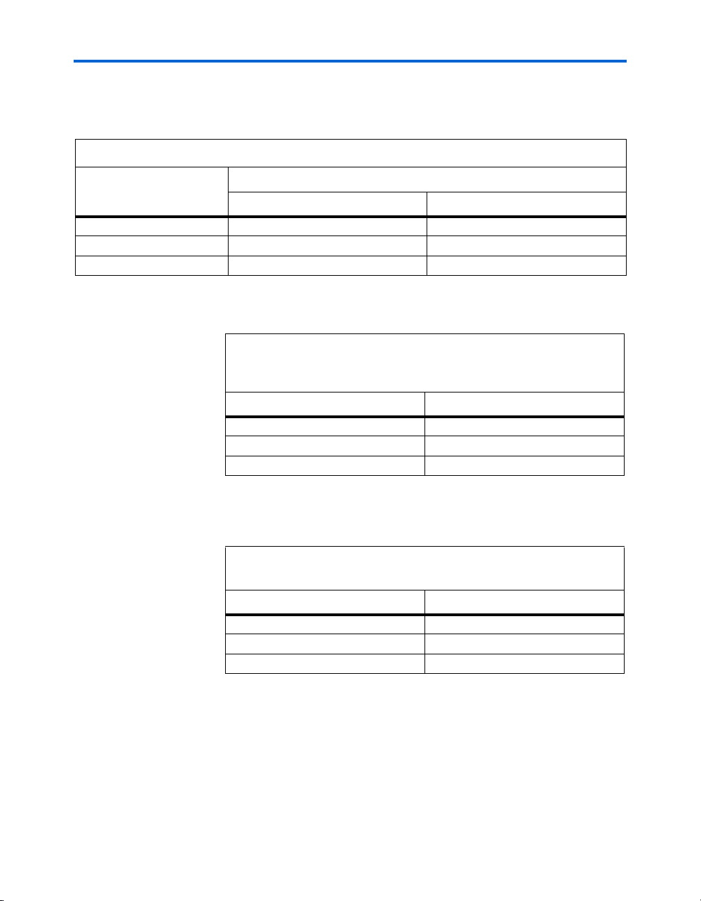
Table 1–1 provides information about this release of the Altera® QDRII
SRAM Controller MegaCore® function.
Table 1–1. Release Information
Item Description
Ver si on 9. 1
Release Date November 2009
Ordering Code IP-SRAM/QDRII
Product ID 00A4
Vendor ID 6AF7
Release Notes and Errata.
Altera verifies that the current version of the Quartus® II software
compiles the previous version of each MegaCore function. The MegaCore
IP Library Release Notes and Errata report any exceptions to this
verification. Altera does not verify compilation with MegaCore function
versions older than one release.
MegaCore functions provide either full or preliminary support for target
Altera device families:
■ Full support means the MegaCore function meets all functional and
timing requirements for the device family and may be used in
production designs
■ Preliminary support means the MegaCore function meets all
functional requirements, but may still be undergoing timing analysis
for the device family; it may be used in production designs with
caution.
Altera Corporation MegaCore Version 9.1 1–1
November 2009
Page 6

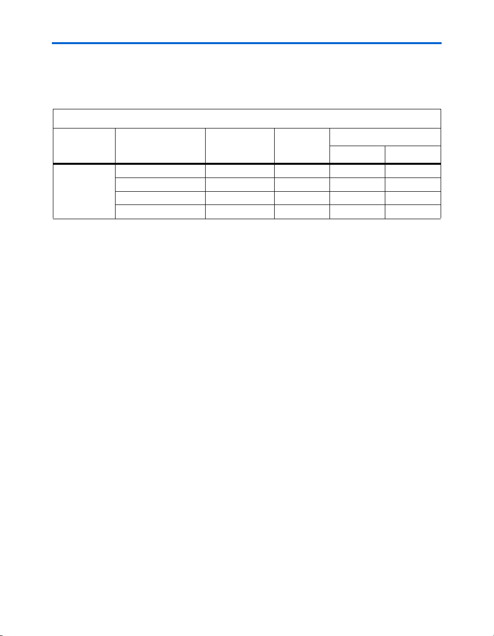
Features
Table 1–2 shows the level of support offered by the QDRII SRAM
Controller MegaCore function to each Altera device family.
Table 1–2. Device Family Support
Device Family Support
HardCopy® II
®
Stratix
Stratix
II Full
Stratix
II GX
Stratix GX Full
Other device families (1) No support
Note to Ta b l e 1– 2 :
(1) For more information on support for Stratix III or Stratix IV devices, contact
Altera.
Preliminary
Full
Full
Features
General Description
■ Support for burst of two and four memory type
■ Support for 8-, 18-, and 36-bit QDRII interfaces
■ Support for two-times and four-times data width on the local side
(four-times for burst of four only)
■ Operates at 300 MHz for QDRII and QDRII+ SRAM
■ Automatic concatenation of consecutive reads and writes (narrow
local bus width mode only)
■ Easy-to-use IP Toolbench interface
■ IP functional simulation models for use in Altera-supported VHDL
and Verilog HDL simulators
■ Support for OpenCore Plus evaluation
The QDRII SRAM Controller MegaCore function provides an easy-to-use
interface to QDRII SRAM modules. The QDRII SRAM Controller ensures
that the placement and timing are in line with QDRII specifications.
The QDRII SRAM Controller is optimized for Altera Stratix series. The
advanced features available in these devices allow you to interface
directly to QDRII SRAM devices.
Figure 1–1 shows a system-level diagram including the example design
that the QDRII SRAM Controller MegaCore function creates for you.
1–2 MegaCore Version 9.1 Altera Corporation
QDRII SRAM Controller MegaCore Function User Guide November 2009
Page 7
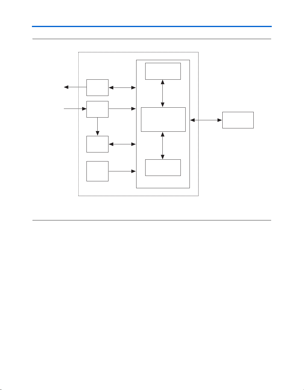
Figure 1–1. QDRII SRAM Controller System-Level Diagram
Example Design
Control Logic
(Encrypted)
Pass
or Fail
Example
Driver
Local
Interface
About This MegaCore Function
Clock
Notes to Figure 1–1:
(1) Optional, for Stratix II devices only.
(2) Non-DQS mode only.
System
PLL
DLL (1)
Fedback
Clock
PLL (
2
)
The IP Toolbench-generated example design instantiates a phase-locked
loop (PLL), an optional DLL (for Stratix II devices only), an example
driver, and your QDRII SRAM Controller custom variation. The example
design is a fully-functional example design that can be simulated,
synthesized, and used in hardware. The example driver is a self-test
module that issues read and write commands to the controller and checks
the read data to produce the pass/fail and test complete signals.
Resynchronization
& Pipeline Logic
(Clear Text)
Datapath
(Clear Text)
QDRII SRAM Controller
QDRII
SRAM
Interface
QDRII SRAM
You can replace the QDRII SRAM controller encrypted control logic in
the example design with your own custom logic, which allows you to use
the Altera clear-text resynchronization and pipeline logic and datapath
with your own control logic.
OpenCore Plus Evaluation
With Altera’s free OpenCore Plus evaluation feature, you can perform
the following actions:
Altera Corporation MegaCore Version 9.1 1–3
November 2009 QDRII SRAM Controller MegaCore Function User Guide
Page 8
Performance and Resource Utilization
■ Simulate the behavior of a megafunction (Altera MegaCore function
or AMPPSM megafunction) within your system
■ Verify the functionality of your design, as well as evaluate its size
and speed quickly and easily
■ Generate time-limited device programming files for designs that
include megafunctions
■ Program a device and verify your design in hardware
You only need to purchase a license for the megafunction when you are
completely satisfied with its functionality and performance, and want to
take your design to production.
f For more information on OpenCore Plus hardware evaluation using the
QDRII SRAM Controller, refer to “OpenCore Plus Time-Out Behavior”
on page 3–10 and AN 320: OpenCore Plus Evaluation of Megafunctions.
Performance
and Resource
Utilization
Table 1–3 shows typical expected performance for the QDRII SRAM
Controller MegaCore function, with the Quartus II software version 9.1.
1 The example driver, which only demonstrates basic read and
write operation, can limit the performance, particularly in wide
interfaces. To improve performance, replace the example driver
or remove it and use the virtual pins on the controller.
Table 1–3. Performance
(MHz)
Device
Stratix II (EP2S60F1020C3) 300
Stratix II GX (EP2SGX30CF780C3) 300
Stratix (EP1S25F780C5) 200
Stratix II and Stratix II GX devices support QDRII SRAM at up to
300 MHz/1,200 Megabits per second (Mbps). Stratix and Stratix GX
devices support QDRII SRAM at up to 200 MHz/800 Mbps. Tables 1–4
through 1–6 show the clock frequency support for each device family,
with the Quartus II software version 9.1.
f
MAX
1–4 MegaCore Version 9.1 Altera Corporation
QDRII SRAM Controller MegaCore Function User Guide November 2009
Page 9
About This MegaCore Function
1 These numbers apply to both commercial and industrial
devices.
Table 1–4. QDRII SDRAM Maximum Clock Frequency Support in Stratix II & Stratix II GX Devices (1)
Speed Grade
Frequency (MHz)
DLL-Based Implementation PLL-Based Implementation
–3 300 200
–4 200 167
–5 200 167
Notes to Ta b l e 1– 4 :
(1) This analysis is based on the EP2S90F1020 device. Ensure you perform a timing analysis for your chosen FPGA.
Table 1–5. QDRII SRAM Maximum Clock Frequency Supported in Stratix &
Stratix GX Devices (EP1S10 to EP1S40 & EP1SGX10 to EP1SGX40 Devices)
(1)
Speed Grade Frequency (MHz)
–5 200
–6 167
–7 133
Notes to Ta b l e 1– 5 :
(1) This analysis is based on the EP1S25F1020 device. Ensure you perform a timing
analysis for your chosen FPGA.
Table 1–6. QDRII SRAM Maximum Clock Frequency Supported in Stratix
Devices (EP1S60 to EP1S80 Devices) (1)
Speed Grade Frequency (MHz)
–5 167
–6 167
–7 133
Notes to Ta b l e 1– 6 :
(1) This analysis is based on the EP1S60F1020 device. Ensure you perform a timing
analysis for your chosen FPGA.
Altera Corporation MegaCore Version 9.1 1–5
November 2009 QDRII SRAM Controller MegaCore Function User Guide
Page 10
Performance and Resource Utilization
Table 1–7 shows typical sizes in combinational adaptive look-up tables
(ALUTs) and logic registers for a QDRII SRAM controller with a burst
length of 4 in narrow mode.
Table 1–7. Typical Size (1)
Device Memory Width (Bits)
Stratix II 9 360 598 – 1
18 369 633 1 –
36 390 708 2 –
72 (2 × 36) 459 880 4 –
Notes to Ta b l e 1– 7 :
(1) These sizes are a guide only and vary with different choices of parameters.
Combinational
ALUTs
Logic
Registers
Memory Blocks
M4K M512
1–6 MegaCore Version 9.1 Altera Corporation
QDRII SRAM Controller MegaCore Function User Guide November 2009
Page 11
2. Getting Started
Design Flow
To evaluate the QDRII SRAM Controller using the OpenCore Plus
feature, include these steps in your design flow:
1. Obtain and install the QDRII SRAM Controller.
The QDRII SRAM Controller is part of the MegaCore IP Library, which is
distributed with the Quartus II software and downloadable from the
Altera website, www.altera.com.
f For system requirements and installation instructions, refer to Altera
Software Installation and Licensing.
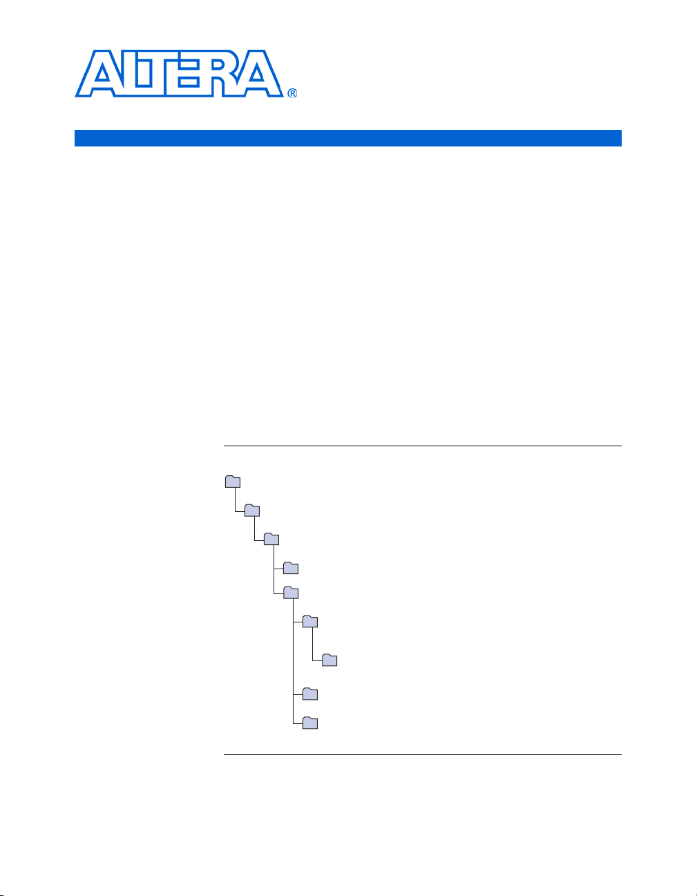
Figure 2–1 shows the directory structure after you install the QDRII
SRAM Controller, where <path> is the installation directory. The default
installation directory on Windows is c:\altera\<version>; on Linux it is
/opt/altera<version>.
Figure 2–1. Directory Structure
<path>
Installation directory.
ip
Contains the Altera MegaCore IP Library and third-party IP cores.
altera
Contains the Altera MegaCore IP Library.
common
Contains shared components.
qdrii_sram_controller
Contains the QDRII SRAM Controller MegaCore function files and documentation.
constraints
Contains scripts that generate an instance-specific Tcl script for each instance of
the QDRII SRAM Controller in various Altera devices.
dat
Contains a data file for each Altera device combination that is used by the
Tcl script to generate the instance-specific Tcl script.
doc
Contains the documentation for the QDRII SRAM Controller MegaCore function.
lib
Contains encrypted lower-level design files and other support files.
2. Create a custom variation of the QDRII SRAM Controller MegaCore
function using IP Toolbench.
Altera Corporation MegaCore Version 9.1 2–1
November 2009
Page 12

QDRII SRAM Controller Walkthrough
1 IP Toolbench is a toolbar from which you quickly and easily
3. Implement the rest of your design using the design entry method of
your choice.
4. Use the IP Toolbench-generated IP functional simulation model to
verify the operation of your design.
f For more information on IP functional simulation models, refer to the
Simulating Altera IP in Third-Party Simulation Tools chapter in volume 3 of
the Quartus II Handbook.
5. Edit the PLL(s).
6. Use the Quartus II software to add constraints to the example
design and compile the example design.
7. Perform gate-level timing simulation, or if you have a suitable
development board, you can generate an OpenCore Plus
time-limited programming file, which you can use to verify the
operation of the example design in hardware.
view documentation, specify parameters, and generate all
of the files necessary for integrating the parameterized
MegaCore function into your design.
8. Either obtain a license for the QDRII SRAM controller MegaCore
function or replace the encrypted QDRII SRAM controller control
logic with your own logic and use the clear-text data path.
1 If you obtain a license for the QDRII SRAM controller, you
must set up licensing.
9. Generate a programming file for the Altera device(s) on your board.
10. Program the Altera device(s) with the completed design.
QDRII SRAM
Controller
Walkthrough
2–2 MegaCore Version 9.1 Altera Corporation
QDRII SRAM Controller MegaCore Function User Guide November 2009
This walkthrough explains how to create a QDRII SRAM controller using
the Altera QDRII SRAM controller IP Toolbench and the Quartus II
software. When you are finished generating a custom variation of the
QDRII SRAM Controller MegaCore function, you can incorporate it into
your overall project.
1 IP Toolbench only allows you to select legal combinations of
parameters, and warns you of any invalid configurations.
This walkthrough requires the following steps:
Page 13

Getting Started
■ “Create a New Quartus II Project” on page 2–3
■ “Launch IP Toolbench” on page 2–4
■ “Step 1: Parameterize” on page 2–5
■ “Step 2: Constraints” on page 2–7
■ “Step 3: Set Up Simulation” on page 2–7
■ “Step 4: Generate” on page 2–8
Create a New Quartus II Project
Before you begin, you must create a new Quartus II project. With the New
Project wizard, you specify the working directory for the project, assign
the project name, and designate the name of the top-level design entity.
You will also specify the QDRII SRAM Controller user library. To create a
new project, follow these steps:
You need to create a new Quartus II project with the New Project Wizard,
which specifies the working directory for the project, assigns the project
name, and designates the name of the top-level design entity. To create a
new project follow these steps:
1. Choose Programs > Altera > Quartus II <version> (Windows Start
menu) to run the Quartus II software. Alternatively, you can use the
Quartus II Web Edition software.
2. Choose New Project Wizard (File menu).
3. Click Next in the New Project Wizard Introduction page (the
introduction page does not display if you turned it off previously).
4. In the New Project Wizard: Directory, Name, Top-Level Entity
page, enter the following information:
a. Specify the working directory for your project. For example,
this walkthrough uses the c:\altera\temp\qdr_project
directory.
b. Specify the name of the project. This walkthrough uses project
for the project name.
1 The Quartus II software automatically specifies a top-level
design entity that has the same name as the project. Do not
change it.
5. Click Next to close this page and display the New Project Wizard:
Add Files page.
Altera Corporation MegaCore Version 9.1 2–3
November 2009 QDRII SRAM Controller MegaCore Function User Guide
Page 14

QDRII SRAM Controller Walkthrough
1 When you specify a directory that does not already exist, a
6. If you installed the MegaCore IP Library in a different directory
from where you installed the Quartus II software, you must add the
user libraries:
a. Click User Libraries.
b. Type <path>\ip into the Library name box, where <path> is the
c. Click Add to add the path to the Quartus II project.
d. Click OK to save the library path in the project.
7. Click Next to close this page and display the New Project Wizard:
Family & Device Settings page.
8. On the New Project Wizard: Family & Device Settings page,
choose the target device family in the Family list.
9. The remaining pages in the New Project Wizard are optional. Click
Finish to complete the Quartus II project.
message asks if the specified directory should be created.
Click Yes to create the directory.
directory in which you installed the QDRII SRAM Controller.
You have finished creating your new Quartus II project.
Launch IP Toolbench
To launch IP Toolbench in the Quartus II software, follow these steps:
1. Start the MegaWizard® Plug-In Manager by choosing MegaWizard
Plug-In Manager (Tools menu). The MegaWizard Plug-In Manager
dialog box displays.
1 Refer to Quartus II Help for more information on how to
use the MegaWizard Plug-In Manager.
2. Specify that you want to create a new custom megafunction
variation and click Next.
3. Expand the Interfaces > Memory Controllers directory then click
QDRII SRAM Controller-v8.1.
4. Select the output file type for your design; the wizard supports
VHDL and Verilog HDL.
2–4 MegaCore Version 9.1 Altera Corporation
QDRII SRAM Controller MegaCore Function User Guide November 2009
Page 15

Getting Started
5. The MegaWizard Plug-In Manager shows the project path that you
specified in the New Project Wizard. Append a variation name for
the MegaCore function output files <project path>\<variation name>.
1 The <variation name> must be a different name from the
project name and the top-level design entity name.
6. Click Next to launch IP Toolbench.
Step 1: Parameterize
To parameterize your MegaCore function, follow these steps:
1. Click Step 1: Parameterize in IP Toolbench.
f For more information on the parameters, refer to “Parameters” on
page 3–29).
2. Set the memory type:
a. Choose the Memory device.
b. Select either QDRII or QDRII+.
c. Set the Clock speed.
d. Choose the Voltage.
e. Choose the Burst length.
f. Choose the Data bus width.
g. Choose the Address bus width.
h. Choose the Memory Latency.
i. Select the Narrow mode or Wide mode to set the local bus
width.
3. Set the memory interface.
a. Set Device width.
b. Set Device depth.
c. Turn off Use ALTDDIO pin, if you are targeting HardCopy II
devices.
Altera Corporation MegaCore Version 9.1 2–5
November 2009 QDRII SRAM Controller MegaCore Function User Guide
Page 16

QDRII SRAM Controller Walkthrough
4. Click Board & Controller tab or Next.
f For more information on board and controller parameters, refer to
“Board & Controller” on page 3–31.
5. Choose the number of pipeline registers.
6. To set the read latency, turn on Manual read latency setting and
specify the latency at Set latency to clock cycle.
7. Turn on the appropriate capture mode—DQS or non-DQS capture
mode. If you turn off Enable DQS mode (non-DQS capture mode),
you can turn on Use migratable bytegroups.
8. Enter the pin loading for the FPGA pins.
9. Click Project Settings tab or Next.
f For more information on the project settings, refer to “Project Settings”
on page 3–33.
10. Altera recommends that you turn on Automatically apply QDRII
SRAM controller-specific constraints to the Quartus II project so
that the Quartus II software automatically applies the constraints
script when you compile the example design.
11. En sure Update the example design that instantiates the QDRII
SRAM controller variation is turned on, for IP Toolbench to
automatically update the example design file.
12. Turn off Update example design system PLL, if you have edited the
PLL and you do not want the wizard to regenerate the PLL when
you regenerate the variation.
1 The first time you create a custom variation, you must turn
on Update example design system PLL.
13. The constraints script automatically detects the hierarchy of your
design. The constraints script analyzes and elaborates your design
to automatically extract the hierarchy to your variation. To prevent
the constraints script analyzing and elaborating your design, turn
on Enable hierarchy control, and enter the correct hierarchy path to
your variation. The hierarchy path is the path to your QDRII SRAM
controller, without the top-level name. Figure 2–2 shows the
following example hierarchy:
my_system:my_system_inst|sub_system:sub_system_inst|
2–6 MegaCore Version 9.1 Altera Corporation
QDRII SRAM Controller MegaCore Function User Guide November 2009
Page 17
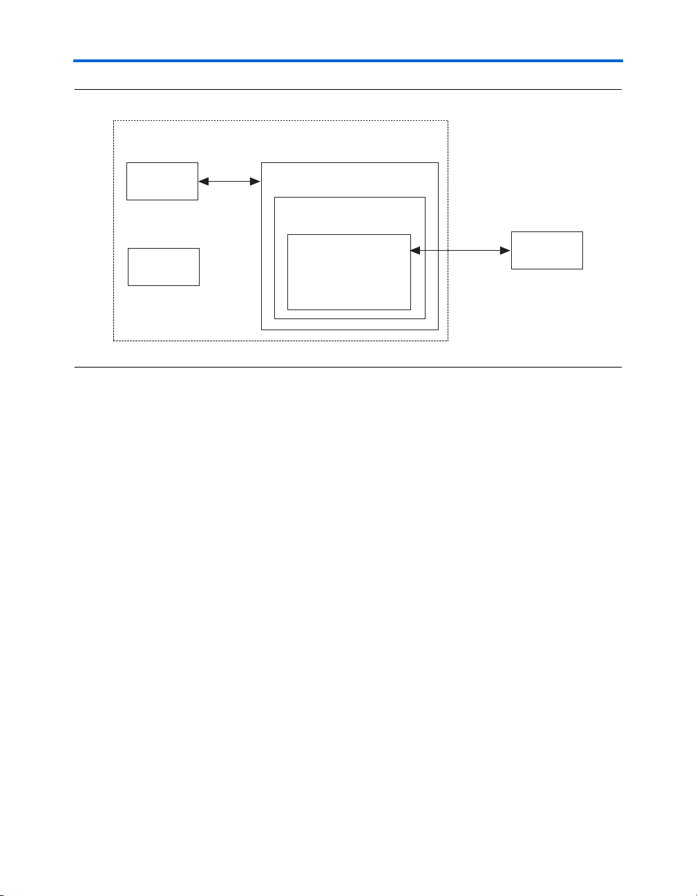
Figure 2–2. System Naming
QDRII SRAM
Other Logic
PLL
QDRII SRAM
Interface
example_top
Example Design
QDRII SRAM Controller
my_system_inst
System
sub_system_inst
Subsystem
Getting Started
14. IP Toolbench uses a prefix (e.g., qdrii_) for the names of all memory
interface pins. Enter a prefix for all memory interface pins
associated with this custom variation.
15. Click Finish.
Step 2: Constraints
To choose the constraints for your device, follow these steps:
1. Click Step 2: Constraints in IP Toolbench.
2. Choose the positions on the device for each of the QDRII SRAM
byte groups. To place a byte group, select the byte group in the
drop-down box at your chosen position.
1 The floorplan matches the orientation of the Quartus II
floorplanner. The layout represents the die as viewed from
Step 3: Set Up Simulation
An IP functional simulation model is a cycle-accurate VHDL or Verilog
HDL model produced by the Quartus II software. The model allows for
fast functional simulation of IP using industry-standard VHDL and
Verilog HDL simulators.
Altera Corporation MegaCore Version 9.1 2–7
November 2009 QDRII SRAM Controller MegaCore Function User Guide
above. A byte group consists of a cq pin and a number of q
pins (the same number as the data width).
Page 18

QDRII SRAM Controller Walkthrough
c You may only use these simulation model output files for
To generate an IP functional simulation model for your MegaCore
function, follow these steps:
1. Click Step 3: Set Up Simulation in IP Toolbench.
2. Turn on Generate Simulation Model.
3. Choose the language in the Language list.
4. Some third-party synthesis tools can use a netlist that contains only
the structure of the MegaCore function, but not detailed logic, to
optimize performance of the design that contains the MegaCore
function. If your synthesis tool supports this feature, turn on
Generate netlist.
5. Click OK.
Step 4: Generate
simulation purposes and expressly not for synthesis or any
other purposes. Using these models for synthesis will create a
nonfunctional design.
1. To generate your MegaCore function, click Step 4: Generate in IP
To ol be n ch .
1 The Quartus II IP File (.qip) is a file generated by the
MegaWizard interface, and contains information about a
generated IP core. You are prompted to add this .qip file to the
current Quartus II project at the time of file generation. In most
cases, the .qip file contains all of the necessary assignments and
information required to process the core or system in the
Quartus II compiler. Generally, a single .qip file is generated for
each MegaCore function or system in the Quartus II compiler.
2–8 MegaCore Version 9.1 Altera Corporation
QDRII SRAM Controller MegaCore Function User Guide November 2009
Page 19

Getting Started
Table 2–1 describes the generated files and other files that may be in your
project directory. The names and types of files specified in the IP
Toolbench report vary based on whether you created your design with
VHDL or Verilog HDL
Table 2–1. Generated Files (Part 1 of 2) (1), (2) & (3)
Filename Description
<variation name>.bsf Quartus II symbol file for the MegaCore function
variation. You can use this file in the Quartus II block
diagram editor.
<variation name>.html MegaCore function report file.
<variation name>.vhd, or .v A MegaCore function variation file, which defines a
VHDL or Verilog HDL top-level description of the custom
MegaCore function. Instantiate the entity defined by this
file inside of your design. Include this file when compiling
your design in the Quartus II software.
<variation name>_bb.v Verilog HDL black-box file for the MegaCore function
variation. Use this file when using a third-party EDA tool
to synthesize your design.
<variation name>_auk_qdrii_sram.vhd or .v File that instantiates the control logic and the datapath.
<variation
name>_auk_qdrii_sram_addr_cmd_reg.vhd or .v
<variation
name>_auk_qdrii_sram_avalon_controller_ipfs_
wrap.vhd or .v
<variation
name>_auk_qdrii_sram_avalon_controller_ipfs_
wrap.vho or .vo
<variation
name>_auk_qdrii_sram_capture_group_wrapper.
vhd or .v
<variation name>_auk_qdrii_sram_clk_gen.vhd or .vThe clock output generators.
The address and command output registers.
File that instantiates the controller.
VHDL or Verilog HDL IP functional simulation model.
File that contains all the capture group modules (CQ and
CQN group modules and read capture registers).
<variation
name>_auk_qdrii_sram_cq_cqn_group.vhd or .v
<variation name>_auk_qdrii_sram_datapath.vhd
or .v
<variation name>_auk_qdrii_sram_dll.vhd or .v DLL.
<variation
name>_auk_qdrii_sram_example_driver
.vhd or .v
<variation
name>_auk_qdrii_sram_read_group.vhd or .v
Altera Corporation MegaCore Version 9.1 2–9
November 2009 QDRII SRAM Controller MegaCore Function User Guide
The CQ and CQN module.
Datapath.
The example driver.
The read capture registers.
Page 20

QDRII SRAM Controller Walkthrough
Table 2–1. Generated Files (Part 2 of 2) (1), (2) & (3)
Filename Description
<variation
name>_auk_qdrii_sram_pipe_resynch_wrapper.v
hd or .v
<variation
name>_auk_qdrii_sram_pipeline_addr_cmd.vhd
or .v
<variation
name>_auk_qdrii_sram_pipeline_rdata.vhd or .v
<variation
name>_auk_qdrii_sram_pipeline_wdata.vhd or .v
<variation
name>_auk_qdrii_sram_read_group.vhd or .v
<variation
name>_auk_qdrii_sram_resynch_reg.vhd or .v
<variation
name>_auk_qdrii_sram_train_wrapper.vhd or .v
<variation
name>_auk_qdrii_sram_test_group.vhd or .v
<variation
name>_auk_qdrii_sram_write_group.vhd or .v
<variation name>.qip Contains Quartus II project information for your
<top-level name>.vhd or .v (1) Example design file.
add_constraints_for_
qdrii_pll_stratixii.vhd or .v Stratix II PLL.
<variation name>.tcl The add constraints script.
File that includes the write data pipeline and includes the
address and command, read command, write data, and
write command pipeline.
Address and command pipeline.
Read data pipeline.
Write data pipeline.
The read registers.
The resynchronization FIFO buffers.
File that contains all the training group modules.
Training module, which realigns latency.
The write registers.
MegaCore function variations.
Notes to Ta b l e 2– 1 :
(1) <top-level name> is the name of the Quartus II project top-level entity.
(2) <variation name> is the name you give to the controller you create with the Megawizard.
(3) IP Tooblench replaces the string qdrii_sram with qdriiplus_sram for QDRII+ SRAM controllers.
2. After you review the generation report, click Exit to close IP
To ol be n ch .
You have finished the walkthrough. Now, simulate the example design
(refer to “Simulate the Example Design” on page 2–11), edit the PLL(s)
(refer to “Edit the PLL” on page 2–18), and compile (refer to “Compile the
Example Design” on page 2–19).
2–10 MegaCore Version 9.1 Altera Corporation
QDRII SRAM Controller MegaCore Function User Guide November 2009
Page 21

Getting Started
Simulate the Example Design
f For more information on the testbench, refer to “Example Design” on
This section describes the following simulation techniques:
■ Simulate with IP Functional Simulation Models
■ Simulating With the ModelSim Simulator
■ Simulating With Other Simulators
■ Simulating in Third-Party Simulation Tools Using NativeLink
Simulate with IP Functional Simulation Models
You can simulate the example design using the IP Toolbench-generated IP
functional simulation models. IP Toolbench generates a VHDL or Verilog
HDL testbench for your example design, which is in the testbench
directory in your project directory.
page 3–27.
You can use the IP functional simulation model with any
Altera-supported VHDL or Verilog HDL simulator. The instructions for
the ModelSim simulator are different to other simulators.
Simulating With the ModelSim Simulator
Altera supplies a generic memory model, lib\qdrii_model.v, which
allows you to simulate the example design with the ModelSim simulator.
To simulate the example design with the ModelSim® simulator, follow
these steps:
1. Copy the generic memory model to the <directory name>\testbench
directory.
2. Open the memory model and the testbench (<top-level
name>_vsim.v or .vhd) in a text editor and ensure the signal names
have the same capitalization in both files.
3. Start the ModelSim-Altera simulator.
4. Change your working directory to your IP Toolbench-generated file
directory <directory name>\testbench\modelsim.
5. To simulate with an IP functional simulation model simulation, type
the following command:
source <variation name>_vsim.tcl
Altera Corporation MegaCore Version 9.1 2–11
November 2009 QDRII SRAM Controller MegaCore Function User Guide
r
Page 22

Simulate the Example Design
6. For a gate-level timing simulation (VHDL or Verilog HDL
ModelSim output from the Quartus II software), type the following
commands:
set use_gate_model 1
r
source <variation name>_vsim.tclr
Simulating With Other Simulators
The IP Toollbench-generated Tcl script is for the ModelSim simulator
only. If you prefer to use a different simulation tool, follow these
instructions. You can also use the generated script as a guide. You also
need to download and compile an appropriate memory model.
1 The following variables apply in this section:
● <QUARTUS ROOTDIR> is the Quartus II installation directory
● <simulator name> is the name of your simulation tool
● <device name> is the Altera device family name
● <project name> is the name of your Quartus II top-level entity or
module.
● <MegaCore install directory> is the QDRII SRAM Controller
installation directory
VHDL IP Functional Simulations
For VHDL simulations with IP functional simulation models, follow
these steps:
1. Create a directory in the <project directory>\testbench directory.
2. Launch your simulation tool inside this directory and create the
following libraries:
● altera_mf
● lpm
● sgate
● <device name>
● auk_qdrii_lib
2–12 MegaCore Version 9.1 Altera Corporation
QDRII SRAM Controller MegaCore Function User Guide November 2009
Page 23

3. Compile the files in Table 2–2 into the appropriate library. The files
are in VHDL93 format.
Table 2–2. Files to Compile—VHDL IP Functional Simulation Models
Library Filename
altera_mf <QUARTUS ROOTDIR>/eda/sim_lib/altera_mf_components.vhd
<QUARTUS ROOTDIR>/eda/sim_lib/altera_mf.vhd
lpm <QUARTUS ROOTDIR>/eda/sim_lib/220pack.vhd
<QUARTUS ROOTDIR>/eda/sim_lib/220model.vhd
sgate <QUARTUS ROOTDIR>/eda/sim_lib/sgate_pack.vhd
<QUARTUS ROOTDIR>/eda/sim_lib/sgate.vhd
<device name><QUARTUS ROOTDIR>/eda/sim_lib/<device name>_atoms.vhd
<QUARTUS ROOTDIR>/eda/sim_lib/<device name>_components.vhd
auk_qdrii_lib <project directory>/<variation name>_auk_qdrii_sram_clk_gen.vhd
<project directory>/<variation name>_auk_qdrii_sram_addr_cmd_reg.vhd
<project directory>/<variation name>_auk_qdrii_sram_cq_cqn_group.vhd
<project directory>/<variation name>_auk_qdrii_sram_read_group.vhd
<project directory>/<variation name>_auk_qdrii_sram_capture_group_wrapper.vhd
<project directory>/<variation name>_auk_qdrii_sram_resynch_reg.vhd
<project directory>/<variation name>_auk_qdrii_sram_write_group.vhd
project directory>/<variation name>_auk_qdrii_sram_datapath.vhd
<
<project directory>/<variation name>_auk_qdrii_sram_test_group.vhd
<project directory>/<variation name>_auk_qdrii_sram_train_wrapper.vhd
<project directory>/<variation name>_auk_qdrii_sram_pipeline_wdata.vhd
<project directory>/<variation name>_auk_qdrii_sram_pipeline_rdata.vhd
<project directory>/<variation name>_auk_qdrii_sram_pipeline_addr_cmd.vhd
<project directory>/<variation name>_auk_qdrii_sram_pipe_resynch_wrapper.vhd
<project directory>/<variation
name>_auk_qdrii_sram_avalon_controller_ipfs_wrap.vho
<project directory>/<variation name>_auk_qdrii_sram.vhd
<project directory>/<variation name>.vhd
<project directory>/qdrii_pll_stratixii.vhd
<project directory>/<variation name>_auk_qdrii_sram_dll.vhd
<project directory>/<variation name>_auk_qdrii_sram_example_driver.vhd
<project directory>/<project name>.vhd
<project directory>/testbench/<project name>_tb.vhd
Getting Started
Altera Corporation MegaCore Version 9.1 2–13
November 2009 QDRII SRAM Controller MegaCore Function User Guide
Page 24

Simulate the Example Design
4. Set the Tcl variable gRTL_DELAYS to 1, which tells the testbench to
model the extra delays in the system necessary for RTL simulation
5. Load the testbench in your simulator with the timestep set to
picoseconds.
VHDL Gate-Level Simulations
For VHDL simulations with gate-level models, follow these steps:
1. Create a directory in the <project directory>\testbench directory.
2. Launch your simulation tool inside this directory and create the
following libraries.
● <device name>
● auk_qdrii_lib
3. Compile the files in Table 2–3 into the appropriate library. The files
are in VHDL93 format.
Table 2–3. Files to Compile—VHDL Gate-Level Simulations
Library Filename
<device name><QUARTUS ROOTDIR>/eda/sim_lib/<device name>_atoms.vhd
<QUARTUS ROOTDIR>/eda/sim_lib/<device name>_components.vhd
auk_qdrii_lib <project directory>/simulation/<simulator name>/<project name>.vho
<project directory>/testbench/<project name>_tb.vhd
4. Set the Tcl variable gRTL_DELAYS to 0, which tells the testbench not
to use the insert extra delays in the system, because these are
applied inside the gate-level model.
5. Load the testbench in your simulator with the timestep set to
picoseconds.
Verilog HDL IP Functional Simulations
For Verilog HDL simulations with IP functional simulation models,
follow these steps:
1. Create a directory in the <project directory>\testbench directory.
2. Launch your simulation tool inside this directory and create the
following libraries.:
2–14 MegaCore Version 9.1 Altera Corporation
QDRII SRAM Controller MegaCore Function User Guide November 2009
Page 25

● altera_mf_ver
● lpm_ver
● sgate_ver
● <device name>_ver
● auk_qdrii_lib
3. Compile the files in Table 2–4 into the appropriate library.
Table 2–4. Files to Compile—Verilog HDL IP Functional Simulation Models (Part 1 of 2)
Library Filename
altera_mf_ver <QUARTUS ROOTDIR>/eda/sim_lib/altera_mf.v
lpm_ver <QUARTUS ROOTDIR>/eda/sim_lib/220model.v
sgate_ver <QUARTUS ROOTDIR>/eda/sim_lib/sgate.v
<device name>_ver <QUARTUS ROOTDIR>/eda/sim_lib/<device name>_atoms.v
Getting Started
Altera Corporation MegaCore Version 9.1 2–15
November 2009 QDRII SRAM Controller MegaCore Function User Guide
Page 26

Simulate the Example Design
Table 2–4. Files to Compile—Verilog HDL IP Functional Simulation Models (Part 2 of 2)
Library Filename
auk_qdrii_lib <project directory>/<variation name>_auk_qdrii_sram_clk_gen.v
<project directory>/<variation name>_auk_qdrii_sram_addr_cmd_reg.v
<project directory>/<variation name>_auk_qdrii_sram_cq_cqn_group.v
<project directory>/<variation name>_auk_qdrii_sram_read_group.v
<project directory>/<variation
name>_auk_qdrii_sram_capture_group_wrapper.v
<project directory>/<variation name>_auk_qdrii_sram_resynch_reg.v
<project directory>/<variation name>_auk_qdrii_sram_write_group.v
<project directory>/<variation name>_auk_qdrii_sram_datapath.v
<project directory>/<variation name>_auk_qdrii_sram_test_group.v
<project directory>/<variation name>_auk_qdrii_sram_train_wrapper.v
<project directory>/<variation name>_auk_qdrii_sram_pipeline_wdata.v
<project directory>/<variation name>_auk_qdrii_sram_pipeline_rdata.v
<project directory>/<variation
name>_auk_qdrii_sram_pipeline_addr_cmd.v
<project directory>/<variation
name>_auk_qdrii_sram_pipe_resynch_wrapper.v
<project directory>/<variation
name>_auk_qdrii_sram_avalon_controller_ipfs_wrap.vo
<project directory>/<variation name>_auk_qdrii_sram.v
<project directory>/<variation name>.v
<project directory>/qdrii_pll_stratixii.v
<project directory>/<variation name>_auk_qdrii_sram_dll.v
<project directory>/<variation name>_auk_qdrii_sram_example_driver.v
<project directory>/<project name>.v
<project directory>/testbench/<project name>_tb.vhd
4. Set the Tcl variable gRTL_DELAYS to 1, which tells the testbench to
model the extra delays in the system necessary for RTL simulation.
5. Configure your simulator to use transport delays, a timestep of
picoseconds and to include the auk_qdrii_lib, sgate_ver, lpm_ver,
altera_mf_ver, and <device name>_ver libraries.
Verilog HDL Gate-Level Simulations
For Verilog HDL simulations with gate-level models, follow these steps:
2–16 MegaCore Version 9.1 Altera Corporation
QDRII SRAM Controller MegaCore Function User Guide November 2009
Page 27

Getting Started
1. Create a directory in the <project directory>\testbench directory.
2. Launch your simulation tool inside this directory and create the
following libraries:
● <device name>_ver
● auk_qdrii_lib
3. Copy the <project directory>/simulation/<simulator name>_v.sdo file
into the compilation directory.
4. Compile the files in Table 2–5 into the appropriate library.
Table 2–5. Files to Compile—Verilog HDL Gate-Level Simulations
Library Filename
<device name>_ver <QUARTUS ROOTDIR>/eda/sim_lib/<device name>_atoms.v
auk_qdrii_lib <project directory>/simulation/<simulator name>/<toplevel_name>.vo
<project directory>/testbench/<project name>_tb.v
5. Set the Tcl variable gRTL_DELAYS to 0, which tells the testbench not
to use the insert extra delays in the system, because these are
applied inside the gate level model. Configure your simulator to use
transport delays, a timestep of picoseconds, and to include the
auk_qdrii_lib and <device name>_ver library.
Simulating in Third-Party Simulation Tools Using NativeLink
You can perform a simulation in a third-party simulation tool from within
the Quartus II software, using NativeLink.
f For more information on NativeLink, refer to the Simulating Altera IP
Using NativeLink chapter in volume 3 of the Quartus II Handbook.
To set up simulation in the Quartus II software using NativeLink, follow
these steps:
1. Create a custom variation with an IP functional simulation model.
2. Obtain and copy a memory model to a suitable location, for
example, the testbench directory.
1 Before running the simulation you may also need to edit the
testbench to match the chosen memory model.
Altera Corporation MegaCore Version 9.1 2–17
November 2009 QDRII SRAM Controller MegaCore Function User Guide
Page 28

Edit the PLL
3. Check that the absolute path to your third-party simulator
executable is set. On the Tools menu click Options and select EDA
Tools Options.
4. On the Processing menu, point to Start and click Start Analysis &
Elaboration.
5. On the Assignments menu click Settings, expand EDA Tool
Settings and select Simulation. Select a simulator under Too l N ame
and in NativeLink Settings, select Compile Test Bench and click
Test Benches.
6. Click New.
7. Enter a name for the Test bench name.
8. Enter the name of the automatically generated testbench, <project
name>_tb, in Test bench entity.
9. Enter the name of the top-level instance in Instance.
10. Change Run for to 500 s.
11. Add the testbench files. In the File name field browse to the location
of the memory model and the testbench, <project name>_tb, click OK
and click Add.
12. Click OK.
13. Click OK.
14. On the Tools menu point to EDA Simulation Tool and click Run
EDA RTL Simulation.
Edit the PLL
The IP Toolbench-generated example design includes up to two PLLs
(system PLL and fedback clock PLL), which have an input to output clock
ratio of 1:1 and a clock frequency that you entered in IP Toolbench. In
addition, IP Toolbench correctly sets all the phase offsets of all the
relevant clock outputs for your design. You can edit either PLLs’ input
clock to make it conform to your system requirements. If you re-run IP
Toolbench, it does not overwrite the system PLL, if you turn off Reset the
PLL to the default setting, so your edits are not lost.
f For more information on the PLL, refer to “PLL Configuration” on
page 3–26.
2–18 MegaCore Version 9.1 Altera Corporation
QDRII SRAM Controller MegaCore Function User Guide November 2009
Page 29

Getting Started
To edit the example PLL, follow these steps:
1. Choose MegaWizard Plug-In Manager (Tools menu).
2. Select Edit an existing custom megafunction variation and click
Next.
3. In your Quartus II project directory, for VHDL choose
qdrii_pll_<device name>.vhd; for Verilog HDL choose
qdrii_pll_<device name>.v.
4. Click Next.
5. Edit the PLL parameters in the altpll MegaWizard Plug-In.
f For more information on the altpll megafunction, refer to the
Quartus II Help or click Documentation in the altpll MegaWizard
Plug-In.
Compile the Example Design
Before the Quartus II software compiles the example design it runs the IP
Toolbench-generated Tcl constraints script, auto_add_constraints.tcl.
The auto_add_qdrii_constraints.tcl script calls the
add_constraints_for_<variation name>.tcl script for each variation in your
design. The add_constraints_for_<variation name>.tcl script checks for
any previously added constraints, removes them, and then adds
constraints for that variation.
The constraints script analyzes and elaborates your design, to
automatically extract the hierarchy to your variation. To prevent the
constraints script analyzing and elaborating your design, turn on Enable
hierarchy control in the wizard, and enter the correct hierarchy path to
your data path (refer to step 13 on page 2–6).
When the constraints script runs, it creates another script,
remove_constraints_for_<variation name>.tcl, which you can use to
remove the constraints from your design.
To compile the example instance, follow these steps:
1. Optional. Enable TimeQuest Timing Analyzer.
a. On the Assignments menu click Settings, expand Timin g
Analysis Settings, and select Use TimeQuest Timing
Analyzer.
Altera Corporation MegaCore Version 9.1 2–19
November 2009 QDRII SRAM Controller MegaCore Function User Guide
Page 30

Compile the Example Design
b. Use the DDR timing wizard (DTW) to generate the required
QDRII SRAM Synopsys design constraint (SDC) TimeQuest
constraints for the design.
f For more information on the DTW, refer to the DTW User Guide.
2. Choose Start Compilation (Processing menu), which runs the add
constraints scripts, compiles the example design, and performs
timing analysis.
3. View the Classic or TimeQuest Timing Analyzer to verify your
design meets timing.
If your design does not meet timing requirements, add the following lines
to you .qsf file:
set_instance_assignment -name GLOBAL_SIGNAL OFF -to soft_reset_n
set_global_assignment -name OPTIMIZE_FAST_CORNER_TIMING ON
If the compilation does not reach the frequency requirements, follow
these steps:
1. Choose Settings (Assignments menu).
2. Choose Analysis and Synthesis Settings in the category list.
3. Select Speed in Optimization Technique.
4. Click OK.
5. Re-compile the example design by choosing Start Compilation
(Processing menu).
To view the constraints in the Quartus II Assignment Editor, choose
Assignment Editor (Assignments menu).
1 If you have “?” characters in the Quartus II Assignment Editor,
the Quartus II software cannot find the entity to which it is
applying the constraints, probably because of a hierarchy
mismatch. Either edit the constraints script, or enter the correct
hierarchy path in the Hierarchy tab (refer to step 13 on
page 2–6).
f For more information on constraints, refer to “Constraints” on
page 3–29.
2–20 MegaCore Version 9.1 Altera Corporation
QDRII SRAM Controller MegaCore Function User Guide November 2009
Page 31

Getting Started
Program a Device
f For more information on OpenCore Plus hardware evaluation using the
Implement Your Design
Set Up Licensing
After you have compiled the example design, you can perform gate-level
simulation (refer to “Simulate the Example Design” on page 2–11) or
program your targeted Altera device to verify the example design in
hardware.
With Altera's free OpenCore Plus evaluation feature, you can evaluate the
QDRII SRAM Controller MegaCore function before you obtain a license.
OpenCore Plus evaluation allows you to generate an IP functional
simulation model, and produce a time-limited programming file.
QDRII SRAM Controller MegaCore function, refer to “OpenCore Plus
Evaluation” on page 1–3, “OpenCore Plus Time-Out Behavior” on
page 3–10, and AN 320: OpenCore Plus Evaluation of Megafunctions.
To implement your design based on the example design, replace the
example driver in the example design with your own logic.
You need to obtain a license for the MegaCore function only when you are
completely satisfied with its functionality and performance, and want to
take your design to production.
After you obtain a license for QDRII SRAM Controller, you can request a
license file from the Altera web site at www.altera.com/licensing and
install it on your computer. When you request a license file, Altera emails
you a license.dat file. If you do not have Internet access, contact your
local Altera representative.
Altera Corporation MegaCore Version 9.1 2–21
November 2009 QDRII SRAM Controller MegaCore Function User Guide
Page 32

Set Up Licensing
2–22 MegaCore Version 9.1 Altera Corporation
QDRII SRAM Controller MegaCore Function User Guide November 2009
Page 33

3. Functional Description
avl_clk
avl_clk_wr
avl_resetn
dll_delay_ctrl
resynch_clk
avl_addr_wr
avl_byteen_wr
avl_chipselect_wr
avl_data_wr
avl_write
avl_wait_request_wr
avl_addr_rd
avl_byteen_rd
avl_chipselect_rd
avl_read
avl_data_rd
avl_datavalid_rd
avl_wait_request_rd
Control
Logic
(Encrypted)
QDRII SRAM Controller
Datapath
(Clear Text)
Resynchronization
& Pipeline Logic
(Clear Text)
qdrii_a
qdrii_bwsn
qdrii_cq
qdrii_cqn
qdrii_d
qdrii_k
qdrii_kn
qdrii_q
qdrii_rpsn
qdrii_wpns
Block
Figure 3–1 shows a block diagram of the QDR SRAM controller
MegaCore function.
Description
Figure 3–1. QDRII SRAM Controller Block Diagram (1)
Notes to Figure 3–1:
(1) You can edit the qdrii_ prefix.
Altera Corporation MegaCore Version 9.1 3–1
November 2009
The QDRII SRAM Controller comprises the following three parts:
■ The control logic gets read and write requests from the Avalon
interface and turn them into QDRII SRAM read and write requests,
with the correct timing and concatenating consecutive addresses
where applicable.
■ The resynchronization and pipeline logic provides the
resynchronization system, the training block, and the optional
pipeline logic.
■ The datapath contains all the I/O and the clock generation.
®
Page 34

Block Description
Avalon
Slave
Interface
Write
FSM
Avalon
Slave
Interface
Read
FSM
Pause
Control Logic
(Encrypted)
1 You can use the datapath on its own if you want to create you
own resynchronization scheme or want to have an interface
similar to the QDRII SRAM v1.0.0 interface.
Control Logic
Figure 3–2 shows the control logic block diagram.
Figure 3–2. Control Logic Block Diagram
The basic architecture comprises two separate almost independent
channels. The write channel sends data to the memory. The read channel
receives the data. The address port on the QDRII SRAM interface is
shared— a write takes precedence when simultaneous reads and writes
occur. On the Avalon interface, all the signals are independent.
The write channel comprises an Avalon interface and a small pipeline to
perform two-cycle bursts. A finite state machine (FSM) controls the
signaling to the Avalon interface and deals with the data from Avalon
interface. The data and address are then passed to the I/O and sent to the
memory.
Similarly for the read channel, a FSM controls the signaling to the Avalon
interface and deals with the data going to Avalon interface. The read
command is passed to the QDRII SRAM interface and the data is
3–2 MegaCore Version 9.1 Altera Corporation
QDRII SRAM Controller MegaCore Function User Guide November 2009
captured when arriving back. Simultaneous read and write operations
may lead to pauses on the Avalon read interface.
Page 35

Resynchronization & Pipeline Logic
Optional
Address &
Command
Pipeline
Optional
Read Data
Pipeline
Optional
Write Data
Pipeline
From Datapath
Capture
Registers
To Control
Block
Read FSM
From
Control
Logic
From
Control
Logic
Resynchronization
Resynchronization
Training
Group
Module
Training Group
Modules
Training
Group
Module
Resynchronization
& Pipeline Logic
Figure 3–3 shows the resynchronization and pipeline logic block
diagram.
Figure 3–3. Resynchronization & Pipeline Logic Block Diagram
Functional Description
Address & Command Pipeline
The optional address and command pipeline pipelines all commands and
addresses by a predefined number of cycles.
Altera Corporation MegaCore Version 9.1 3–3
November 2009 QDRII SRAM Controller MegaCore Function User Guide
Page 36

Block Description
Write Data Pipeline
The write data pipeline pipelines the write data by a specified number of
clock cycles.The number of pipelines is equal to the address and
command pipelines, because the controller already aligns the data,
address and command correctly, therefore the amount of delay going to
the I/O is identical.
Training Group Module
The training group module sends all the control, data, and address
during training; it reverts to the controller-issued signals after training. It
also pauses the controllers for the duration of the training and sends some
feedback to the resynchronization logic to realign the pointers to get to
the desired latency. To ensure stability the read pointer is aligned only
after the DLL is stable. The write pointer is synchronously reset after the
read pointer. You can view the training signals from outside the example
design.
Read Data Pipeline
The optional read data pipeline pipelines the data after it is
resynchronized by a predefined number of cycles.
Resynchronization Logic
The resynchronization logic transfers the data from the QDRII SRAM
clock domain onto the system clock domain.
A small dual-port RAM block resynchronizes the data onto the system
clock. It writes and reads data every cycle. The frequency is the same on
either side.
The amount of buffering in the dual-port RAM automatically
compensates for any phase effects. However, there is no way of knowing
in which cycle the data is valid. Also the latency may vary from board to
board, even device to device depending on the timing relationship of the
clocks. Thus the training group module guarantees that each QDRII
device has the same read latency and that the latency is fixed and known
at startup.
Data is sent to a specific address. The same address is read at the same
time. It takes a certain amount of time to propagate the first data to the
memory and read it back. This first set of clock cycles is deemed invalid
and is not taken into account.
3–4 MegaCore Version 9.1 Altera Corporation
QDRII SRAM Controller MegaCore Function User Guide November 2009
Page 37

Functional Description
When this initialization time has elapsed, the training group module
monitors the data coming back and checks for its validity.
When the training group module detects a pattern, it checks to see if it is
too early, too late, or on time. If the pattern is too early, the pointer moves
by one; too late, the pointer moves by one in the other direction. The
training group module retrains until the pointer is correct.
The RAM size ensures there is minimal latency, but there is enough slack
to compensate for the training pattern realignment.
Datapath
Figure 3–4 on page 3–6 shows the datapath block diagram.
Altera Corporation MegaCore Version 9.1 3–5
November 2009 QDRII SRAM Controller MegaCore Function User Guide
Page 38

Block Description
Clock
Generator
Address & Command
Output Registers
Capture Group
Modules
To Resynchronization
Write
Registers
From Write FSM
Write
Registers
From Control Logic
Address &
Command
Output
Registers
Address &
Command
Output
Registers
Read
Capture
Registers
CQ/CQN
Group
Read
Capture
Registers
CQ/CQN
Group
Datapath
Figure 3–4. Datapath Block Diagram
3–6 MegaCore Version 9.1 Altera Corporation
QDRII SRAM Controller MegaCore Function User Guide November 2009
Page 39

Functional Description
Clock Generator
The clock generator generates the memory signals k and kn. The clocks
are derived from the PLL-generated clock and are shifted by 90 to the
system clock.
Address & Command Output Registers
The address and command output registers generate the following
outputs:
■ Address
■ Read
■ Wri te
■ Wri t e b y te enable
There is one set of signals per device on a board.
With more than one device on a board, a suffix indicates the width
position and depth position. The width can be anything up to what the
device supports (for example, you can make a 72-bit interface out of four
18-bit interfaces). The depth is limited to 2.
For a device depth of two, you must connect the reads and writes to each
device. The top address bit going into the address command top-level file
is a device select, which selects device 0 or 1 by setting the read and write
of the unused device to 1.
Write Registers
The write registers comprise write I/O blocks going to the memory. For
each memory in width, the controller creates a data bus. For a device
depth of two, the controller shares the data bus between the two devices.
The Capture Group Module
The capture group module comprises the following elements:
■ CQ/CQN group module
■ Read capture registers
The controller uses the 90shifted cq and cqn clocks for the capture
registers of the q bus.
When captured, the controller synchronizes the two words on a double
width bus.
Altera Corporation MegaCore Version 9.1 3–7
November 2009 QDRII SRAM Controller MegaCore Function User Guide
Page 40

Block Description
With more than one device, one cq/cqn pair and q bus are connected per
device in the width direction. For a device depth of two, it shares the q
and cq/cqn signals.
All the signals go out of the block with their associated internal cq clock,
so you can use Altera's resynchronization scheme or implement your
own.
Altera recommends the following read capture implementation for data
captures from QDRII SRAM devices when using complementary echo
clocks (cq and cqn signals).
The Stratix II IOE contains two input registers and a latch. The cq and
cqn echo clock signals clock the positive and negative half-cycle registers
during reads. The latch holds the negative half-cycle data until the next
rising edge on cq. However, the latch in the IOE is not recommended
when the complementary clocks do not have 50% duty cycle or skew,
because the latch, controlled by the cq clock, is still transparent until just
after the register clocked on the cqn signal captures the data.
Instead, the captured read data is recaptured with the cq echo clock in the
FPGA fabric using a zero-cycle path. The cq echo clock is routed into the
FPGA fabric using dedicated clock routing (Altera recommends global
routing) to provide minimum clock skew across all recapture registers. If
you do not have enough global clock network resources, you have the
option of using the regional clock network. Routing the cq over a clock
network adds delay. The Quartus II software fitter places and routes the
recapture registers so that the data delay is sufficient to meet the setup
and hold requirements at the device registers.
1 You should only use regional routing if you run out of the global
clock networks.
Figure 3–5 shows a block diagram of the new read capture
implementation.
3–8 MegaCore Version 9.1 Altera Corporation
QDRII SRAM Controller MegaCore Function User Guide November 2009
Page 41

Figure 3–5. Block Diagram of the New Read Capture Implementation
I/O
AB
Fabric
To
FIFO
Buffer
EN
cqn
cq
Latch
Routing
Delay
Routing
Delay
Clock
Network
Delay
The data from the latch becomes valid following the rising edge of the cq
signal (when the latch becomes transparent) and, in a worst-case
condition, becomes invalid following the rising edge of cqn signal (when
roughly half a cycle = t
), which is done by creating a zero-cycle path
KHKH
between the latch and a device register. The data is re-captured in the
device using the same edge of the cq signal that makes the latch
transparent. Both the cq signal and the data cross the IOE-to-device
boundary where they are delayed. The cq signal is delayed by slightly
more than by the data needed to meet the setup time for this register.
However, the delay is not enough to violate its hold time,which is related
to the rising edge of cqn signal. Because the data is recaptured in the
FPGA while the latch is valid, the IOE capture register timing margins are
not impacted.
Functional Description
Figure 3–6 is a timing diagram of the IOE that assumes the latch is still
transparent when cqn rising edge occurs. The real B, expected B, and
delayed cq signals represent the data and clock to the re-capture
Altera Corporation MegaCore Version 9.1 3–9
November 2009 QDRII SRAM Controller MegaCore Function User Guide
registers. The output of latch B is either real B or expected B, depending
on the relationship between cq and cqn. To cover both cases, the usable
part of B signal should be captured before going to the resynchronization
FIFO buffers. Routing delay aligns the data with the clock.
Page 42

OpenCore Plus Time-Out Behavior
cqn
cq
I/O A[7:0]
Expected B[7:0]
Real B[7:0]
Usable
part of B[7:0]
Delayed cq
00 01 02 0303
00 01 02 0302
00
01 02 0303
00 01 02 0303
Figure 3–6. Timing Diagram of the IOE
OpenCore Plus
OpenCore Plus hardware evaluation can support the following two
modes of operation:
Time-Out
Behavior
f For more information on OpenCore Plus hardware evaluation, refer to
Interfaces & Signals
3–10 MegaCore Version 9.1 Altera Corporation
QDRII SRAM Controller MegaCore Function User Guide November 2009
■ Untethered—the design runs for a limited time
■ Tethered—requires a connection between your board and the host
computer. If tethered mode is supported by all megafunctions in a
design, the device can operate for a longer time or indefinitely
All megafunctions in a device time out simultaneously when the most
restrictive evaluation time is reached. If there is more than refer to one
megafunction in a design, a specific megafunction’s time-out behavior
may be masked by the time-out behavior of the other megafunctions.
1 For MegaCore functions, the untethered time out is 1 hour; the
tethered time out value is indefinite.
Your design stops working after the hardware evaluation time expires,
the reads and writes go low, and the wait output goes high.
“OpenCore Plus Evaluation” on page 1–3 and AN 320: OpenCore Plus
Evaluation of Megafunctions.
This section describes the following topics:
■ “Interface Description” on page 3–10
■ “Signals” on page 3–22
Interface Description
This section describes the following Avalon interface requests:
Page 43

Functional Description
clk
avl_write
avl_data_wr[35:0]
avl_adr_wr[19:0]
avl_wait_request_wr
write_clk
system_clk
qdrii_d[17:0]
qdrii_a[19:0]
qdrii_bwsn[1:0]
qdrii_wpsn
0001000200010002
00010001
0001 00020002
00010001
00 1111
■ Wri te s
■ Reads
■ Simultaneous Read & Write Timing
f For more information on the Avalon interface, refer to the Avalon
Interface Specifications.
Writes
This section discusses the following topics:
■ “Isolated Write” on page 3–11
■ “Bursts” on page 3–13
■ “Bursts with Pauses” on page 3–14
If the address is the consecutive, you can have consecutive write cycles
(refer to “Bursts” on page 3–13). Non-consecutive addresses are split
into two transfers and you must pause a transfer (refer to “Bursts with
Pauses” on page 3–14).
Isolated Write
Figure 3–7 shows an isolated write transaction on a burst of four (narrow
mode). The Avalon interface receives a write request, which the
controller immediately accepts. It then transfers the write data (the exact
timing may vary) to the QDRII SRAM interface. As it receives only half
the required data for a burst of four, it masks the second part of the burst
on the QDRII SRAM interface as invalid.
Figure 3–7. Isolated Write—Burst of Four (Narrow Mode)
Altera Corporation MegaCore Version 9.1 3–11
November 2009 QDRII SRAM Controller MegaCore Function User Guide
Page 44

Interfaces & Signals
Figure 3–8 shows a burst of two, the controller takes the data straight
away and puts it on the QDRII SRAM interface a few cycle later (the exact
timing may change). Because it takes as many Avalon clock cycles as
QDRII SRAM clock cycles to write the data, you can put write accesses
back-to-back. The write cycles have no influence on the read cycles as the
address is put on half a clock cycle.
Figure 3–8. Write—Burst of Two
avl_clk
avl_write
avl_data_wr[35:0]
avl_adr_wr[19:0]
avl_wait_request_wr
avl_clock_wr
system_cl k
qdrii_d[17:0]
qdrii_a[19:0]
qdrii_bwsn[1:0]
qdrii_wpsn
00010002 00010002
0001 0001
0001 0002 0002
00010001
00 00
Figure 3–9 on page 3–13 shows a burst of four (wide mode), all the data is
present in one clock cycle. After one Avalon write, you can transfer data
for two clock cycles on the QDRII SRAM interface. In this example, all the
data bits are valid and the byte mask is set to enable the whole transfer.
3–12 MegaCore Version 9.1 Altera Corporation
QDRII SRAM Controller MegaCore Function User Guide November 2009
Page 45

Figure 3–9. Write—Burst of Four (Wide Mode)
avl_clk
avl_write
avl_data_wr[35:0]
avl_adr_wr[19:0]
avl_wait_request_wr
avl_clock_wr
system_clk
qdrii_d[17:0]
qdrii_a[19:0]
qdrii_bwsn[1:0]
qdrii_wpsn
0102030401020304
00010001
Bursts
Bursts are only possible on the Avalon side in the burst of two mode,
where you can transfer data every clock cycle and in bursts of four
(narrow mode). It is not possible in the burst of four (wide mode), because
it takes two QDRII SRAM clock cycles to transfer one Avalon clock cycle
of data.
Functional Description
01 02 03 0404
00010001
0000
Figure 3–10 on page 3–14 shows the burst of four (narrow mode). When
two write requests are sent on the Avalon interface at consecutive
addresses, the controller automatically concatenates them and transfers
them to the QDRII SRAM, if the first one is an even address. If more data
is coming in the following cycle, it is also sent straight away, without any
pause.
Altera Corporation MegaCore Version 9.1 3–13
November 2009 QDRII SRAM Controller MegaCore Function User Guide
Page 46

Interfaces & Signals
Figure 3–10. Write—Burst of Four (Narrow Mode)
avl_clk
avl_write
avl_data_wr[35:0]
avl_adr_wr[19:0]
avl_wait_request_wr
avl_clock_wr
system_clk
qdrii_d[17:0]
qdrii_a[19:0]
qdrii_bwsn[1:0]
qdrii_wpsn
00010002 0003000400030004
0002 0003
This section does not illustrate the burst of two example, because you can
transfer any data at any address in every Avalon clock cycle. The timing
of the qdrii_a signal is different, refer to Figure 3–7 on page 3–11.
0001 0002 0003 00040004
0002
0000
Bursts with Pauses
There are no pauses when using a burst of two memories. For the burst of
four, there are some pauses (depending on the mode). In narrow mode, if
the transfers are to consecutive addresses all the time, no pause occurs. If
the transfers are to non-consecutive addresses, a pause may occur, refer
to Figure 3–11 on page 3–15. a pause occurs only in the following
conditions:
■ A one-cycle write to address <a> followed straight away by a two-
cycle transfer to addresses <b> and <b + 1>
■ The second half of the transfer to <b> is paused for a clock cycle
3–14 MegaCore Version 9.1 Altera Corporation
QDRII SRAM Controller MegaCore Function User Guide November 2009
Page 47

Figure 3–11. Write Burst with Pause—Burst of Four (Narrow Mode)
write
avl_data_wr
[35:0]
avl_addr_wr
[19:0]
avl_wait_
request_wr
system_clk
qdrii_d[17:0]
qdrii_a[19:0]
qdrii_bwsn[1:0]
qdrii_wpsn
00010002 11031104 1105110611051106
0001 1122 1123
0001 0002 1103 1104 1105 11061106
0001 1122
00 11 0000
avl_clk
avl_clock_wr
For a burst of four (wide mode), you cannot transfer more than one write
request every other cycle, because it takes two cycles on the QDRII SRAM
side to send the data. Therefore, if two consecutive writes arrive, the
controller pauses the second one for one clock cycle.
Functional Description
Reads
This section discusses the following topics:
■ “Isolated Read” on page 3–15
■ “Burst” on page 3–17
■ “Bursts with Pauses” on page 3–18
Isolated Read
Figure 3–12 on page 3–16 shows a read request from the Avalon read
interface for a burst of four. The Avalon read FSM issues a latent read and
transfers the data back at a later stage, which frees the Avalon interface.
The controller transfers the read to the QDRII SRAM. A few cycles later
(timing is not accurate), the data arrives, in synchronization with the cq
and cqN clocks. Even though only one set of data was requested, the
Altera Corporation MegaCore Version 9.1 3–15
November 2009 QDRII SRAM Controller MegaCore Function User Guide
memory send two sets of data. The controller captures and
resynchronizes the data onto the system clock and it appears on the
Avalon interface a few cycles later. The controller asserts
avl_data_read_valid with the data to validate the data cycle.
Page 48

Interfaces & Signals
avl_clk
avl_read
avl_data_rd[19:0]
avl_wait_request_rd
avl_data_read_valid
avl_data_rd[17:0]
qdrii_k
qdrii_a[19:0]
qdrii_rpsn
qdrii_cq
qdrii_cqn
qdrii_q[17:0]
00010001
01020102
00010001
01 02 xx xxxx
avl_clk
avl_read
avl_data_rd[19:0]
avl_wait_request_rd
avl_data_read_valid
avl_data_rd[17:0]
qdrii_k
qdrii_a[19:0]
qdrii_rpsn
qdrii_cq
qdrii_cqn
qdrii_q[17:0]
00010001
01020102
00010001
01 0202
Figure 3–12. Isolated Read—Burst of Four (Narrow Mode)
Figure 3–13 shows a single read request from the Avalon interface for a
burst of two. The principle is identical to the burst of four, but all the data
bits coming back are transferred onto the Avalon interface. The timing on
the QDRII SRAM interface is slightly different as the address is only
present for half a clock cycle.
Figure 3–13. Isolated Read—Burst of Two (Wide Mode)
3–16 MegaCore Version 9.1 Altera Corporation
QDRII SRAM Controller MegaCore Function User Guide November 2009
Page 49

Figure 3–14 shows the behavior of a single read request for a burst of four
avl_clk
avl_read
avl_data_rd[19:0]
avl_wait_request_rd
avl_data_read_valid
avl_data_rd[17:0]
qdrii_k
qdrii_a[19:0]
qdrii_rpsn
qdrii_cq
qdrii_cqn
qdrii_q[17:0]
00010001
0102030401020304
00010001
01 02 03 0404
(wide mode). The read occurs on the Avalon interface, the slave issues a
latent read answer. The read command is sent to the memory with the
address.
Figure 3–14. Isolated Read—Burst of Four (Wide Mode)
Functional Description
Burst
Bursts only apply to burst of four, (narrow mode), refer to Figure 3–15 on
page 3–18. For the other two modes, there is no such concept as all the
data required on the QDRII SRAM interface is available for a single
Avalon read. The burst consists of two consecutive read requests. The
controller sends one read request to the memory, which returns the four
half cycles of value. After resynchronization, the data is sent back to the
Avalon interface.
Altera Corporation MegaCore Version 9.1 3–17
November 2009 QDRII SRAM Controller MegaCore Function User Guide
Page 50

Interfaces & Signals
avl_clk
avl_read
avl_data_rd[19:0]
avl_wait_request_rd
avl_data_read_valid
avl_data_rd[17:0]
qdrii_k
qdrii_a[19:0]
qdrii_rpsn
qdrii_cq
qdrii_cqn
qdrii_q[17:0]
0002 0003
0102 03040304
0002
01 02 03 0404
Figure 3–15. Burst—Burst of Four (Narrow Mode)
Bursts with Pauses
Bursts with pauses only applies to bursts of four, (narrow mode). When
several read requests to non-consecutive addresses occur, it takes more
time to get the data from the memory (it take two cycles per read access)
than time needed to request them. Figure 3–16 on page 3–19 shows a read
followed by two reads to consecutive addresses. As the first two requests
are not to consecutive addresses, the controller has to pause the read
requests to insert a clock cycle. The following two reads still get
concatenated to make a burst of four, avoiding loss of bandwidth.
3–18 MegaCore Version 9.1 Altera Corporation
QDRII SRAM Controller MegaCore Function User Guide November 2009
Page 51

Figure 3–16. Burst with Non-Consecutive Address—Burst of Four (Narrow Mode)
avl_clk
avl_read
avl_data_rd[19:0]
avl_wait_request_rd
avl_data_read_valid
avl_data_rd[17:0]
qdrii_a[19:0]
qdrii_rpsn
qdrii_cqn
qdrii_q[17:0]
0001 1220 1221
qdrii_k
0001 1220
qdrii_cq
01 02 xx xx 31 32 33 3434
Simultaneous Read & Write Timing
This section discusses the following topics:
Functional Description
0102 3132 33343334
■ “Burst of Four (Narrow Mode)” on page 3–19
■ “Burst of Two” on page 3–20
■ “Burst of Four (Wide Mode)” on page 3–21
The QDRII SRAM protocol allows simultaneous reads and writes to the
memory. As the address bus is shared between the read and write, if a
concurrent read and write occurs, some arbitration may be necessary.
Burst of Four (Narrow Mode)
For a burst of four, you cannot send a read and a write request during the
same clock cycle. Because it takes two clock cycle per transfer, you can
alternate reads and writes every other cycle. Thus you lose no bandwidth
apart from an initial one clock cycle on either the read or the write.
When a read and a write arrive at the same time, the write takes priority
over the read. For a continuous read and write, there is a one off pause on
the read side, refer to Figure 3–17 on page 3–20.
Altera Corporation MegaCore Version 9.1 3–19
November 2009 QDRII SRAM Controller MegaCore Function User Guide
Page 52

Interfaces & Signals
1000 1001 1002 1003
0102 0304 0506 07080708
3000 3001 3002 3003
1112 1314 1516 17181718
3000 1000 3002 1002
11 12 13 14 15 16 17 1818
01 02 03 04 05 06 07 0808
avl_clk
avl_read
avl_adr_rd[19:0]
avl_wait_request_rd
avl_data_read_valid
avl_data_rd[17:0]
avl_write
avl_adr_wr[19:0]
avl_wait_request_wr
avl_data_wr[17:0]
qdrii_k
qdrii_a[19:0]
qdrii_d[17:0]
qdrii_wpsn
qdrii_rpsn
qdrii_cqn
qdrii_cq
qdrii_q[17:0]
Figure 3–17. Simultaneous Read & Write—Burst of Four (Narrow Mode)
Burst of Two
For the burst of two, the protocol already allows simultaneous reads and
writes by asserting readn and writen and their respective addresses for
only half a clock cycle. No arbitration on the Avalon interface is required
and you can use the full bandwidth, without even losing any initial
cycles. Figure 3–18 on page 3–21 shows concurrent reads and writes in a
burst of two configuration.
3–20 MegaCore Version 9.1 Altera Corporation
QDRII SRAM Controller MegaCore Function User Guide November 2009
Page 53
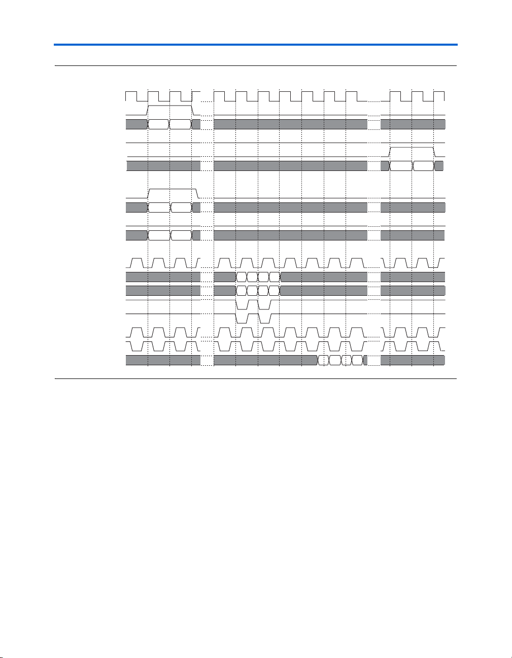
Figure 3–18. Simultaneous Read & Write—Burst of Two
51 52 52
0102 0304 0304
01 02 02
1112 1314 1314
51 01 52 02 02
11 12 13 14 14
01 02 03 04 04
avl_clk
avl_read
avl_adr_rd[19:0]
avl_wait_request_rd
avl_data_read_valid
avl_data_rd[17:0]
avl_write
avl_adr_wr[19:0]
avl_wait_request_wr
avl_data_wr[17:0]
qdrii_k
qdrii_a[19:0]
qdrii_d[17:0]
qdrii_wpsn
qdrii_rpsn
qdrii_cqn
qdrii_cq
qdrii_q[17:0]
Functional Description
Burst of Four (Wide Mode)
For the burst of four (wide mode) all the data is present in one clock cycle.
Similarly to the two cycles, you must alternate the read and write
commands on the QDRII SRAM interface. As a result, there is a pause
when both the read and write commands arrive simultaneously on the
Avalon interfaces. The first read is buffered and then the consecutive read
is delayed by one clock cycle, refer to Figure 3–19 on page 3–22.
Altera Corporation MegaCore Version 9.1 3–21
November 2009 QDRII SRAM Controller MegaCore Function User Guide
Page 54

Interfaces & Signals
Figure 3–19. Simultaneous Read & Write—Burst of Four (Wide Mode)
avl_clk
avl_read
avl_adr_rd[19:0]
avl_wait_request_rd
avl_data_read_valid
avl_data_rd[17:0]
avl_write
avl_adr_wr[19:0]
avl_wait_request_wr
avl_data_wr[17:0]
qdrii_k
qdrii_a[19:0]
qdrii_d[17:0]
qdrii_wpsn
qdrii_rpsn
qdrii_cqn
qdrii_cq
qdrii_q[17:0]
51 5252
01 0202
1234 56785678
51 01 52 0202
1 2 3 4 5 6 7 88
9 a b c d e f 00
9abc dfe0dfe0
Signals
Table 3–1 shows the system signals.
Table 3–1. System Signals (Part 1 of 2)
Signal Direction Description
avl_clk
avl_clk_wr
avl_resetn
dll_delay_ctrl[6]
3–22 MegaCore Version 9.1 Altera Corporation
QDRII SRAM Controller MegaCore Function User Guide November 2009
Input System clock derived from the PLL.
Input Write clock derived from the PLL.
Input Reset signal, which you can assert
asynchronously, but you must
deassert synchronously to
avl_clk.
Input Delay bus for DLL to shift DQS inputs.
DQS mode only.
Page 55

Table 3–2 shows the Avalon write signals.
Table 3–2. Avalon Write Signals
Signal Width (Bits) Direction Description
avl_addr_wr
avl_byteen_wr
avl_chipselect_wr
avl_data_wr
avl_write
avl_wait_request_
21 Input Avalon write address.
2, 4, 8, or 16 Input Byte enable (active low).
1 Input Device select for the write port.
18, 36, 72,
144, or 288
1 Input Avalon write request.
1 Output Avalon write wait—the transaction does not occur on this
wr
Table 3–1. System Signals (Part 2 of 2)
Signal Direction Description
non_dqs_capture
Input Non-DQS capture mode clock.
_clock
training_done
training_incorrec
Output Asserted when the training of the core
Output The core is nonfunctional.
t
training_pattern_
Output The core is nonfunctional. The
not_found
Input Avalon data write from master.
cycle.
Functional Description
is complete.
Asserted when the training reaches
the maximum number of iterations but
fails to adjust the pointers.
training must find a positive edge on
the bit 0 of data. The core did not find
this edge.
Table 3–3 shows the Avalon read signals.
Table 3–3. Avalon Read Signals (Part 1 of 2)
Signal Width (Bits) Direction Description
avl_addr_rd
avl_byteen_rd
avl_chipselect_rd
avl_read
avl_data_rd
Altera Corporation MegaCore Version 9.1 3–23
November 2009 QDRII SRAM Controller MegaCore Function User Guide
21 Input Avalon read address.
2 to 16 Input Byte enable (active low).
1 Input Device select for the read port.
1 Input Avalon read request.
18, 36, 72,
144, or 288
Output Avalon read data to master.
Page 56

Interfaces & Signals
Table 3–3. Avalon Read Signals (Part 2 of 2)
Signal Width (Bits) Direction Description
avl_datavalid_rd
avl_wait_request_
1 Output Avalon read data valid—the data is sent concurrent to
1 Output Avalon read wait—the transaction does not occur on this
rd
Table 3–4 shows the QDRII memory signals.
Table 3–4. QDRII Memory Signals
Signal Width (Bits) Direction Description
qdrii_a
qdrii_bwsn
qdrii_cq
qdrii_cqn
qdrii_d
qdrii_k
qdrii_kn
qdrii_q
qdrii_rpsn
qdrii_wpsn
the signal.
cycle.
21 Output Address bus.
8 Output Byte enable to memory.
9 Input Free running clock from memory.
9 Input Free running clock from memory.
72 Output Data out.
9 Output Free running clock to memory.
9 Output Free running clock to memory.
72 Input Data in from memory.
8 Output Read signal to memory. Active low
and reset in the inactive state.
8 Output Write signal to memory. Active low
and reset in the inactive state.
Table 3–5 shows the datapath interface signals.
Table 3–5. Datapath Interface Signals (Part 1 of 2)
Name
clk
control_a_rd
control_a_wr
control_bwsn
control_rpsn
control_wdata
3–24 MegaCore Version 9.1 Altera Corporation
QDRII SRAM Controller MegaCore Function User Guide November 2009
Width
(Bits)
– Input Clock.
17:0 Input Read address from the pipeline and resynchronization logic.
17:0 Input Write address from the pipeline and resynchronization logic.
3:0 Input Byte enable from the pipeline and resynchronization logic.
– Input Read from the pipeline and resynchronization logic.
35:0 Input Write data from the pipeline and resynchronization logic.
Direction Description
Page 57

Table 3–5. Datapath Interface Signals (Part 2 of 2)
Functional Description
Name
control_wpsn
dll_delay_ctrl
capture_clock
captured_data
Width
(Bits)
– Input Write signal from the pipeline and resynchronization logic.
5:0 Input
– Output Capture clocks (CQ into soft logic) to the pipeline and
35:0 Output Captured data—data after the IO to pipeline and
Direction Description
DLL delay control from the top-level design to shift the
nominal 90 degrees.
resynchronization logic.
resynchronization logic.
Table 3–6 shows the datapath.
Table 3–6. Pipeline & Resynchronization Logic Signals
Name
avl_control_a_rd
avl_control_a_wr
avl_control_bwsn
avl_control_rpsn
avl_control_wdata
avl_control_wpsn
capture_clock
captured_data
clk
reset
control_a_rd
control_a_wr
control_bwsn
control_rdata
control_rpsn
control_wdata
control_wpsn
training_done
Width
(Bits)
17:0 Input Read address from the control logic.
17:0 Input Write address from the control logic.
3:0 Input Byte enable from the control logic.
– Input Read from the control logic.
35:0 Input Write data from the control logic.
– Input Write from the control logic.
– Input Clocks from the datapath (CQ into soft logic).
35:0 Input Data captured by IO from datapath.
– Input Clock.
– Input Reset.
17:0 Output Read address to datapath.
17:0 Output Write address to datapath.
3:0 Output Byte enable to datapath.
35:0 Output Read data after resynchronization to control logic.
– Output Read to datapath.
35:0 Output Write data to datapath.
– Output Write to datapath.
– Output Initial training done to control logic.
Direction Description
CQ by a
Altera Corporation MegaCore Version 9.1 3–25
November 2009 QDRII SRAM Controller MegaCore Function User Guide
Page 58

Device-Level Configuration
Device-Level
Configuration
This section describes the following topics:
■ “PLL Configuration” on page 3–26
■ “Example Design” on page 3–27
■ “Constraints” on page 3–29
PLL Configuration
IP Toolbench creates up to two example PLLs in your project directory,
which you can parameterize to meet your exact requirements. IP
Toolbench generates the example PLLs with an input to output clock ratio
of 1:1 and a clock frequency you entered in IP Toolbench. In addition IP
Toolbench sets the correct phase outputs on the PLLs’ clocks. You can
edit the PLLs to meet your requirements with the altpll MegaWizard
Plug-In. IP Toolbench overwrites your PLLs in your project directory
unless you turn off the Reset PLL to default setting option.
The external clocks are generated using standard I/O pins in double data
rate I/O (DDIO) mode (using the altddio_out megafunction). This
generation matches the way in which the write data is generated and
allows better control of the skew between the clock and the data to meet
the timing requirements of the QDRII SRAM.
The PLL has the following outputs:
■ Output c0 drives the system clock that clocks most of the controller
including the state machine and the local interface.
■ Output c1 drives the write clock that lags the system clock by 90.
The recommended configuration for implementing the QDRII SRAM
controller in a Stratix series is to use a single enhanced PLL to produce all
the required clock signals. No external clock buffer is required as the
Altera device can generate clock signals for the QDRII SRAM devices.
For Stratix II devices, if you turn off DQS mode, you enable fed-back
resynchronization, which uses a fed-back clock to resynchronize the data.
Figure 3–20 on page 3–27 shows the recommended PLL configuration.
3–26 MegaCore Version 9.1 Altera Corporation
QDRII SRAM Controller MegaCore Function User Guide November 2009
Page 59

Figure 3–20. PLL Configuration
Optional
Fed-Back Clock
PLL (Note 2)
FPGA Device
QDRII SRAM
qdrii_k_n
qdrii_k
qdrii_cq
QDRII SRAM
Controller
altddio
clock_source
Enhanced PLL
clk
write_clk
non_dqs_
capture_clock
C0
C1
Stratix II DLL
(Note 1)
altddio
Notes to Figure 3–20:
(1) Stratix II devices only.
(2) Non-DQS mode only.
Functional Description
Example Design
IP Toolbench creates an example design that shows you how to
instantiate and connect up the QDRII SRAM controller. The example
design is a working system that can be compiled and used for both static
timing checks and board tests. It also instantiates an example PLL and
shows you how to generate the external clocks for the QDRII SRAM
device.
The example design consists of the QDRII SRAM controller, some driver
logic to issue read and write requests to the controller, and a PLL to create
the necessary clocks. The asynchronous reset, avl_resetn, drives the
reset logic, which resets the PLL and all the logic. When the PLL is locked
and avl_resetn is deasserted, the reset to the core, soft_reset_n, is
also deasserted. If the PLL lock is lost, the reset logic issues a reset.
Altera Corporation MegaCore Version 9.1 3–27
November 2009 QDRII SRAM Controller MegaCore Function User Guide
Figure 3–21 on page 3–28 shows the testbench and the example design.
Page 60

Device-Level Configuration
Example Driver
PLLref_clk
test_complete
pnf
Example Design
Testbench
QDRII SRAM Controller
QDRII SRAM
Model
DLL
Figure 3–21. Testbench & Example Design
Table 3–7 describes the files that are associated with the example design
and the testbench.
Table 3–7. Example Design & Testbench Files
Filename Description
<top-level name>_tb.v or .vhd (1) Testbench for the example design.
<top-level name>.vhd or .v (1) Example design.
qdrii_pll_stratixii.vhd Example PLL, which you should
<variation name>_example_driver.v
or .vhd (2)
<variation name> .v or .vhd (2) QDRII SRAM controller.
Notes to Ta b l e 3– 7 :
(1) <top-level name> is the name of the Quartus II project top-level entity.
(2) <variation name> is the is the name you give to the controller you create with the
Megawizard.
configure to match your frequency.
Example driver.
The example driver is a self-checking test generator for the QDRII SRAM
controller. It uses a state machine to write data patterns to all memory
banks. It then reads back the data and checks that the data matches. If a ny
read data fails the comparison, the fail output transitions high for one
cycle and the fail permanent output transitions high and stays high.
3–28 MegaCore Version 9.1 Altera Corporation
QDRII SRAM Controller MegaCore Function User Guide November 2009
The data patterns used are generated using an 8-bit counter per byte, with
each counter having a different initialization seed.
Page 61

Functional Description
The testbench instantiates a QDRII SRAM model, a reference clock for the
PLL, and model for the system board memory trace delays.
Altera provides a Verilog HDL simulation model. The model is a
behavioral model to verify the design but does not simulate any delays.
Altera recommends that you replace the model with the specific model
from your memory vendor.
f For more details on how to run the simulation script, refer to “Simulate
the Example Design” on page 2–11.
Constraints
IP Toolbench generates a constraints script,
add_constraints_for_<variation name>.tcl, which is a set of Quartus II
assignments that are required to successfully compile the example
design.
1 When the constraints script runs, it creates another script,
remove_constraints_for_<variation name>.tcl, which you can
use to remove the constraints from your design.
The constraints script implements the following types of assignments:
■ cqn, cq, and q capture pins placement
■ Capacitance loading
■ cq pin set to non-global signal
■ I/O type for all interface pins
■ Cut timing assignments for false timing paths
Parameters
Altera Corporation MegaCore Version 9.1 3–29
November 2009 QDRII SRAM Controller MegaCore Function User Guide
The parameters can only be set in IP Toolbench (refer to “Step 1:
Parameterize” on page 2–5).
Page 62

Parameters
Memory
Table 3–8 shows the memory type parameters.
Table 3–8. Memory Type Parameters
Parameter Value Description
Memory device Part number A part number for a particular
QDRII or
QDRII+
Clock speed Up to
300 MHz (1)
Voltage 1.5 or 1.8 V Memory device voltage.
Burst length 2/4 Burst length.
Data bus width 8, 9, 16, 18,
32, 36
Address bus width 15 to 23 Memory space.
Memory latency For QDRII,
1.5; for
QDRII+, 2.0
or 2.5
memory device. Choosing an entry
other than Custom sets many of the
parameters in the wizard to the
correct value for the specified part. If
any such parameter is changed to a
value that is not supported by the
specified device, the preset
automatically changes to custom.
You can add your own devices to
this list by editing the
memory_types.dat file in the
\constraints directory.
Selects QDRII or QDRII+ SRAM
devices.
The memory controller clock
frequency. The constraints script
and the datapath use this clock
speed. It must be set to the value
that you intend to use. The first time
you use IP Toolbench or if you turn
on Automatically generate the
PLL, it uses this value for the IP
Toolbench-generated PLL’s input
and output clocks .
QDRII SRAM device width.
The memory latency. QDRII+ is
bursts of four only.
Note to Ta b l e 3– 8 :
(1) IP Toolbench allows you to enter up to 600 MHz, but Altera only supports the
QDRII SRAM controller up to 300 MHz.
3–30 MegaCore Version 9.1 Altera Corporation
QDRII SRAM Controller MegaCore Function User Guide November 2009
Page 63

Functional Description
Table 3–9 shows the local bus width parameter (only available with burst
length of four).
Table 3–9. Local Bus Width Parameters
Parameter Value Description
Local bus width Narrow mode
or wide mode
Narrow mode is twice the width of
the memory; wide mode is four
times the width of the memory.
Table 3–10 shows the memory interface parameters.
Table 3–10. Memory Interface Parameters
Parameter Value Description
Device width 1 to 4 Specifies the number of devices to
increase the width of the data bus.
Device depth 1 to 2 Choose 2 to double the memory
space.
Use
altddio pin
On or off
When turned on altddio outputs
generate the clock outputs. Turn off
to use dedicated PLL outputs to
generate the clocks, which is
recommended for HardCopy II
devices.
Board & Controller
Table 3–11 shows the pipelining parameters.
Table 3–11. Pipelining Parameters
Parameter Value Description
Number of pipeline
registers on address,
command, and data
outputs
Number of pipeline
registers on read data
Altera Corporation MegaCore Version 9.1 3–31
November 2009 QDRII SRAM Controller MegaCore Function User Guide
0 to 4 You can choose 1, 2, or 3 pipeline registers between the memory
controller and the address, command, and data outputs. These
registers help to achieve the required performance at higher
frequencies.
0 to 4 You can choose 1, 2, or 3 pipeline registers between the memory
controller and the read data input. These registers help to achieve the
required performance at higher frequencies.
Page 64

Parameters
Table 3–12 shows the read latency options.
Table 3–12. Read Latency Options
Parameter Value Description
Manual read latency
setting
Set latency to clock cycle –2 < current
On or off Turn on if you want to choose the
latency clock cycle.
Choose the latency clock cycle. For
clock cycle <
+4
example, if the default is 13, you can
choose any value from 11 to 17.
However, Altera recommends that
you do not alter this parameter.
Table 3–13 shows the capture modes.
Table 3–13. Capture Modes
Parameter Value Description
DQS mode On or off Turn on for DQS capture mode (Stratix II devices only). The controller
is in non-DQS mode only for Stratix devices.
Use migratable byte
groups
On or off When turned on, you can migrate the design to a migration device
(Stratix II devices only). When turned off the wizard allows much
greater flexibility in the placement of byte groups.
Table 3–14 shows the pin loading parameters.
Table 3–14. Pin Loading Parameters
Parameter Range (pF) Description
Pin loading on data
pins
Pin loading on FPGA
address and
command pins
Pin loading on FPGA
clock pins
3–32 MegaCore Version 9.1 Altera Corporation
QDRII SRAM Controller MegaCore Function User Guide November 2009
Any Enter the pin loading to match your board and memory devices.
Any Enter the pin loading to match your board and memory devices.
Any Enter the pin loading to match your board and memory devices.
Page 65

Project Settings
Table 3–15 shows the example settings.
Table 3–15. Example Settings
Parameter Description
Automatically apply QDR
SRAM controller-specific
constraints to the
Quartus II project
Update the example
design file that
instantiates the QDRII
SRAM controller
variation
Update example design
system PLL
When this option is turned on, the next time you compile, the Quartus II software
automatically runs the add constraints script. Turn off this option if you do not want
the script to run automatically.
When this option is turned on, IP Toolbench parses and updates the example design
file. It only updates sections that are between the following markers:
<<START MEGAWIZARD INSERT <tagname>
<<END MEGAWIZARD INSERT <tagname>
If you edit the example design file, ensure that your changes are outside of the
markers or remove the markers. Once you remove the markers, you must keep the
file updated, because IP Toolbench can no longer update the file.
When this option is turned on, IP Toolbench automatically overwrites the PLL.Turn off
this option, if you do not want the wizard to overwrite the PLL. The first time you
create a custom variation, you must turn on Update example design system PLL.
Functional Description
Table 3–16 shows the variation path parameters.
Table 3–16. Variation Path Parameters
Parameter Description
Enable hierarchy control The constraints script analyzes your design, to automatically extract the hierarchy to
your variation. To prevent the constraints script analyzing your design, turn on
Enable hierarchy control, and enter the correct hierarchy path to your controller.
Hierarchy path to
variation
The hierarchy path is the path to your QDRII SRAM controller, minus the top-level
name. The hierarchy entered in the wizard must match your design, because the
constraints scripts rely on this path for correct operation.
Table 3–17 shows the pin prefixes parameter.
Table 3–17. Pin Prefixes
Parameter Description
Prefix all QDRII SRAM
pins with
Altera Corporation MegaCore Version 9.1 3–33
November 2009 QDRII SRAM Controller MegaCore Function User Guide
This string prefixes the pin names for the FPGA pins that are connected to the QDRII
SRAM controller.
Page 66

MegaCore Verification
MegaCore
MegaCore verification involves simulation testing and hardware testing.
Verification
Simulation Environment
Altera has carried out extensive tests using industry-standard models to
ensure the functionality of the QDRII SRAM controller. In addition,
Altera has carried out a wide variety of gate-level tests of the QDRII
SRAM controller to verify the post-compilation functionality of the
controller.
Hardware Testing
Table 3–18 shows the Altera development board on which Altera
hardware tested the QDRII SRAM controller.
Table 3–18. Altera Development Boards
Development Board Altera Device Memory Device
Stratix II Memory Demonstration Board 2 EP2S60F1020C3 Samsung 18-bit QDRII SDRAM
3–34 MegaCore Version 9.1 Altera Corporation
QDRII SRAM Controller MegaCore Function User Guide November 2009
Page 67

Additional Information
Revision History
The following table shows the revision history for the chapters in this user
guide.
Date Version Changes Made
November 2009 9.1 Updated the release information.
March 2009 9.0 Updated the release information.
November 2008 8.1 Updated the release information.
May 2008 8.0 Updated the device support.
October 2007 7.2 Added compilation timing tips.
May 2007 7.1
March 2007 7.0 No changes.
December 2006 6.1 Updated format.
How to Contact
● Updated the device support.
● Corrected burst of two timing diagram.
● Added information for new reset block in example design.
● Added new training signals and updated training group module description.
● Added extra resynchronization and pipeline logic information.
● Updated description of wpsn and rpsn signals.
For the most up-to-date information about Altera products, see the
following table .
Altera
Contact (1)
Technical suppor t Website www.altera.com/support
Technical training Website www.altera.com/training
Product literature Website www.altera.com/literature
Non-technical support (General) Email nacomp@altera.com
(Software Licensing) Email authorization@altera.com
Contact
Method
Email custrain@altera.com
Address
Note:
(1) You can also contact your local Altera sales office or sales representative.
Altera Corporation MegaCore Version 9.18.0 Info–i
November 2009
Page 68

Typographic Conventions
Typographic
The following table shows the typographic conventions that this
document uses.
Conventions
Visual Cue Meaning
Bold Type with Initial
Capital Letters
bold type Indicates directory names, project names, disk drive names, file names, file name
Italic Type with Initial Capital
Letters
Italic type Indicates variables. For example, n + 1.
Initial Capital Letters Indicates keyboard keys and menu names. For example, Delete key, and the
“Subheading Title” Quotation marks indicate references to sections within a document and titles of
Courier type
Indicates command names, dialog box titles, dialog box options, and other GUI
labels. For example, Save As dialog box.
extensions, and software utility names. For example, \qdesigns directory,
d: drive, and chiptrip.gdf file.
Indicates document titles. For example, AN 519: Stratix IV Design Guidelines.
Variable names are enclosed in angle brackets (< >). For example, <file name>
and <project name>.pof file.
Options menu.
Quartus II Help topics. For example, “Typographic Conventions.”
Indicates signal, port, register, bit, block, and primitive names. For example,
data1, tdi, and input. Active-low signals are denoted by suffix n. For
example,
Indicates command line commands and anything that must be typed exactly as
it appears. For example,
resetn.
c:\qdesigns\tutorial\chiptrip.gdf.
Also, indicates sections of an actual file, such as a Report File, references to
parts of files (for example, the AHDL keyword
names (for example,
1., 2., 3., and
a., b., c., etc.
● • Bullets indicate a list of items when the sequence of the items is not important.
■
1 The hand points to information that requires special attention.
c
w
r The angled arrow instructs you to press Enter.
f The feet direct you to more information about a particular topic.
Info–ii MegaCore Version 9.1 Altera Corporation
QDRII SRAM Controller MegaCore Function User Guide November 2009
Numbered steps indicate a list of items when the sequence of the items is
important, such as the steps listed in a procedure.
A caution calls attention to a condition or possible situation that can damage or
destroy the product or your work.
A warning calls attention to a condition or possible situation that can cause you
injury.
TRI).
SUBDESIGN), and logic function
 Loading...