

Page 1

2015.01.16
www.altera.com
101 Innovation Drive, San Jose, CA 95134
Altera PHYLite for Parallel Interfaces IP Core User
Guide
ug_altera_phylite
Subscribe
The Altera PHYLite for Parallel Interfaces IP core controls the strobe-based capture I/O elements in
Arria® 10 devices. Use each instance of the IP core to support an interface with up to 18 individual data/
strobe capture groups. Each group can contain up to 48 data I/Os as well as the strobe capture logic.
Device Family Support
The Altera PHYLite for Parallel Interfaces IP core supports Arria® 10 devices only.
For Arria V, Cyclone® V, and Stratix® V devices, use the ALTDQ_DQS2 IP core instead.
Related Information
• ALTDQ_DQS2 IP Core User Guide
For more information about the ALTDQ_DQS2 IP core
Features
The Altera PHYLite for Parallel Interfaces IP core:
• Supports input, output, and bidirectional data channels
• Supports DQS-group based data capture, with up to 48 I/Os (including strobes) per group and DQS
gating/ungating circuitry for strobe-based interfaces
• Supports output delays via interpolator
• Supports dynamic on-chip termination (OCT) control
• Supports quarter-rate to half-rate and half-rate to full-rate conversions. Also supports input, output,
and read/DQS/OCT enable paths
• Supports single data rate (SDR) and double data rate (DDR) at the I/Os
• Supports PHY clock tree
• Supports dynamically reconfigurable delay chains using Avalon interface
• Supports process, voltage, and temperature (PVT) or non-PVT compensated input and DQS delay
chains
Send Feedback
Note:
©
2015 Altera Corporation. All rights reserved. ALTERA, ARRIA, CYCLONE, ENPIRION, MAX, MEGACORE, NIOS, QUARTUS and STRATIX words and logos are
trademarks of Altera Corporation and registered in the U.S. Patent and Trademark Office and in other countries. All other words and logos identified as
trademarks or service marks are the property of their respective holders as described at www.altera.com/common/legal.html. Altera warrants performance
of its semiconductor products to current specifications in accordance with Altera's standard warranty, but reserves the right to make changes to any
products and services at any time without notice. Altera assumes no responsibility or liability arising out of the application or use of any information,
product, or service described herein except as expressly agreed to in writing by Altera. Altera customers are advised to obtain the latest version of device
specifications before relying on any published information and before placing orders for products or services.
The non-PVT compensated component of the input delay is not set in the Quartus II software
version 14.1 and will only be set in a future release of the Quartus II software.
ISO
9001:2008
Registered
Page 2
I/O Bank
I/O Bank
I/O Bank
I/O AUX
2
Overview
Overview
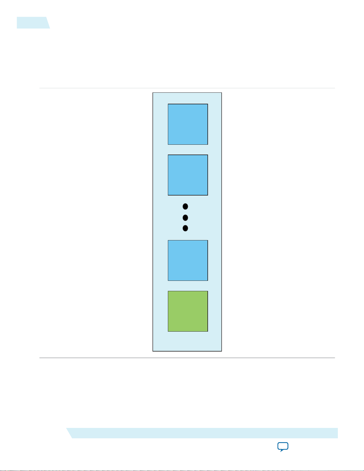
The Arria 10 I/O subsystem is located in the I/O columns. Each column consists of up to 13 I/O banks
and one I/O aux.
Figure 1: I/O Column for Arria 10 Devices
ug_altera_phylite
2015.01.16
Each bank is a group of 48 I/O pins, organized into four I/O lanes with 12 pins for each lane.
Altera Corporation
Altera PHYLite for Parallel Interfaces IP Core User Guide
Send Feedback
Page 3
2L
2K
2J
2I
2H
2G
2F
2A
3H
3G
3F
3E
3D
3C
3B
3A
Transceiver Block
Transceiver Block
HSSI
Column
I/O
Column
Tile
Control
I/O
Column
Individual
I/O Banks
LVDS I/O Buffer Pair
LVDS I/O Buffer Pair
LVDS I/O Buffer Pair
LVDS I/O Buffer Pair
LVDS I/O Buffer Pair
LVDS I/O Buffer Pair
SERDES & DPA
SERDES & DPA
SERDES & DPA
SERDES & DPA
SERDES & DPA
SERDES & DPA
I/O Lane
LVDS I/O Buffer Pair
LVDS I/O Buffer Pair
LVDS I/O Buffer Pair
LVDS I/O Buffer Pair
LVDS I/O Buffer Pair
LVDS I/O Buffer Pair
SERDES & DPA
SERDES & DPA
SERDES & DPA
SERDES & DPA
SERDES & DPA
SERDES & DPA
I/O Lane
I/O Center
I/O PLL
Hard Memory Controller
and
PHY Sequencer
I/O DLL I/O CLK
OCT VR
LVDS I/O Buffer Pair
LVDS I/O Buffer Pair
LVDS I/O Buffer Pair
LVDS I/O Buffer Pair
LVDS I/O Buffer Pair
LVDS I/O Buffer Pair
SERDES & DPA
SERDES & DPA
SERDES & DPA
SERDES & DPA
SERDES & DPA
SERDES & DPA
I/O Lane
LVDS I/O Buffer Pair
LVDS I/O Buffer Pair
LVDS I/O Buffer Pair
LVDS I/O Buffer Pair
LVDS I/O Buffer Pair
LVDS I/O Buffer Pair
SERDES & DPA
SERDES & DPA
SERDES & DPA
SERDES & DPA
SERDES & DPA
SERDES & DPA
I/O Lane
ug_altera_phylite
2015.01.16
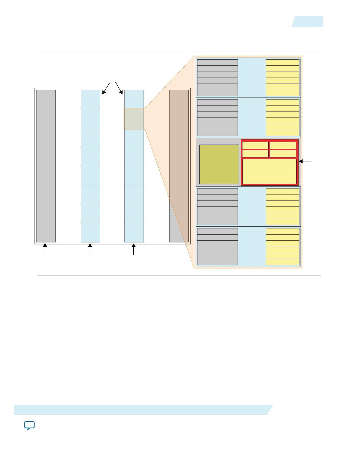
Figure 2: 48-I/O Banks in Arria 10 Devices
This figure shows a detailed view of the I/O bank in Arria 10 devices.
Clocks
3
Each I/O lane contains the DDR-PHY input and output path logic for 12 I/Os as well as a DQS logic
block. All four lanes in a bank can be combined to form a single data/strobe group or up to four groups in
the same interface. Under certain conditions, two groups from different interfaces can also be supported
in the same bank.
Related Information
• Placement Restrictions on page 15
For more information about placement restrictions
• Functional Description—Arria 10 EMIF
For more information about the architecture
Clocks
The Altera PHYLite for Parallel Interfaces IP core uses four clock domains for the output and input paths.
Refer to Figure 4 for the clock domain boundaries.
Altera PHYLite for Parallel Interfaces IP Core User Guide
Send Feedback
Altera Corporation
Page 4
VCO Clock Frequency : External Memory Clock Frequency : Core/PHY Clock Frequency
VCO Frequency Multiplier User Specified Core Clock Rate
4
Clock Frequency Relationships
Clock Domain Description
Core clock This clock is generated internally by the IP core and output to the core to be used for
all transfers between the FPGA core and the IP core.
PHY Clock This clock is used internally by the IP core for PHY circuitry running at the same
frequency as the core clock. The PHY circuitry ensures that this clock is kept in phase
with the core clock for core-to-periphery and periphery-to-core transfers.
VCO clock This clock is generated internally by the PLL. It is used by both the input and output
paths to generate PVT compensated delays.
ug_altera_phylite
2015.01.16
External Memory
Clock
This is the user specified frequency at which the FPGA I/Os connected to the
external device operate.
Clock Frequency Relationships
Figure 3: Clock Frequency Relationships
VCO Frequency Multiplication Factor
The relationship between the VCO clock frequency and the user specified external memory clock
frequency is calculated during generation of the IP core based on the this table.
Table 1: VCO Frequency Multiplication Factor
VCO
Frequency
Multiplication
Factor
Speed Grade -1 Speed Grade -2 Speed Grade -3
Minimum
Frequency
Maximum
Frequency
Minimum
Frequency
Maximum
Frequency
Minimum
Frequency
1 600 800 600 800 550 800
2 300 600 300 600 275 550
4 150 300 150 300 137.5 275
8 100 150 100 150 100 137.5
Altera Corporation
Altera PHYLite for Parallel Interfaces IP Core User Guide
Maximum Frequency
Send Feedback
Page 5
PLL
I/O Lane
I/O Lane
Tile Control
I/O Lane
I/O Lane
VCO/Interpolator
phy_clk
phy_clk_phs
core_clk_out
data_in/out/io
data_in/out/io
Data to/from Core
Group
ref_clk
Reference Clock
Core Clock
PHY Clock
ExternalClock
Legend
ug_altera_phylite
2015.01.16
Interface
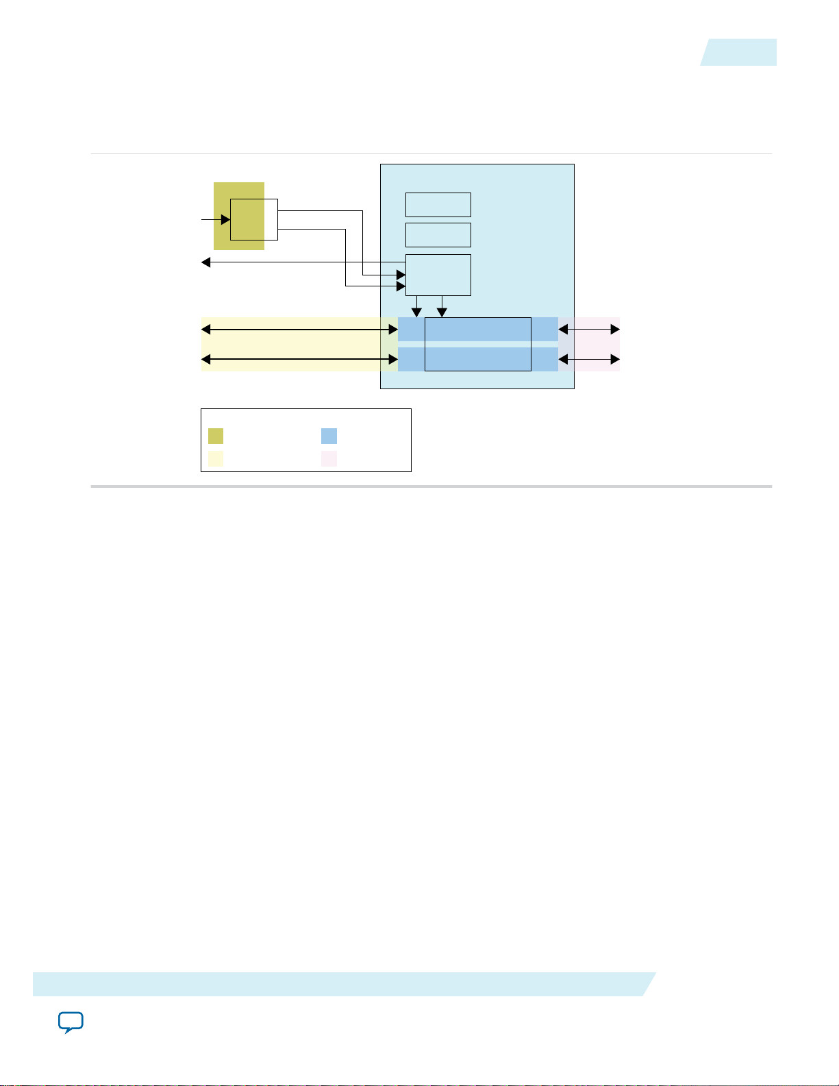
Figure 4: Top-Level Interface
Interface
This figure shows the top-level diagram of the Altera PHYLite for Parallel Interfaces IP core interface.
5
The Altera PHYLite for Parallel Interfaces IP core consists of the following interfaces:
• Clocks and Reset
• Core Data and Control (broken down into input and output paths)
• I/O (broken down into input and output paths)
• Avalon Configuration Bus
Related Information
• Output Path on page 5
For more information about the output path
• Input Path on page 8
For more information about the input path
• Signals on page 37
For more information about core data, control, and I/O interfaces signals
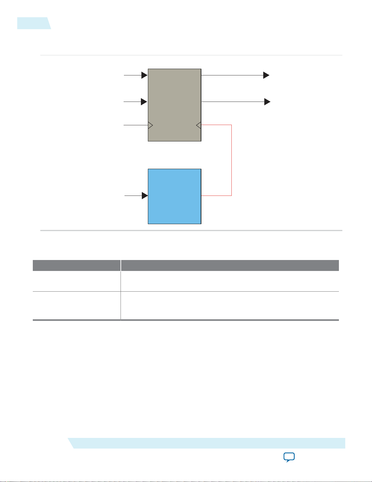
Output Path
The output path consists of a FIFO and an interpolator.
Altera PHYLite for Parallel Interfaces IP Core User Guide
Send Feedback
Altera Corporation
Page 6
Write FIFO
data_io
data_out
oe_out
oct_out
Interpolator
interpolator_clk
data_from_core
oe_from_core
phy_clk
VCO clock
output_strobe_in
output_strobe_en
strobe_out
strobe_io
6
Output Path
Figure 5: Output Path
This figure shows the output path for the Altera PHYLite for Parallel Interfaces IP core.
ug_altera_phylite
2015.01.16
Table 2: Blocks in Output Path
This table lists the blocks in the output path.
FIFO Serializes the output data from the core with a serialization factor of up to 8
Interpolator Works with the FIFO block to generate the desired output delay. You can
Block Description
(in DDR quarter-rate).
dynamically configure the delay through the Avalon interface. For more
information, refer to Dynamic Reconfiguration on page 20.
Altera Corporation
Altera PHYLite for Parallel Interfaces IP Core User Guide
Send Feedback
Page 7
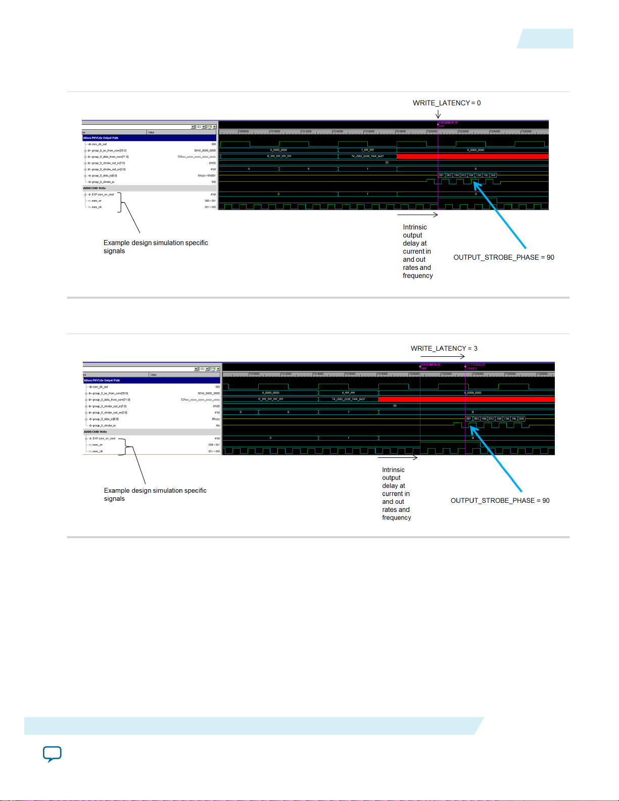
ug_altera_phylite
2015.01.16
Figure 6: Output Path - Write Latency 0
Figure 7: Output Path - Write Latency 3
These figures show the waveform diagrams for the output path.
Output Path Data Alignment
7
Related Information
Output Path Signals on page 38
For more information about output path signals
Output Path Data Alignment
The data_from_core and oe_from_core signals are arranged in time slices, which are broken down into
the individual pins in the group. The first time slice is on the LSBs of the busses, which matches the Altera
PHY interface (AFI) bus ordering of the Arria 10 External Memory Interfaces IP core.
{...,time2,time1,time0}
Where time0 = {...,pin1,pin0}
Altera PHYLite for Parallel Interfaces IP Core User Guide
Send Feedback
Altera Corporation
Page 8
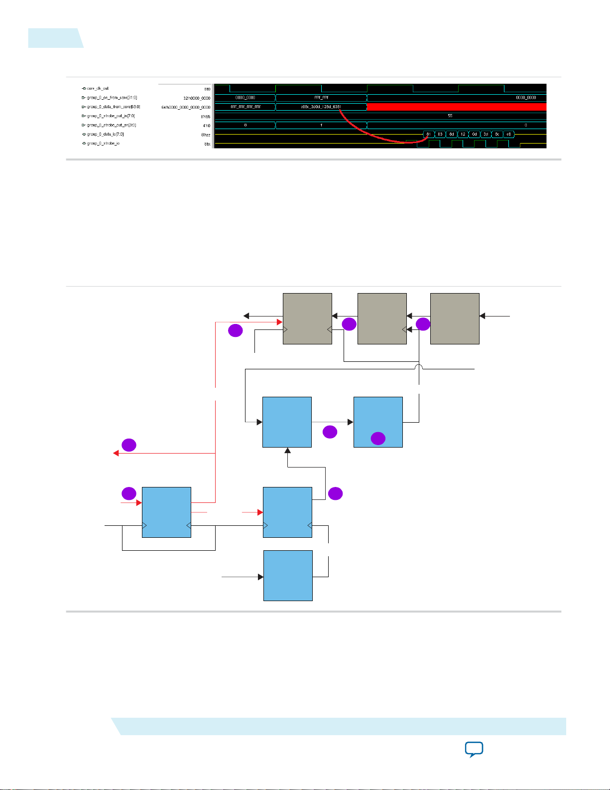
Read FIFO DDIO
Delay Chain
(PVT)
data_to_core
data_in
phy_clk
strobe_in
dqs
Delay Chain
(PVT)
dqs_clean
pstamble_reg
FIFO
Interpolator
interpolator_clk
dqs_enable
phy_clk_phs
VFIFO
read_enable
dqs_enable
rdata_en
phy_clk
rdata_valid
data_io
strobe_io
strobe_in_n
6
1
2
3
4
5 5
6
8
Input Path
Figure 8: Example Output for Quarter Rate DDR
Related Information
• External Memory Interface Handbook
For more information about the AFI 3.0 specification
Input Path
Figure 9: Input Path
This figure shows the input path of the IP core.
ug_altera_phylite
2015.01.16
Altera Corporation
The input path of the IP core consists of a data path, a strobe path, and read enable path.
Altera PHYLite for Parallel Interfaces IP Core User Guide
Send Feedback
Page 9

ug_altera_phylite
2015.01.16
Table 3: Blocks in Data, Strobe, and Read Enable Paths
This table lists the information about these paths.
Path Description
Data Path Consists of a PVT compensated delay chain, a DDIO and a read FIFO.
• PVT compensated delay chain—Allows per-bit deskew. You can only control the
PVT compensated delay chain over Avalon-MM interface. For more information,
refer to Dynamic Reconfiguration.
• DDIO and read FIFO—Responsible for deserialization with a factor of up to 8 (in
DDR quarter-rate). The transfer between the DDIO and the read FIFO is a zerocycle transfer.
The IP core supports SDR input by dropping every other bit of data going to the core.
Strobe Path Consists of pstamble_reg (a gating component) and a PVT compensated delay chain.
• pstamble_reg—This gating circuitry ensures that only clock edges associated with
valid input data are used.
• PVT compensated delay chain—Provides a phase offset between the strobe and the
data (for example, center aligning edge-aligned inputs).
Input Path
9
Read Enable Path Consists of VFIFO, FIFO, and an interpolator.
• VFIFO—takes the rdata_en signal from the core and delays it separately for two
outputs, one for the read enable on the read FIFO, and one for the strobe enable.
These delays are calculated at generation time based on the read latency that you
provide. Individual control is not necessary, but if you are modifying these delays
you can do so individually using dynamic reconfiguration.
• FIFO and interpolator—used for the strobe enable delay, the FIFO and interpo‐
lator are identical to the FIFO and interpolator circuitry in the output path. The
FIFO and interpolator are configured to match the output delay for a group with
no additional output delay (Write latency = 0). During dynamic reconfiguration,
the FIFO and interpolator can be used for fine grained control of the strobe enable
signal. Both of these delays are controlled by the Read latency parameter for the
group.
Table 4: Read Operation Sequence
A read operation is performed as listed in this table.
Legend in Figure 9 Operation
1 The core asserts the read_en signal (and the external device is issued a read
command)
2 The strobe enable is delayed through the two FIFOs by the programmed read latency
(which should match the latency of the external device)
3 The strobe signal is ungated by the strobe enable signal as valid data enters the read
path
Altera PHYLite for Parallel Interfaces IP Core User Guide
Send Feedback
Altera Corporation
Page 10

10
Input Path Data Alignment
Legend in Figure 9 Operation
4 The strobe is optionally delayed to create a phase offset between the strobe and the
input data (for example, 90° phase shift for DDR center-alignment)
5 The data is clocked into the DDIO and read FIFO by the strobe
6 The VFIFO asserts the read enable on the read FIFO and the rdata_valid signal to
the core simultaneously. This outputs the captured data and the associated valid signal
to the core.
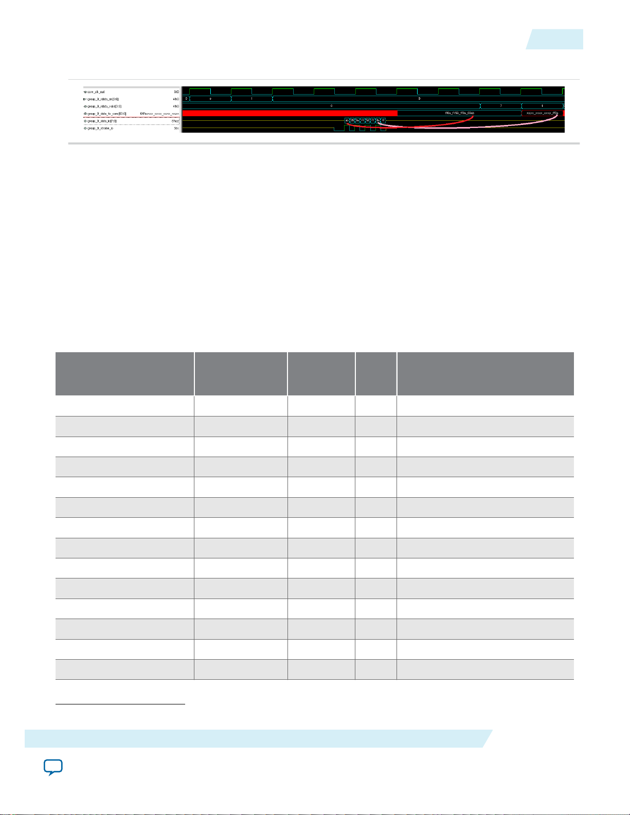
Figure 10: Input Path Waveform
This figure shows a waveform diagram of the input path.
ug_altera_phylite
2015.01.16
Related Information
Input Path Signals on page 40
For more information about input path signals
Input Path Data Alignment
The bus ordering of data_to_core, rdata_en, and rdata_valid is identical to the ordering of the output
path. That is, the LSBs of the bus hold the first time slice of data received.
The rdata_valid delay is always set by the IP core to match the rdata_en alignment. For example,
quarter-rate delays are multiples of four external memory clock cycles (one quarter rate clock cycle).
Unaligned reads will result in unaligned rdata_valid and data_to_core with data and valid signals
packed to the LSBs.
Figure 11: Example Input (Quarter Rate DDR) - Aligned
Altera Corporation
Altera PHYLite for Parallel Interfaces IP Core User Guide
Send Feedback
Page 11
ug_altera_phylite
2015.01.16
Figure 12: Example Input (Quarter Rate DDR) - Unaligned
I/O Standards
I/O Standards
11
The Altera PHYLite for Parallel Interfaces IP core allows you to set I/O standards on the pins associated
with the generated configuration. The I/O standard controls the available strobe configurations and OCT
settings for all groups.
When you select an I/O standard in the I/O standard parameter, the reference clock assigns the I/O
standard as a single-ended input. For a differential reference clock, override the single-ended Quartus II
IP File (.qip) setting in the .qsf.
If you want to assign I/O standards manually at the system level (in the .qsf), then set the I/O standard to
none, which will not output any I/O standard related .qip assignments from the IP generation.
Table 5: I/O Standards
I/O Standard Valid Input
Terminations (Ω)
Valid Output
(1)
Terminations
(Ω)
RZQ
(Ω)
(1)
Differential/Complementary I/O
SSTL-12 60, 120 40, 60 240 Yes
SSTL-125 20, 30, 40, 60, 120 34, 40 240 Yes
SSTL-135 20, 30, 40, 60, 120 34, 40 240 Yes
SSTL-15 20, 30, 40, 60, 120 34, 40 240 Yes
SSTL-15 Class I 0, 50 0, 50 100 Yes
SSTL-15 Class II 0, 50 0, 25 100 Yes
SSTL-18 Class I 0, 50 0, 50 100 Yes
SSTL-18 Class II 0, 50 0, 25 100 Yes
1.2-V HSTL Class I 0, 50 0, 50 100 Yes
1.2-V HSTL Class II 0, 50 0, 25 100 Yes
1.5-V HSTL Class I 0, 50 0, 50 100 Yes
1.5-V HSTL Class II 0, 50 0, 25 100 Yes
Support
1.8-V HSTL Class I 0, 50 0, 50 100 Yes
1.8-V HSTL Class II 0, 50 0, 25 100 Yes
(1)
0 is equivalent to none.
Altera PHYLite for Parallel Interfaces IP Core User Guide
Send Feedback
Altera Corporation
Page 12
12
Input Buffer Reference Voltage (VREF)
ug_altera_phylite
2015.01.16
I/O Standard Valid Input
Terminations (Ω)
1.2-V POD 34, 40, 48, 60, 80,
Valid Output
(1)
Terminations
(Ω)
(1)
RZQ
(Ω)
Differential/Complementary I/O
34, 40, 48, 60 240 Yes
120, 240
1.2-V — — — No
1.5-V — — — No
1.8-V — — — No
Input Buffer Reference Voltage (VREF)
The 1.2-V POD I/O standard allows a configurable VREF. By default, the externally provided VREF is
used and using an internal VREF requires the following .qsf assignments:
set_instance_assignment -name VREF_MODE <mode> -to <pin_name>
Note: The VREF settings are at the lane level, so all pins using a lane must have the same VREF settings
(including GPIOs).
Table 6: VREF_MODE Description
Support
VREF Mode Description
EXTERNAL Use the external VREF. This is the default.
CALIBRATED Use internal VREF generated using VREF codes from the Avalon reconfiguration bus.
VCCIO_45 Use internal VREF generated using static VREF code. VREF is 45% of VCCN
VCCIO_50 Use internal VREF generated using static VREF code. VREF is 50% of VCCN
VCCIO_55 Use internal VREF generated using static VREF code. VREF is 55% of VCCN
VCCIO_65 Use internal VREF generated using static VREF code. VREF is 65% of VCCN
VCCIO_70 Use internal VREF generated using static VREF code. VREF is 70% of VCCN
VCCIO_75 Use internal VREF generated using static VREF code. VREF is 75% of VCCN
(1)
0 is equivalent to none.
Altera Corporation
Altera PHYLite for Parallel Interfaces IP Core User Guide
Send Feedback
Page 13

Input Buffer
+
-
Vref
R
R
VCCN
Internal VREF
6 bits binary weighted resistors dividor
6 bits Static VREF Code
6 bits calibrated VREF code from Avalon bus
VREF Calibration Block
+
-
VCCN
Rt
External VREF
Resistor
Ladder
ug_altera_phylite
2015.01.16
Figure 13: VREF
Calibrated VREF Settings
13
Calibrated VREF Settings
Table 7: Calibrated VREF Settings
This table lists the calibrated VREF settings that you can set over the Avalon calibration bus.
avl_writedata[5:0] % of VCCN
000000 60.00%
000001 60.64%
000010 61.28%
000011 61.92%
000100 62.56%
Altera PHYLite for Parallel Interfaces IP Core User Guide
Send Feedback
Altera Corporation
Page 14

14
Calibrated VREF Settings
avl_writedata[5:0] % of VCCN
000101 63.20%
000110 63.84%
000111 64.48%
001000 65.12%
001001 65.76%
001010 66.40%
001011 67.04%
001100 67.68%
001101 68.32%
001110 68.96%
001111 69.60%
010000 70.24%
010001 70.88%
ug_altera_phylite
2015.01.16
010010 71.52%
010011 72.16%
010100 72.80%
010101 73.44%
010110 74.08%
010111 74.72%
011000 75.36%
011001 76.00%
011010 76.64%
011011 77.28%
011100 77.92%
011101 78.56%
011110 79.20%
011111 79.84%
100000 80.48%
Altera Corporation
100001 81.12%
100010 81.76%
100011 82.40%
Altera PHYLite for Parallel Interfaces IP Core User Guide
Send Feedback
Page 15
ug_altera_phylite
2015.01.16
Placement Restrictions
avl_writedata[5:0] % of VCCN
100100 83.04%
100101 83.68%
100110 84.32%
100111 84.96%
101000 85.60%
101001 86.24%
101010 86.88%
101011 87.52%
101100 88.16%
101101 88.80%
101110 89.44%
101111 90.08%
110000 90.72%
15
110001 91.36%
110010 92.00%
110011 -> 111111 Reserved
Related Information
Dynamic Reconfiguration on page 16
For more information on the Avalon bus usage
Placement Restrictions
Group Pin Placement
Place each group in the interface into a set of lanes in the same bank, the number of which depends on the
number of pins used by the group. All groups in an interface must be placed across a contiguous set of
banks.
Table 8: Group Pin Placement
Number of Pins in Group Valid DQS Group in a Bank Valid Indices in a Bank
1-12 DQS for X8/X9 {0-11}/{12-23}/{24-35}/{36-47}
13-24 DQS for X16/X18 {0-23}/{24-47}
24-48 DQS for X32/X36 {0-47}
Altera PHYLite for Parallel Interfaces IP Core User Guide
Send Feedback
Altera Corporation
Page 16

16
Reference Clock
Related Information
• Device Pin-Out File
For specific DQS group numbers refer to the specific device Pin-Out file
Reference Clock
The reference clock must be placed on a clock input in one of the banks used by the interface. If the
reference clock is used for multiple interfaces (consisting of a combination of EMIF and Altera PHYLite
for Parallel Interfaces IPs), it can be placed in any bank used by any of the interfaces, but the banks for all
interfaces must be contiguous.
Constraining Multiple Altera PHYLite for Parallel Interfaces to One I/O Bank
To constrain groups from separate Altera PHYLite for Parallel Interfaces IP core instances into the same
I/O bank, the instances must share the same reference clock and reset sources, the same external memory
frequencies and the same voltage settings.
Dynamic Reconfiguration
If you are using the dynamic reconfiguration feature, all interfaces of the Arria 10 External Memory
Interfaces and Altera PHYLite for Parallel Interfaces IP cores in the same I/O column must share the
reset signal. Multiple IP cores requiring Avalon core access require daisy chain connectivity.
ug_altera_phylite
2015.01.16
Related Information
Daisy Chain on page 20
Describes the daisy chain connectivity
Timing
The Quartus II software version 14.1 generates the required timing constraints to analyze the timing of
the Altera PHYLite for Parallel Interfaces IP core on the Arria 10 device.
Altera Corporation
Altera PHYLite for Parallel Interfaces IP Core User Guide
Send Feedback
Page 17

ug_altera_phylite
2015.01.16
Timing Components
Table 9: Timing Components
Timing Components
17
Circuit Category Timing
Source Synchronous
Read Path Memory
and optionally
calibrated
Source Synchronous
(2)
Write Path FPGA DQ/
and optionally
calibrated
(2)
Paths
Source Destination Description
Device
DQ Capture
Register
Source synchronous timing paths—
paths where clock and data signals are
passed from the transmitting devices
to the receiving devices.
Optionally calibrated paths—paths
DQS
Memory
Device
with delay elements that are
dynamically reconfigurable to achieve
timing closure, especially at higher
frequency, and to maximize the
timing margins. You can calibrate
these paths by implementing an
algorithm and turning on the
optional dynamic reconfiguration
feature. An example of the calibrated
path is the FPGA to memory device
write path, in which you can
dynamically reconfigure the delay
elements to, for instance, compensate
the skew due to process voltage
temperature variation.
Internal FPGA Core to
PHYLite
Core
Registers
Path
Internal FPGA PHYLite to
Read FIFO Core
Core
Timing Constraints and Files
To enable you to successfully timing constrain the Altera PHYLite for Parallel Interfaces IP core, the IP
core generates a set of timing files. You can locate these timing files in the <variation_name> directory:
• <variation_name> .sdc
• <variation_name> _ip_parameters.tcl
• <variation_name> _pin_map.tcl
(2)
Can be optionally calibrated by using dynamic reconfiguration.
Write FIFO
The internal FPGA paths are paths in
the FPGA fabric. The TimeQuest
timing analyzer reports the
corresponding timing margins.
Registers
Altera PHYLite for Parallel Interfaces IP Core User Guide
Send Feedback
Altera Corporation
Page 18

18
<variation_name>.sdc
<variation_name>.sdc
You can find the location of the <variation_name>.sdc file in the .qip, which is generated during the IP
generation. The <variation_name>.sdc allows the Fitter to optimize timing margins with timing driven
compilation and allows the TimeQuest timing analyzer to analyze the timing of your design.
The IP core uses <variation_name>.sdc for the following operations:
• Creating clocks on PLL inputs
• Creating generated clocks
• Calling derive_clock_uncertainty
• Creating set_output_delay and set_input_delay constraints to analyze the timing of the read and
write paths
<variation_name>_ip_parameters.tcl
The <variation_name>_ip_parameters.tcl file lists the Altera PHYLite for Parallel Interfaces IP core
parameters and is read by the <variation_name>.sdc.
<variation_name>_pin_map.tcl
The <variation_name>_pin_map.tcl is a TCL library of functions and procedures that
<variation_name>.sdc uses.
ug_altera_phylite
2015.01.16
Timing Analysis
Table 10: Timing Analysis
This table lists the timing analysis performed in the I/O and FPGA for the Altera PHYLite for Parallel Interfaces
IP core.
Location Description
I/O The Altera PHYLite for Parallel Interfaces IP core generation creates the appropriate
generated clock settings for the read strobe on the read path and the write strobe of the write
path, according to their strobe type (singled-ended, complementary, or differential) and their
interface type (SDR or DDR) in the following format:
• Clock name for read strobe—<pin_name>_IN.
• Clock name for the write path—<pin_name> for positive strobe.
• Clock name for the write path—<pin_name>_neg for negative strobe.
The set_false_path, set_input_delay and set_output_delay constraints are also
generated to ensure proper timing analysis of the Altera PHYLite for Parallel Interfaces IP
core.
Altera Corporation
Altera PHYLite for Parallel Interfaces IP Core User Guide
Send Feedback
Page 19

ug_altera_phylite
2015.01.16
Location Description
FPGA The Altera PHYLite for Parallel Interfaces IP core generation creates the clock settings for the
user core clock and the periphery clock in the following formats:
• user core clock—<variation_name>_usr_clk
• periphery clock— <variation_name>_phy_clk*
The user core clock is for user core logic and the periphery clock is the clock for the PHYLite
periphery hardware. With these clock settings, the TimeQuest Timing Analyzer analyzes the
timing of the Altera PHYLite for Parallel Interfaces IP core interface transfer and within core
transfer correctly.
Timing Closure Guidelines
Timing Closure: Dynamic Reconfiguration
You can dynamically reconfigure the delay elements in the I/O to optimize process, voltage, temperature
variations by implementing a calibration algorithm that modifies the input and output delays (refer to
Dynamic Reconfiguration on page 20).
Timing Closure Guidelines
19
The SDC cuts the I/O transfer paths and you must verify the reconfiguration algorithm to ensure that
your I/O transfers are working. The Quartus II software issues the following critical warning:
Dynamic Reconfiguration is ON but user has not set var(dynamic_reconfiguration_algorithm_verified) to 1. Please set to 1 after calibration algorithm is
extensively verified. I/O timing analysis may not represent the system.
After verifying the algorithm, you can disable the critical warning by editing the .sdc file and set the
following variable to 1:
var(dynamic_reconfiguration_algorithm_verified)
Timing Closure: Non Edge-Aligned Input Data
If the input data is not edge-aligned, modify the timing settings of the group to match the system. Convert
input strobe phase shift to nanosecond and subtract it from Input Strobe Setup Delay Constrain and
Input Strobe Hold Delay Constrain parameters.
If the input data is center-aligned with the input strobe, subtract the 90° phase shift from the Input Strobe
Setup Delay Constrain and Input Strobe Hold Delay Constrain parameters in the
<variation_name>.sdc. For example, if the memory speed is 800 MHz and the value of the Input Strobe
Setup Delay Constrain parameter is 0.1, change the value to 0.1-1.25*(90/360) = -0.2125.
Note:
Ensure that you make the changes in the Input Strobe Setup Delay Constrain and Input Strobe
Hold Delay Constrain parameters.
I/O Timing Violation
At high frequency configuration, it is difficult to achieve timing closure at I/O. Consider using the Arria
10 External Memory Interface IP core or the dynamic reconfiguration feature to calibrate the I/O path.
Altera PHYLite for Parallel Interfaces IP Core User Guide
Send Feedback
Altera Corporation
Page 20

20
Internal FPGA Path Timing Violation
Related Information
Dynamic Reconfiguration on page 20
For more information about using the dynamic reconfiguration feature to calibrate the I/O path
Internal FPGA Path Timing Violation
If timing violations are reported at the internal FPGA paths (such as <instance_name>_usr_clk or
<instance_name>_phy_clk_*), consider the following guidelines:
If setup time violation is reported, lower the clock rate of the user logic from full-rate to half-rate, or from
half-rate to quarter-rate. This reduces the frequency requirement of the IP core-to-core data transfer.
If hold time violation is observed, overconstrain the hold uncertainty in the .sdc to force the Fitter to fix
the hold time violation. Under normal circumstances, the Fitter should already attempt to avoid hold time
violation. It is possible that the Fitter may think adding more delay to avoid hold time at the fast timing
corner may cause setup time violation at the slow corner.
Dynamic Reconfiguration
Due to the asynchronous nature of the PHY, you must perform calibration to achieve timing closure at a
high frequency. At a high level, calibration involves reconfiguring input and output delays in the PHY to
align data and strobes. Enabling dynamic reconfiguration in the Altera PHYLite for Parallel Interfaces IP
core provides allows you to modify these delays using an Avalon-MM interface.
ug_altera_phylite
2015.01.16
RTL Connectivity
When generating the Altera PHYLite for Parallel Interfaces IP core with the dynamic reconfiguration
feature enabled, the Altera PHYLite for Parallel Interfaces IP core exposes the Avalon-MM master and
Avalon-MM slave interfaces. If the generated IP core is the only Altera PHYLite for Parallel Interfaces IP
core (with dynamic reconfiguration) or Arria 10 External Memory Interfaces IP core in the I/O column,
then only the slave interface needs to be used with a master in the core. Otherwise, both interfaces must be
connected as described in the following section.
Daisy Chain
The I/O column provides a single physical Avalon-MM interface. All IP cores in the I/O column that
require Avalon access from the core use the same physical Avalon-MM interface. The system level RTL
for the column reflects this resource limitation by using a daisy chain to connect all dynamically reconfig‐
urable IP cores in an I/O column.
The Altera PHYLite for Parallel Interfaces IP core exposes a 28-bit Avalon-MM address, where the top 4bits are the ID of the interface to be addressed in the daisy chain. These bits are only required for the daisy
chain arbitration in RTL simulation, so they are synthesized away during compilation. If only one
interface is addressed from the core, it is sufficient to tie these bits off to the interface’s ID.
Altera Corporation
Altera PHYLite for Parallel Interfaces IP Core User Guide
Send Feedback
Page 21

ug_altera_phylite
2015.01.16
Figure 14: Logical RTL View to Physical Column Placement
Addressing
21
This figure shows an example of a daisy chain consisting of the Arria 10 External Memory Interfaces and
Altera PHYLite for Parallel Interfaces IP cores before and after placement.
Notice that all core controllers must go through the arbitration logic that you created in the FPGA core
logic to connect to an interface on the daisy chain. The end of the daisy chain should have its master
output interface tied off.
Note:
Addressing
Each reconfigurable feature of the interface has an associated memory address. However, this address is
placement dependent so addresses of the interface lanes, as well as the pins must be tracked in order to
use the IP in a column that can be shared with other Altera PHYLite for Parallel Interfaces and the Arria
10 External Memory Interfaces IP cores, which also use the Avalon Bus.
Note:
The prefit netlist of a design using the daisy chain will not simulate correctly due to the rearrange‐
ment of the Avalon address pins, which is done by the Fitter. The postfit netlist will properly
simulate the merged I/O column.
Addressing is done at the 32-bit word boundary; avl_address[1:0] = 00
Altera PHYLite for Parallel Interfaces IP Core User Guide
Send Feedback
Altera Corporation
Page 22

22
Addressing
Table 11: Address Map
Feature Avalon Address R/WAddress CSR R Control Value
Field Range
ug_altera_phylite
2015.01.16
Pin Output
Phase
{id[3:0],
3'h2,lane_
addr[7:0],pin{4
:0],8'D0}
{id[3:0],
3'h2,lane_
addr[7:0],
4'hC,lgc_
sel[1:0],pin_
off[2:0],4'h0}
{id[3:0],
3'h1,lane_
addr[7:0],pi
n{4:0],8'E8}
Phase Value 12..0
Reserved 31..13
Delay Value 8..0
Reserved 11..9
Enable 12
Reserved 31..13
Minimum Setting: Refer
to Table 12
Maximum Setting: Refer
to Table 12
Incremental Delay: 1/
128th VCO clock period
The pin
output phase
switches
from the CSR
value to the
Avalon value
after the first
Note:
Avalon write.
It is only
reset to the
CSR value on
a reset of the
interface.
Pin PVT
Compensa
ted Input
Delay
Altera Corporation
• lgc_sel[1:0] is:
• 2'b01 for pin
<=5
• 2'b10 for pin
> 5
• pin_off[2:0] is:
• pin[2:0] for
pin <= 5
• pin[2:0] 3'h6 for pin
> 5
Not supported
Minimum Setting: 0
Maximum Setting: 511
VCO clock periods
Incremental Delay: 1/
256th VCO clock period
Altera PHYLite for Parallel Interfaces IP Core User Guide
Send Feedback
Page 23

ug_altera_phylite
2015.01.16
Feature Avalon Address R/WAddress CSR R Control Value
Field Range
Addressing
23
Strobe
PVT
compensat
ed input
(3)
delay
Strobe
enable
(3)
phase
{id[3:0],
3'h2,lane_
addr[7:0],
4'hC,lgc_
sel[1:0],
3'h6,4'h0}
• lgc_sel[1:0] =
• 2'b01 for a
• 2'b10 for b
(4)
{id[3:0],
3'h2,lane_
addr[7:0],
4'hC,lgc_
sel[1:0],
3'h7,4'h0}
• lgc_sel[1:0]
is:
• 2'b01 for a
• 2'b10 for b
(4)
Not supported
• {id[3:0],
3'h1,lane_
addr[7:0],
4'hC,
9'h194}
• {id[3:0],
3'h1,lane_
addr[7:0],
4'hC,
9'h198}
Delay Value 9..0
Reserved 11..10
Enable 12
Reserved 31..13
Phase Value 12..0
Reserved 14..13
Enable 15
Reserved 31..16
Minimum Setting: 0
Maximum Setting: 1023
VCO clock periods
Incremental Delay: 1/
256th VCO clock period
Minimum Setting: Refer
to Table 12
Maximum Setting: Refer
to Table 12
Incremental Delay: 1/
128th VCO clock period
Strobe
enable
(3)
delay
(3)
Modifying these values must be done on all lanes in a group.
(4)
Strobe logic b is only used by the negative pin of complementary strobes.
Altera PHYLite for Parallel Interfaces IP Core User Guide
{id[3:0],
3'h2,lane_
addr[7:0],4'hC,
9'h008}
{id[3:0],
3'h1,lane_
addr[7:0],
4'hC,9'h1A8}
Delay Value 5..0
Reserved 14..6
Enable 15
Reserved 31..16
Minimum Setting: 0
external clock cycles
Maximum Setting: 63
external memory clock
cycles
Incremental Delay: 1
external memory clock
cycle
Altera Corporation
Send Feedback
Page 24

24
Output and Strobe Enable Minimum and Maximum Phase Settings
Feature Avalon Address R/WAddress CSR R Control Value
Field Range
ug_altera_phylite
2015.01.16
Read valid
(3)
delay
{id[3:0],
3'h2,lane_
addr[7:0],4'hC,
9'h00C}
{id[3:0],
3'h1,lane_
addr[7:0],
4'hC,9'h1A4}
Delay Value 6..0
Reserved 14..7
Enable 15
Reserved 31..16
Minimum Setting: 0
external clock cycles
Maximum Setting: 127
external memory clock
cycles
Incremental Delay: 1
external memory clock
cycle
Internal
VREF
Code
{id[3:0],
3'h2,lane_
addr[7:0],4'hC,
9'h014}
Not supported
VREF Code 5..0
Reserved
(5)
31..6
(5)
Refer to Table 7
Where:
• id[3:0] refers to the Interface ID parameter
• lane_addr[7:0] refers to the address of a given lane in an interface. This is set by the Fitter and can be
queried in the parameter table as described in the Address Look-Up on page 25.
• pin[4:0] refers to the physical location of the pin in a lane. A pin location is either determined by the
Fitter or through a .qsf assignment and can be queried in the parameter table as described in the
Address Look-Up on page 25.
Note:
For more information about calculating various clocking and delay calculations, depending on the
interface frequency and rate, refer to PHYLite_delay_calculations.xlsx.
Output and Strobe Enable Minimum and Maximum Phase Settings
When dynamically reconfiguring the interpolator phase settings, the values must be kept within the
ranges below to ensure proper operation of the circuitry.
Table 12: Output and Strobe Enable Minimum and Maximum Phase Settings
VCO Multiplication
Factor
1
(5)
Reserved bit ranges must be zero
Core Rate
Full 0x100 0xA80
Half 0x280 0xBC0
Quarter 0x180 0xA00
Minimum Interpolator
Phase
Maximum Interpolator Phase
Altera Corporation
Altera PHYLite for Parallel Interfaces IP Core User Guide
Send Feedback
Page 25

ug_altera_phylite
2015.01.16
Address Look-Up
25
VCO Multiplication
Factor
2
4
8
Address Look-Up
You must know the lane addresses and the pin placement to address an interface correctly. Because these
values are placement dependent, these values will be different before and after placement. The Altera
PHYLite for Parallel Interfaces IP core is generated as if the IP core is the only IP core in a column, with
lane addresses starting from 0. If the IP core is placed in a column containing Arria 10 External Memory
Interfaces or Altera PHYLite for Parallel Interfaces IP cores (with dynamic reconfiguration), then the
addressing of the I/O lanes in the interfaces must be modified to avoid conflicts. A pin can also be moved
into any lane within a group. In general, even if the Altera PHYLite for Parallel Interfaces IP core interface
is the only IP in the column, the Fitter will still modify the addresses.
Core Rate
Minimum Interpolator
Phase
Maximum Interpolator Phase
Full 0x180 0xFFF
Half 0x100 0xFFF
Quarter 0x380 0xFFF
Full 0x200 0xFFF
Half 0x100 0xFFF
Quarter 0x280 0xFFF
Full 0x200 0xFFF
Half 0x000 0xFFF
Quarter 0x380 0xFFF
Altera PHYLite for Parallel Interfaces IP Core User Guide
Send Feedback
Altera Corporation
Page 26

26
Address Look-Up
Figure 15: Lane and Pin Placement Dependent Addresses
This figure shows an example of a placed group with two lanes, 16 data pins and a differential strobe.
ug_altera_phylite
2015.01.16
In order to provide a unified way to look up reconfigurable feature addresses for a specific interface both
before and after placement, the address information is stored in memory in the I/O column. This memory
is addressable over the same Avalon-MM bus as is used for feature reconfiguration.
Table 13: Memory Look Up Components
This table lists the two main components to the memory look-up.
Component Description
Global parameter table Stores pointers to the individual interface parameter tables. The
global parameter table lists all interfaces in the column (both
the Arria 10 External Memory Interfaces and Altera PHYLite
for Parallel Interfaces IP cores).
Set of individual interface parameter
tables
Altera Corporation
Contain interface specific information. This is where pin and
lane level address look-ups are performed.
Altera PHYLite for Parallel Interfaces IP Core User Guide
Send Feedback
Page 27

Group 0 Pin 1 Group 0 Pin 0
num_lanes[1:0],num_pins[5:0]
Needed for pin
address lookups
Needed for simplifying
strobe feature logic
address lookups
One per Interface
num_lanes[1:0] starts counting at 0. For example, 0 = 1 lane, 1 = 2 lanes, 2 = 3 lanes, 3 = 4 lanes
Lane address table information: Group X Lane Y = lane_addr[7:0]
Pin address table information: Group X Pin Y = {lane_addr[7:0],0xF,pin[3:0]} for data and
{lane_addr[7:0],0xE,pin[3:0]} for strobe
B
C
D
D
C
B
Number of Groups
Number of Groups
{id[3:0],24’h00E000} + pt_ptr
{id[3:0],24’h00E000} + pt_ptr 28’d4
Parameter Table
(PHYLite Specific)
{id[3:0],24’h00E000} + pt_ptr +
{22’d0,num_grps[7:2],2’b00} + 28 d8
lane_ptr[15:0],pin_ptr[15:0]
{id[3:0],24’h00E000} + lane_ptr
Lane Address Table
(PHYLite Specific)
Group 0 Lane 0
{id[3:0],24’h00E000} + pin_ptr
Pin Address Table
(PHYLite Specific)
32-bits (4 Byte Addresses)
{id[3:0],24’h00E000}
Global Parameter Table
(One per column, same as EMIF)
{id[3:0],24'00E018} {4’b1000,id[3:0], pt_ptr[23:0]
PT_VER[15:0],IP_VER[15:0]
Number of Groups
{4'h8,id[3:0],8'h00,interface_table_ptr[15:0]}
A
The MSB of the interface pointer entry in the global parameter table is 1 for PHYLite interfaces.
A
1
2
3
4
5
6
ug_altera_phylite
2015.01.16
Figure 16: Memory Overview
Address Look-Up
27
Table 14: Parameter Table Lookup Operation Sequence
Legend in Figure 16 Description
The Parameter table look-ups are used as follows (the sequence corresponds to the sequence in Figure
16):
1 Search for Interface Parameter Table in Global Parameter Table (cache once per
interface)
• {id{3:0],24'h00E000} + 28'h18 to {id{3:0],24'h00E0000} + 28'h2C
• 1 to 11 look-ups
Altera PHYLite for Parallel Interfaces IP Core User Guide
Send Feedback
Altera Corporation
Page 28

28
Strobes
Legend in Figure 16 Description
2 Retrieve number of groups in the interface (cache once per interface)
• {id[3:0],24'h00E000} + {4'h0,pt_ptr[23:0]} + 4'h4
• You can skip this if it saved in the core during compilation (for example, hard
coded in RTL logic)
3 Retrieve group information (cache once per group)
• {id[3:0],24'h00E000} + {4'h0,pt_ptr[23:0]} + 24'h4 + grp_num
• Not always necessary
4 Retrieve Lane/Pin Address Offsets for group (cache once per group)
• {id[3:0],24'h00E000} + pt_ptr + {22'd0,num_grps[7:2],2'b00} + 28'd8
5 Perform lane/pin address translation (cache once per pin)
• {id[3:0],24'h00E000} + {12'h000,lane_ptr[15:0]} + lane_num
• {id[3:0],24'h00E000} + {12'h000,pin_ptr[15:0]} + {17'h0,pin_num[5:0], 1'b0}
6 Read/Write Avalon Calibration Bus
ug_altera_phylite
2015.01.16
• {id[3:0],24'h800000} + read_from_step_4 + intra_lane_addr
Caching look-ups 1-4 (8-bytes of information) allows for pin and lane translations in one look-up.
Strobes
The first pins listed in the pin address look-up table are the strobes. They are also identified by bits[7:4]
= 0xE. For separate strobes, the input strobe is always first. For differential and complementary strobes,
the positive pin is the lower index.
Note:
The output phase of differential strobes can be modified by writing to either the positive or
negative pin. Only one write is necessary. This is also the case for output only complementary
strobes.
Altera Corporation
Altera PHYLite for Parallel Interfaces IP Core User Guide
Send Feedback
Page 29

1 group with 5
p
ins and 1
lane in the
interface
Pin
Pointer
Lane
Pointer
strobe_io = lane 0x00, pin 0
data_io[0] = lane 0x00, pin 1
data_io[1] = lane 0x00, pin 2
data_io[2] = lane 0x00, pin 3
data_io[3] = lane 0x00, pin 4
strobe_io = lane 0x00, pin 0
data_io[0] = lane 0x00,pin 1
data_io[1] = lane 0x00, pin 2
data_io[2] = lane 0x00, pin 3
data_io[3] = lane 0x00, pin 4
strobe_io = lane 0x39, pin 4
data_io[0] = lane 0x39,pin 3
data_io[1] = lane 0x39, pin 11
data_io[2] = lane 0x39, pin 7
data_io[3] = lane 0x39, pin 10
strobe_io = lane 0x3A, pin 4
data_io[0] = lane 0x3A, pin 1
data_io[1] = lane 0x3A, pin 9
data_io[2] = lane 0x3A, pin 10
data_io[3] = lane 0x3A, pin 8
3AF13AE4
3AFA3AF9
ug_altera_phylite
2015.01.16
Parameter Table Example
Figure 17: Parameter Table Example
Parameter Table Example
This figure shows an example of a design containing two Altera PHYLite interfaces, each with one
bidirectional group composed of 4 data bits and one strobe. Both interfaces are in the same I/O
column and therefore their tables must be merged.
29
Note: Note there is no guarantee of the ordering of the interface parameter tables in the
merged table, so a specific interface will have to be searched for.
For more information about the contents of the parameter table, refer to Figure 16.
Example Design Avalon Controller
An addressing operation can be complicated and error prone. Accidentally addressing the wrong interface
of the IP cores may result in debugging runtime errors difficulties. Therefore, the example design provides
an Avalon controller to simplify the dynamic control of an interface. Altera recommends you to simply
integrate the provided example controller into a dynamic reconfiguration design.
Altera PHYLite for Parallel Interfaces IP Core User Guide
Send Feedback
Altera Corporation
Page 30

30
Example Design Avalon Controller
Figure 18: Avalon Controller
The input interface is as follows:
avl_in_address[31:0] =
{8'h00,interface_id[3:0],grp[4:0],pin[5:0],csr[0],register[7:0]}
ug_altera_phylite
2015.01.16
Note:
There is no look-up stage here. All necessary data is automatically looked-up and
cached by the Avalon controller.
Note: A single controller can support multiple interfaces in an I/O column.
Table 15: Avalon Controller Registers
This table lists the available registers in the Avalon controller. For more information, refer to Table 11.
Register[7:0] Pin[5:0] Csr[0] Aval
AVL_CTRL_REG_
0 0 R N/A {24'h000000,num_
NUM_GROUPS
AVL_CTRL_REG_
0 0 R N/A {16'h0000,num_
GROUP_INFO
on
R/W
CSR R/W R/W Data on avl_readdata/
avl_writedata
grps[7:0]}
lanes[7:0],num_
pins[7:0]}
AVL_CTRL_REG_
IDELAY
AVL_CTRL_REG_
ODELAY
AVL_CTRL_REG_DQS_
DELAY
0-47 0 R/W N/A {23'h000000,dq_
delay[8:0]}
0-47 R: 0/1
W: 0
0: DQS A
1: DQS B
(6)
R/W R {19'h00000,output_
phase[12:0]}
0 R/W N/A {22'h000000,dqs_
delay[9:0]}
(6)
Strobe logic B is only used by the negative pin of complementary strobes
Altera Corporation
Altera PHYLite for Parallel Interfaces IP Core User Guide
Send Feedback
Page 31

ug_altera_phylite
2015.01.16
Calibration Guidelines
31
Register[7:0] Pin[5:0] Csr[0] Aval
AVL_CTRL_REG_DQS_
EN_DELAY
AVL_CTRL_REG_DQS_
EN_PHASE_SHIFT
AVL_CTRL_REG_RD_
VALID_DELAY
The interface_id[3:0] and grp[4:0] components of the input address are always used.
Note:
VREF reconfiguration is not currently supported by the example design Avalon
controller.
Calibration Guidelines
The Altera PHYLite for Parallel Interfaces IP core allows you to dynamically reconfigure the features of
the interface. However, performing calibration is an application specific process. This section provides
some general guidelines for calibrating the Arria 10 I/O architecture.
0 R: 0/1
0: DQS A
1: DQS B
(6)
0 R: 0/1
W: 0
R: 0/1
W: 0
W: 0
CSR R/W R/W Data on avl_readdata/
on
R/W
avl_writedata
R/W R {26'h0000000,dqs_en_
delay[5:0]}
R/W R {19'h00000,phase[12:0]}
R/W R {25'h0000000,rd_vld_
delay[6:0]}
Strobe Enable Windowing
The read FIFO has the read pointer reset when reads are far apart (80 core clock cycles). However, the
data inside the FIFO is not cleared. Therefore, an alternating pattern should be used to find the end to the
strobe enable window to avoid erroneous correct reads due to stale data in the FIFO.
The strobe enable turns itself off on the last negative edge of the strobe. Therefore, while finding the
enable window, use extra dummy pulses (either extended strobe or reads from memory without asserting
the rdata_en signal) to clear the strobe enable.
Altera PHYLite for Parallel Interfaces IP Core Reference
Parameter Settings
Table 16: Altera PHYLite for Parallel Interfaces IP Core Parameter Settings
This table lists the parameter settings for the Altera PHYLite for Parallel Interfaces IP core.
GUI Name Values Description
Parameter
Number of groups 1 to 18 Number of data/strobe groups in the interface.
The value is set to 1 by default.
Altera PHYLite for Parallel Interfaces IP Core User Guide
Send Feedback
Altera Corporation
Page 32

32
Parameter Settings
GUI Name Values Description
General Tab- these parameters are set on a per interface basis
Clocks
ug_altera_phylite
2015.01.16
Memory clock frequency 100 MHz - 1333.333
MHz
Use recommended PLL
—
reference clock frequency
PLL reference clock
frequency
Dependent on desired
memory clock
frequency
External memory clock frequency. The value is set
to 533 MHz by default.
Note: To achieve timing closure at 800 MHz
and above, use dynamic reconfigura‐
tion to calibrate the interface.
If you want to calculate the PLL reference clock
frequency automatically for best performance,
then turn on this option.
If you want to specify your own PLL reference
clock frequency, then turn off this option.
This option is enabled by default.
PLL reference clock frequency. You must feed a
clock of this frequency to the PLL reference clock
input of the memory interface. The default value is
dependent on recommended clock frequency and
user clock rate.
Note: There is no minimum range, but the
maximum output frequency is 1600
MHz limited by the clock network. The
minimum range for the ref_clk signal
is 10 MHz but the maximum is
dependent on the speed grade.
Clock rate of user logic Full, Half, Quarter Determines the clock frequency of user logic in
Specify additional output
clocks based on existing PLL
Number of additional clocks 0 to 4 Specifies the number of additional clocks to be
Altera Corporation
relation to the memory clock frequency. For
example, if the memory clock sent from the FPGA
to the memory device is toggling at 800 MHz, a
"Quarter rate" interface means that the user logic
in the FPGA runs at 200 MHz.
The value is set to Quarter by default.
— Exposes additional output clocks from the existing
PLL.
exposed.
Altera PHYLite for Parallel Interfaces IP Core User Guide
Send Feedback
Page 33

ug_altera_phylite
2015.01.16
Desired Frequency — Specifies the output clock frequency of the
Actual Frequency — Allows you to select the actual output clock
Phase Shift units ps or degrees Specifies the phase shift unit for the corresponding
Phase Shift — Specifies the requested value for the phase shift.
Actual Phase Shift — Allows you to select the actual phase shift from a
Parameter Settings
GUI Name Values Description
corresponding output clock port, outclk[], in
MHz. The default value is 100.0 MHz. The
minimum and maximum values depend on the
device used. The PLL only reads the numerals in
the first six decimal places.
frequency from a list of achievable frequencies.
The default value is the closest achievable
frequency to the desired frequency.
output clock port, outclk[] , in picoseconds (ps)
or degrees.
The default value is 0 ps.
list of achievable phase shift values. The default
value is the closest achievable phase shift to the
desired phase shift.
33
Desired Duty Cycle 0.0–100.0 Specifies the requested value for the duty cycle.
The default value is 50.0%
Actual Duty Cycle — Allows you to select the actual duty cycle from a
list of achievable duty cycle values. The default
value is the closest achievable duty cycle to the
desired duty cycle.
Dynamic Reconfiguration
Use dynamic reconfigura‐
tion
— Exposes an Avalon-MM interface, allowing you to
control the configuration of the Altera PHYLite
for Parallel Interfaces IP core settings.
Interface ID 0 The ID used to identify this interface in the
column over the Avalon-MM bus.
I/O Settings
Altera PHYLite for Parallel Interfaces IP Core User Guide
Send Feedback
Altera Corporation
Page 34

34
Parameter Settings
GUI Name Values Description
ug_altera_phylite
2015.01.16
I/O standard
SSTL-12
SSTL-125
SSTL-135
SSTL-15
SSTL-15 Class I
SSTL-15 Class II
SSTL-18 Class I
SSTL-18 Class II
1.2-V-HSTL Class I
1.2-V-HSTL Class II
1.5-V-HSTL Class I
1.5-V-HSTL Class II
1.8-V-HSTL Class I
1.8-V-HSTL Class II
1.2-V POD
Specifies the I/O standard of the interface's strobe
and data pins written to the .qip of the IP instance.
When you choose None, the I/O standard is
unspecified in the generated IP.
1.2-V
1.5-V
1.8-V
None
Group <x> - these parameters are set on a per group basis
Group <x> Pin Settings
Pin type Input, Output,
Bidirectional
Direction of data pins. This value is set to Bidirec‐
tional by default.
Pin width 1 to 48 Number of pins in this data/strobe group. The
value is set to 9 by default.
A data width of 48 is only achievable if no strobe is
used in the group. The number of strobes is
controlled by the Use output strobe, Strobe
configuration and Use separate capture strobe
parameters.
DDR/SDR DDR, SDR Double/single data rate. The value is set to DDR by
default.
Group <x> Input Path Settings
Altera Corporation
Altera PHYLite for Parallel Interfaces IP Core User Guide
Send Feedback
Page 35

ug_altera_phylite
2015.01.16
Parameter Settings
GUI Name Values Description
35
Read latency 1 to 63 external
interface clock cycles
Expected read latency of the external device in
memory clock cycles. The value is set to 4 by
default.
For example, a design with an external clock
frequency of 533 MHz in half-rate has a valid read
latency range of 5 to 63 external interface clock
cycles.
Refer to Table 17.
Swap capture strobe polarity — Internally swap the negative and positive capture
strobe input pins. This feature is only available for
complementary strobe configurations.
Capture strobe phase shift 0,45,90,135, 180 Phase shift of input strobe relative to input data.
The value is set to 90° by default.
Group <x> Output Path Settings
Write latency 0 to 3 (maximum
value is dependent on
Additional delay added to the output data in
memory clock cycles.
the rate)
Use output strobe — Use an output strobe. This option is enabled by
default.
Output strobe phase 0,45,90,135,180 Phase shift of the output strobe relative to the
output data. The value is set to 90° by default.
Group <x> General Strobe Settings
Strobe configuration Single ended,
Differential,
Complementary
Select the type of strobe. A single ended strobe
uses one pin, which will reduce the maximum
possible number of data pins in the group to 47.
Differential/complementary strobe types use 2
pins, which will reduce the maximum possible
number of data pins in the group to 46.
The value is set to Single ended by default.
Note: The differential strobe configuration
uses a differential input buffer, which
produces a single clock for the capture
DDIO and read FIFO. The complemen‐
tary strobe configuration uses two
single-ended input buffers and clocks
the data into the capture DDIO and
read FIFO using both clocks (as
required by protocols such as QDRII).
The output path functionality is the
same.
Altera PHYLite for Parallel Interfaces IP Core User Guide
Send Feedback
Altera Corporation
Page 36

36
Parameter Settings
GUI Name Values Description
ug_altera_phylite
2015.01.16
Use separate strobes —
Group <x> OCT Settings
Use Default OCT Values —
Input OCT Value No termination, 50
ohm with calibration
Output OCT Value No termination, 50
ohm with calibration
Separate the bidirectional strobe into input and
output strobe pins. Using separate strobes is only
available for a bidirectional data group with the
output strobe enabled.
Use default OCT values based on the I/O standard
parameter setting.
Specifies the group's data and strobe input
termination values to be written to the .qip of the
IP instance. The list of legal values is dependent on
the I/O standard parameter setting. Refer to Table
5.
This option is available when the Use Default
OCT Values option is disabled.
Specifies the group's data and strobe input
termination values to be written to the .qip of the
IP instance. The list of legal values is dependent on
the I/O standard parameter setting. Refer to Table
5.
Group <x> Timing Settings
Generate Input Delay
Constraints for this group
Input Strobe Setup Delay
Constrain
Input Strobe Hold Delay
Constrain
Generate Output Delay
Constraints for this group
Output Strobe Setup Delay
Constrain
Output Strobe Hold Delay
Constrain
This option is available when the Use Default
OCT Values option is disabled.
— Instructs SDC to generate set_input_delay
constraints for this group.
Constraint in ns Specifies the group's input setup delay constraint
against the input strobe.
Constraint in ns Specifies the group's input hold delay constraint
against the input strobe.
— Instructs SDC to generate set_output_delay
constraints for this group.
Constraint in ns Specifies the group's output setup delay constraint
against the input strobe.
Constraint in ns Specifies the group's output hold delay constraint
against the input strobe.
Altera Corporation
Altera PHYLite for Parallel Interfaces IP Core User Guide
Send Feedback
Page 37

ug_altera_phylite
2015.01.16
Read Latencies
Table 17: Read Latencies
This table list the read latencies.
VCO Frequency
Multiplication
Factor
1 4 5 7
2 4 5 7
4 3 4 7
8 3 4 7
Related Information
VCO Frequency Multiplication Factor on page 4
Provides information for going from speed grade and external memory frequency to VCO multiplication
factor
Signals
Read Latencies
Core Clock Rate Setting
Full-Rate Half-Rate Quarter-Rate
37
Clock and Reset Interface Signals
Table 18: Clock and Reset Interface Signals
Signal Name Direction Width Description
ref_clk Input 1 Reference clock for the PLL. The reference clock must be
the same frequency as specified in the parameter.
reset_n Input 1 Resets the interface. This signal is asynchronous.
interface_locked Output 1 Interface locked signal from core. This signal indicates
that the PLL and PHY circuitry are locked.
core_clk_out Output 1 Use this core clock in the core-to-periphery transfer of
soft logic data and control signals.
The core_clk_out frequency depends on the interface
frequency and clock rate of user logic parameter.
Altera PHYLite for Parallel Interfaces IP Core User Guide
Send Feedback
Altera Corporation
Page 38

38
Output Path Signals
ug_altera_phylite
Output Path Signals
Table 19: Output Path Signals
Output path signals are signals that are available when you set the Pin Type parameter to either Output or
Bidirectional.
Signal Name Direction Width Description
2015.01.16
oe_from_core Input
data_from_core Input
strobe_out_in Input
strobe_out_en Input
Quarter-rate: 4 x PIN_WIDTH
Half-rate: 2 x PIN_WIDTH
Full-rate: 1 x PIN_WIDTH
Quarter rate-DDR: 8 x PIN_WIDTH
Half-rate DDR: 4 x PIN_WIDTH
Full-rate DDR: 2 x PIN_WIDTH
Quarter-rate SDR: 4 x PIN_WIDTH
Half-rate SDR: 2 x PIN_WIDTH
Full-rate SDR: 1 x PIN_WIDTH
Quarter-rate: 8
Half-rate: 4
Full-rate: 2
Quarter-rate: 4
Half-rate: 2
Full-rate: 1
Core rate data enable to be
output. Synchronous to the
core_clk output from the IP
core.
Core rate data to be output.
Synchronous to the core_clk
output from the IP core.
Strobe pattern to be output.
Synchronous to the core_clk
output from the IP core.
Note: This path is always
DDR.
Enable output strobe. Synchro‐
nous to the core_clk output
from the IP core.
data_out/data_io Output/
Altera Corporation
Bidirectional
• 1 to 48 if data configuration is
Single Ended
• 1 to 24 if data configuration is
Differential
Altera PHYLite for Parallel Interfaces IP Core User Guide
Data output to pin. Synchro‐
nous to the strobe_out or
strobe_io output from the IP
core.
If the Pin Type parameter is set
to Output, the data_out
signals are used. If the Pin
Type parameter is set to
Bidirectional, the data_io
signals are used.
Send Feedback
Page 39

ug_altera_phylite
2015.01.16
Signal Name Direction Width Description
Output Path Signals
39
data_out_n/data_
io_n
strobe_out/
strobe_io
strobe_out_n/
strobe_io_n
Output/
Bidirectional
Output/
Bidirectional
Output/
Bidirectional
1 to 24 Negative data output from pin
enabled when data configura‐
tion is set to Differential. Data
is synchronous to the strobe_
out or strobe_io output from
the IP core. If the pin type is set
to Output, the data_out_n
ports are used. If the pin type is
set to bidirectional, the data_
io_n ports are used.
1 Positive output strobe to pin. If
the Pin Type is set to Output,
the strobe_out signal is used.
If the Pin Type is set to
Bidirectional the strobe_io
signal is used. The Use
Separate Strobes parameter
forces the use of the strobe_
out signal with a Bidirectional
Pin Type.
1 Negative output strobe to pin.
This is used if the Strobe
Configuration is set to
Differential or Complemen‐
tary.
Altera PHYLite for Parallel Interfaces IP Core User Guide
If the Pin Type is set to
Output, the strobe_out_n
signal is used. If the Pin Type
is set to Bidirectional, the
strobe_io_n signal is used.
The Use Separate Strobes
parameter forces the use of the
strobe_out_n signal with a
Bidirectional Pin Type.
Altera Corporation
Send Feedback
Page 40

40
Input Path Signals
ug_altera_phylite
2015.01.16
Input Path Signals
Table 20: Input Path Signals
Input path signals are signals that are available when you set the Pin Type parameter to Input or Bidirectional.
Signal Name Direction Width Description
data_to_core Output
rdata_en Input
rdata_valid Output
Quarter-rate DDR: 8 x PIN_WIDTH
Half-rate DDR: 4 x PIN_WIDTH
Full-rate DDR: 2 x PIN_WIDTH
Quarter-rate SDR: 4 x PIN_WIDTH
Half-rate SDR: 2 x PIN_WIDTH
Full-rate SDR: 1 x PIN_WIDTH
Quarter-rate: 4
Half-rate: 2
Full-rate: 1
Quarter-rate: 4
Half-rate: 2
Full-rate: 1
Valid on rdata_valid. Synchro‐
nous to the core_clk output from
the IP core.
Held high for the number of
expected read words after a read
command. Synchronous to the
core_clk output from the IP core.
Delayed by READ_LATENCY with
margin and aligned to the core
clock rate. For example, in
quarter-rate, the delay will be a
multiple of 4 external clock cycles.
Synchronous to the core_clk
output from the IP core.
data_in/
data_io
data_in_n/
data_io_n
Altera Corporation
Input/
Bidirectiona
l
Input/
Bidirectiona
l
• 1 to 48 if data configuration is
Single Ended
• 1 to 24 if data configuration is
Differential
1 to 24 Negative data input from pin
Altera PHYLite for Parallel Interfaces IP Core User Guide
Data input from pin. Synchronous
to the strobe_in or strobe_io
input.
If the pin type is set to Input, the
data_in ports are used. If the pin
type is set to bidirectional, the
data_io ports are used.
enabled when data configuration
is set to Differential. Data is
synchronous to the strobe_in or
strobe_io input. If the pin type is
set to Input, the data_in_n ports
are used. If the pin type is set to
bidirectional, the data_io_n
ports are used.
Send Feedback
Page 41

ug_altera_phylite
2015.01.16
Signal Name Direction Width Description
Avalon Configuration Bus Interface Signals
41
strobe_in/
strobe_io
Input/
Bidirectiona
l
strobe_in_n/
strobe_io_n
Input/
Bidirectiona
l
Avalon Configuration Bus Interface Signals
The Altera PHYLite for Parallel Interfaces IP core exposes the Avalon-MM slave and Avalon-MM master
interfaces when you perform dynamic reconfiguration. Connect the Avalon-MM slave to either a master
in the core or the master interface of either an Altera PHYLite for Parallel Interfaces IP core or the Arria
10 External Memory Interfaces IP core to be placed in the same column. You can only connect the master
interface to the slave interface of an Altera PHYLite for Parallel Interfaces IP core or an Arria 10 External
Memory Interfaces IP core to be placed in the same column.
1
Positive strobe from pin. If the pin
type is set to Input, the strobe_in
signal is used. If the pin type is set
to Bidirectional, the strobe_io
signal is used.
1 Negative strobe from pin. This is
used if the Strobe Configuration
parameter is set to Differential or
Complementary. If the pin type is
set to Input, the strobe_in_n
signal is used. If the pin type is set
to Bidirectional, the strobe_io_n
signal is used.
Table 21: Avalon-MM Master Interface Signals
Signal Name Direction Width Description
avl_clk Input 1 Avalon interface clock.
avl_reset_n Input 1 Reset input synchronous to avl_clk.
avl_read Input 1 Read request from io_aux. This signal is synchronous to
the avl_clk input.
avl_write Input 1 Write request from io_aux. This signal is synchronous to
the avl_clk input.
avl_byteenable Input 4 Controls which bytes should be written on avl_
writedata.
avl_writedata Input 32 Write data from io_aux. This signal is synchronous to the
avl_clk input.
avl_address Input 28 Address from io_aux. This signal is synchronous to the
avl_clk input.
avl_readdata Output 32 Read data to io_aux. This signal is synchronous to the
avl_clk input.
avl_writedata Input 32 Write data from io_aux. This signal is synchronous to
the avl_clk input.
Altera PHYLite for Parallel Interfaces IP Core User Guide
Send Feedback
Altera Corporation
Page 42

42
Example Design
Signal Name Direction Width Description
avl_readdata_valid Output 1 Indicates that read data has returned.
avl_waitrequest Output 1 Stalls upstream logic when it is asserted.
Table 22: Avalon-MM Slave Interface Signals
Signal Name Direction Width Description
avl_out_clk Output 1 Connect this signal to the input Avalon interface of
another Altera PHYLite for Parallel Interfaces IP core or
the Arria 10 External Memory Interfaces IP.
avl_out_reset_n Output 1 Connect this signal to the input Avalon interface of
another Altera PHYLite for Parallel Interfaces IP core or
the Arria 10 External Memory Interfaces IP.
avl_out_read Output 1 Indicates read transaction.
avl_out_write Output 1 Indicates write transaction.
avl_out_byteenable Output 4 Controls which bytes should be written on avl_out_
writedata.
ug_altera_phylite
2015.01.16
avl_out_writedata Output 32 The data packet associated with the write transaction.
avl_out_address Output 28 Avalon address (in byte granularity). Value is identical to
avl_address but with zeroes padded on the LSBs.
avl_out_readdata Input 32 The data packet associated with avl_out_readdata_
valid.
avl_out_readdata_
valid
avl_out_waitrequest Input 1 Stalls upstream logic when it is asserted.
Input 1 Indicates that read data has returned.
Related Information
Dynamic Reconfiguration on page 20
For more information about connecting these signals
Example Design
The Altera PHYLite for Parallel Interfaces IP core is able to generate an example design that matches the
same configuration chosen for the IP. The example design is a simple design that does not target any
specific application; however you can use the example design as a reference on how to instantiate the IP
core and what behavior to expect in a simulation.
Note:
Altera Corporation
The .qsys files are for internal use during example design generation only. You should not edit the
files.
Altera PHYLite for Parallel Interfaces IP Core User Guide
Send Feedback
Page 43

ug_altera_phylite
2015.01.16
Generating Example Design
You can generate a example design by clicking Example Design in the IP Parameter Editor.
The software generates a user defined directory in which the example design files reside.
The <instance>_example_design directory contains two TCL scripts:
• - make_qii_design.tcl
• - make_sim_design.tcl
Generating Quartus Example Design
The make_qii_design.tcl generates a synthesizable example design along with a Quartus project, ready
for compilation.
To generate synthesizable example design, run the following script at the end of IP generation:
quartus_sh -t make_qii_design.tcl
To specify an exact device to use, run the following script:
quartus_sh -t make_qii_design.tcl [device_name]
Generating Example Design
43
This script generates a qii directory containing a project called ed_synth.qpf. You can open and compile
this project with the Quartus II software.
Generating Simulation Example Design
The make_sim_design.tcl generates a simulation example design along with tool-specific scripts to
compile and elaborate the necessary files.
To generate a simulation example design for a Verilog or a mixed-language simulator, run the following
script at the end of IP generation:
quartus_sh -t make_sim_design.tcl VERILOG
To generate simulation example design for a VHDL-only simulator, run the following script:
quartus_sh -t make_sim_design.tcl VHDL
This script generates a sim directory containing one subdirectory for each supported simulation tools.
Each subdirectory contains the specific scripts to run simulation with the corresponding tool.
The simulation example design provides a generic example of the core and I/O connectivity for your IP
configuration. Functionally, the simulation will iterate over each group in your configured IP and
performs basic reads/writes to an associated agent (one per group) in the testbench. A simple one group
Altera PHYLite instantiation in the testbench is used for basic address and command outputs to the agent.
A side bus between the sim_ctrl and the agents is used to check that the reads and writes are valid.
Altera PHYLite for Parallel Interfaces IP Core User Guide
Send Feedback
Altera Corporation
Page 44

Side read/write command
Side read/write data
DRAM clock
Write command
Read command
Agent select
data
strobe
data
sim_ctrl
DRAM clock
Latency Delays
DRAM clockCore clock
PHYLite DUT
PHYLite ADDR/CMD
DRAM clockCore clock
Read/Write
command
Core clock
Read/Write
enable
DRAM clock
Core clock
Agent (one per group
in DUT)
cfg_ctrl avl_ctrl
Avalon Bus
Dynamic Reconfiguration Only
Reconfiguration
Flow Control
Avalon Bus
44
Dynamic Reconfiguration Example Design
Figure 19: High-Level View of the Simulation Example Design with One Group
This figure shows a high-level view of the simulation example design with one group.
ug_altera_phylite
2015.01.16
Altera Corporation
Dynamic Reconfiguration Example Design
When you select the dynamic reconfiguration option, the example design introduces the cfg_ctrl and
avl_ctrl blocks, which work with the sim_ctrl module to demonstrate the basic functionality of the
Altera PHYLite IPs Avalon-MM based reconfiguration. The agent is also modified to insert delays on the
data and clocks, which the new modules will compensate for.
Before sending test data, the sim_ctrl module first asks the cfg_ctrl to sweep for working delay values.
While sweeping over the values, the cfg_ctrl module requests the sim_ctrl to perform writes and reads
and return the results. The setting of the delays is simplified by the avl_ctrl module, which is described
in detail in Example Design Avalon Controller on page 29.
NOTE: The cfg_ctrl module performs a simplistic reconfiguration of the interface that stops at the first
working delay values. This works in simulation but will likely fail in a hardware scenario, as the initial
working delay will be marginal. A robust calibration algorithm should sweep over the entire valid range of
delays to choose the correct value for the application.
IP Migration for Arria V, Cyclone V, and Stratix V
In Arria 10 devices, you can instantiate the Altera PHYLite for Parallel Interfaces IP core on its own
because the IP core contains the OCT and PLL. However, in Arria V, Cyclone V, and Stratix V devices,
you must instantiate the ALTDQ_DQS2 IP core with the ALTERA_PLL, ALTDLL and ALTOCT IP cores.
Altera PHYLite for Parallel Interfaces IP Core User Guide
Send Feedback
Page 45

ug_altera_phylite
2015.01.16
Therefore, when migrating from the ALTDQ_DQS2 IP core to the Altera PHYLite for Parallel Interfaces
IP core, you must:
• Configure the Altera PHYLite for Parallel Interfaces IP core settings.
• Manually remove the ALTERA_PLL, ALTOCT and ALTDLL IP cores and their connections from the
rest of the design at the top level.
• Connect extra ports to and from the Altera PHYLite for Parallel Interfaces IP core in the top level
design.
Parameter Commonalities and Differences
To ease the manual migration process from the ALTDQ_DQS2 IP core to the Altera PHYLite for Parallel
Interfaces IP core, understanding the parameter commonalities and differences of the IP cores is crucial.
These figures and table show the ALTDQ_DQS2 IP core parameters.
Note: For the Altera PHYLite for Parallel Interfaces IP core parameters, refer to Parameter Settings on
page 31
Figure 20: ALTDQ_DQS2 IP Core Parameter for Arria V and Cyclone V Devices
Parameter Commonalities and Differences
45
Altera PHYLite for Parallel Interfaces IP Core User Guide
Send Feedback
Altera Corporation
Page 46

46
Common Parameters
Figure 21: ALTDQ_DQS2 IP Core Parameter for Stratix V Devices
ug_altera_phylite
2015.01.16
Common Parameters
Table 23: Common Parameters
This table lists the common parameters for the Altera PHYLite for Parallel Interfaces and ALTDQ_DQS2 IP
cores.
ALTDQ_DQS2 IP core Altera PHYLite for Parallel Interfaces IP core
Pin Width Pin Width
Pin Type Pin Type
Memory frequency Memory clock frequency
Use dynamic configuration scan chains Use dynamic reconfiguration
Use half-rate output path.
Note: Supports only full or half-rate.
Capture strobe type
Note: Supports single, complementary, and
differential strobes.
DQS phase shift Capture strobe phase shift
Clock rate of user logic
Note: Supports only full, half, or quarter-rate.
Strobe configuration
Note: Supports single ended, complementary,
and differential strobes.
Generate Output strobe Use Output strobe
Altera Corporation
Altera PHYLite for Parallel Interfaces IP Core User Guide
Send Feedback
Page 47

ug_altera_phylite
2015.01.16
Additional Parameter for the Altera PHYLite for Parallel Interfaces IP core
ALTDQ_DQS2 IP core Altera PHYLite for Parallel Interfaces IP core
47
Differential/Complementary output strobe
Note: Supports single, complementary, and
differential strobes.
Make capture strobe bidirectional.
Note: In the Altera PHYLite for Parallel Interfaces
IP core, the strobe is bidirectional when the
data is bidirectional.
Strobe configuration
Note: Supports single ended, complementary,
and differential strobes.
Pin type
Note: The Use separate strobes parameter can
be used for separate input and output
strobes with bidirectional data.
Additional Parameter for the Altera PHYLite for Parallel Interfaces IP core
The following figures and table show the additional parameters of the Altera PHYLite for Parallel
Interfaces IP core as a result of IP enhancement.
Figure 22: Additional Parameter in General Tab
Altera PHYLite for Parallel Interfaces IP Core User Guide
Send Feedback
Altera Corporation
Page 48

48
Additional Parameter for the Altera PHYLite for Parallel Interfaces IP core
Figure 23: Additional Parameter in Group Tab
Table 24: Additional Parameters in the Altera PHYLite for Parallel Interfaces IP Core
ug_altera_phylite
2015.01.16
Parameter Description
PLL reference clock frequency Because PLL is available in each I/O bank, you only need to specify the
reference clock frequency for the PLL. No PLL instantiation is required.
Clock rate of user logic The setting (full/half/quarter) is applicable for all groups in the IP core. In
the ALTDQ_DQS2 IP core, only full and half rate are supported.
DDR/SDR This setting is applicable to the respective group only. In the ALTDQ_
DQS2 IP core, the default setting is DDR. For Altera PHYLite for Parallel
Interfaces IP core, if you need to implement SDR, then in the DDR/SDR
parameter, select SDR.
Read latency The latency between a read command sent to the external device and the
first read data returned to the FPGA. This feature internally controls the
strobe enable gating.
Write Latency This is the latency between the write command and the first written data.
Output Strobe Phase Enables you to set the phase shift between the output strobe and output
data. In the ALTDQ_DQS2 IP core, you must ensure phase shifts by
generating two clocks with different phases, or manipulating some
dynamic reconfiguration settings.
Altera Corporation
Altera PHYLite for Parallel Interfaces IP Core User Guide
Send Feedback
Page 49

ug_altera_phylite
2015.01.16
Parameters for ALTDQ_DQS2 IP Core Only
The following figures and table show the parameters supported in the ALTDQ_DQS2 IP core but not in
Altera PHYLite for Parallel Interfaces IP core in the Quartus II software version 14.0a10:
Figure 24: ALTDQ_DQS2 IP Core Specific Parameters for Stratix V Devices
Parameters for ALTDQ_DQS2 IP Core Only
49
Figure 25: ALTDQ_DQS2 IP Core Specific Parameters for Arria V Devices
Altera PHYLite for Parallel Interfaces IP Core User Guide
Send Feedback
Altera Corporation
Page 50

50
Parameters for ALTDQ_DQS2 IP Core Only
Table 25: ALTDQ_DQS2 IP Core Specific Parameters
Section Parameter Description
Extra output-only pins This option is commonly used as datamask pins
Use DLL Offset Control You cannot access the DLL because the DLL is
ug_altera_phylite
2015.01.16
in the ALTDQ_DQS2 IP core. In the Altera
PHYLite for Parallel Interfaces IP core, you may
implement this as part of the data group.
Note: An I/O bank comprises of 48 I/O
pins (up to 48 data I/Os as well as the
strobe capture logic).
an internal block in Arria 10 devices.
Note: This feature is only for testing
purposes in the ALTDQ_DQS2 IP
core.
General Settings
is always enabled. But you can decide on the
full/half/quarter rate conversion to achieve the
equivalent data width and rate with the
ALTDQ_DQS2 IP core.
Enable dual write clocks Enabled the use of separate output clocks for
data and strobe in the ALTDQ_DQS2 IP core.
Equivalent implementation is available in the
Altera PHYLite for Parallel Interfaces IP core.
You can control the phase shift with the Output
Strobe Phase parameter in the Altera PHYLite
for Parallel Interfaces IP core.
Enable hard FIFOs In Arria 10 devices, the FIFOs are built-in and
Use capture clock to clock the read
side of the Hard FIFO (For Arria V
and Cyclone V devices only)
This feature is not supported in the Altera
PHYLite for Parallel Interfaces IP core. This
parameter is only available for Arria V and
Cyclone V devices.
Output Path Use output phase alignment blocks Arria 10 devices have different architecture.
Altera Corporation
Altera PHYLite for Parallel Interfaces IP Core User Guide
Send Feedback
Page 51

ug_altera_phylite
2015.01.16
Example Design: Manual IP Migration from ALTDQ_DQS2 IP Core to the Altera
PHYLite for Parallel Interfaces IP Core
Section Parameter Description
51
Capture Strobe
Use capture strobe enable block
Treat the capture strobe enable as
a half-rate signal
DQS enable phase setting
You cannot access the capture strobe in the
Altera PHYLite for Parallel Interfaces IP core
because the DQS enable control is an internal
block controlled by the read/write latency
settings.
In Arria 10 devices, the capture strobe enable
block is used for input/bidirectional applica‐
tions. It is controlled by the group's rdata_en
input port and read latency settings.
Use inverted capture strobe This feature is necessary for QDR protocols.
This parameter is only available for Arria V and
Cyclone V devices.
The Swap capture strobe polarity parameter is
available for complementary strobe configura‐
tions.
Use reset signal to stop output strobe There is a reset pin generated in ALTERA_
PHYlite instantiation, except that it is for the
entire ALTERA_PHYlite reset, rather than
allowing stopping of the uni-directional output
strobe using this parameter in the ALTDQ_
DQS2 IP core.
Output Strobe
OCT source The OCTs in Arria 10 devices are built-in. You
do not need to manually instantiate the OCTs.
Preamble type This option is not necessary in the Altera
PHYLite for Parallel Interfaces IP core because
you can control and customize the output
strobe pattern from the core logic using group_
x_strobe_out_in signal.
Example Design: Manual IP Migration from ALTDQ_DQS2 IP Core to the Altera PHYLite for Parallel Interfaces IP Core
This example design demonstrates how to migrate from the ALTDQ_DQS2 IP core to the Altera PHYLite
for Parallel Interfaces IP core on a simple PHY-only design targeting external NAND Flash device. This
example design targets a Stratix V device. In Arria V, Cyclone V, and Stratix V devices, a PHY system
design that uses the ALTDQ_DQS2 IP core requires other IP cores such as the ALTERA_PLL, ALTDLL,
and ALTOCT IP cores.
Note:
A proper NAND Flash external memory interface does not require any OCT. However, for general
migration illustration purposes, ALTOCT is instantiated in this example design.
Altera PHYLite for Parallel Interfaces IP Core User Guide
Send Feedback
Altera Corporation
Page 52

52
Example Design: Manual IP Migration from ALTDQ_DQS2 IP Core to the Altera
PHYLite for Parallel Interfaces IP Core
To begin, follow these steps:
1. In the Quartus II software version 14.0a10, open the nand_flash_example_14.0a10.qar.
2. In the Quartus II dialog box, click Yes.
3. Run Analysis and Synthesis. The following figure shows the generated error messages, indicating that
there is no direct migration support from the ALTDQ_DQS2 IP core to the Altera PHYLite for Parallel
Interfaces IP core. To manually migrate to the Altera PHYLite for Parallel Interfaces IP core,
understanding the ALTDQ_DQS2 design is crucial.
Figure 26: Error Message
ug_altera_phylite
2015.01.16
Basic NAND Flash Protocol
Table 26: Details of the Micron MT29F NAND Flash Memory Datasheet
This table lists the details of the Micron MT29F NAND Flash memory datasheet (focusing on synchronous
mode):
Synchronous Signals Description
Memory frequency 100MHz
Data pin width 8-bit
Data Mode DDR
DQx and DQS
Signal Type Description
DQx I/O Data inputs/outputs. The bidirectional I/Os
transfer address, data, and command
information.
DQS I/O Data strobe. Provides a synchronous
reference for data input and output.
Altera Corporation
Altera PHYLite for Parallel Interfaces IP Core User Guide
Send Feedback
Page 53

ug_altera_phylite
2015.01.16
Implementation Using the ALTDQ_DQS2 IP Core
Synchronous Signals Description
53
CMD/ADDR signals (output
from FPGA, input to memory)
Signal Type Description
ALE Input Address latch enable. Loads an address
from DQx into the address register.
CE# Input Chip enable. Enables or disables one or
more die (LUNs) in a target.
CLE Input Command latch enable. Loads a command
from DQx into the command register.
W/R# Input Read enable and write/read enable. RE#
transfers serial data from the NAND Flash
to the host system when the asynchronous
interface is active. When the synchronous
interface is active, WR# controls the
direction of DQx and DQS.
CLK Input Write enable and clock. WE# transfers
commands, addresses, and serial data from
the host system to the NAND Flash when
the asynchronous interface is active. When
the synchronous interface is active, CLK
latches command and address cycles.
WP# Input Write protect. Enables and disables array
PROGRAM and ERASE operations.
R/B# (output from memory,
input to the FPGA.)
Ready/Busy. This signal is an open-drain, active-low output that requires
an external pull-up resistor. This signal indicates target array activity.
Implementation Using the ALTDQ_DQS2 IP Core
The following lists the possible implementations when you target Arria V, Cyclone V, and Stratix V
devices:
• Instantiates two ALTDQ_DQS2 IP cores.
• Bidirectional type for DQ and DQS (Figure 27)
• Output type for Addr/Cmd (Figure 28)
• Instantiates a ALTIOBUF (input) for the ready signal
• Connects the ALTERA_PLL, ALTDLL, and ALTOCT IP cores to complete the PHY-only design.
Altera PHYLite for Parallel Interfaces IP Core User Guide
Send Feedback
Altera Corporation
Page 54

54
Implementation Using the ALTDQ_DQS2 IP Core
Figure 27: ALTDQ_DQS2 Settings for Bidirectional Type DQ and DQS
ug_altera_phylite
2015.01.16
Note: The DQS enable block must be enabled for NAND Flash, which has bidirectional strobe.
Note: DQS phase shift is set to 135° to gain maximum margin (due to the memory clock is slower than
the DLL’s minimum frequency)
Figure 28: ALTDQ_DQS2 settings for output type (Addr/Cmd)
Note:
Altera Corporation
The settings in the figure are for the address/command lines.
Altera PHYLite for Parallel Interfaces IP Core User Guide
Send Feedback
Page 55

ug_altera_phylite
2015.01.16
Figure 29: RTL viewer for a NAND Flash simple design based on ALTDQ_DQS2
Implementation using the Altera PHYLite for Parallel Interfaces IP Core
55
The following figure shows the RTL viewer for a NAND Flash simple design based on the ALTDQ_DQS2
IP core from this implementation.
Implementation using the Altera PHYLite for Parallel Interfaces IP Core
You can configure the IP in a single Altera PHYLite for Parallel Interfaces IP core for multiple groups
(maximum 48 I/O pins each), instead of instantiating multiple ALTDQ_DQS2 configurations for various
settings/group.
The following lists the possible implementations when you target Arria 10 devices:
• Instantiates one Altera PHYLite for Parallel Interfaces IP core with three groups
• Bidirectional type for DQ and DQS
• Output type for Addr/Cmd
• Input type for the Ready signal
Note:
Each group in the Altera PHYLite for Parallel Interfaces IP core can have 48 I/Os, and the IP
supports up to 18 groups.
Altera PHYLite for Parallel Interfaces IP Core User Guide
Send Feedback
Altera Corporation
Page 56

56
Implementation using the Altera PHYLite for Parallel Interfaces IP Core
Figure 30: General Tab Settings
Figure 31: Group 0 settings (Bidirectional type for DQ and DQS)
ug_altera_phylite
2015.01.16
Altera Corporation
Altera PHYLite for Parallel Interfaces IP Core User Guide
Send Feedback
Page 57

ug_altera_phylite
2015.01.16
Figure 32: Group 1 settings (Output type for Addr/Cmd)
Figure 33: Group 2 settings (Input type for the Ready signal)
Implementation using the Altera PHYLite for Parallel Interfaces IP Core
57
The following figure shows the RTL viewer for a NAND Flash simple design based on the Altera PHYLite
for Parallel Interfaces IP core implementation above.
Altera PHYLite for Parallel Interfaces IP Core User Guide
Send Feedback
Altera Corporation
Page 58

58
Implementation using the Altera PHYLite for Parallel Interfaces IP Core
Figure 34: RTL Viewer for a NAND Flash Simple Design Based on the Altera PHYLite for Parallel
Interfaces IP Core
ug_altera_phylite
2015.01.16
Altera Corporation
Altera PHYLite for Parallel Interfaces IP Core User Guide
Send Feedback
Page 59

ug_altera_phylite
2015.01.16
Manual Migration between ALTDQ_DQS2 and Altera PHYLite for Parallel Interfaces
Manual Migration between ALTDQ_DQS2 and Altera PHYLite for Parallel Interfaces IP Cores
Figure 35: Migration Process Overview for the NAND Flash Simple Design
59
IP Cores
1. After generating and instantiating the equivalent Altera PHYLite for Parallel Interfaces IP core, delete
the ALTERA_PLL, ALTDLL and ALTOCT IP cores.
2. Remove the connections between the ALTERA_PLL, ALTDLL, ALTOCT IP cores and the rest of the
design in the RTL.
Signal Description
oct_ena_in Remove this connection. The OCT is built-in in Altera PHYLite for
Parallel Interfaces IP core.
strobe_ena_clock_in Remove this connection. The DQS enable is built-in in Altera PHYLite
for Parallel Interfaces IP core.
strobe_ena_hr_clock_in Remove this connection. The DQS enable is built-in in Altera PHYLite
for Parallel Interfaces IP core.
capture_strobe_out Remove this connection. This signal is not available for Arria 10
devices.
3. Connect the Altera PHYLite for Parallel Interfaces IP core signals appropriately to the design in the
RTL. The core_clock and rdata_valid signals are examples of additional signal from the
ALTERA_PHYlite which will be feeding the core logic. The following table lists information about
connecting similar or new signals.
Altera PHYLite for Parallel Interfaces IP Core User Guide
Altera Corporation
Send Feedback
Page 60

60
Document Revision History
Table 27: Connecting Similar or New Signals
Signal Description
rdata_en In the Altera PHYLite for Parallel Interfaces IP core, this signal is similar but
not exactly the same as the capture_strobe_ena in the ALTDQ_DQS2 IP
core.
Connect this signal to the core. This signal must be held high for the number
of expected read words after a read command.
rzqin You must manually create this signal in the Altera PHYLite for Parallel
Interfaces IP core using the QSF assignments in Arria 10 devices.
core_clk_out A new signal for the Altera PHYLite for Parallel Interfaces IP core. This signal
was created because the PLL is built-in for Arria 10 devices.
rdata_valid This signal is a delayed rdata_en signal by READ_LATENCY + 6. Because
the data_to_core signal is valid on rdata_valid, feed the rdata_valid
signal to the core appropriately to know when the correct data_to_core is
expected.
Always matches the rdata_en alignment. Refer to Input Path on page 8
section.
ug_altera_phylite
2015.01.16
strobe_out_in
Use this signal to send customized strobe data pattern.
This signal is synchronous to the core_clk output from the IP core.
This signal is controlled from the core.
strobe_out_en This signal enables the output strobe.
This signal is controlled from the core.
4. Run Analysis and Elaboration to confirm that the manual IP migration is successful.
Document Revision History
Table 28: Document Revision History
Date Version Changes
January 2015 2015.01.28 Updated related information link to Functional Description for
External Memory Interfaces in Arria 10 Devices.
Altera Corporation
Altera PHYLite for Parallel Interfaces IP Core User Guide
Send Feedback
Page 61

ug_altera_phylite
2015.01.16
Date Version Changes
Document Revision History
61
December,
2014
2014.12.30
• Updated the name of the IP core from Altera PHYLite for
Memory to Altera PHYLite for Parallel Interfaces.
• Updated the maximum clock frequency from 800 MHz to
1333.333 MHz.
• Clarified that to achieve timing closure at 800 MHz and
above, you must use dynamic reconfiguration to calibrate
the interface.
• Added data_out_n/data_io_n signals to the Output Path
Signals table.
• Added data_in_n/data_io_n signals to the Input Path
Signals table.
• Updated data_out/data_io and data_in/data_io
signals in the Input Path Signals and Output Path Signals
tables.
• Updated Parameter Settings table to include Group <x>
Timing Settings information.
• Updated Timing section to include Input Strobe Setup
Delay Constrain and Input Strobe Hold Delay
Constrain parameters information.
August, 2014 2014.08.18 • Renamed the term megafunction to IP core.
• Added information about output path data alignment,
input path data alignment, OCT, I/O standards,
placement restrictions, timing, dynamic reconfiguration.
• Added the PHYLite_delay_calculations.xlsx file.
• Replaced ALTERA_PHYLite_nand_flash_example_
131a10.qar file with nand_flash_example_14.0a10.qar
file.
November,
2013.11.29 Initial release.
2013
Altera PHYLite for Parallel Interfaces IP Core User Guide
Send Feedback
Altera Corporation
 Loading...