

Page 1

Phase-Locked Loop Reconfiguration
(ALTPLL_RECONFIG) Megafunction
UG-032405-6.0 User Guide
Features
This user guide describes the features and behavior of the ALTPLL_RECONFIG
megafunction that you can configure through the parameter editor in the Quartus
®
software.
f This user guide assumes that you are familiar with megafunctions and how to create
them. If you are unfamiliar with Altera megafunctions or the parameter editor, refer
to the Introduction to Megafunctions User Guide.
Phase-locked loops (PLLs) use divide counters and voltage-controlled oscillator
(VCO) phase taps to perform frequency synthesis and phase shifts. In enhanced and
fast PLLs, you can reconfigure the counter settings as well as phase shift the PLL
output clock in real time. You can also change the charge-pump and loop-filter
components, which dynamically affect the PLL bandwidth. The ALTPLL_RECONFIG
megafunction implements reconfiguration logic to facilitate dynamic real-time
reconfiguration of PLLs in Altera devices. You can use the megafunction to update the
output clock frequency, PLL bandwidth, and phase shifts in real time, without
reconfiguring the entire FPGA.
The ALTPLL_RECONFIG megafunction offers the following additional features to the
ALTPLL megafunction:
■ Reconfiguration of pre-scale counter (N) parameters.
II
101 Innovation Drive
San Jose, CA 95134
www.altera.com
■ Reconfiguration of feedback counter (M) parameters.
■ Reconfiguration of post-scale output counter (C) parameters.
■ Reconfiguration of delay element or phase shift of each counter. For Stratix
Stratix IV, Cyclone
®
Arria
■ Dynamic adjustment of the charge-pump current and loop-filter components to
II GX devices, use the ALTPLL megafunction to access this feature.
®
III, Cyclone IV, HardCopy®III, HardCopy IV, and
®
facilitate dynamic reconfiguration of the PLL bandwidth. This feature is available
only in Arria GX, HardCopy II, Stratix II, Stratix II GX, Stratix III, and Stratix IV
devices.
■ Reconfiguration from multiple configuration files using external read-only
memory (ROM) in user mode. This feature is available only in Stratix III, Stratix IV,
Cyclone III, Cyclone IV, and Arria II GX devices. The ALTPLL_RECONFIG
supports reconfiguration from Memory Initialization File (.mif) and Hexadecimal
File (.hex).
© 2012 Altera Corporation. All rights reserved. ALTERA, ARRIA, CYCLONE, HARDCOPY, MAX, MEGACORE, NIOS,
QUARTUS and STRATIX words and logos are trademarks of Altera Corporation and registered in the U.S. Patent and Trademark
Office and in other countries. All other words and logos identified as trademarks or service marks are the property of their
respective holders as described at www.altera.com/common/legal.html. Altera warrants performance of its semiconductor
products to current specifications in accordance with Altera's standard warranty, but reserves the right to make changes to any
products and services at any time without notice. Altera assumes no responsibility or liability arising out of the application or use
of any information, product, or service described herein except as expressly agreed to in writing by Altera. Altera customers are
advised to obtain the latest version of device specifications before relying on any published information and before placing orders
for products or services.
9001:2008
Registered
III,
ISO
February 2012 Altera Corporation
Subscribe
Page 2

Page 2 Common Applications
f For more details about these features, refer to the Clock Networks and PLLs chapter of
the respective device handbook.
Common Applications
Use the ALTPLL_RECONFIG megafunction in designs that must support dynamic
changes in the frequency and phase shift of clocks and other frequency signals. The
megafunction is also useful in prototyping environments because it allows you to
sweep PLL output frequencies and dynamically adjust the output clock phase. For
example, a system generating test patterns is required to generate and transmit
patterns at 50 or 100 MHz, depending on the device under test. Reconfiguring the PLL
components in real-time allows you to switch between two such output frequencies
within a few microseconds. You can also adjust the clock-to-output (tCO) delays in
real-time by changing the output clock phase shift. This approach eliminates the need
to regenerate a configuration file with the new PLL settings.
Reconfigurable PLLs are very useful in DDR 2 and DDR 3 interfaces to implement the
dynamic data path (via the ALTMEMPHY megafunction). The PLL is needed to drive
the DLL used in the dynamic external memory interface operation. This operation
requires dynamic phase-shifting.
f For more information about dynamic phase-shifting in DDR 2 and DDR 3 interfaces,
refer to the ALTMEMPHY Megafunction User Guide.
In addition, you can dynamically configure Stratix III, Stratix IV, Cyclone III,
Cyclone IV, and Arria II GX PLLs by using multiple configuration files stored on the
external ROM.
Device Family Support
The megafunction supports the Stratix series (excluding Stratix V), HardCopy series,
Arria GX series, and Cyclone series devices.
Resource Utilization and Performance
For details about the resource usage and performance of the ALTPLL_RECONFIG
megafunction in various devices, refer to the compilation reports in the Quartus II
software.
To view the compilation reports for the ALTPLL_RECONFIG megafunction in the
Quartus II software, follow these steps:
1. On the Processing menu, click Start Compilation to run a full compilation.
2. After compiling the design, on the Processing menu, click Compilation Report.
3. In the Table of Contents browser, expand the Fitter folder by clicking the “+” icon.
4. Under Fitter, expand Resource section, and select Resource Usage Summary to
view the resource usage information.
5. Under Fitter, expand Resource section, and select Resource Utilization by Entity
to view the resource utilization information.
Phase-Locked Loop Reconfiguration (ALTPLL_RECONFIG) Megafunction February 2012 Altera Corporation
Page 3

Parameter Settings Page 3
Parameter Settings
Altera recommends that you configure the megafunction using the MegaWizard™
Plug-In Manager. This section describes the parameters in the ALTPLL_RECONFIG
parameter editor.
Expert users may choose to instantiate and configure the megafunction using the clear
box generator.
Tab le 1 lists the parameter settings for the ALTPLL_RECONFIG megafunction.
Table 1. ALTPLL_RECONFIG Parameter Settings
Page Options Description
Currently Selected
Device Family
Which scan chain
type will you be
using?
Parameter
Settings
Do you want to
specify the initial
value of the scan
chain?
Add ports to write
to the scan chain
from external
ROM during run
time
Specifies the chosen device family.
Scan chain is serial shift register chain that is used to store settings. It acts like a
cache. When you assert the reconfig signal, the PLL is reconfigured with the values
in the cache. The type of scan chain must follow the type of PLL to be reconfigured.
For Arria GX, Stratix II, Stratix II GX, and HardCopy II devices—Specifies the scan
chain type as either Enhanced or Fast.
For Stratix and Stratix GX devices—Specifies the scan chain type as either Long
chain or Short chain.
For Stratix III, Stratix IV, HardCopy III, and HardCopy IV devices—Specifies the
scan chain type as either Top/Bottom or Left/Right. For Cyclone III, Cyclone IV, and
Arria II GX devices—The scan chain type has a default value of Left/Right.
Specifies the initial value of the scan chain. Select No, leave it blank to not specify
a file or select Yes, use this file for the content data to browse for a .hex or .mif
file.
For Arria GX, Arria II GX, Stratix, Stratix GX, Stratix II, Stratix II GX,Stratix III,
Stratix IV, HardCopy II, HardCopy III, and HardCopy IV devices—You can also
choose to initialize from ROM by turning on Do not use pre-initialized RAM -
initialize from ROM instead.
For Cyclone III and Cyclone IV devices—The option to initialize from a ROM is not
available. However, you can choose to add ports to write to the scan chain from an
external ROM during runtime by turning on Add ports to write to the scan chain
from external ROM during run time.
This option is only available for Stratix III, Stratix IV, Cyclone III, Cyclone IV,
HardCopy III, HardCopy IV, and Arria II GX devices. This option takes advantage of
cycling multiple configuration files, which are stored in external ROMs during user
mode. This capability is demonstrated in the functional description section,
“Functional Description—Implementing Multiple Reconfiguration Using an
External ROM” on page 6.
Phase-Locked Loop Reconfiguration (ALTPLL_RECONFIG) MegafunctionFebruary 2012 Altera Corporation
Page 4
Page 4 Parameter Settings
Table 1. ALTPLL_RECONFIG Parameter Settings
Page Options Description
Specifies the libraries needed for functional simulation.
EDA
Generate netlist
Specifies whether to turn on the option to generate synthesis area and timing
estimation netlist.
Specifies the types of files to be generated. A gray checkmark indicates a file that is
automatically generated; a red checkmark indicates an optional file.
Choose from the following types of files:
■ AHDL Include file (<function name>.inc)
■ VHDL component declaration file (<function name>.cmp)
Summary
■ Quartus II symbol file (<function name>.bsf)
■ Instantiation template file (<function name>_inst.v or <function
name>_inst.vhd
■ Verilog HDL block box file (<function name>_bb.v)
If Generate netlist option is turned on, the file for that netlist is also available
(<function name>_syn.v).
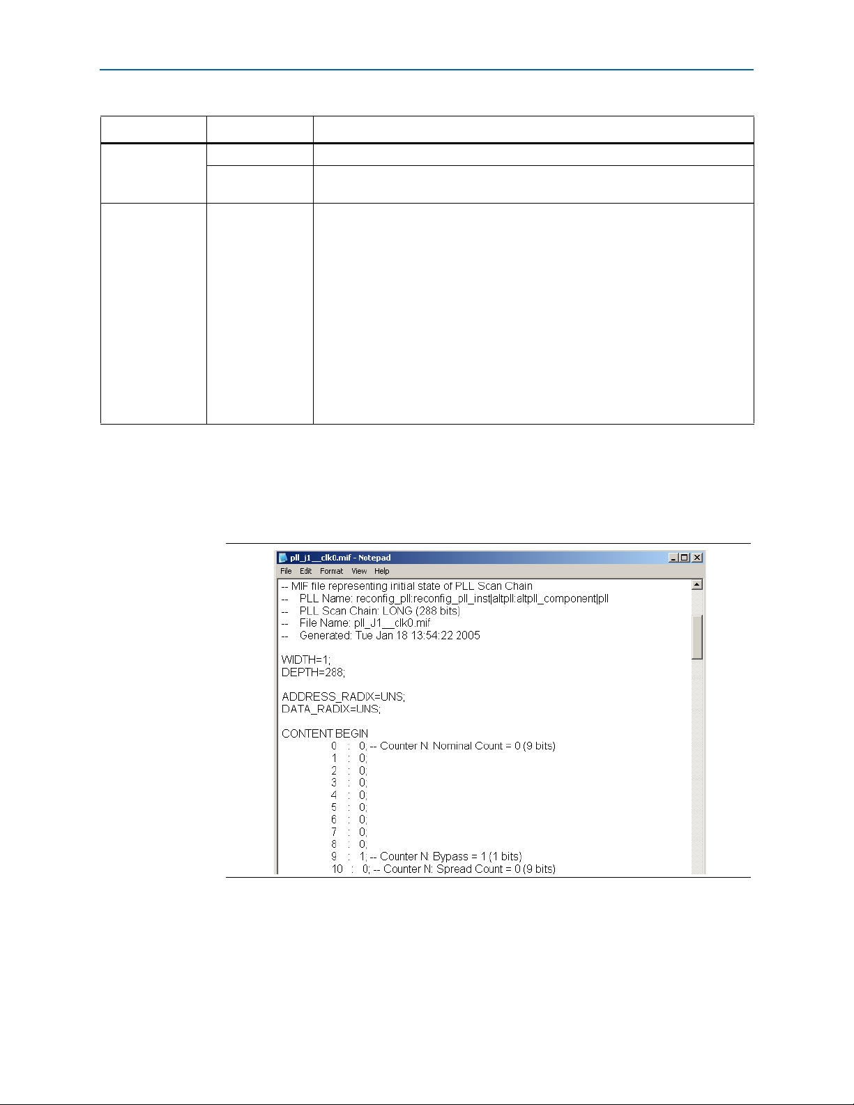
You c a n op e n a .mif in a text editor to make use of the comments embedded within
the file. These comments show you the scan chain values and positions based on your
design parameterization (see Figure 1). If you open a .mif in the Quartus II software,
you can regenerate the .mif in the ALTPLL parameter editor to restore the comments.
Figure 1. MIF file
f For more information about implementing PLL reconfiguration in the supported
Stratix series, refer to AN 282: Implementing PLL Reconfiguration in Stratix & Stratix GX
Devices, AN 367: Implementing PLL Reconfiguration in Stratix II Devices and AN 454:
Implementing PLL Reconfiguration in Stratix III Devices.
Phase-Locked Loop Reconfiguration (ALTPLL_RECONFIG) Megafunction February 2012 Altera Corporation
Page 5
Checking Design Violations With the Design Assistant Page 5
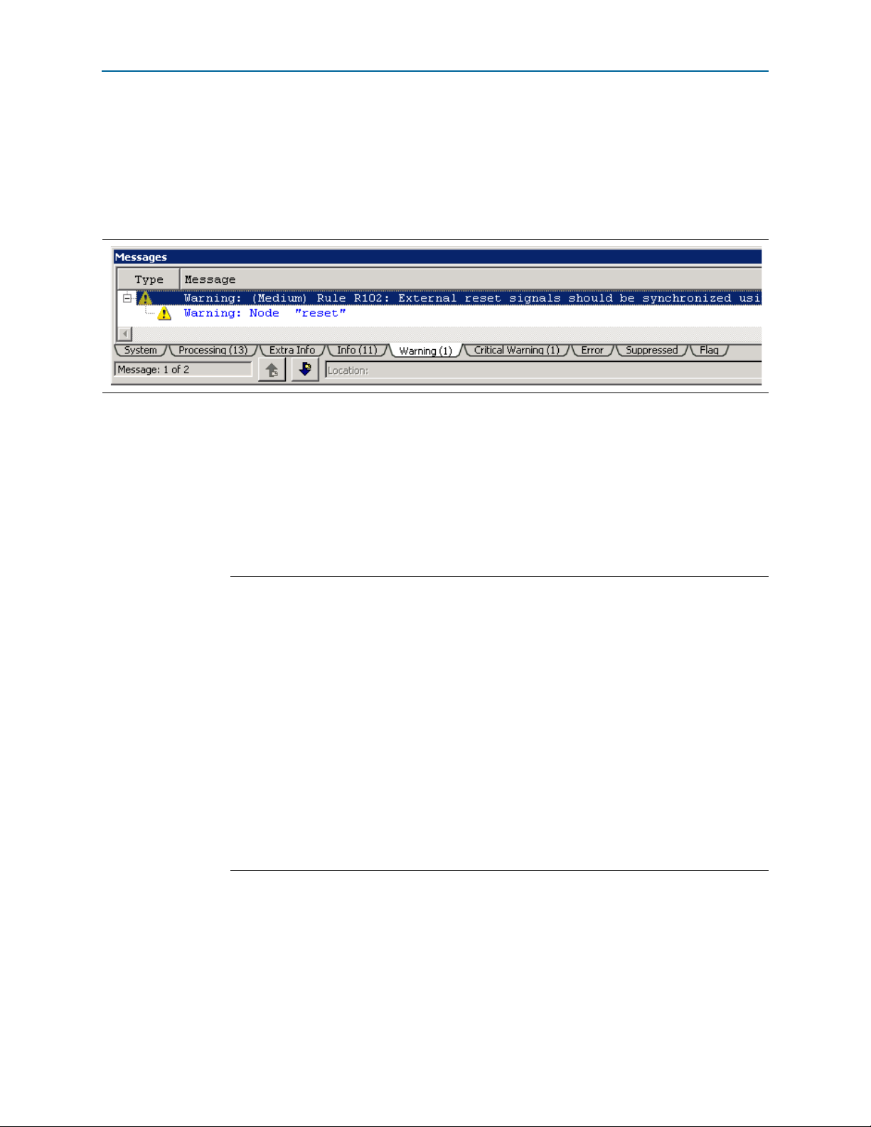
Checking Design Violations With the Design Assistant
The Design Assistant is a design rule checking tool that allows you to check for design
issues early in the design flow. When you run the Design Assistant in the Quartus II
software for the ALTPLL_RECONFIG megafunction, you might receive the warning
message shown in Figure 2.
Figure 2. Warning Message in Design Assistant
This message appears because there is a combinational logic in the megafunction that
connects the synchronous signal to the asynchronous external reset signal. To fix the
issue, you must synchronize the external reset signal outside the megafunction.
To synchronize the external reset signal, use the sample Verilog HDL code shown in
Example 1. In the example, the input of
reset pin, and the output of
sync_reset_dffe2
sync_reset_dffe1
is connected to the
is connected to the external
reset
input port of
the ALTPLL_RECONFIG megafunction.
Example 1. Code to Synchronize External Reset Signal
module synch_reg (reset, reconfig_clk, sync_reset_dffe2);
input reset, reconfig_clk;
output sync_reset_dffe2;
reg sync_reset_dffe1, sync_reset_dffe2;
always @(posedge reconfig_clk)
begin
sync_reset_dffe1 = reset;
end
always @(posedge reconfig_clk)
begin
sync_reset_dffe2 = sync_reset_dffe1;
end
endmodule
Phase-Locked Loop Reconfiguration (ALTPLL_RECONFIG) MegafunctionFebruary 2012 Altera Corporation
Page 6

Page 6 Simulation
Simulation
You can perform functional and gate-level timing simulations of the megafunction.
f For more information, refer to the appropriate chapter in the Simulation section in
volume 3 of the Quartus II Handbook.
If phase-shifting occurs after a PLL reconfiguration, use gate-level timing simulation
instead of functional simulation to verify the correct counter settings and phase shifts.
For non-zero PLL phase shifts, the frequency of the output clocks after a
reconfiguration is correct, but the phase may be incorrect. If the phase shift is
significant, use gate-level timing simulation to verify the timing behavior.
Functional Description—Implementing Multiple Reconfiguration Using an External ROM
The ALTPLL_RECONFIG megafunction allows you to reconfigure the PLL using an
external ROM with multiple configuration files. With this feature, you can perform
the following:
■ Specify an external ROM and feed its content to the ALTPLL_RECONFIG
megafunction.
■ Use the megafunction with multiple PLL configuration settings that are stored in
configuration files during user mode.
■ Use the megafunction with applications that require flexible dynamic-shifting of
PLL settings during user mode.
■ Reconfigure the initial PLL settings from a source other than an embedded
random-access memory (RAM), such as an off-chip flash device, which is useful in
HardCopy-type applications.
1 This feature is available for Stratix III, Stratix IV, Cyclone III, Cyclone IV,
HardCopy III, HardCopy IV, and Arria II GX devices only.
To support reconfiguration from multiple configuration files, the
ALTPLL_RECONFIG megafunction has three input ports and two output ports:
■ The
write_from_rom
input port signals the ALTPLL_RECONFIG megafunction
instantiation to write to the scan cache from the ROM.
■ The
■ The
rom_data_in
input port holds data from the ROM.
reset_rom_address
input port lets you restart the read process from the ROM.
The data arrives serially from the ROM, starting from bit 0.
■ The
rom_address_out
output bus holds the current address of the ROM data to be
written to the scan cache.
■ The
Phase-Locked Loop Reconfiguration (ALTPLL_RECONFIG) Megafunction February 2012 Altera Corporation
write_rom_ena
output port enables the intended ROM to be read out.
Page 7
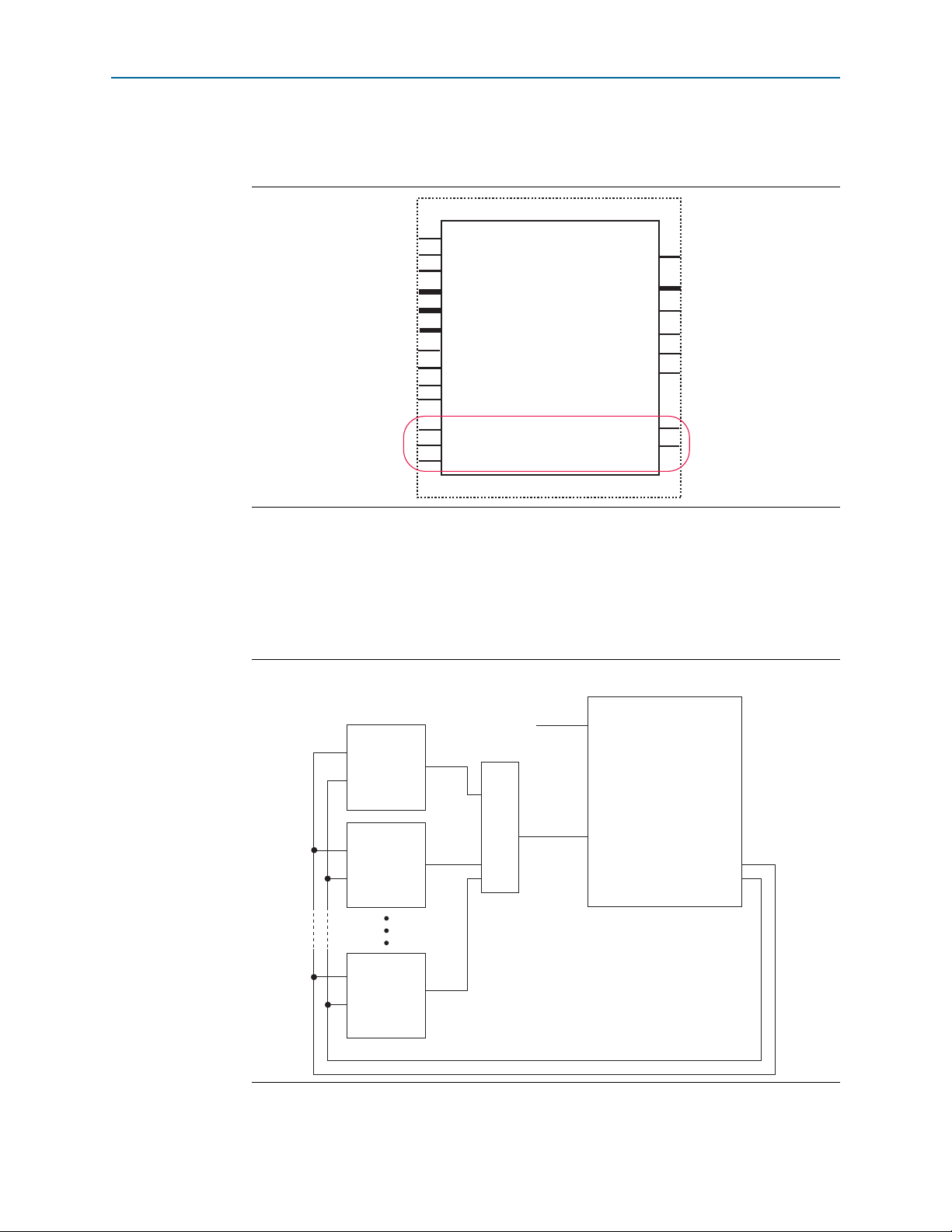
Functional Description—Implementing Multiple Reconfiguration Using an External ROM Page 7
The input and output ports to support reconfiguration using multiple configuration
files are shown in Figure 3, circled in red.
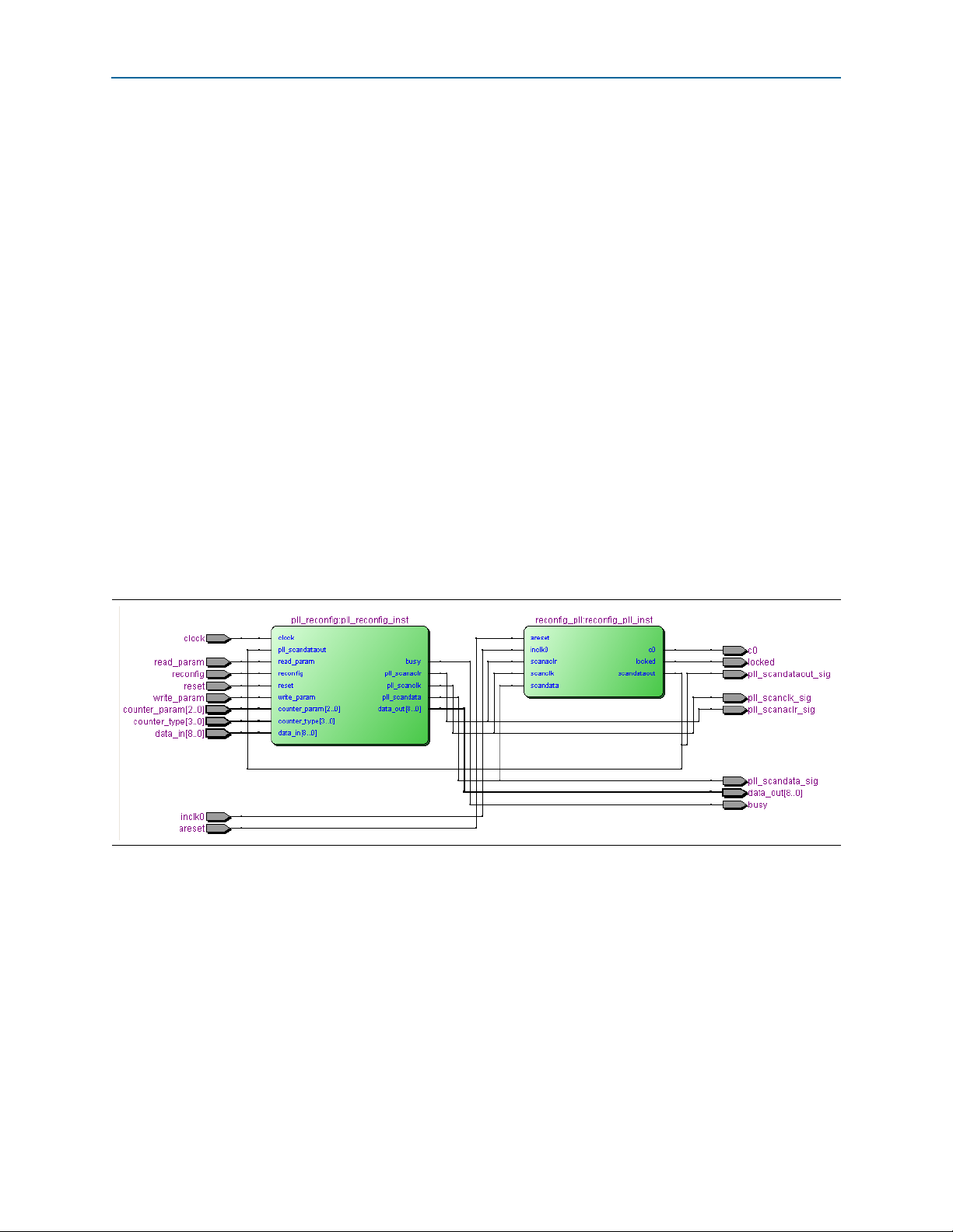
Figure 3. Ports to Support Reconfiguration Using Multiple Configuration Files
ALTPLL_RECONFIG
reconfig
read_param
write_param
data_in[8:0]
counter_type[3:0]
counter_param[2:0]
pll_scandataout
clock
reset
pll_areset_in
busy
data_out[8:0]
pll_scanclk
pll_scandata
pll_scanaclr
pll_areset
write_from_rom
rom_data_in
reset_rom_address
inst
rom_address_out
write_rom_ena
The reconfiguration feature using multiple configuration files allows you to feed data
from multiple ROMs to a multiplexer that feeds the
a sample design. In this scheme, the
write_rom_ena
rom_data_in
signal feeds back to the ROM as
the enable signal, which allows the ROM to be read out. The
port. Figure 4 shows
rom_address_out
bus
provides the intended ROM address, which determines the exact ROM data.
Figure 4. Typical Scheme for Reconfiguring PLLs from External ROMs
write_from_rom
ROM
altpll_reconfig
M
U
X
ROM
rom_data_in
write_rom_ena
rom_address_out
ROM
Phase-Locked Loop Reconfiguration (ALTPLL_RECONFIG) MegafunctionFebruary 2012 Altera Corporation
Page 8
Page 8 Functional Description—Implementing Multiple Reconfiguration Using an External ROM
To copy the data from a ROM to the ALTPLL_RECONFIG megafunction scan cache (a
memory location that stores the PLL reconfiguration settings), you must hold the
write_from_rom
signal on the first rising edge of the clock after the
signal high for 1 clock cycle. The megafunction asserts the busy
write_from_rom
signal goes high.
The busy signal remains asserted until all the bits are written into the scan cache.
On the second rising edge of the clock after the
write_from_rom
signal goes low
again, the intended ROM address for the write operation appears on the
rom_address_out
rom_address_out
megafunction instantiation. The
rising edge of the clock after the
port. The data of the ROM specified by the intended address on
is fed to the rom_
data_in
input port of the ALTPLL_RECONFIG
write_rom_ena
write_from_rom
signal is also asserted on the second
signal goes low again (refer to
Figure 5).
Figure 5. Beginning Write to the Scan Cache of the ALTPLL_RECONFIG Megafunction from the ROM
The writing-to-scan cache process continues until the address reaches the specific size
of the scan cache (234 for Stratix III device top and bottom PLL, 180 for Stratix III
device left and right PLL, and 144 for Cyclone III PLL). This process is completed
when the
busy
signal is deasserted. This means that the scan cache of the
ALTPLL_RECONFIG megafunction is written with the intended reconfiguration
settings from the ROM.
Phase-Locked Loop Reconfiguration (ALTPLL_RECONFIG) Megafunction February 2012 Altera Corporation
Page 9
Functional Description—Implementing Multiple Reconfiguration Using an External ROM Page 9
After this, the
reconfig
signal can be asserted for 1 clock cycle to reconfigure the PLL
to the intended settings that have been written to the scan cache of the
ALTPLL_RECONFIG megafunction (refer to Figure 6).
Figure 6. Completing Write to the Scan Cache of the ALTPLL_RECONFIG Megafunction from the ROM
Note to Figure 6:
(1) This figure also shows the beginning of the reconfiguration process.
If you assert the
1 clock cycle and the
asserted, the write process then restarts from address
reset_rom_address
rom_address_out
signal, the
write_rom_ena
signal resets. When the
0
(refer to Figure 7).
signal is deasserted for
write_rom_ena
(1)
gets
Figure 7. Asserting the reset_rom_address Signal
Phase-Locked Loop Reconfiguration (ALTPLL_RECONFIG) MegafunctionFebruary 2012 Altera Corporation
Page 10

Page 10 Design Example
Design Example
You can download design examples for this megafunction from the following
locations:
■ On the Documentation: Quartus II Development Software page, in the Using
Megafunctions section under I/O
■ On the Documentation: User Guides webpage, with this user guide
The designs are simulated using the ModelSim
waveform display of the device behavior. For more information about the ModelSimAltera software, refer to the ModelSim-Altera Software Support page on the Altera
website. The support page includes links to such topics as installation, usage, and
troubleshooting.
Frequency Division
This design example uses the ALTPLL_RECONFIG megafunction to change the clock
frequency of an enhanced PLL. This example demonstrates how to reconfigure the
counter using the ALTPLL_RECONFIG megafunction to vary the frequency of this
counter by changing the c value. Figure 8 shows the formula for changing the c value
for different PLL output frequencies.
®
-Altera software to generate a
c0
Figure 8. Frequency Division Formula
Divide-by value = c = (Fin * m)/(Fout * n)
Where:
c value = High time count = Low time count
Fin = Input frequency
m = m modulus value
n = n modulus value
Fout = Required output frequency
This example reconfigures the output frequency of
c0
from 100to50MHz by
changing the divide-by value from 3 to 6.
Generating the ALTPLL and ALTPLL_RECONFIG Megafunctions
To generate the ALTPLL and ALTPLL_RECONFIG megafunctions, follow these steps:
1. Open the altpll_reconfig_DesignExample_ex1.zip file and extract
pll_recon_ex1_1.1.qar.
2. In the Quartus II software, open the pll_recon_ex1_1.1.qar file and restore the
archive file into your working directory.
3. On the Tools menu, click MegaWizard Plug-In Manager. Page 1 of the
MegaWizard Plug-In Manager appears.
4. Select Create a new custom megafunction variation.
5. Click Next. Page 2a of the MegaWizard Plug-In Manager appears.
Phase-Locked Loop Reconfiguration (ALTPLL_RECONFIG) Megafunction February 2012 Altera Corporation
Page 11

Design Example Page 11
6. In the MegaWizard Plug-In Manager pages, select or verify the configuration
settings listed in Tab le 2. Click Next to advance from one page to the next.
Table 2. Configuration Settings for the ALTPLL Megafunction (Part 1 of 2)
MegaWizard Plug-In
Manager Page
2a
Parameter Settings
(General/Modes)
Parameter Settings
(Scan/Inputs/Lock)
Output Clocks
(clk c0)
EDA Generate netlist Turned off
Settings Value
Megafunction Under the I/O category, select ALTPLL
Which device family will you be using? Stratix
Which type of output file do you want to
create?
VHDL
What name do you want for the output file? reconfig_pll
Return to this page for another create
operation
Turned on
Currently selected device family Stratix
Match project/default Turned on
Which device speed grade will you be
using?
Any
What is the frequency of inclk0 input 100 MHz
Which PLL type will you be using? Enhanced PLL
How will the PLL outputs be generated?
Which output clock will be compensated
for?
Create optional inputs for dynamic
reconfiguration
Long chain: All 6 core and 4 external clocks
are available
Create an ‘pllena’ input to selectively enable
the PLL
Create an ‘areset’ input to asynchronously
reset the PLL
Create an ‘pfdena’ input to selectively
enable the phase/frequency detector
Select Use the feedback path inside the PLL.
Select In normal mode
c0
Turned on
Selected
Turned off
Turned on
Turned off
Create ‘locked’ output Turned on
Create output file(s) using ‘Advanced’ PLL
parameters
Turned off
Use this clock Turned on
Enter output clock frequency 100 MHz
Clock phase shift 0 degrees
Clock duty cycle (%) 50
Create a clock enable input Turned off
Phase-Locked Loop Reconfiguration (ALTPLL_RECONFIG) MegafunctionFebruary 2012 Altera Corporation
Page 12
Page 12 Design Example
Table 2. Configuration Settings for the ALTPLL Megafunction (Part 2 of 2)
MegaWizard Plug-In
Manager Page
Summary
Variation file Turned on
PinPlanner ports PPF file Turned on
AHDL Include file Turned on
VHDL component declaration file Turned on
Quartus II symbol file Turned on
Instantiation template file Turned on
7. Click Finish. The
Settings Value
reconfig_pll
module is built.
8. Click OK. The MegaWizard Plug-In Manager resets to page 2a to allow you to
create a new custom megafunction variation.
9. In the MegaWizard Plug-In Manager pages, select or verify the configuration
settings listed in Tab le 3. Click Next to advance from one page to the next.
Table 3. Configuration Settings for the ALTPLL_RECONFIG Megafunction
MegaWizard Plug-In
Manager Page
2a
Parameter Settings
(General)
Parameter Settings
(General 2)
EDA Generate netlist Turned off
Summary
Megafunction
Which device family will you be using? Stratix
Which type of output file do you want to
create?
What name do you want for the output file? pll_reconfig
Return to this page for another create
operation
Currently selected device family Stratix
Match project/default Turned on
Which scan chain type will you be using Long chain
Do you want to specify initial value of the
scan chain?
File name pll_j1__clk0.mif
Do not use pre initialized RAM - initialize
from ROM instead
Variation file Turned on
AHDL Include file Turned on
VHDL component declaration file Turned on
Quartus II symbol file Turned on
Instantiation template file Turned on
Settings Value
Under the I/O category, select
ALTPLL_RECONFIG
VHDL
Turned off
Select Yes, use this file for the content data
Turned off
10. Click Finish. The
Phase-Locked Loop Reconfiguration (ALTPLL_RECONFIG) Megafunction February 2012 Altera Corporation
pll_reconfig
module is built.
Page 13
Design Example Page 13
Compiling the ALTPLL and ALTPLL_RECONFIG Megafunctions
To add the ALTPLL megafunction to the ALTPLL_RECONFIG megafunction, and
then compile the design in the Quartus II software, follow these steps:
1. On the Project menu, click Add/Remove File in Project. The Settings dialog box
appears.
2. In the Category list, select Files.
3. Click Browse (...) after File name and select pll_recon_ex1.vhd from the project
folder. This file is the top-level module that contains the port-mapping between
the
pll_reconfig
4. Click Add to add the top-level file to the project.
5. Click OK.
6. On the File menu, click Save Project.
The top-level file is added to the project.
7. To compile the design, on the Processing menu, click Start Compilation.
8. When the Full Compilation was successful message box appears, click OK.
and
reconfig_pll
instances.
You have now created and compiled the complete design file, which can be viewed in
the RTL Viewer (Figure 9). To display the RTL Viewer, in the Tools menu, select
Netlist Viewers, and click on RTL Viewer.
Figure 9. RTL Viewer — Complete Design File
Simulating the Design Example
To simulate the design example using the ModelSim-Altera software, follow these
steps:
1. Unzip the altpll_reconfig_ex1_msim.zip file to any working directory on your
PC.
2. Browse to the folder in which you unzipped the files.
3. Open remote_update_ex2.do in a text editor.
4. In line 1 of the altpll_reconfig_ex1_msim.do file, ensure that the directory path of
the library files is correct. For example, C:/Modeltech_ae/altera/verilog/stratix.
5. On the File menu, click Save.
Phase-Locked Loop Reconfiguration (ALTPLL_RECONFIG) MegafunctionFebruary 2012 Altera Corporation
Page 14
Page 14 Design Example
6. Launch the ModelSim-Altera software.
7. On the File menu, click Change Directory.
8. Select the folder in which you unzipped the files.
9. Click OK.
10. On the Tools menu, click Execute Macro.
11. Select the altpll_reconfig_ex1_msim.do file and click Open. This is a script file for
ModelSim-Altera software to automate all the necessary settings for the
simulation.
12. Verify the results shown in the Wave window.
You can rearrange, remove, and add signals, and change the radix by modifying the
script altpll_reconfig_ex1_msim.do.
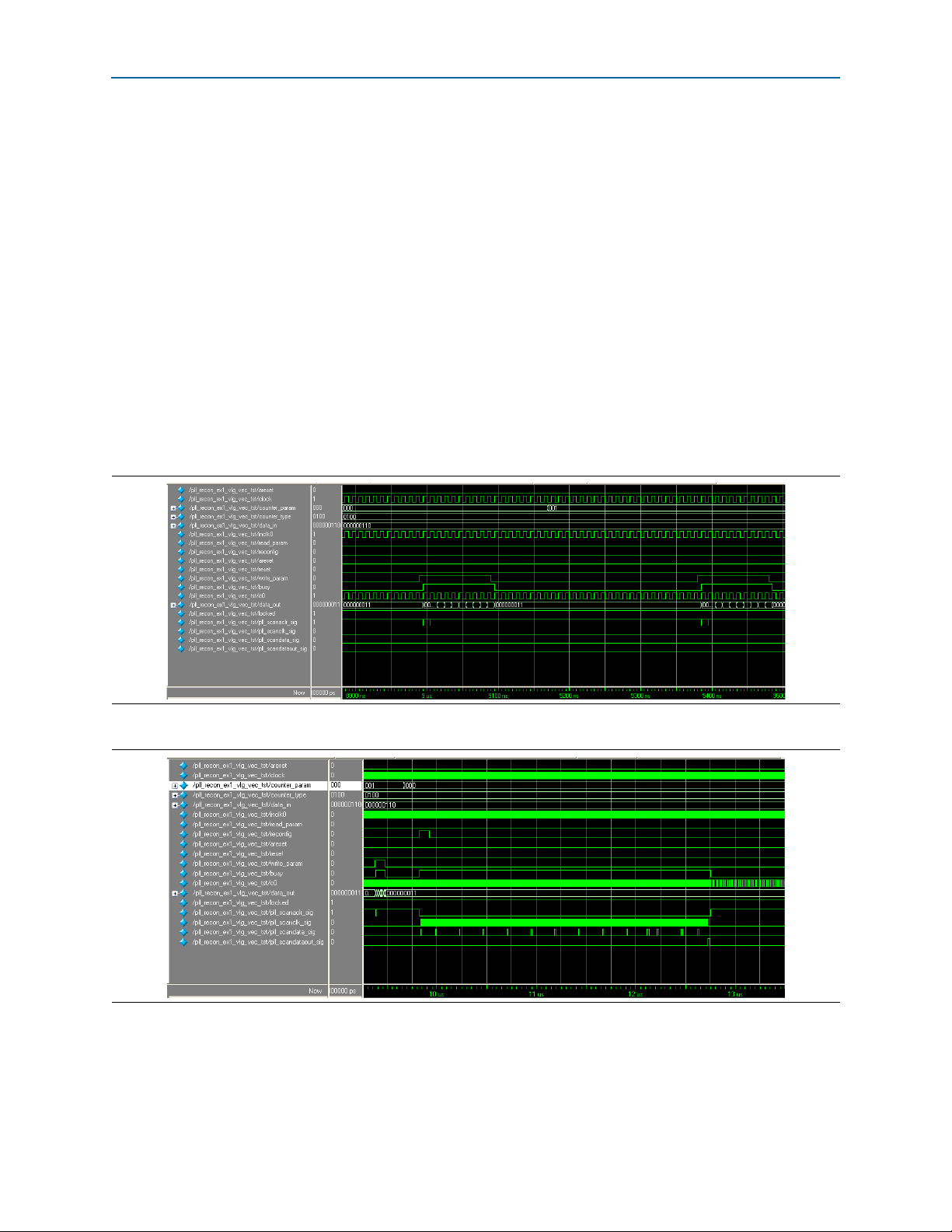
Figure 10 and Figure 11 show the expected simulation results in the ModelSim-Altera
software. Figure 11 shows the change in
Figure 10. Simulation Results in the ModelSim-Altera Software (8.9 to 9.5 ms)
c0
frequency starting from 12.75 ms.
Figure 11. Simulation Results in the ModelSim-Altera Software (9.5 to 13.5 ms)
Phase-Locked Loop Reconfiguration (ALTPLL_RECONFIG) Megafunction February 2012 Altera Corporation
Page 15

Design Example Page 15
Duty cycle = (Ch/Ct) % high time count and (Cl/Ct) % low time count
with RSELODD = 0
Where:
Ch = High time count
Cl = Low time count
Ct = Total time
When you set RSELODD = 1, you subtract 0.5 cycles from the high time and
you add 0.5 cycles to the low time.
For example, if:
Ch = 2 cycles
Cl = 1 cycle
(Note: For odd division factors, the larger number is for the
Ch counter; the smaller number is for the CI counter.)
Setting RSELODD = 1 effectively changes the Ch and Cl to:
High time count = 1.5 cycles
Low time count = 1.5 cycles
Duty cycle = (1.5/3) % high time count and (1.5/3) % low time count
Pulse Width Variation
This design example uses the ALTPLL_RECONFIG megafunction to modify the pulse
width of an enhanced PLL. This example demonstrates how to reconfigure the
counter using the ALTPLL_RECONFIG megafunction to vary the pulse width of this
counter by changing the high-count and low-count values. The formula for changing
the duty cycle is shown in Figure 12.
Figure 12. Changing the Duty Cycle Formula
c1
In this example, the pulse width is programmed to change from 50% to 25% , and then
to 75% of the duty cycle.
Generating the ALTPLL and ALTPLL_RECONFIG Megafunctions
To generate the ALTPLL and ALTPLL_RECONFIG megafunctions, perform the
following steps:
1. Open ALTPLL_RECONFIG_DesignExample_ex2.zip and extract
pll_recon_ex2_1.1.qar.
2. In the Quartus II software, open pll_recon_ex2_1.1.qar and restore the archive file
into your working directory.
3. On the Tools menu, click MegaWizard Plug-In Manager. Page 1 of the
MegaWizard Plug-In Manager appears.
4. Select Create a new custom megafunction variation.
5. Click Next. Page 2a of the MegaWizard Plug-In Manager appears.
Phase-Locked Loop Reconfiguration (ALTPLL_RECONFIG) MegafunctionFebruary 2012 Altera Corporation
Page 16

Page 16 Design Example
6. In the MegaWizard Plug-In Manager pages, select or verify the configuration
settings listed in Tab le 4. Click Next to advance from one page to the next.
Table 4. Configuration Settings for the ALTPLL Megafunction (Part 1 of 2)
MegaWizard
Plug-In Manager
Settings Value
Page
Megafunction Under the I/O category, select ALTPLL
Which device family will you be using? Stratix
2a
Which type of output file do you want to
create?
VHDL
What name do you want for the output file? reconfig_pll
Return to this page for another create
operation
Tur n e d o n
Currently selected device family Stratix
Match project/default Turned on
Parameter Settings
(General/Modes)
Parameter Settings
(Scan/Inputs/Lock)
Which device speed grade will you be
using?
What is the frequency of inclk0 input 20 MHz
Which PLL type will you be using? Enhanced PLL
How will the PLL outputs be generated?
Which output clock will be compensated
for?
Create optional inputs for dynamic
reconfiguration
Long chain: All 6 core and 4 external clocks
are available
Create an ‘pllena’ input to selectively enable
the PLL
Create an ‘areset’ input to asynchronously
reset the PLL
Create an ‘pfdena’ input to selectively
enable the phase/frequency detector
Any
Select Use the feedback path inside the PLL.
Select In normal mode
c1
Tur n e d o n
Selected
Tur n e d o f f
Tur n e d o n
Tur n e d o f f
Create ‘locked’ output Turned on
Create output file(s) using ‘Advanced’ PLL
parameters
Tur n e d o f f
Use this clock Turned on
Output Clocks
(clk c1)
Enter output clock frequency 15 MHz
Clock phase shift 0 degrees
Clock duty cycle (%) 50
Create a clock enable input Turned off
EDA Generate netlist Turned off
Phase-Locked Loop Reconfiguration (ALTPLL_RECONFIG) Megafunction February 2012 Altera Corporation
Page 17

Design Example Page 17
Table 4. Configuration Settings for the ALTPLL Megafunction (Part 2 of 2)
MegaWizard
Plug-In Manager
Page
Summary
Variation file Turned on
PinPlanner ports PPF file Turned on
AHDL Include file Turned on
VHDL component declaration file Turned on
Quartus II symbol file Turned on
Instantiation template file Turned on
Settings Value
7. Click Finish. The
reconfig_pll
module is built.
8. Click OK. The MegaWizard Plug-In Manager resets to page 2a to allow you to
create a new custom megafunction variation.
9. In the MegaWizard Plug-In Manager pages, select or verify the configuration
settings listed in Tab le 5. Click Next to advance from one page to the next.
Table 5. Configuration Settings for the ALTPLL_RECONFIG Megafunction
MegaWizard
Plug-In Manager
Page
Megafunction Under the I/O category, select ALTPLL_RECONFIG
Which device family will you be using? Stratix
Which type of output file do you want to
2a
Parameter Settings
(General)
Parameter Settings
(General)
EDA Generate netlist Turned off
Summary
create?
What name do you want for the output file? pll_reconfig
Return to this page for another create
operation
Currently selected device family Stratix
Match project/default Turned on
Which scan chain type will you be using Long chain
Do you want to specify initial value of the
scan chain?
File name pll_j1__pll.mif
Do not use pre initialized RAM - initialize
from ROM instead
Variation file Turned on
AHDL Include file Turned on
VHDL component declaration file Turned on
Quartus II symbol file Turned on
Instantiation template file Turned on
Settings Value
VHDL
Turned off
Select Yes, use this file for the content data
Turned off
10. Click Finish. The
pll_reconfig
module is built.
Phase-Locked Loop Reconfiguration (ALTPLL_RECONFIG) MegafunctionFebruary 2012 Altera Corporation
Page 18

Page 18 Design Example
Compiling the ALTPLL and ALTPLL_RECONFIG Megafunctions
To add the ALTPLL megafunction to the ALTPLL_RECONFIG megafunction, and
then compile the design in the Quartus II software, follow these steps:
1. On the Project menu, click Add/Remove Files in Project. The Settings dialog box
appears.
2. In the Category list, select Files.
3. Click Browse (...) after File name and from the project folder, select
pll_recon_ex2.vhd. This file is the top-level module that contains the
port-mapping between the
4. To add the top-level file to the project, click Add.
5. Click OK.
6. On the File menu, click Save Project.
The top-level file is added to the project.
7. To compile the design, on the Processing menu, click Start Compilation.
8. When the Full Compilation was successful message box appears, click OK.
pll_reconfig
and
reconfig_pll
instances.
You have now created and compiled the complete design file, which can be viewed in
the RTL Viewer (Figure 13). To display the RTL Viewer, in the Tools menu, select
Netlist Viewers, and click on RTL Viewer.
Figure 13. RTL Viewer — Complete Design File
Phase-Locked Loop Reconfiguration (ALTPLL_RECONFIG) Megafunction February 2012 Altera Corporation
Page 19

Design Example Page 19
Simulating the Design Example
To simulate the design example using the ModelSim-Altera software, follow these
steps:
1. Unzip the altpll_reconfig_ex2_msim.zip file to any working directory on your
PC.
2. Browse to the folder in which you unzipped the files.
3. Open the remote_update_ex2.do file in a text editor.
4. In line 1 of the altpll_reconfig_ex2_msim.do file, make sure the directory path of
the library files is correct. For example, C:/Modeltech_ae/altera/verilog/stratix.
5. On the File menu, click Save.
6. Launch the ModelSim-Altera software.
7. On the File menu, click Change Directory.
8. Select the folder in which you unzipped the files.
9. Click OK.
10. On the Tools menu, click Execute Macro.
11. Select the altpll_reconfig_ex2_msim.do file and click Open. This is a script file for
ModelSim-Altera software to automate all of the necessary settings for the
simulation.
12. Verify the results shown in the Wave window.
You can rearrange, remove, and add signals. and change the radix by modifying the
script altpll_reconfig_ex2_msim.do.
Figure 14 through Figure 19 show the expected simulation results in the
ModelSim-Altera software. The duty cycle changes from a ratio of 50:50 to 25:75 and
finally to 75:25.
Figure 14. Changing Parameters (2.11 to 7.23 ms)
Phase-Locked Loop Reconfiguration (ALTPLL_RECONFIG) MegafunctionFebruary 2012 Altera Corporation
Page 20

Page 20 Design Example
Figure 15. Reconfiguration (6.32 to 26.8 ms)
Figure 16. Pulse Width Changes From 50:50 Ratio to 25:75 Ratio (20 to 26 ms)
Phase-Locked Loop Reconfiguration (ALTPLL_RECONFIG) Megafunction February 2012 Altera Corporation
Page 21

Design Example Page 21
Figure 17. Changing Parameters (91.79 to 96.91 ms)
Figure 18. Reconfiguration (96.92 to 117.4 ms)
Phase-Locked Loop Reconfiguration (ALTPLL_RECONFIG) MegafunctionFebruary 2012 Altera Corporation
Page 22

Page 22 Design Example
Figure 19. Pulse Width Changes To 75:25 Ratio (110 to 113 ms)
Phase-Locked Loop Reconfiguration (ALTPLL_RECONFIG) Megafunction February 2012 Altera Corporation
Page 23

Design Example Page 23
PLL Reconfiguration with Multiple .mif Files
This design example uses the ALTPLL_RECONFIG megafunction to reconfigure the
output of the
external ROMs in Stratix III devices. The .mif files specify PLL settings that
reconfigure the output of the
and 500 MHz, then back to 200 MHz.
Generating the ALTPLL and ALTPLL_RECONFIG Megafunctions
To generate the ALTPLL and ALTPLL_RECONFIG megafunctions, follow these steps:
1. Open the ALTPLL_RECONFIG_DesignExample_ex3.zip file to any directory on
your PC.
2. Open the ALTPLL_RECONFIG_rom.qar project file.
3. On the Tools menu, click MegaWizard Plug-In Manager. Page 1 of the
MegaWizard Plug-In Manager appears.
4. Select the Create a new custom megafunction variation option.
5. Click Next. Page 2a of the MegaWizard Plug-In Manager appears.
c0
counter based on the PLL settings specified in multiple .mif files from
c0
counter from 100 to 200 MHz, 300 MHz, 400 MHz,
6. In the MegaWizard Plug-In Manager pages, select or verify the configuration
settings listed in Tab le 6. Click Next to advance from one page to the next.
Table 6. Configuration Settings for the ALTPLL Megafunction (Part 1 of 2)
MegaWizard Plug-In
Manager Page
2a
Parameter Settings
(General/Modes)
Megafunction Under the I/O category, select ALTPLL
Which device family will you be using? Stratix III
Which type of output file do you want to
create?
What name do you want for the output file? the_pll.v
Return to this page for another create
operation
Currently selected device family Stratix III
Match project/default Turned on
Which device speed grade will you be
using?
What is the frequency of inclk0 input 50 MHz
Which PLL type will you be using? Top_Bottom PLL
How will the PLL outputs be generated?
Which output clock will be compensated
for?
Settings Value
Verilog
Turned on
Any
Select Use the feedback path inside the PLL.
Select In normal mode
c0
Phase-Locked Loop Reconfiguration (ALTPLL_RECONFIG) MegafunctionFebruary 2012 Altera Corporation
Page 24

Page 24 Design Example
Table 6. Configuration Settings for the ALTPLL Megafunction (Part 2 of 2)
MegaWizard Plug-In
Manager Page
Parameter Settings
(Scan/Inputs/Lock)
PLL Reconfiguration
Output Clocks
(clk c0)
EDA Generate netlist Turned off
Summary
Settings Value
Create an ‘pllena’ input to selectively enable
the PLL
Create an ‘areset’ input to asynchronously
reset the PLL
Create an ‘pfdena’ input to selectively
enable the phase/frequency detector
Disabled
Turned on
Turned off
Create ‘locked’ output Turned on
Enable self reset on loss lock Turned off
Create output file(s) using ‘Advanced’ PLL
parameters
Create optional inputs for dynamic
reconfiguration
Turned off
Turned on
the_pll_initial.mif—taking an
50 MHz and generating
Initial Configuration File (filename)
Ensure that this option shows the correct path of
the .mif file before compiling the design to avoid
scan chain mismatch warnings.
The files are already generated. They are:
■ the_pll_200_mhz.mif—taking an
50 MHz and generating
■ the_pll_300_mhz.mif—taking an
Additional Configuration File (filename)
50 MHz and generating c0 of 300 MHz
■ the_pll_400_mhz.mif—taking an
50 MHz and generating
■ the_pll_500_mhz.mif—taking an
50 MHz and generating
Create optional inputs for dynamic phase
reconfiguration
Turned off
Use this clock Turned on
Enter output clock frequency 100 MHz
Clock phase shift 0 degrees
Clock duty cycle (%) 50
Variation file Turned on
PinPlanner ports PPF file Turned on
AHDL Include file Turned on
VHDL component declaration file Turned on
Quartus II symbol file Turned on
Instantiation template file Turned on
Verilog HDL block box file Turned on
Reconfiguration File for altpll_reconfig Turned on
inclock
c0
of 100 MHz
c0
of 200 MHz
c0
of 400 MHz
c0
of 500 MHz
of
inclock
inclock
inclock
inclock
of
of
of
of
Phase-Locked Loop Reconfiguration (ALTPLL_RECONFIG) Megafunction February 2012 Altera Corporation
Page 25

Design Example Page 25
The ALTPLL megafunction allows you to generate additional configuration files
without going through a compilation stage. It allows you to generate as many
unique configuration files as you need without the difficulty of multiple
compilation flows. All you need to do is to set the intended PLL settings, enter the
file name, and click Generate A Configuration File. Use this capability with the
PLL reconfiguration of multiple .mif files via external ROMs in the
ALTPLL_RECONFIG megafunction.
7. Click Finish. The the_pll.v module is built.
8. Click OK. The MegaWizard Plug-In Manager resets to page 2a so you can create a
new custom function variation.
9. In the MegaWizard Plug-In Manager pages, select or verify the configuration
settings listed in Tab le 7. Click Next to advance from one page to the next.
Table 7. Configuration Settings for the ALTPLL_RECONFIG Megafunction
MegaWizard
Plug-In
Manager Page
Megafunction Under the I/O category, select ALTPLL_RECONFIG
Which device family will you be using? Stratix III
Which type of output file do you want to
2a
Parameter
Settings
(General)
Parameter
Settings
(General)
EDA Generate netlist Turned off
Summary
create?
What name do you want for the output file? pll_reconfig_circuit.v
Return to this page for another create
operation
Currently selected device family Stratix III
Match project/default Turned on
Which scan chain type will you be using Top/Bottom
Do you want to specify initial value of the
scan chain?
File name
Do not use pre initialized RAM - initialize
from ROM instead
Add ports to write to the scan chain from
external ROM during run time
Variation file Turned on
AHDL Include file Turned on
VHDL component declaration file Turned on
Quartus II symbol file Turned on
Instantiation template file Turned on
Verilog HDL block-box file Turned on
Settings Value
Verilog
Turned off
Select Yes, use this file for the content data
the_pll_initial_mif.mif
Ensure that this option shows the correct path of the .mif
file before compiling the design to avoid scan chain
mismatch warnings.
Turned off
Turned on
10. Click Finish. The
pll_reconfig_circuit
Phase-Locked Loop Reconfiguration (ALTPLL_RECONFIG) MegafunctionFebruary 2012 Altera Corporation
module is built.
Page 26

Page 26 Design Example
Compiling the ALTPLL and ALTPLL_RECONFIG Megafunctions
To add the ALTPLL megafunction to the ALTPLL_RECONFIG megafunction, and
then compile the design in the Quartus II software, follow these steps:
1. On the Project menu, click Add/Remove Files in Project. The Settings dialog box
appears.
2. In the Category list, select Files.
3. Click Browse (...) after File name and from the project folder, select
ALTPLL_RECONFIG_rom.v. This file is the top-level module that contains the
port-mapping between the
4. To add the top-level file to the project, click Add.
5. Click OK.
6. On the File menu, click Save Project.
The top-level file is added to the project.
7. To compile the design, on the Processing menu, click Start Compilation.
8. When the Full Compilation was successful message box appears, click OK.
pll_reconfig_circuit
and
the_pll
instances.
You have now created and compiled the complete design file, which can be viewed in
the RTL Viewer (Figure 20). To display the RTL Viewer, in the Tools menu, select
Netlist Viewers, and click on RTL Viewer.
Figure 20. Top-Level Design Implementation Using the RTL Viewer
This design consists of eight modules, which are:
1. the_pll:u1—This represents the Stratix III PLL (Top and Bottom PLL) that is to be
reconfigured. The settings are as follows:
■
inclk
= 50 MHz
■
c0
= 100 MHz
Phase-Locked Loop Reconfiguration (ALTPLL_RECONFIG) Megafunction February 2012 Altera Corporation
Page 27

Design Example Page 27
2. pll_reconfig_circuit:u2—This represents the PLL reconfiguration circuitry used
by the PLL to reconfigure its settings during user mode. In addition, this circuitry
has a scan-chain cache, which contains the intended PLL settings to be
reconfigured. It also has additional ports to take advantage of cycling multiple
.mif files for reconfiguration from external ROMs. This design example
demonstrates the capability of these ports. The settings are represented by the
the_pll_initial.mif file. The settings are as follows:
■
inclk
= 50 MHz
■
c0
= 100 MHz
3. rom_muxer:u3—This represents a 4-to-1 multiplexer used to multiplex serial data
coming from four ROMs to the
module. The multiplexer is used because the
rom_data_in
port of the pll_reconfig_circuit
rom_data_in
port is 1 bit in size;
however, it is controlled by a 2-bit selector, hence its ability to multiplex four
signals.
4. rom_1:u4—This represents the external ROM, which contains the intended
reconfiguration settings of the PLL. It has a 1-bit output port (
q
) because of the
serial nature of writing the intended PLL settings to the scan-chain cache of the
pll_reconfig_circuit module. It has a capacity of 256 words of 1-bit size. The ROM
uses 256 words because that is the closest approximate size of the scan-chain file
for this type of PLL, which is 234 bits. For this ROM, it is represented by the
the_pll_200_mhz.mif file, which is 234 bits. The settings are as follows:
■
inclk
= 50 MHz
■
c0
= 200 MHz
5. rom_2:u5—This represents the external ROM, which contains the intended
reconfiguration settings of the PLL. It has a 1-bit output port (
q
) because of the
serial nature of writing the intended PLL settings to the scan-chain cache of the
pll_reconfig_circuit module. It has a capacity of 256 words of 1-bit size. The ROM
uses 256 words because that is the closest approximate size of the scan-chain file
for this type of PLL, which is 234 bits. For this ROM, it is represented by the
the_pll_300_mhz.mif file, which is 234 bits. The settings are as follows:
■
inclk
= 50 MHz
■
c0
= 300 MHz
6. rom_3:u6—This represents the external ROM, which contains the intended
reconfiguration settings of the PLL. It has a 1-bit output port (
q
) because of the
serial nature of writing the intended PLL settings to the scan-chain cache of the
pll_reconfig_circuit module. It has a capacity of 256 words of 1-bit size. The ROM
uses 256 words because that is the closest approximate size of the scan-chain file
for this type of PLL, which is 234 bits. For this ROM, it is represented by the .mif
file the_pll_400_mhz.mif, which is 234 bits. The settings are as follows:
■
inclk
= 50 MHz
■
c0
= 400 MHz
Phase-Locked Loop Reconfiguration (ALTPLL_RECONFIG) MegafunctionFebruary 2012 Altera Corporation
Page 28

Page 28 Design Example
state_0
state_1
state_2
state_3 state_4
state_5
state_6
reset
7. rom_4:u7—This represents the external ROM, which contains the intended
reconfiguration settings of the PLL. It is has a 1-bit output port (
q
) because of the
serial nature of writing the intended PLL settings to the scan-chain cache of the
pll_reconfig_circuit module. It has a capacity of 256 words of 1-bit size. The ROM
uses 256 words because that is the closest approximate size of the scan-chain file
for this type of PLL, which is 234 bits. For this ROM, it is represented by the .mif
file the_pll_500_mhz.mif, which is 234 bits. The settings are as follows:
■
inclk
= 50 MHz
■
c0
= 500 MHz
8. control_sm:u8—This represents the state machine that controls the three main
processes involved in the PLL reconfiguration with multiple .mif files via external
ROMs. The state machine selects the ROM to be reconfigured, initiates the writing
of the ROM content to the scan-chain cache, and initiates the reconfiguration of the
PLL using the written content in the scan-chain cache to the PLL. You can modify
this simple state machine to suit your design needs.
Figure 21 shows the state diagram for the state machine.
Figure 21. Control_sm Module State Diagram
Figure 22 shows the corresponding condition for the state transition.
Figure 22. Control_sm Module State Transition Conditions
Phase-Locked Loop Reconfiguration (ALTPLL_RECONFIG) Megafunction February 2012 Altera Corporation
Page 29

Design Example Page 29
Figure 23 shows how the whole state machine module (
implemented in the RTL Viewer.
Figure 23. control_sm Design Implementation via the RTL Viewer
control_sm
) is being
Figure 21 through Figure 23 show how the state machine’s control paths and data
paths are implemented. The next section describes the state machine behavior in
detail.
Simulating the Design Example
To simulate the design example using the ModelSim-Altera software, follow these
steps:
1. Unzip the altpll_reconfig_ex3_msim.zip file to any directory on your PC.
2. Browse to the folder in which you unzipped the files.
3. Open remote_update_ex2.do file in a text editor.
4. In line 1 of the altpll_reconfig_ex3_msim.do, ensure that the directory path of the
library files is correct. For example, C:/Modeltech_ae/altera/verilog/stratix
5. On the File menu, click Save.
6. Launch the ModelSim-Altera software.
7. On the File menu, click Change Directory.
8. Select the folder in which you unzipped the files.
9. Click OK.
10. On the Tools menu, click Execute Macro.
11. Select the altpll_reconfig_ex3_msim.do file and click Open. This is a script file for
the ModelSim-Altera software to automate all of the necessary settings for the
simulation.
12. Verify the results shown in the Wave window.
Phase-Locked Loop Reconfiguration (ALTPLL_RECONFIG) MegafunctionFebruary 2012 Altera Corporation
Page 30

Page 30 Design Example
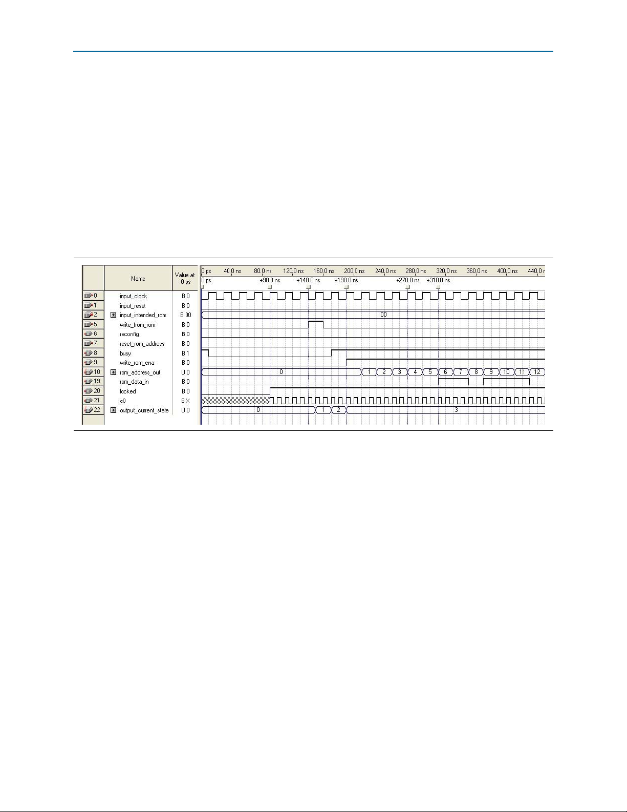
Figure 24 shows the simulation results when writing from ROM 1 to scan cache of the
ALTPLL_RECONFIG megafunction for the duration of 0 to 250 ns.
Figure 24. Initial Writing from ROM 1 to the Scan Cache of the ALTPLL_RECONFIG Megafunction (0 to 250 ns)
The simulation begins when the PLL gets locked (refer to Figure 24); the
is asserted at 90 ns. The PLL output
c0
produces a 100 MHz clock. The original
settings of the PLL have an input clock of 50 MHz and generates an output clock of
100 MHz.
1 The
output_current_state
signal is 0, which shows the current state of the state
machine that controls the PLL reconfiguration process from the external ROMs.
When the state machine is at
waiting for the assertion of the
value of the
input_intended_rom [1:0]
0
(indicated by the output_current_state signal), it is
input_want_to reconfig
signal together with the
signal, which is 00. The state machine
remains at this state until the above conditions are satisfied.
At 140 ns, the
input_intended_rom [1:0]
controls the
input_want_to_reconfig
signal is set to 00. The
write_from_rom
signal of the ALTPLL_RECONFIG instantiation. This
signal is asserted for 1 clock cycle and the
input_want_to_reconfig
begins the process of writing the contents of the intended ROM to the scan cache of
the ALTPLL_RECONFIG megafunction. The
used to control the selector (
sel [1:0]
signal) of the multiplexer instantiation, which
multiplexes the intended ROM contents (in this case, ROM 1) to the
input_intended_rom [1:0]
rom_data_in
signal of the ALTPLL_RECONFIG instantiation.
At 150 ns, the state machine is at
This signifies that the
the value of the
write_from_rom
also causes the selector (
input_want_to_reconfig
input_intended_rom [1:0]
signal of the ALTPLL_RECONFIG instantiation to be asserted. This
sel [1:0]
multiplex the intended ROM contents (in this case, ROM 1) to the
1
(indicated by the
output_current_state
signal has been asserted together with
signal, which is 00. This causes the
signal) of the multiplexer instantiation to
rom_data_in
of the ALTPLL_RECONFIG instantiation.
locked
signal
signal is
signal).
signal
signal
Phase-Locked Loop Reconfiguration (ALTPLL_RECONFIG) Megafunction February 2012 Altera Corporation
Page 31

Design Example Page 31
At 170 ns, the state machine is at 2 (indicated by the
this state, the state machine is waiting for the assertion of the
output_current_state
tapout_busy
signal). At
signal,
which signifies the busy signal of the ALTPLL_RECONFIG instantiation. The state
machine tracks the busy signal because whatever operation the ALTPLL_RECONFIG
is in (for example,
read_param, write_param, reconfig
, or
write_from_rom
) when
asserted for 1 clock cycle, the busy signal is asserted for a particular duration. This
indicates that the particular operation is being processed by the ALTPLL_RECONFIG
instantiation. In this state, the
the ALTPLL_RECONFIG instantiation has begun processing the
tapout_busy
signal has been asserted, signifying that
write_from_rom
operation.
At 190 ns, the state machine is at
This signifies that the
machine waits until the
tapout_busy
tapout_busy
3
(indicated by the
output_current_state
signal).
signal has been asserted. At this point the state
signal gets deasserted, to signify that the process
of writing from the ROM to the scan cache of the ALTPLL_RECONFIG instantiation
has been completed. Observe that the t
asserted. This is the probed-out signal of the
apout_rom_common_rden
write_rom_ena
signal, which is part of
signal has been
the ALTPLL_RECONFIG instantiation. This signal functions as the enable signal to
the ROMs used in this design. Observe that the
signal begins changing value. This is the probed-out signal of the
[7:0]
, which is part of the ALTPLL_RECONFIG instantiation. This signal controls
tapout_rom_common_address [7:0]
rom_address_out
which address of the ROM should be read out to the multiplexer instantiation. When
the
tapout_rom_common_rden
tapout_rom_common_address [7:0]
ROM 1 to the
q
port of the ROM, which is connected to the
signal is asserted together with the value of 0 for the
signal, it reads out the data from address 0 of the
data_0
signal of the
multiplexer. Then the data is multiplexed according to the selector of the multiplexer,
and sent out to the
port is probed out and is observed by the
rom_data_in
port of the ALTPLL_RECONFIG instantiation. This
tapout_rom_data_in
port. Therefore, the
data from the intended ROM can be observed in simulation.
1 The
tapout_rom_common_rden
tapout_busy
signal is asserted.
signal is asserted 1 clock cycle later, after the
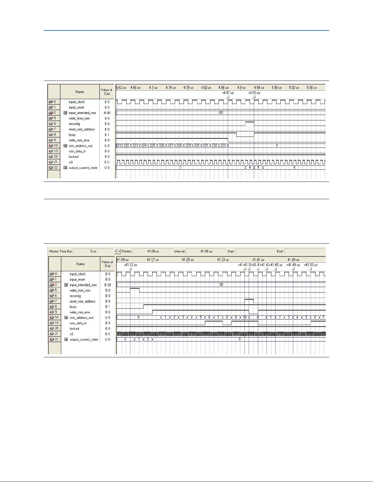
Figure 25 shows the simulation results when writing from ROM 1 to the scan cache of
the ALTPLL_RECONFIG megafunction for the duration of 60 to 580 ns.
Figure 25. Initial Writing from ROM 1 to the Scan Cache of the ALTPLL_RECONFIG Megafunction (60 to 580 ns)
Phase-Locked Loop Reconfiguration (ALTPLL_RECONFIG) MegafunctionFebruary 2012 Altera Corporation
Page 32

Page 32 Design Example
When data from the ROM is written to the scan cache of the ALTPLL_RECONFIG, it
is done serially, meaning a 1-by-1 bit per cycle, from address
observe this via the
tapout_rom_data_in
signal. The valid data read out from the
0
to address 233. You can
ROM is delayed by 2 clock cycles.
When the simulation is at 270 ns, the
the
tapout_rom_common_address [7:0]
tapout_rom_common_rden
signal is asserted with
signal with a value of 4. The data read out has
a value of 1 in the .mif file in Figure 25. However, this value only appears when the
tapout_rom_common_rden
[7:0]
signal with a value of 6 at 310 ns, implying a 2-clock-cycle delay.
This writing process continues until it has reached address
signal is asserted via the
tapout_rom_common_address
233
. Figure 26 shows the
simulation results of the final process in writing the contents of ROM 1 to the scan
cache of the ALTPLL_RECONFIG megafunction.
Figure 26. Ending Process of Writing the Contents of ROM 1 to the Scan Cache of the ALTPLL_RECONFIG Megafunction
(4700 to 5040 ns)
(1)
Note to Figure 26:
(1) This figure also shows the initialization of the reconfiguration process.
At 4850 ns, the
tapout_rom_common_rden
tapout_rom_common_address [7:0]
read out from ROM 1.
1 The data is available only 2 clock cycles later on the
tapout_rom_common_rden
output_current_state
tapout_busy
At 4870 ns, the
signal is deasserted.
tapout_rom_common_rden
signal and the
signal still has a value of 3. It will remain in this state until the
tapout_rom_common_address [7:0]
from reading out data; therefore, the address becomes 0. The
signal still generates valid output data and the
output_current_state
At 4890 ns, the
tapout_rom_common_rden
signal still has a value of 3.
tapout_rom_common_address [7:0]
tapout_rom_data_in
address 233). The
signal still has a value of
signal generates the last valid output data from ROM 1 (from
tapout_busy
signal is deasserted and the
3
.
signal is asserted with the
signal with a value of 233. This is the last address
tapout_rom_data_in
tapout_busy
signal are still asserted. The
signal. The
signal is deasserted with the
signal with a value of 0. This stops the ROM 1
tapout_busy
tapout_rom_data_in
signal is asserted. The
signal remains deasserted with the
signal with a value of0. Observe that the
output_current_state
Phase-Locked Loop Reconfiguration (ALTPLL_RECONFIG) Megafunction February 2012 Altera Corporation
Page 33

Design Example Page 33
At 4910 ns, the
tapout_rom_common_address [7:0]
1 The
tapout_rom_data_in
tapout_busy
value from
tapout_rom_common_rden
signal remains deasserted with the
signal with a value of0.
signal no longer generates valid output data. The
signal remains deasserted. The
3
to 4. In this state, the state machine is initiating the reconfiguration
output_current_state
signal changes
process.
You can observe this state by the assertion of the
cycle. This signal controls the
reconfig
signal of the ALTPLL_RECONFIG
tapout_reconfig
signal for 1 clock
instantiation. When this signal is asserted for 1 clock cycle, the ALTPLL_RECONFIG
instantiation begins the PLL reconfiguration process by using the settings written
from ROM 1 to the scan cache of the ALTPLL_RECONFIG instantiation.
At 4930 ns, the
asserted. This indicates that the state machine tracks the
machine tracks the
is in (for example
asserted for 1 clock cycle, the
tapout_reconfig
busy
signal because whatever operation the ALTPLL_RECONFIG
signal is deasserted and the
busy
tapout_busy
signal. The state
read_param, write_param, reconfig, write_from_rom
busy
signal is asserted for a particular duration. This
indicates that the particular operation is being processed by the ALTPLL_RECONFIG
instantiation. The
in this state until the
At 4950 ns, the
signal changes value from
output_current_state
tapout_busy
tapout_busy
5to6
signal is asserted.
signal remains asserted. The
. It remains in this state until the
signal changes value from 4to5. It remains
output_current_state
tapout_busy
deasserted.
signal is
) when
signal is
Figure 27 shows the final part of the reconfiguration process.
Figure 27. PLL Reconfiguration (10,000 to 10,400 ns)
Note to Figure 27:
(1) From c0 = 100 MHz to c0 = 200 MHz.
At 10,130 ns, the
tapout_busy
signal remains at a value of
tapout_busy
signal to be deasserted. The c0 signal is still at 100 MHz and the
signal remains asserted, which means the PLL is still locked to a 100-MHz signal.
(1)
signal remains asserted. The
6
. Therefore, the state machine is still waiting for the
output_current_state
locked
Phase-Locked Loop Reconfiguration (ALTPLL_RECONFIG) MegafunctionFebruary 2012 Altera Corporation
Page 34

Page 34 Design Example
At 10,170 ns, the
signal remains at a value of
tapout_busy
the PLL has lock loss, and the
At 10,190 ns, the
tapout_busy
signal remains asserted. The
6
. Therefore, the state machine is still waiting for the
signal to be deasserted. The
c0
signal is at a 0 value and not producing a clock pulse.
tapout_busy
signal is deasserted. This means the PLL
reconfiguration process is complete. The
value of
6
. The
locked
signal remains deasserted. The c0 signal is an unknown value
and still not producing a clock pulse.
At 10,210 ns, the
signal changes to a value of
tapout_busy
0
signal remains deasserted. The
. This is the original state, in which the state machine
waits for the next reconfiguration from an external ROM. The
deasserted. The
c0
signal is an unknown value and still does not produce a clock
pulse.
At 10,290 ns, the
signal remains at a value of
tapout_busy
0
signal remains deasserted. The
. The
locked
produces a 200-MHz clock signal, which is the intended setting from ROM 1.
Figure 28 through Figure 30 show the PLL reconfiguration process from the
remaining ROMs (ROM 2, ROM 3, and ROM 4, respectively).
Figure 28. PLL Reconfiguration from ROM 2 (20,330 to 20,600 ns)
output_current_state
locked
output_current_state
signal is deasserted, which means
signal remains at a
output_current_state
locked
signal remains
output_current_state
signal is asserted. The c0 signal now
(1)
Note to Figure 28:
(1) From c0 = 200 MHz to c0 = 300 MHz.
Phase-Locked Loop Reconfiguration (ALTPLL_RECONFIG) Megafunction February 2012 Altera Corporation
Page 35

Design Example Page 35
Figure 29. PLL Reconfiguration from ROM 3 (30,480 to 30,750 ns)
Note to Figure 29:
(1) From c0 = 300 MHz to c0 = 400 MHz.
Figure 30. PLL Reconfiguration from ROM 4 (40,800 to 41,090 ns)
(1)
(1)
Note to Figure 30:
(1) From c0 = 400 MHz to c0 = 500 MHz.
Phase-Locked Loop Reconfiguration (ALTPLL_RECONFIG) MegafunctionFebruary 2012 Altera Corporation
Page 36

Page 36 Design Example
The next part of the simulation demonstrates the PLL reconfiguration from ROM 1
again, but highlights the ROM address resetting capabilities during writing from an
external ROM to the scan cache of the ALTPLL_RECONFIG instantiation. The
c0
signal is 500 MHz and is reconfigured to 100 MHz. Figure 31 shows the process of
initiating writing the contents of ROM 1 to the ALTPLL_RECONFIG instantiation.
Figure 31. Initial Writing from ROM 1 to the Scan Cache of the ALTPLL_RECONFIG Megafunction (41,070 to 41,330 ns)
Figure 32 shows how the
Figure 32. Resetting the Address when Writing from ROM 1 to the Scan Cache of the ALTPLL_RECONFIG Megafunction
(41,200 to 41,450 ns)
At 41,250 ns, the
tapout_rom_common_rden
tapout_rom_common_address [7:0]
tapout_busy
signal is asserted. The
reset_rom_address
signal is asserted with the
signal with a value of 4. Observe that the
output_current_state
capability is used.
signal is 3. The normal
writing process from ROM to scan cache of the ALTPLL_RECONFIG instantiation
continues.
At 41,290 ns, the
tapout_rom_common_address [7:0]
tapout_rom_common_rden
signal with a value of 6. The
signal is asserted with the
tapout_rom_data_in
signal contains the valid data from address 4 because of the 2-clock-cycle delay. The
tapout_busy
At 41,380 ns, the
signal controls the
signal is asserted. The
output_current_state
input_main_reset_rom_address
reset_rom_address
of the ALTPLL_RECONFIG instantiation. It
signal is 3.
is asserted for 1 clock cycle. This
resets the address counter in the ALTPLL_RECONFIG instantiation to 0.
Phase-Locked Loop Reconfiguration (ALTPLL_RECONFIG) Megafunction February 2012 Altera Corporation
Page 37

Specifications Page 37
At 41,390 ns, the
tapout_rom_common_address [7:0]
tapout_rom_data_in
tapout_rom_common_rden
signal is changed to a value of 0. The
signal still generates the previous 2-clock-cycle output data
(address 9), which is of value 1. The
output_current_state
At 41,410 ns, the
tapout_rom_common_address [7:0]
signal is 3.
tapout_rom_common_rden
signal is changed to a value of0. This restarts the
writing of the contents of ROM 1 to the ALTPLL_RECONFIG scan cache from address
0. The
tapout_busy
signal is still asserted. The
The PLL reconfiguration process continues as normal until the
as shown in Figure 33.
Figure 33. PLL Reconfiguration From ROM1 (40,800 to 41,090 ns)
signal is deasserted for 1 clock cycle. The
tapout_busy
signal is still asserted. The
signal is reasserted. The
output_current_state
(1)
signal is 3.
c0
signal is 200 MHz,
Note to Figure 33:
(1) From c0 = 500 MHz to c0 = 200 MHz.
You can modify the design to suit your requirements when attempting to reconfigure
the PLL from multiple .mif files via external ROMs.
Specifications
This section describes the prototypes, component declarations, ports, and parameters
of the ALTPLL_RECONFIG megafunction. These ports and parameters are available
to customize the ALTPLL_RECONFIG megafunction according to your application.
Verilog HDL Prototype
The following Verilog HDL prototype is located in the Verilog Design File (.v)
altera_mf.v in the <Quartus II installation directory>\eda\synthesis directory.
modulealtpll_reconfig
#( parameterintended_device_family = "unused",
parameterinit_from_rom = "NO",
parameterpll_type = "UNUSED",
parameterscan_chain = "UNUSED",
parameterscan_init_file = "UNUSED",
Phase-Locked Loop Reconfiguration (ALTPLL_RECONFIG) MegafunctionFebruary 2012 Altera Corporation
Page 38

Page 38 Specifications
parameteruse_scanclk_sync_register = "NO",
parameterlpm_type = "altpll_reconfig",
parameterlpm_hint = "unused")
( outputwirebusy,
inputwireclock,
inputwire[2:0]counter_param,
inputwire[3:0]counter_type,
inputwire[8:0]data_in,
outputwire[8:0]data_out,
outputwirepll_areset,
inputwirepll_areset_in,
outputwirepll_configupdate,
outputwirepll_scanaclr,
outputwirepll_scanclk,
outputwirepll_scanclkena,
outputwirepll_scandata,
inputwirepll_scandataout,
inputwirepll_scandone,
outputwirepll_scanread,
outputwirepll_scanwrite,
inputwireread_param,
inputwirereconfig,
inputwirereset,
inputwirereset_rom_address,
outputwire[7:0]rom_address_out,
inputwirerom_data_in,
inputwirewrite_from_rom,
inputwirewrite_param,
outputwirewrite_rom_ena)/* synthesis syn_black_box=1 */;
endmodule //altpll_reconfig
VHDL Component Declaration
The following VHDL component declaration is located in the VHDL Design File
(.vhd) altera_mf_components.vhd in the <Quartus II installation
directory>\libraries\vhdl\altera_mf directory.
component altpll_reconfig
generic (
intended_device_family:string := "unused";
init_from_rom:string := "NO";
pll_type:string := "UNUSED";
Phase-Locked Loop Reconfiguration (ALTPLL_RECONFIG) Megafunction February 2012 Altera Corporation
Page 39

Specifications Page 39
scan_chain:string := "UNUSED";
scan_init_file:string := "UNUSED";
use_scanclk_sync_register:string := "NO";
lpm_hint:string := "UNUSED";
lpm_type:string := "altpll_reconfig"
);
port(
busy: out std_logic;
clock: in std_logic;
counter_param:in std_logic_vector(2 downto 0) := (others =>
'0');
counter_type:in std_logic_vector(3 downto 0) := (others =>
'0');
data_in:in std_logic_vector(8 downto 0) := (others => '0');
data_out:out std_logic_vector(8 downto 0);
pll_areset:out std_logic;
pll_areset_in:in std_logic := '0';
pll_configupdate:out std_logic;
pll_scanaclr:out std_logic;
pll_scanclk:out std_logic;
pll_scanclkena:out std_logic;
pll_scandata:out std_logic;
pll_scandataout:in std_logic := '0';
pll_scandone:in std_logic := '0';
pll_scanread:out std_logic;
pll_scanwrite:out std_logic;
read_param:in std_logic := '0';
reconfig:in std_logic := '0';
reset: in std_logic;
reset_rom_address:in std_logic := '0';
rom_address_out:out std_logic_vector(7 downto 0);
rom_data_in:in std_logic := '0';
write_from_rom:in std_logic := '0';
write_param:in std_logic := '0';
write_rom_ena:out std_logic
);
end component;
Phase-Locked Loop Reconfiguration (ALTPLL_RECONFIG) MegafunctionFebruary 2012 Altera Corporation
Page 40

Page 40 Specifications
Ports and Parameters
This section describes the ports and parameters of the ALTPLL_RECONFIG
megafunction.
Tab le 8 lists the ALTPLL_RECONFIG megafunction input ports.
Table 8. ALTPLL_RECONFIG Megafunction Input Ports (Part 1 of 3)
Port Name Required? Description
Clock input for loading individual parameters. This signal also clocks the PLL during
reconfiguration.
clock
reset
data_in[]
counter_type[]
counter_param[]
Yes
Yes
No
No
No
The clock input port must be connected to a valid clock.
Refer to the DC and Switching Characteristics chapter of the respective device
handbooks for the clock f
MAX
.
Asynchronous reset input to the megafunction.
Altera recommends that you reset this megafunction before first use to guarantee that
it is in a valid state. However, it does power up in the reset state. This port must be
connected.
Data input that provides parameter value when writing parameters.
A 9-bit input port that provides the data to be written to the scan cache during a write
operation. The bit width of the counter parameter to be written determines the
number of bits of
count of the
data_in[]
C0
counter is 8-bit wide, so
location. The bypass mode for the C0 counter is 1-bit wide, so
for the value of this parameter. If omitted, the default value is
that are read into the cache. For example, the low bit
data_in[7..0]
is read to the correct cache
data_in[0]
0
.
is read
Specifies the counter type.
An input port in the form of a 4-bit bus that selects which counter type should be
selected for the corresponding operation (
table specifies the mapping between the
read, write
counter_type
, or
reconfig
). The following
value and the physical
counter to be set. For details, refer to the following tables:
■ Table 11 on page 45
counter_type[3..0]
settings for Stratix III, Stratix IV, and
Cyclone III devices.
■ Table 13 on page 47
counter_type[3..0]
settings for Stratix II, Stratix II GX,
Arria GX and HardCopy II devices.
■ Table 14 on page 49
counter_type[3..0]
settings for Stratix and Stratix GX
devices.
Specifies the parameter for the value specified in the
counter_type
port.
An input port in the form of a 3-bit bus that selects which parameter for the given
counter type should be updated. The mapping to each parameter type and the
corresponding parameter bit-width are defined in the following tables:
■ Table 12 on page 46
counter_param[2..0]
settings for Stratix III, Stratix IV, and
Cyclone III devices.
■ Table 13 on page 47
counter_param[2..0]
settings for Stratix II, Stratix II GX,
Arria GX and HardCopy II devices.
■ Table 14 on page 49
counter_param[2..0]
settings for Stratix and Stratix GX
devices.
Phase-Locked Loop Reconfiguration (ALTPLL_RECONFIG) Megafunction February 2012 Altera Corporation
Page 41

Specifications Page 41
Table 8. ALTPLL_RECONFIG Megafunction Input Ports (Part 2 of 3)
Port Name Required? Description
read_param
write_param
No
No
Reads the parameter specified with the
from cache and fed to the
When asserted, the
and fed to
read and sent to
values. The
data_out[]
data_out[]
read_param
data_out[]
read_param
. The bit location of the scan cache and the number of bits
depend on the
signal is sampled at the rising clock edge. If it is asserted,
counter_type
port.
signal indicates that the scan cache should be read
counter_type
the parameter value is read from the cache. Assert the
cycle only to prevent the parameter from being read twice.
The
busy
signal is asserted on the rising clock edge following the assertion of
read_param
After the
parameter can be loaded. While the
data_out[]
When the
. While the parameter is being read, the
busy
signal is deasserted, the value on
busy
signal is asserted, the value on
is not valid.
read_param
signal is asserted, the
busy
following rising edge of the clock and not on the same clock cycle as
Writes the parameter specified with the
the cache with the value specified on the
When asserted, the
write_param
counter_type
data_in[]
signal indicates that the value on
should be written to the parameter specified by
counter_param[]
the parameter. The
. The number of bits read from the
write_param
signal is sampled at the rising clock edge. If it is
asserted, the parameter value is written to the cache. Assert the
for 1 clock cycle only to prevent the parameter from being written twice.
The
busy
signal is asserted on the rising clock edge following the assertion of
write_param
asserted and input to
. While the parameter is being written, the busy signal remains
data_in[]
is ignored. After the
and
counter_param
and
counter_param
read_param
busy
signal remains asserted.
data_out[]
signal for 1 clock
is valid and the next
signal is only asserted on the
read_param
and
counter_param
port.
data_in[]
counter_type[]
data_in[]
and
port depends on
write_param
busy
signal is deasserted, the
ports
.
ports to
signal
next parameter can be written.
When the
following rising edge of the clock and not on the same clock cycle as
write_param
signal is asserted, the
busy
signal is only asserted on the
write_param
.
Specifies that the phase-locked loop (PLL) should be reconfigured with the PLL
settings specified in the current cache.
When asserted, the
reconfig
with the values in the cache. The
If it is asserted, the cached settings are loaded in the PLL. Assert the
signal for 1 clock cycle only to prevent reloading the PLL configuration. The
signal is asserted on the rising clock edge following the assertion of
the PLL is being loaded, the
signal indicates that the PLL should be reconfigured
reconfig
signal is sampled at the rising clock edge.
reconfig
busy
reconfig
busy
signal remains asserted. After the
busy
signal is
. While
deasserted, the parameter values can be modified again.
reconfig
Yes
During and after reconfiguration, the scan chain data cache remains unchanged. This
allows you to easily create a new set of reconfiguration settings that differs from the
previous one in only one parameter.
If
write_param
Stratix II devices, the
has not been asserted since the previous assertion of
pll_scanwrite
signal is pulsed during reconfiguration. This
reconfig
, in
feature supports burst-phase stepping. However, in Stratix III, Stratix IV, Cyclone III,
Cyclone IV, and Arria II GX devices, the entire scan chain is shifted in to the PLL
again.
When the
following rising edge of the clock and not on the same clock cycle as
reconfig
signal is asserted, the
busy
signal is only asserted on the
reconfig
.
Phase-Locked Loop Reconfiguration (ALTPLL_RECONFIG) MegafunctionFebruary 2012 Altera Corporation
Page 42

Page 42 Specifications
Table 8. ALTPLL_RECONFIG Megafunction Input Ports (Part 3 of 3)
Port Name Required? Description
Input signal indicating that the PLL should be reset.
pll_areset_in
No
When asserted, the
be reset. This port defaults to
pll_areset_in
0
if left unconnected. When the ALTPLL_RECONFIG
signal indicates the PLL megafunction should
megafunction is used in a design, you cannot reset the PLL in any other way; you
must use this megafunction port to manually reset the PLL.
Input port for the ALTPLL_RECONFIG megafunction that signals update done from
the PLL module. This port is driven by the PLL's
scandone
output signal and
determines when the PLL is reconfigured.
pll_scandone
No
For Stratix III and Stratix IV devices,
and deasserted as soon as it detects the assertion of
completion of all PLL reconfiguration updates,
This is different than the
scandone
devices. In Stratix devices, the
scandone
signal is asserted for 1 clock cycle to mark the completion of PLL
pll_scandone
is asserted on most operations,
configupdate
scandone
is reasserted.
. Upon the
signal in older device families, such as Stratix
scandone
signal is deasserted most of the time. The
reconfiguration.
Input port driven by the
scandataout
signal from the ALTPLL megafunction. It can
be used to read the current configuration of the ALTPLL megafunction.
pll_scandataout
Yes
This input port holds the ALTPLL megafunction scan data output from the
dynamically reconfigurable bits. The
the
scandataout
when the
reconfig
port of the PLL. The activity on this port can only be observed
signal is asserted.
pll_scandataout
port must be connected to
Serial data input to the PLL from the ROM.
This 1-bit port allows the external ROM to be serially written into the scan cache of
the ALTPLL_RECONFIG megafunction. The value on this port is valid 2 clock cycles
rom_data_in
No
after the
after the
write_rom_ena
write_rom_ena
signal is asserted and remains valid until 2 clock cycles
signal is deasserted. This port is available for Stratix III,
Stratix IV, Cyclone III, Cyclone IV, HardCopy III, HardCopy IV, and Arria II GX devices
only.
Specifies that the scan chain must be written from the external ROM.
When asserted, this signal tells the ALTPLL megafunction to write the scan cache
from the external ROM. At the next rising clock edge, the ALTPLL_RECONFIG
write_from_rom
No
megafunction asserts the
addresses on the
rom_address_out
write_rom_ena
port. Assert the
signal and begins placing valid ROM
write_from_rom
signal for
1 clock cycle only. This port is available for Stratix III, Stratix IV, Cyclone III,
Cyclone IV, HardCopy III, HardCopy IV, and Arria II GX devices only.
Resets the ROM address.
When asserted, this signal tells the ALTPLL megafunction to restart the read from
reset_rom_address
No
ROM at address 0. Assert the
reset_rom_address
signal for 1 clock cycle only. This
port is available for Stratix III, Stratix IV, Cyclone III, Cyclone IV, HardCopy III,
HardCopy IV, and Arria II GX devices only.
Phase-Locked Loop Reconfiguration (ALTPLL_RECONFIG) Megafunction February 2012 Altera Corporation
Page 43

Specifications Page 43
Tab le 9 lists the ALTPLL_RECONFIG megafunction output ports.
Table 9. ALTPLL_RECONFIG Megafunction Output Ports (Part 1 of 2)
Port Name Required? Description
data_out[]
No
Data read from the cache when
9-bit output bus that provides the parameter data to the user. When the
signal is asserted, the values on
the parameter value that is loaded from cache and driven on the
When the megafunction deasserts the
(for example,
[0]
or
[3..0]
read_param
is asserted.
counter_type[]
busy
signal, the appropriate bits of the bus
) hold a valid value.
and
counter_param[]
read_param
determine
data_out[]
bus.
Indicates when the PLL is reading or writing a parameter to the cache, or is
configuring the PLL.
busy
No
While the
reconfiguration can be initiated. Changes to the megafunction can be made only
when the
write_param
specified operation is complete. In the case of a reconfiguration operation, the
signal remains high until the
Drives the
The
busy
signal is asserted, no parameters can be read or written, and no
busy
signal is not asserted. The signal goes high when the
, or
areset
pll_areset
reconfig
input port is asserted, and remains high until the
pll_areset
signal is asserted and then deasserted.
port on the PLL to be reconfigured.
port must be connected to the
areset
read_param
port of the ALTPLL
,
busy
megafunction for the reconfiguration to function correctly. This signal is active high.
pll_areset
Yes
pll_areset
at the next rising clock edge after the
is asserted when
pll_areset_in
scandone
is asserted, or, after reconfiguration,
signal goes high. If you use the
ALTPLL_RECONFIG megafunction, drive the PLL areset port using the
pll_areset
output port.
pll_configupdate
No
Drives the
configupdate
When asserted, the
configuration latches. The signal is asserted after the final data bit is sent out. This
port on the PLL to be reconfigured.
pll_configupdate
port loads selected data to PLL
port is available for Stratix III, Stratix IV, Cyclone III, Cyclone IV, HardCopy III,
HardCopy IV, and Arria II GX devices only.
pll_scanclk
Yes
Drives the
scanclk
For information about the maximum
port on the PLL to be reconfigured.
scanclk
frequency for the various devices,
refer to the respective device handbook.
pll_scanclkena
No
This acts as a clock enable for the
scanclk
Reconfiguration begins on the first rising edge of
pll_scanclkena
pll_scanclkena
is asserted. On the first falling edge of
signal is deasserted, the megafunction stops scanning data to the
port on the PLL to be reconfigured.
pll_scanclk
after
pll_scanclk
, after the
PLL.
pll_scanaclr
Yes
Drives the
scanaclr
Not available for Stratix II, Stratix III, Stratix IV, Cyclone III, Cyclone IV, HardCopy II,
port on the PLL to be reconfigured.
HardCopy III, HardCopy IV, Arria GX, and Arria II GX devices.
pll_scanread
No
Drives the
scanread
Not available for Stratix III, Stratix IV, Cyclone III, Cyclone IV, HardCopy III,
port on the PLL to be reconfigured.
HardCopy IV, and Arria II GX devices.
pll_scanwrite
No
Drives the
scanwrite
Not available for Stratix III, Stratix IV, Cyclone III, Cyclone IV, HardCopy III,
port on the PLL to be reconfigured.
HardCopy IV, and Arria II GX devices.
Phase-Locked Loop Reconfiguration (ALTPLL_RECONFIG) MegafunctionFebruary 2012 Altera Corporation
Page 44

Page 44 Specifications
Table 9. ALTPLL_RECONFIG Megafunction Output Ports (Part 2 of 2)
Port Name Required? Description
pll_scandata
Yes
Drives the
This output port from the megafunction holds the scan data input to the PLL for the
dynamically reconfigurable bits. The
Any activity on this port can only be observed when the
scandata
port on the PLL to be reconfigured.
pll_scandata
port sends scandata to the PLL.
reconfig
signal is asserted.
Specifies the address in ROM from which data is written to the scan chain.
During the write operation, the address increments from address 0 to the size of the
rom_address_out
No
scan cache. The
is asserted. Each address is asserted for 1 clock cycle. This port is available for
rom_address_out
port is valid only while the
write_rom_ena
port
Stratix III, Stratix IV, Cyclone III, Cyclone IV, HardCopy III, HardCopy IV, and Arria II
GX devices only.
Enables the ROM.
write_rom_ena
No
When the
write_rom_ena
megafunctions generates valid addresses on the
signal is asserted, the ALTPLL_RECONFIG
rom_address_out
port. This port
is available for Stratix III, Stratix IV, Cyclone III, Cyclone IV, HardCopy III,
HardCopy IV, and Arria II GX devices only.
Tab le 10 lists the ALTPLL_RECONFIG megafunction parameters.
Table 10. ALTPLL_RECONFIG Megafunction Parameters (Part 1 of 2)
Parameter Type Required? Description
Specifies initialization from ROM. Initializes on power-up and not after every
init_from_rom[]
String No
reset (to match RAM .mif file behavior). The available values are
NO
. If omitted, the default value is NO.
Specifies the type of PLL to instantiate. For Stratix III, Stratix IV, Cyclone III,
pll_type
String No
Cyclone IV, Arria II GX, HardCopy III, and HardCopy IV devices, values are
TOP_BOTTOM
and
LEFT_RIGHT
HardCopy II devices, values are
Specifies the valid PLL types. Available for Stratix and Stratix GX devices
scan_chain
String No
only. Values are
UNUSED
.
LONG, SHORT
Value Configuration Setting
LONG
SHORT
YES
. For Stratix II, Stratix II GX, Arria GX, and
ENHANCED
, and
and
FAST.
UNUSED
. If omitted, the default value is
288-bit scan chain used to control
PLLs with 12 counters
192-bit scan chain used to control
PLLs with 8 counters
and
Phase-Locked Loop Reconfiguration (ALTPLL_RECONFIG) Megafunction February 2012 Altera Corporation
Page 45

Specifications Page 45
Table 10. ALTPLL_RECONFIG Megafunction Parameters (Part 2 of 2)
Parameter Type Required? Description
Specifies the name of the .mif or .hex used as the initial value of the scan
UNUSED
chain cache. Values are <filename> and
every entry in the cache is
0
. You must set the input file as shown in the
. If omitted, the value for
following table:
Device Input File Size
scan_init_file
String No
Stratix series devices
(except Stratix III and Stratix IV
devices)
Stratix III and Stratix IV Top/Bottom
PLL devices
Stratix III and Stratix IV Right/Left
PLL devices
192 bits or 288 bits depending on
the
scan_chain
length
234 bits
180 bits
Cyclone III and Cyclone IV devices 144 bits
Arria II GX devices 180 bits
use_scanclk_sync_
register
String No
Specifies whether to use the
scanclk
the register. Available for all supported devices except Stratix III, Stratix IV,
Cyclone III, Cyclone IV, HardCopy III, HardCopy IV, and Arria II GX devices.
Values are
YES
and NO. If omitted, the default value is NO.
port for the synchronization mode for
Tab le 11 lists the
counter_type
settings for Stratix III, Stratix IV, Cyclone III,
Cyclone IV, and Arria II GX devices.
Table 11. counter_type[3..0] Settings for Stratix III, Stratix IV, Cyclone III, Cyclone IV, and
Arria II GX Devices (Part 1 of 2)
Counter Selection Binary Decimal
N
M
CP/LF
VCO
(1)
C0
(1)
C1
(1)
C2
(1)
C3
(1)
C4
(2)
C5
(2)
C6
(3)
C7
(3)
C8
(3)
C9
0000 0
0001 1
0010 2
0011 3
0100 4
0101 5
0110 6
0111 7
1000 8
1001 9
1010 10
1011 11
1100 12
1101 13
Illegal value 1110 14
Phase-Locked Loop Reconfiguration (ALTPLL_RECONFIG) MegafunctionFebruary 2012 Altera Corporation
Page 46

Page 46 Specifications
Table 11. counter_type[3..0] Settings for Stratix III, Stratix IV, Cyclone III, Cyclone IV, and
Arria II GX Devices (Part 2 of 2)
Counter Selection Binary Decimal
Illegal value 1111 15
Notes to Table 11:
(1) For Stratix III and Stratix IV Top/Bottom PLL, Stratix III and Stratix IV Left/Right PLL, and Cyclone III and
Cyclone IV PLL.
(2) For Stratix III and Stratix IV Top/Bottom PLL, Stratix III and Stratix IV Left/Right PLL, and Arria II GX PLL.
(3) For Stratix III and Stratix IV Top/Bottom PLL only.
Tab le 12 lists the
counter_param
settings for Stratix III, Stratix IV, Cyclone III,
Cyclone IV, and Arria II GX devices.
Table 12. counter_param[2..0] Settings for Stratix III, Stratix IV, Cyclone III, Cyclone IV, and
Arria II GX Devices
Counter Type Counter Param Binary Decimal Width (bits)
Regular counters
C0-C9: Top-Bottom
Stratix III and Stratix IV
High count 000 0 8
Low count 001 1 8
Bypass 100 4 1
C0-C6: Left-Right
Stratix III and Stratix IV
C0-C4: Cyclone III and
Mode (odd/even division) 101 5 1
Cyclone IV
C0-C6: Arria II GX
Charge pump unused 101 5 5
Charge pump current 000 0 3
CP/LF
Loop filter unused 100 4 1
Loop filter resistor 001 1 5
Loop filter capacitance 010 2 2
VCO VCO Post Scale 000 0 1
High count 000 0 8
Low count 001 1 8
M/N Counters
Bypass 100 4 1
Mode (odd/even division) 101 5 1
Nominal count 111 7 9
Note to Tab le 11 :
(1) For even nominal count, the counter bits are automatically set as follows:
■
high_count
■
low_count= Nominalcount
For odd nominal count, the counter bits are automatically set as follows:
■
high_count
■
low_count
■ odd/even division bit = 1
For nominal count = 1, Bypass bit = 1.
=
Nominalcount
= (
Nominalcount
=
Nominalcount
/2
/2
+ 1)/2
-
high_count
Phase-Locked Loop Reconfiguration (ALTPLL_RECONFIG) Megafunction February 2012 Altera Corporation
Page 47

Specifications Page 47
Tab le 13 lists the
counter_type
and
counter_param
settings for Stratix II,
Stratix II GX, Arria GX, and HardCopy II devices.
Table 13. counter_type and counter_param Settings for Stratix II, Stratix II GX, Arria GX, and
HardCopy II Devices (Part 1 of 2)
Counter Settings
4-bit bus that selects which counter type must be updated. The
following mapping determines which counter is specified for each
counter_type[]
counter_type
counter_type[3..0]
0000 (0x0)
0001 (0x1)
0010 (0x2)
0011 (0x3)
0100 (0x4)
0101 (0x5)
0110 (0x6)
0111 (0x7)
1000 (0x8)
1001 (0x9)
1010 (0xA)
1011 (0xB)
1100 (0xC)
1101 (0xD)
1110 (0xE)
1111 (0xF)
value.
Selected Counter
N [Enhanced PLL/ Fast PLL]
M [Enhanced PLL/ Fast PLL]
P/LF [Enhanced PLL/ Fast PLL]
(Illegal value)
C0 [Enhanced PLL/ Fast PLL]
C1 [Enhanced PLL/ Fast PLL]
C2 [Enhanced PLL/ Fast PLL]
C3 [Enhanced PLL/ Fast PLL]
C4 [Enhanced PLL]
C5 [Enhanced PLL]
(Illegal value)
(Illegal value)
(Illegal value)
(Illegal value)
(Illegal value)
(Illegal value)
Phase-Locked Loop Reconfiguration (ALTPLL_RECONFIG) MegafunctionFebruary 2012 Altera Corporation
Page 48

Page 48 Specifications
Table 13. counter_type and counter_param Settings for Stratix II, Stratix II GX, Arria GX, and
HardCopy II Devices (Part 2 of 2)
Counter Settings
3-bit bus that selects which parameter for the given counter type
should be updated. The mapping to each parameter type and the
corresponding parameter bit-width is defined as follows:
counter_param[]
Notes to Table 13:
(1) For Enhanced PLL M and N.
(2) For Enhanced PLL
(3) For Fast PLL
(4) For Fast PLL
C0-C5
(5) For
(6) For CP/LF.
C0-C5
C0-C3
and M.
N
.
, Fast PLL M.
counter_param[2..0]
000 (0x0)
001 (0x1)
000 (0x0)
001 (0x1)
000 (0x0)
001 (0x1)
000 (0x0)
010 (0x2)
100 (0x4)
101 (0x5)
101 (0x5)
000 (0x0)
001 (0x1)
010 (0x2)
011 (0x3)
110 (0x6)
111 (0x7)
.
Selected Parameter Width
nominal count
spread count
high cycles count
low cycles count
high cycles count
low cycles count
nominal count
(1)
(1)
(2)
(2)
(3)
(3)
(4)
phase step setting
counter bypass bit
counter odd division bit
spread counter bypass
charge pump current
loop filter resistor
loop filter capacitor
(5)
(1)
(6)
(6)
(6)
(illegal value)
(illegal value)
(illegal value)
9
9
8
8
4
4
2
2
1
1
1
4
6
2
—
—
—
Phase-Locked Loop Reconfiguration (ALTPLL_RECONFIG) Megafunction February 2012 Altera Corporation
Page 49

Specifications Page 49
Tab le 14 lists the
counter_type
and
counter_param
settings for Stratix and Stratix GX
devices.
Table 14. counter_type and counter_param Settings for Stratix and Stratix GX Devices (Part 1
of 2)
Counter Settings
4-bit bus that selects which counter type must be updated. The following
mapping determines which counter is specified for each
counter_type
value.
(1)
counter_type[]
counter_type[3..0]
0000 (0x0)
0001 (0x1)
0010 (0x2)
0011 (0x3)
0100 (0x4)
0101 (0x5)
0110 (0x6)
0111 (0x7)
1000 (0x8)
1001 (0x9)
1010 (0xA)
1011 (0xB)
1100 (0xC)
1101 (0xD)
1110 (0xE)
1111 (0xF)
Selected Counter
M
N
(Illegal value)
(Illegal value)
G0
G1
G2
G3
L0
L1
(Illegal value)
(Illegal value)
E1
E2
E3
E4
Phase-Locked Loop Reconfiguration (ALTPLL_RECONFIG) MegafunctionFebruary 2012 Altera Corporation
Page 50

Page 50 Document Revision History
Table 14. counter_type and counter_param Settings for Stratix and Stratix GX Devices (Part 2
of 2)
Counter Settings
3-bit bus that selects which parameter for the given counter type should
be updated. The mapping to each parameter type and the corresponding
parameter bit-width is defined as follows:
counter_param[2..0]
000 (0x0)
001 (0x1)
000 (0x0)
counter_param[]
001 (0x1)
010 (0x2)
011 (0x3)
100 (0x4)
101 (0x5)
110 (0x6)
111 (0x7)
Notes to Table 14:
(1) The lower 2 bits indicate the counter number for the G, L, and E counters. Additionally, the Ex counters are only
valid for the
(2) For
(3) For
(4) Must be 0 for
(5) The upper 2 bits determine the width (for example, 00× = 9, 01× = 4, 10× = 1)
M
and N.
G, L
, and E.
LONG
scan chain PLLs.
M
or N.
(5)
Selected Parameter Width
nominal count
spread count
high cycles count
low cycles count
delay element setting
(illegal value)
counter bypass bit
counter odd division bit
(illegal value)
(illegal value)
(2)
(2)
(3)
(3)
9
9
9
9
4
—
1
(4)
1
—
—
Document Revision History
Tab le 15 lists the revision history for this document.
Table 15. Document Revision History (Part 1 of 2)
Date Version Changes
February 2012 6.0
August 2010 5.0 Updated for the Quartus II software version 10.0.
July 2008 4.0
■ Added information about nominal count usage in Table 12.
■ Updated the decimal value in Table 12.
■ Added support for Stratix IV devices.
■ Updated screenshots for “MegaWizard Plug-In Manager Page Descriptions” section.
■ Updated “Features” section.
■ Updated “General Description” section.
■ Added “Simulation” section.
■ Added “Checking Design Violations With the Design Assistant” section
■ Added comment for pll_scanclk port.
■ Added support for new port, pllena.
Phase-Locked Loop Reconfiguration (ALTPLL_RECONFIG) Megafunction February 2012 Altera Corporation
Page 51

Document Revision History Page 51
Table 15. Document Revision History (Part 2 of 2)
Date Version Changes
■ Updated for the Quartus II software version 7.2, including: Added new user-mode
reconfiguration from external ROM.
■ Added three new input ports: rom_data_in, write_from_rom, and reset_rom_address
November 2007 3.2
■ Added two new output ports: rom_address_out and write_rom_ena
■ Updated design example format
■ Updated: Figure 5, Figure 6, Figure 7, Figure 17, Figure 18, Figure 19, Figure 20,
Figure 21, Figure 22
■ Changed altpll_reconfig to ALTPLL_RECONFIG throughout the document.
March 2007 3.1 Added Cyclone III to list of supported devices.
December 2006 3.0 Updated for Quartus II software version 6.1.
October 2006 2.0 Updated for Quartus II software version 6.0.
April 2005 1.0 Initial release.
Phase-Locked Loop Reconfiguration (ALTPLL_RECONFIG) MegafunctionFebruary 2012 Altera Corporation
 Loading...