

Page 1

PCI Compiler
User Guide
c The PCI Compiler is scheduled for product obsolescence and discontinued support
as described in PDN1410. Therefore, Altera does not recommend use of this IP in
new designs. For more information about Altera’s current IP offering, refer to
Altera’s Intellectual Property website.
101 Innovation Drive
San Jose, CA 95134
www.altera.com
Compiler Version: 11.1
Document Date: October 2011
Page 2

i–ii User Guide Version 11.1 Altera Corporation
PCI Compiler
Page 3

Copyright © 2011 Altera Corporation. All rights reserved. Altera, The Programmable Solutions Company, the stylized Altera logo,
ISO
9001:2008
Registered
Printed on recycled paper
specific device designations, and all other words and logos that are identified as trademarks and/or service marks are, unless noted
otherwise, the trademarks and service marks of Altera Corporation in the U.S. and other countries. All other product or service names
are the property of their respective holders. Altera products are protected under numerous U.S. and foreign patents and pending applications, maskwork rights, and copyrights. Altera warrants performance of its semiconductor products to current specifications in
accordance with Altera's standard warranty, but reserves the right to make changes to any products and services at any time without
notice. Altera assumes no responsibility or liability arising out of the application or use of any information, product, or service described herein except as expressly agreed to in writing by Altera Corporation. Altera customers are advised to obtain the latest
version of device specifications before relying on any published information and before placing orders for products or services.
UG-PCICOMPILER-4.12
iii Altera Corporation
i–iv User Guide Version 11.1 Altera Corporation
Page 4

PCI Compiler
Page 5

Contents
About PCI Compiler
Introduction ................................................................................................................................................ 1
Release Information ................................................................................................................................... 2
Device Family Support ............................................................................................................................. 2
Features ....................................................................................................................................................... 3
Common Features .................................................................................................................................. 3
PCI Compiler with MegaWizard Plug-in Manager Flow ................................................................4
PCI Compiler with SOPC Builder Flow ..............................................................................................4
General Description ................................................................................................................................... 5
PCI MegaCore Functions ......................................................................................................................5
PCI Testbench .........................................................................................................................................6
PCI Compiler with MegaWizard Plug-in Manager Flow ................................................................6
PCI Compiler With SOPC Builder Flow .............................................................................................7
Selecting the Appropriate Flow for Your Design ................................................................................. 9
PCI Compiler With SOPC Builder Flow .............................................................................................9
PCI Compiler With MegaWizard Plug-in Manager Flow .............................................................. 10
Compliance Summary ............................................................................................................................ 10
Performance and Resource Utilization ................................................................................................. 11
PCI Compiler with MegaWizard Plug-in Manager Flow ..............................................................11
PCI Compiler with SOPC Builder Flow ............................................................................................13
Installation and Licensing ...................................................................................................................... 17
OpenCore Plus Evaluation.................................................................................................................. 19
OpenCore Plus Time-Out Behavior...................................................................................................19
Section I. PCI Compiler With MegaWizard Plug-In Manager Flow
Chapter 1. Getting Started
Design Flow ............................................................................................................................................ 1–1
PCI MegaCore Function Design Walkthrough ................................................................................. 1–2
Create a New Quartus II Project .................................................................................................... 1–2
Launch IP Toolbench ....................................................................................................................... 1–4
Step 1: Parameterize ......................................................................................................................... 1–5
Step 2: Set Up Simulation ................................................................................................................ 1–7
Step 3: Generate ................................................................................................................................ 1–7
Simulate the Design ............................................................................................................................... 1–9
Simulation in the Quartus II Software ........................................................................................ 1–11
The Quartus II Simulation Files ......................................................................................................... 1–12
Master Simulation Files ................................................................................................................. 1–13
Target Simulation Files .................................................................................................................. 1–15
Altera Corporation v
Page 6

Contents
Compile the Design ............................................................................................................................. 1–16
Program a Device ................................................................................................................................ 1–18
PCI Timing Support ............................................................................................................................ 1–18
Using the Reference Designs .............................................................................................................. 1–19
pci_mt32 MegaCore Function Reference Design ....................................................................... 1–19
Synthesis & Compilation Instructions ................................................................................... 1–20
pci_mt64 MegaCore Function Reference Design ....................................................................... 1–21
synthesis & Compilation Instructions .................................................................................... 1–22
Chapter 2. Parameter Settings
Parameterize PCI Compiler ................................................................................................................. 2–1
PCI MegaCore Function Settings ........................................................................................................ 2–1
Read-Only PCI Configuration Registers ............................................................................................ 2–2
PCI Base Address Registers (BARs) .................................................................................................... 2–2
Advanced PCI MegaCore Function Features .................................................................................... 2–3
Optional Registers ....................................................................................................................... 2–3
Optional Interrupt Capabilities ................................................................................................. 2–4
Master Features ........................................................................................................................... 2–4
Variation File Parameters ..................................................................................................................... 2–7
Chapter 3. Functional Description
Functional Overview ............................................................................................................................. 3–1
Target Device Signals & Signal Assertion .................................................................................... 3–6
Master Device Signals & Signal Assertion .................................................................................... 3–9
PCI Bus Signals .................................................................................................................................... 3–11
Parameterized Configuration Register Signals .......................................................................... 3–15
Local Address, Data, Command, & Byte Enable Signals ......................................................... 3–16
Target Local-Side Signals .............................................................................................................. 3–20
Master Local-Side Signals ............................................................................................................. 3–24
PCI Bus Commands ............................................................................................................................ 3–27
Configuration Registers ...................................................................................................................... 3–28
Vendor ID Register ......................................................................................................................... 3–31
Device ID Register .......................................................................................................................... 3–31
Command Register ........................................................................................................................ 3–32
Status Register ................................................................................................................................ 3–33
Revision ID Register ...................................................................................................................... 3–34
Class Code Register ........................................................................................................................ 3–35
Cache Line Size Register ............................................................................................................... 3–35
Latency Timer Register .................................................................................................................. 3–36
Header Type Register .................................................................................................................... 3–36
Base Address Registers .................................................................................................................. 3–37
CardBus CIS Pointer Register ....................................................................................................... 3–40
Subsystem Vendor ID Register ....................................................................................................3–40
Subsystem ID Register ................................................................................................................... 3–41
Expansion ROM Base Address Register ..................................................................................... 3–41
Capabilities Pointer ........................................................................................................................ 3–42
Interrupt Line Register .................................................................................................................. 3–43
vi User Guide Version 11.1 Altera Corporation
PCI Compiler
Page 7

Contents
Interrupt Pin Register .................................................................................................................... 3–43
Minimum Grant Register .............................................................................................................. 3–43
Maximum Latency Register .......................................................................................................... 3–44
Target Mode Operation ...................................................................................................................... 3–44
Target Read Transactions .............................................................................................................. 3–48
Memory Read Transactions ..................................................................................................... 3–48
I/O Read Transactions ............................................................................................................. 3–61
Configuration Read Transactions ........................................................................................... 3–62
Target Write Transactions ............................................................................................................. 3–63
Memory Write Transactions .................................................................................................... 3–63
I/O Write Transactions ............................................................................................................ 3–75
Configuration Write Transactions .......................................................................................... 3–76
Target Transaction Terminations .................................................................................................3–77
Retry ............................................................................................................................................ 3–77
Disconnect .................................................................................................................................. 3–79
Target Abort ............................................................................................................................... 3–86
Additional Design Guidelines for Target Transactions ............................................................ 3–88
Master Mode Operation ..................................................................................................................... 3–88
PCI Bus Parking .............................................................................................................................. 3–92
Design Consideration ............................................................................................................... 3–92
Master Read Transactions ............................................................................................................. 3–93
Memory Read Transactions ..................................................................................................... 3–93
I/O & Configuration Read Transactions ............................................................................. 3–107
Master Write Transactions .......................................................................................................... 3–108
Memory Write Transactions .................................................................................................. 3–108
I/O & Configuration Write Master Transactions ............................................................... 3–124
Abnormal Master Transaction Termination ............................................................................. 3–125
Latency Timer Expires ............................................................................................................ 3–125
Retry .......................................................................................................................................... 3–125
Disconnect Without Data ....................................................................................................... 3–126
Disconnect with Data ............................................................................................................. 3–126
Target Abort ............................................................................................................................. 3–126
Master Abort ............................................................................................................................ 3–126
Host Bridge Operation ...................................................................................................................... 3–127
Using the PCI MegaCore Function as a Host Bridge .............................................................. 3–127
PCI Configuration Read Transaction from the pci_mt64 Local Master Device to the Internal
Configuration Space ............................................................................................................... 3–127
PCI Configuration Write Transaction from the pci_mt64 Local Master Device to the Internal
Configuration Space ............................................................................................................... 3–129
64-Bit Addressing, Dual Address Cycle (DAC) ............................................................................ 3–131
Target Mode Operation ............................................................................................................... 3–131
64-Bit Address, 64-Bit Data Single-Cycle Target Read Transaction ................................ 3–132
Master Mode Operation .............................................................................................................. 3–134
64-Bit Address, 64-Bit Data Master Burst Memory Read Transaction ............................ 3–134
Chapter 4. Testbench
General Description ............................................................................................................................... 4–1
Altera Corporation User Guide Version 11.1 vii
PCI Compiler
Page 8

Contents
Features ................................................................................................................................................... 4–2
PCI Testbench Files ............................................................................................................................... 4–2
Testbench Specifications ....................................................................................................................... 4–6
Master Transactor (mstr_tranx) ...................................................................................................... 4–7
PROCEDURES and TASKS Sections ........................................................................................ 4–7
INITIALIZATION Section ......................................................................................................... 4–8
USER COMMANDS Section ..................................................................................................... 4–8
Target Transactor (trgt_tranx) ................................................................................................. 4–12
FILE IO section .......................................................................................................................... 4–13
PROCEDURES and TASKS sections ...................................................................................... 4–13
Bus Monitor (monitor) ................................................................................................................... 4–14
Clock Generator (clk_gen) ............................................................................................................ 4–14
Arbiter (arbiter) .............................................................................................................................. 4–15
Pull Up (pull_up) ........................................................................................................................... 4–15
Local Reference Design ....................................................................................................................... 4–15
Local Target ..................................................................................................................................... 4–17
DMA Engine ................................................................................................................................... 4–17
Local Master .................................................................................................................................... 4–19
lm_lastn Generator ......................................................................................................................... 4–19
Prefetch ............................................................................................................................................ 4–19
LPM RAM ........................................................................................................................................ 4–19
Simulation Flow ................................................................................................................................... 4–20
Section II. PCI Compiler With SOPC Builder Flow
Chapter 5. Getting Started
Design Flow ............................................................................................................................................ 5–1
PCI Compiler with SOPC Builder Flow Design Walkthrough ....................................................... 5–2
Create a New Quartus II Project .................................................................................................... 5–3
Set Up the PCI-Avalon Bridge ........................................................................................................ 5–5
Add the Remaining Components to the SOPC Builder System ................................................ 5–7
Complete the Connections in SOPC Builder ................................................................................ 5–8
Generate the SOPC Builder System ............................................................................................... 5–9
Files Generated by SOPC Builder ................................................................................................ 5–10
Simulate the Design ............................................................................................................................. 5–11
Compile the Design ............................................................................................................................. 5–13
Program a Device ................................................................................................................................ 5–14
Upgrading Systems from a Previous Version ................................................................................. 5–15
Chapter 6. Parameter Settings
System Options-1 ................................................................................................................................... 6–1
PCI Device Mode ........................................................................................................................ 6–1
PCI Target Performance ............................................................................................................. 6–3
PCI Master Performance ............................................................................................................ 6–5
Value of Multiple Pending Reads ....................................................................................................... 6–6
viii User Guide Version 11.1 Altera Corporation
PCI Compiler
Page 9

Contents
System Options-2 ................................................................................................................................... 6–9
PCI Bus Speed .............................................................................................................................. 6–9
PCI Data Bus Width .................................................................................................................... 6–9
PCI Clock/Reset Settings ........................................................................................................... 6–9
PCI Bus Arbiter ......................................................................................................................... 6–10
PCI Configuration ............................................................................................................................... 6–11
PCI Base Address Registers ..................................................................................................... 6–11
PCI Read-Only Registers .........................................................................................................6–11
Setting the PCI Base Address Register Values ..................................................................... 6–11
Manual Setting of the BAR Size & Avalon Base Address ................................................... 6–14
Avalon Configuration ......................................................................................................................... 6–16
Chapter 7. Functional Description
Functional Overview ............................................................................................................................. 7–1
PCI-Avalon Bridge Blocks ............................................................................................................... 7–2
Avalon-MM Ports ....................................................................................................................... 7–3
Control/Status Register Module .............................................................................................. 7–5
PCI MegaCore Function ............................................................................................................. 7–5
PCI Bus Arbiter ........................................................................................................................... 7–6
Other PCI-Avalon Bridge Modules .......................................................................................... 7–6
PCI Operational Modes ................................................................................................................... 7–6
PCI Target-Only Peripheral Mode Operation ........................................................................ 7–6
PCI Master/Target Peripheral Mode Operation .................................................................... 7–8
PCI Host-Bridge Device Mode Operation ............................................................................. 7–10
Performance Profiles ...................................................................................................................... 7–11
Target Performance .................................................................................................................. 7–12
Master Performance .................................................................................................................. 7–12
Interface Signals ................................................................................................................................... 7–13
PCI Bus Arbiter Signals ................................................................................................................. 7–14
PCI Bus Commands ............................................................................................................................ 7–15
PCI Target Operation .......................................................................................................................... 7–15
Non-Prefetchable Operations ....................................................................................................... 7–17
Non-Prefetchable Write Operations ....................................................................................... 7–18
I/O Write Operations ............................................................................................................... 7–19
Non-Prefetchable Read Operations ........................................................................................ 7–19
Prefetchable Operations ................................................................................................................ 7–21
Prefetchable Write Operations ................................................................................................ 7–22
Prefetchable Read Operations ................................................................................................. 7–23
PCI-to-Avalon Address Translation ............................................................................................ 7–26
PCI Master Operation ......................................................................................................................... 7–27
Avalon-To-PCI Read & Write Operation .................................................................................... 7–28
Avalon-to-PCI Write Requests ................................................................................................ 7–31
Avalon-to-PCI Read Requests ................................................................................................. 7–32
Arbitration Among Pending PCI Master Requests .............................................................. 7–34
Avalon-to-PCI Address Translation ............................................................................................ 7–35
Ordering of Requests ..................................................................................................................... 7–38
Ordering of Avalon-to-PCI Operations ................................................................................. 7–39
Altera Corporation User Guide Version 11.1 ix
PCI Compiler
Page 10

Contents
Ordering PCI-to-Avalon Operations ...................................................................................... 7–42
PCI Host-Bridge Operation ................................................................................................................ 7–45
Altera-Provided PCI Bus Arbiter ...................................................................................................... 7–45
Interrupts .............................................................................................................................................. 7–46
Generation of PCI Interrupts ................................................................................................... 7–46
Reception of PCI Interrupts .....................................................................................................7–46
Generation of Avalon-MM Interrupts ................................................................................... 7–47
Control & Status Registers ................................................................................................................. 7–47
PCI Interrupt Status Register ........................................................................................................ 7–49
PCI Interrupt Enable Register ...................................................................................................... 7–51
PCI Mailbox Register Access ........................................................................................................ 7–52
Avalon-to-PCI Address Translation Table ................................................................................. 7–53
Read-Only Configuration Registers ............................................................................................ 7–54
Avalon-MM Interrupt Status Register ........................................................................................ 7–56
Avalon-MM Interrupt Enable Register ....................................................................................... 7–60
Avalon Mailbox Register Access ..................................................................................................7–60
Chapter 8. Testbench
General Description ............................................................................................................................... 8–1
Features ................................................................................................................................................... 8–2
PCI Testbench Files ............................................................................................................................... 8–3
Testbench Specifications ....................................................................................................................... 8–4
Master Transactor (mstr_tranx) ...................................................................................................... 8–5
PROCEDURES and TASKS Sections ........................................................................................ 8–5
INITIALIZATION Section ......................................................................................................... 8–6
USER COMMANDS Section ..................................................................................................... 8–7
cfg_rd ............................................................................................................................................ 8–7
cfg_wr ........................................................................................................................................... 8–8
mem_wr_32 .................................................................................................................................. 8–8
mem_rd_32 .................................................................................................................................. 8–9
mem_wr_64 ................................................................................................................................ 8–10
mem_rd_64 ................................................................................................................................ 8–11
io_wr ........................................................................................................................................... 8–11
io_rd ............................................................................................................................................ 8–11
Target Transactor (trgt_tranx) ...................................................................................................... 8–12
FILE IO section .......................................................................................................................... 8–13
PROCEDURES and TASKS sections ...................................................................................... 8–13
Bus Monitor (monitor) ................................................................................................................... 8–13
Arbiter (arbiter) .............................................................................................................................. 8–14
Pull Up (pull_up) ........................................................................................................................... 8–14
Simulation Flow ................................................................................................................................... 8–15
Appendix A. Using PCI Constraint File Tcl Scripts
Introduction ........................................................................................................................................... A–1
PCI Constraint Files .............................................................................................................................. A–1
Simultaneous Switching Noise (SSN) Considerations .................................................................... A–2
Additional Options ............................................................................................................................... A–3
x User Guide Version 11.1 Altera Corporation
PCI Compiler
Page 11

Contents
-speed ........................................................................................................................................... A–3
-no_compile ................................................................................................................................ A–7
-no_pinouts ................................................................................................................................. A–7
-pin_prefix ................................................................................................................................... A–7
-pin_suffix ................................................................................................................................... A–7
-help ............................................................................................................................................. A–8
Upgrading Assignments from a Previous Version of PCI Compiler ............................................ A–8
Upgrading PCI Assignments Containing Nondefault PCI Pin Names .................................. A–8
Additional Information
Revision History ............................................................................................................................... Info–i
How to Contact Altera .................................................................................................................... Info–ii
Typographic Conventions ............................................................................................................. Info–iii
Altera Corporation User Guide Version 11.1 xi
PCI Compiler
Page 12

Contents
xii User Guide Version 11.1 Altera Corporation
PCI Compiler
Page 13

About PCI Compiler
Introduction
The Altera® PCI Compiler provides many options for creating custom,
high-performance PCI bus interface designs. Whether your system’s top
priority is high bandwidth, high speed, or a combination of features, you
can use the PCI Compiler to meet your system requirements.
The PCI Compiler contains the pci_mt64, pci_mt32, pci_t64, and
®
pci_t32 MegaCore
functions, a Verilog HDL and VHDL testbench, and
reference designs. Altera also offers the following development kits as
PCI hardware prototyping platforms:
■ PCI High-Speed Development Kit, Stratix Professional Edition
■ PCI Development Kit, Cyclone II Edition
These kits include a PCI development board, a reference design, software
drivers, and a graphical user interface to help you evaluate the PCI
solution in a system.
You can create PCI systems using one of the following design flows in the
®
Quartus
■ MegaWizard
II software.
TM
Plug-in Manager flow
This option allows you to choose a specific PCI MegaCore function,
specify parameters, generate design files, and manually integrate the
parameterized PCI MegaCore function into your overall system.
■ SOPC Builder flow
This option allows you to build a complete PCI system—componentby-component—using an automatically-generated sytem
interconnect fabric. The SOPC Builder uses the PCI-Avalon®Memory-Mapped (Avalon-MM) bridge to connect the PCI bus to the
interconnect, allowing you to easily create any system that includes
one or more of the Avalon-MM peripherals.
Altera Corporation User Guide Version 11.1 1
October 2011
Page 14

Release Information
Release
Information
Device Family Support
Ta bl e 1 provides information about this release of the PCI Compiler.
Table 1. PCI Compiler User Guide Release Information
Item Description
Version 11.1
Release Date October 2011
Ordering Codes IP-PCI/MT64, IP-PCI/T64,
Product IDs
Vendor ID 6AF7
The MegaCore functions provide either final or preliminary support for
target Altera device families:
■ Final support means the core is verified with final timing models for
this device family. The core meets all functional and timing
requirements for the device family and can be used in production
designs.
■ Preliminary support means the core is verified with preliminary
timing models for this device family. The core meets all functional
requirements, but might still be undergoing timing analysis for the
device family. It can be used in production designs with caution.
■ HardCopy Compilation means the core is verified with final timing
models for the HardCopy
functional and timing requirements for the device family and can be
used in production designs.
■ HardCopy Companion means the core is verified with preliminary
timing models for the HardCopy companion device. The core meets
all functional requirements, but might still be undergoing timing
analysis for HardCopy device family. It can be used in production
designs with caution.
IP-PCI/MT32, IP-PCI/T32
pci_mt64 MegaCore function: 0011,
pci_t64 MegaCore function: 0025,
pci_mt32 MegaCore function: 0022,
pci_t32 MegaCore function: 0024
®
device family. The core meets all
2 User Guide Version 11.1 Altera Corporation
PCI Compiler October 2011
Page 15

About PCI Compiler
Ta bl e 2 shows the level of support offered by the User Guide MegaCore
functions for each Altera device family.
Table 2. Device Family Support
Device Family Support
Arria®GX
Arria II GX Final
®
Cyclone
Cyclone II Final
Cyclone III Final
Cyclone III LS Final
Cyclone IV (E, GX) Final
HardCopy II HardCopy Compilation
HardCopy III
HardCopy IV (E, GX)
®
II (1)
MAX
®
Stratix
Stratix GX Final
Stratix II Final
Stratix II GX Final
Stratix III Final
IV (E, GX)
Stratix
Other device families No support
Note to Ta b l e 2:
(1) MAX II devices are supported by the pci_mt32 and pci_t32 MegaCore
functions only.
Final
Final
Refer to the What’s New in Altera IP
page of the Altera website.
Final
Final
Final
Features
This section summarizes the features of the PCI Compiler.
Common Features
The following list outlines the common features of the PCI Compiler.
■ Fully compliant with the PCI Special Interest Group (PCI SIG)
PCI Local Bus Specification, Revision 3.0
■ Supports both 32-bit and 64-bit interfaces
■ Supports Master/Target and Target-Only modes
Altera Corporation User Guide Version 11.1 3
October 2011
Page 16

Features
■ IP functional simulation models enable simulation of a register
transfer level (RTL) model of a PCI MegaCore function in VHDL and
Verilog HDL simulators
■ OpenCore Plus hardware evaluation feature enables testing of a
PCI MegaCore function in hardware prior to purchasing a license
■ Configuration registers:
● Parameterized registers: device ID, vendor ID, class code,
revision ID, BAR0 through BAR5, subsystem ID, subsystemvendor ID, maximum latency, minimum grant, capabilities list
pointer, expansion ROM BAR
● Parameterized default or preset base address (available for all
six BARs) and expansion ROM base address
● Non-parameterized registers: command, status, header type 0,
latency timer, cache line size, interrupt pin, interrupt line
■ Host bridge application support
PCI Compiler with MegaWizard Plug-in Manager Flow
The following list outlines the features of the PCI Compiler with
MegaWizard Plug-in Manager flow.
■ IP Toolbench wizard-driven interface makes it easy to generate a
custom variation of a PCI MegaCore function
■ PCI target features:
● Capabilities list pointer support
● Expansion ROM BAR support
● Local-side requests for target abort, retry, or disconnect
● Local-side interrupt requests
■ PCI master features (pci_mt64 and pci_mt32 only):
● Allows on-chip arbitration logic
● Allows disabling latency timer
■ 64-bit PCI features (pci_mt64 and pci_t64 only):
● 64-bit addressing support as both master and target
● Initiates 64-bit addressing, using dual-address cycle (DAC)
● Initiates 64-bit memory transactions
● Dynamically negotiates 64-bit transactions and automatically
multiplexes data on the local 64-bit data bus
PCI Compiler with SOPC Builder Flow
The following list outlines the features of the PCI Compiler with SOPC
Builder flow.
■ SOPC Builder ready
■ PCI complexities, such as retry and disconnect are handled by the
PCI/Avalon Bridge logic and transparent to the user
4 User Guide Version 11.1 Altera Corporation
PCI Compiler October 2011
Page 17

About PCI Compiler
■ Hard-coded (fixed) or run-time configurable (dynamic) Avalon-to-
PCI address translation
■ Hard-coded or automatic PCI-to-Avalon address translation
■ Separate Avalon Memory-mapped (Avalon-MM) slave ports for PCI
bus access (PBA) and control register access (CRA)
■ Support for Avalon-MM burst mode
■ Option for independent or common PCI and Avalon clock domains
■ Option to increase PCI read performance by increasing the number
of pending reads and maximum read burst size.
■ Internal Arbiter in Host Bridge and Target/Master mode
General Description
This section provides a general description of the following:
■ PCI MegaCore Functions
■ PCI Testbench
■ PCI Compiler with MegaWizard Plug-in Manager Flow
■ PCI Compiler with SOPC Builder Flow
PCI MegaCore Functions
The PCI MegaCore functions are hardware-tested, high-performance,
flexible implementations of PCI interfaces. These functions handle the
PCI protocol and timing requirements internally. The back-end interface
is designed for easy integration, allowing you to focus your engineering
efforts on value-added custom development to significantly reduce timeto-market.
Optimized for Altera devices, the PCI MegaCore functions support
configuration, I/O, and memory transactions. The small size of the
functions, combined with the high density of Altera's devices, provides
ample resources for custom local logic to accompany the PCI interface.
The high performance of Altera's devices also enables these functions to
support unlimited cycles of zero wait state memory-burst transactions.
These functions can operate at either 33- or 66-MHz PCI bus clock speeds,
allowing them to achieve up to 132 Megabytes per second (MBytes/s)
throughput in a 32-bit 33-MHz PCI bus system and up to 528 MBytes/s
throughput in a 64-bit 66-MHz PCI bus system.
In the pci_mt64 and pci_mt32 functions, the master and target
interfaces can operate independently, allowing maximum throughput
and efficient usage of the PCI bus. For instance, while the target interface
is accepting zero wait state burst write data, the local logic may
simultaneously request PCI bus mastership, thus minimizing latency.
Altera Corporation User Guide Version 11.1 5
October 2011
Page 18

General Description
To ensure timing and protocol compliance, the PCI MegaCore functions
have been rigorously hardware tested. Refer to “Compliance Summary”
on page 10 for more information on the hardware tests performed.
PCI Testbench
The PCI testbench, provided in Verilog HDL and VHDL, facilitates the
design and verification of systems that implement any of the PCI
MegaCore functions. You can build a PCI behavioral simulation
environment by using components of the PCI testbench, the IP functional
simulation model of your PCI MegaCore function variation, and the rest
of your Verilog HDL or VHDL design.
PCI Compiler with MegaWizard Plug-in Manager Flow
With this flow, you design to a low-level interface that allows custom PCI
transaction design. Because you are designing the logic to interface to the
PCI MegaCore function, you have more control of individual module
functionality.
1 This flow is recommended for users who have previously
designed with the PCI Compiler or whose highest priority is to
minimize design latency.
For example, if you are designing a PCI-to-DDR2 SDRAM controller
interface you need to do the following:
■ Specify the PCI MegaCore function parameters.
■ Design the ‘back end’ user design, including master control logic,
target control logic, data path first-in first-out (FIFO) buffers, and
direct memory access (DMA) engine.
■ Design the DDR2 SDRAM controller interface.
■ Specify the DDR2 SDRAM MegaCore function parameters.
■ Design internal PCI and DDR2 SDRAM logic blocks.
■ Write RTL code that connects the PCI and DDR2 SDRAM blocks.
6 User Guide Version 11.1 Altera Corporation
PCI Compiler October 2011
Page 19
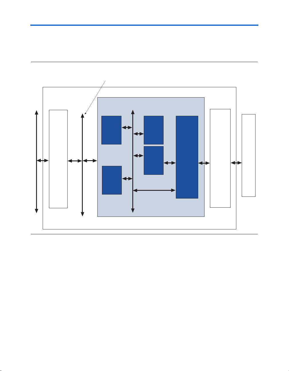
Figure 1 shows a PCI-to-DDR2 SDRAM controller interface design using
Master
Control
Logic
Backend User Design
Altera
PCI
MegaCore
Function
PCI
Bus
Altera PCI MegaCore Function Local-Side, Low Level Interface
DDR2 SDRAM Memory Module
DMA
Engine
Tar ge t
Control
Logic
Data
Path
FIFOs
DDR2
SDRAM
Controller
Interface
Altera FPGA
Altera
DDR2
SDRAM
Controller
MegaCore
Function
the PCI Compiler with MegaWizard Plug-in Manager flow; shaded areas
represent user-customized blocks.
Figure 1. PCI-to-DDR2 SDRAM Design Using the PCI Compiler With MegaWizard Flow
About PCI Compiler
f For more information about the PCI Compiler with MegaWizard flow,
refer to Chapter 1, Getting Started.
PCI Compiler With SOPC Builder Flow
With this flow, you specify system components and choose system
options from a rich set of features, and the SOPC Builder then
automatically generates the interconnect logic and simulation
environment. Thus, you define and generate a complete system in
dramatically less time than manually integrating separate IP blocks.
Altera Corporation User Guide Version 11.1 7
October 2011
1 This flow is recommended for users who are new to the PCI
Compiler or whose highest priority is to minimize design time.
Page 20
General Description
PCI
Bus
PCI Master/Target
Component
DMA
Engine
Altera FPGA
DDR2
SDRAM
Memory
Module
Altera
DDR2
SDRAM
MegaCore
Function
System
Interconnect
Fabric
PCI-Avalon
Bridge
Logic
Altera
PCI
MegaCore
Function
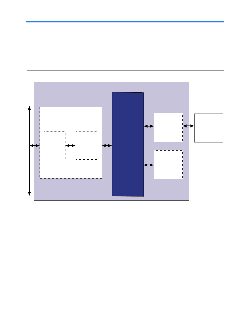
For example, Figure 2 shows the PCI-to-DDR2 SDRAM design using the
PCI Compiler with SOPC Builder flow; the dashed-lines indicate
pre-existing components that are added to the design via the SOPC
Builder graphical user interface (GUI). When comparing Figure 1 with
Figure 2, you can see that the PCI Compiler with SOPC Builder flow
option requires far less user customization.
Figure 2. PCI-to-DDR2 SDRAM Design Using the PCI Compiler With SOPC Builder Flow
f For more information about the PCI Compiler with SOPC Builder flow,
refer to Chapter 5, Getting Started.
8 User Guide Version 11.1 Altera Corporation
PCI Compiler October 2011
For more information about SOPC Builder, refer to volume 4 of the
Quartus II Handbook.
Page 21

About PCI Compiler
Selecting the Appropriate Flow for Your Design
Ta bl e 3 summarizes the guidelines for selecting a particular flow over
another. In most cases, the PCI Compiler with SOPC Builder flow is the
appropriate choice.
Table 3. PCI Compiler Parameterization Flow Selection Guidelines
SOPC Builder Flow MegaWizard Plug-in Manager Flow
● You would like to quickly integrate
multiple system blocks.
● You are creating a new PCI design.
● You have limited PCI bus protocol
experience.
● You are migrating a design that
uses a previous version of PCI
Compiler.
● You require features that are not
supported with the SOPC Builder
flow.
PCI Compiler With SOPC Builder Flow
This section lists the advantages and disadvantages of the PCI Compiler
with the SOPC Builder flow.
Advantages
■ Dramatically faster time-to-market
■ Requires minimal PCI bus protocol design expertise
■ Very short learning curve
■ Access to rich feature set
■ Uses simple and flexible GUI to create complete PCI system within
hours
■ Predesigned ‘back end’ and ‘local side’ interconnect
■ Uses an automatically-generated simulation environment
■ Create custom components and integrate them by using the
component wizard
■ All components are automatically interconnected
Disadvantages
■ Does not allow you to customize PCI transaction behavior
■ Some applications may have excessive overhead in size and
performance
Altera Corporation User Guide Version 11.1 9
October 2011
Page 22

Compliance Summary
PCI Compiler With MegaWizard Plug-in Manager Flow
This section lists the advantages and disadvantages of the PCI Compiler
with MegaWizard Plug-in Manager flow.
Advantages
■ More control of the system feature set
■ Can design directly from the PCI interface to peripheral devices
■ Can access local-side interface to reduce clock cycles and achieve
higher bandwidth
Disadvantages
■ Requires manual integration of system modules
■ Cannot easily use existing SOPC Builder peripherals
■ Requires a register transfer level (RTL) file for each instantiation
■ Requires significant knowledge of the PCI bus protocol
Compliance
Summary
The MegaCore functions are compliant with the requirements specified in
the PCI SIG PCI Local Bus Specification, Revision 3.0 and Compliance
Checklist, Revision 3.0.
To ensure PCI compliance, Altera has performed extensive validation of
the PCI MegaCore functions. Validation includes both simulation and
hardware testing. The following simulations are covered by the
validation suite for the PCI MegaCore functions:
■ PCI-SIG checklist simulations
■ Applicable operating rules in Appendix C of the PCI Local Bus
Specification, Revision 3.0, including:
● Basic protocol
● Signal stability
● Master and target signals
● Data phases
● Arbitration
● Latency
● Device selection
● Parity
■ Local-side interface functionality
■ Corner cases of the PCI and local-side interface, such as random wait
state insertion
In addition to simulation, Altera performed extensive hardware testing
on the functions to ensure robustness and PCI compliance. The test
platforms include the Agilent E2928A PCI Bus Exerciser and Analyzer, an
Altera PCI development board with a device configured with a PCI
MegaCore function and a reference design, and PCI bus agents such as a
10 User Guide Version 11.1 Altera Corporation
PCI Compiler October 2011
Page 23

About PCI Compiler
host bridge, Ethernet network adapter, and video card. The Altera PCI
MegaCore functions were tested on the Stratix EP1S25F1020C5 and
EP1S60F1020C6 devices. Hardware testing ensures that the PCI
MegaCore functions operate flawlessly under the most stringent
conditions.
During hardware testing with the Agilent E2928A PCI Bus Exerciser and
Analyzer, various tests were performed to guarantee robustness and
strict compliance. These tests included the following:
■ Memory read/write
■ I/O read/write
■ Configuration read/write
The tests generate random transaction types and parameters at the PCI
and local sides. The Agilent E2928A PCI Bus Exerciser and Analyzer
simulated random behavior on the PCI bus by randomizing transactions
with variable parameters such as the following:
■ Bus commands
■ Burst length
■ Data types
■ Wait states
■ Terminations
■ Error conditions
The local side also emulated a variety of test conditions in which the PCI
MegaCore functions experienced random wait states and terminations.
During the tests, the Agilent E2928A PCI Bus Exerciser and Analyzer also
acted as a PCI protocol and data integrity checker as well as a logic
analyzer to aid in debugging. This testing ensures that the functions
operate under the most stringent conditions in your system.
f For more information on the Agilent E2928A PCI Bus Exerciser and
Analyzer, refer to the Agilent website at www.agilent.com.
Performance
This section lists the speed and approximate resource utilization of the
PCI MegaCore functions in supported Altera device families.
and Resource
Utilization
Altera Corporation User Guide Version 11.1 11
October 2011
PCI Compiler with MegaWizard Plug-in Manager Flow
The speed and resource utilization estimates are based on a PCI
MegaCore function using one BAR that reserves 1 MByte of memory.
Implementing additional BARs generates additional logic in the PCI
Page 24

Performance and Resource Utilization
MegaCore function. Using different parameter options may result in
additional logic generated within the function. Results were generated
using the Quartus II software version 11.1.
Ta bl e 4 shows PCI MegaCore function resource utilization and
performance data for Stratix II devices.
Table 4. PCI MegaCore Function Performance in Stratix II Devices (1)
PCI Function
pci_mt64
pci_t64
pci_mt32
pci_t32
Notes to Ta b l e 4:
(1) This data was obtained by compiling each of the PCI MegaCore functions
(parameterized to use one BAR that reserves 1 MByte of memory) in the Stratix II
EP2S60F1020C5 device.
(2) The Utilization for Stratix II devices is based on the number of adaptive look-up
tables (ALUTs) used for the design as reported by the Quartus II software.
Utilization
(ALUTs) (2)
1,083 89 > 67
714 87 > 67
754 50 > 67
448 48 > 67
I/O Pins
f
MAX
(MHz)
Ta bl e 5 shows PCI MegaCore function resource utilization and
performance for Stratix, Stratix GX, and Cyclone devices.
Table 5. PCI MegaCore Function Performance in Stratix, Stratix GX &
Cyclone Devices (1)
PCI Function
pci_mt64
pci_t64
pci_mt32
pci_t32
Logic Elements
(LEs)
1,378 89 > 67
966 87 > 67
1007 50 > 67
661 48 > 67
I/O Pins
f
MAX
(MHz)
Note to Ta b l e 5:
(1) The PCI MegaCore functions use approximately the same number of LEs for the
Stratix, Stratix GX, and Cyclone device families. This data was obtained by
compiling each of the PCI MegaCore functions (parameterized to use one BAR
that reserves 1 MByte of memory) in the Stratix EP1S60F1020C6 device.
12 User Guide Version 11.1 Altera Corporation
PCI Compiler October 2011
Page 25

About PCI Compiler
Ta bl e 6 shows PCI MegaCore function resource utilization and
performance data for Cyclone II devices.
Table 6. PCI MegaCore Function Performance in Cyclone II Devices (1)
PCI Function
pci_mt64
pci_t64
pci_mt32
pci_t32
Note to Ta b l e 6:
(1) This data was obtained by compiling each of the PCI MegaCore functions
(parameterized to use one BAR that reserves 1 MByte of memory) in the
Cyclone II EP2C35F672C7 device.
Logic Elements
(LEs)
1,219 89 > 67
778 87 > 67
847 50 > 67
504 48 > 67
I/O Pins
f
MAX
(MHz)
Ta bl e 7 shows PCI MegaCore function resource utilization and
performance for MAX II devices.
Table 7. PCI MegaCore Function Performance in MAX II Devices (1), (2)
PCI Function
pci_mt32
pci_t32
Notes to Ta b l e 7:
(1) This data was obtained by compiling each of the PCI MegaCore functions
(parameterized to use one BAR that reserves 1 MByte of memory) in the MAX II
EPM2210F324C3 device.
(2) pci_mt64 and pci_t64 MegaCore functions are not supported in MAX II
devices.
Logic Elements
(LEs)
789 50 > 67
455 48 > 67
I/O Pins
f
MAX
(MHz)
PCI Compiler with SOPC Builder Flow
The speed and resource utilization estimates are for the supported
devices when operating in the PCI Target-Only, PCI Master/Target, and
PCI Host-Bridge device modes for each of the application-specific
performance settings.
1 Performance results will vary depending on the user-specified
parameters that are built into the system module.
Altera Corporation User Guide Version 11.1 13
October 2011
Page 26

Performance and Resource Utilization
Ta bl e 8 lists memory utilization and performance data for Stratix II
devices.
Table 8. Memory Utilization & Performance Data for Stratix II Devices (4)
Performance Setting
as: (1)
PCI
Device
Mode
PCI
TargetOnly
PCI
Master/
Target
Notes to Ta b l e 8:
(1) Min = Single-cycle transactions
Ty pi ca l = Burst transactions with a single pending read
Max = Burst transactions with multiple pending reads
(2) The LE count for Stratix II devices is based on the number of adaptive look-up tables (ALUTs) used for the design as
reported by the Quartus II software.
(3) In some compilations one M512 block was used, but it is not counted.
(4) The data was obtained by performing compilations on a Stratix II EP2S60F1020C5 device. Each of the device types
was parameterized to use one BAR that reserved 1 MByte of memory on the Avalon-MM side. For the PCI
Master/Target Peripheral mode, one MByte of memory was reserved on the PCI side.
PCI Target
Min N/A 543 0 48 767 0 87 >67
Typical N/A 886 4 48 1,165 6 87 >67
Max N/A 1,240 4 48 1,556 68 87 >67
Min Typical 1,726 6 50 2,393 9 89 >67
Typical Typical 1,953 8 50 2,729 123 89 >67
Max Typical 2,321 8 50 3,114 12 89 >67
Min Max 2,532 9 50 3,665 15 89 >67
Typical Max 2,753 11 50 3,989 18 89 >67
Max Max 3,149 11 50 4,350 18 89 >67
PCI
Master
32-Bit PCI Interface 64-Bit PCI Interface
M4K
Utilization
ALUTs(2)
Memory
Blocks
I/O
Pins
Utilization
ALUTs(2)
Memory
(3)
M4K
Blocks
(3)
I/O
Pins
PCI
f
MAX
(MHz)
14 User Guide Version 11.1 Altera Corporation
PCI Compiler October 2011
Page 27

Ta bl e 9 lists memory utilization and performance data for Cyclone II
devices.
Table 9. Memory Utilization & Performance Data for Cyclone II Devices (2)
About PCI Compiler
Performance Setting as: (1) 32-Bit PCI Interface 64-Bit PCI Interface
I/O
PCI
f
MAX
(MHz)
PCI
Device
Mode
PCI Target PCI Master
Logic
Elements
(LEs)
PCI
TargetOnly
PCI
Master/
Target
Notes to Ta b l e 9:
(1) Min = Single-cycle transactions
(2) The data was obtained by performing compilations on a Cyclone II EP2C35F672C7 device. Each of the device types
Min N/A 547 0 48 1,114 0 87 >67
Typical N/A 1,113 4 48 1,565 6 87 >67
Max N/A 1,605 4 48 2,051 6 87 >67
Min Typical 2,117 7 50 3,075 9 89 >67
Typical Typical 2,319 9 50 3,391 13 89 >67
Max Typical 2,806 9 50 3,915 13 89 >67
Min Max 3,096 7 50 4,655 9 89 >67
Typical Max 3,328 9 50 4,939 13 89 >67
Max Max 3,806 9 50 5,454 13 89 >67
Ty pi ca l = Burst transactions with a single pending read
Max = Burst transactions with multiple pending reads
was parameterized to use one BAR that reserved 1 MByte of memory on the Avalon-MM side. For the PCI
Master/Target Peripheral mode, one MByte of memory was reserved on the PCI side.
M4K
Memory
Blocks
I/O
Pins
Logic
Elements
(LEs)
M4K
Memory
Blocks
Pins
Ta bl e 10 lists memory utilization and performance data for Stratix,
Stratix GX, and Cyclone devices.
Table 10. Memory Utilization & Performance Data for Stratix, Stratix GX & Cyclone Devices (3) (Part 1
of 2)
Performance Setting as: (1) 32-Bit PCI Interface 64-Bit PCI Interface
I/O
PCI
f
MAX
(MHz)
PCI
Device
Mode
PCI Target PCI Master
Logic
Elements
(LEs)
PCI
TargetOnly
Altera Corporation User Guide Version 11.1 15
October 2011
Min N/A 852 0 48 1,186 0 87 >67
Typical N/A 1,460 4 48 1,949 6 87 >67
Max N/A 1,940 4 48 2,442 6 87 >67
M512
Memory
Blocks
(2)
I/O
Pins
Logic
Elements
(LEs)
M512
Memory
Blocks
(2)
Pins
Page 28

Performance and Resource Utilization
Table 10. Memory Utilization & Performance Data for Stratix, Stratix GX & Cyclone Devices (3) (Part 2
of 2)
Performance Setting as: (1) 32-Bit PCI Interface 64-Bit PCI Interface
I/O
PCI
f
MAX
(MHz)
PCI
Device
Mode
PCI Target PCI Master
Logic
Elements
(LEs)
PCI
Master/
Target
Notes to Ta b l e 10 :
(1) Min = Single-cycle transactions
(2) In Cyclone devices, memory is implemented in M4K blocks, not M512 blocks.
(3) The data was obtained by performing compilations on a Cyclone EP1C20F400C7 device. Each of the device types
Min Typical 2,715 7 50 3,668 10 89 >67
Typical Typical 3,053 9 50 4,187 14 89 >67
Max Typical 3,540 9 50 4,682 14 89 >67
Min Max 3,728 10 50 5,138 16 89 >67
Typical Max 4,059 12 50 5,634 20 89 >67
Max Max 4,788 14 50 6,696 22 89 >67
Ty pi ca l = Burst transactions with a single pending read
Max = Burst transactions with multiple pending reads
was parameterized to use one BAR that reserved 1 MByte of memory on the Avalon-MM side. For the PCI
Master/Target Peripheral mode, one MByte of memory was reserved on the PCI side.
M512
Memory
Blocks
(2)
I/O
Pins
Logic
Elements
(LEs)
M512
Memory
Blocks
(2)
Pins
Ta bl e 11 lists memory utilization and performance data for MAX II
devices.
1 MAX II devices only support the PCI Target-Only peripheral
and the single-cycle performance setting.
Table 11. Memory Utilization & Performance Data for MAX II Devices (2)
Performance Setting as: (1) 32-Bit PCI Interface
PCI
Device
Mode
PCI
Target-Only
Notes to Ta b l e 11 :
(1) Min = Single-cycle transactions
(2) The data was obtained by performing compilations on a MAX II EPM2210F324C3 device. The device type was
parameterized to use one BAR that reserved 1 MByte of memory on the Avalon-MM side.
16 User Guide Version 11.1 Altera Corporation
PCI Compiler October 2011
PCI Target PCI Master
Min N/A 770 0 48 >67
Logic
Elements
(LEs)
Memory
Blocks
I/O Pins
PCI f
(MHz)
MAX
Page 29

About PCI Compiler
Installation and Licensing
f For system requirements and installation instructions, refer to Altera
The User Guide is part of the MegaCore IP Library, which is distributed
with the Quartus II software and downloadable from the Altera website,
www.altera.com.
Software Installation and Licensing.
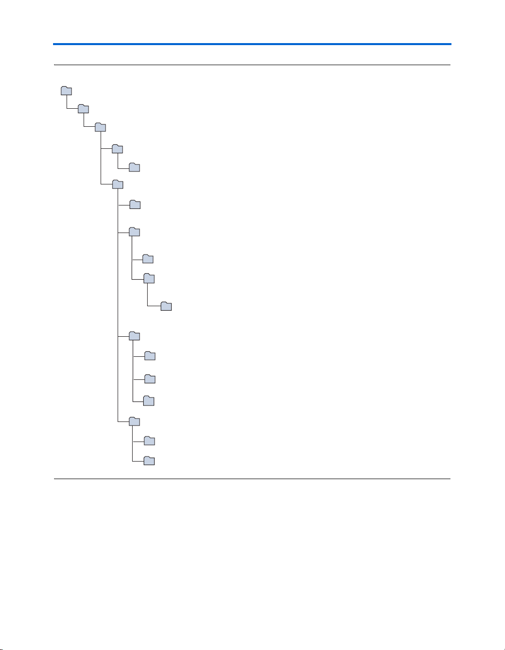
Figure 3 shows the directory structure after you install the PCI Compiler
User Guide, where <path> is the installation directory. The default
installation directory on Windows is c:\altera\<version>; on Linux it is
/opt/altera<version>.
Altera Corporation User Guide Version 11.1 17
October 2011
Page 30
Installation and Licensing
Figure 3. Directory Structure
<path>
Installation directory.
ip
Contains the Altera MegaCore IP Library and third-party IP cores.
altera
Contains the Altera MegaCore IP Library.
common
Contains shared components.
ip_toolbench
Contains common IP Toolbench files.
pci_compiler
Contains the PCI Compiler files.
const_files
Contains constraint files that include all necessary assignments to meet your PCI timing requirements for
all supported Altera device families and development kits.
lib
Contains encrypted lower-level design files and other support files.
On Linux systems, you must add this directory as a user library in the Quartus II software.
megawizard_flow
Contains the files that are specific for PCI Compiler with MegaWizard flow.
sopc_flow
Contains the files that are specific for PCI Compiler with SOPC Builder.
ip_toolbench
Contains the necessary files for the parameterization wizard.
sopc_builder
Contains the necessary files for the SOPC Builder GUI. For Linux, this directory must be
added to the Component/Kit Library search path by choosing SOPC Builder Setup (File menu).
inc
Contains a header file that can be used in PCI Compiler with SOPC Builder flow. The header
file contains macros to access control and status registers inside the PCI-Avalon bridge.
qexamples
Contains example Quartus II projects and simulation waveforms for each of the PCI MegaCore functions.
ref_designs
Contains reference designs for common functions implemented with the PCI MegaCore functions.
testbench
Contains Verilog HDL and VHDL testbenches for simulating designs.
example
Contains example Quartus II projects using SOPC Builder.
testbench
Contains the Verilog HDL and VHDL testbenches for simulating designs that include the PCI-Avalon bridge.
18 User Guide Version 11.1 Altera Corporation
PCI Compiler October 2011
Page 31

About PCI Compiler
OpenCore Plus Evaluation
With Altera’s free OpenCore Plus evaluation feature, you can perform the
following actions:
■ Simulate the behavior of a megafunction (Altera MegaCore function
or AMPP
■ Verify the functionality of your design, as well as evaluate its size
SM
megafunction) within your system.
and speed quickly and easily.
■ Generate time-limited device programming files for designs that
include megafunctions.
■ Program a device and verify your design in hardware.
You only need to purchase a license for the megafunction when you are
completely satisfied with its functionality and performance, and want to
take your design to production.
After you purchase a license for PCI Compiler MegaCore function, you
can request a license file from the Altera website at
www.altera.com/licensing and install it on your computer. When you
request a license file, Altera emails you a license.dat file. If you do not
have Internet access, contact your local Altera representative.
f For more information on OpenCore Plus hardware evaluation, refer to
AN 320: OpenCore Plus Evaluation of Megafunctions.
OpenCore Plus Time-Out Behavior
OpenCore Plus hardware evaluation supports the following two
operation modes:
■ Untethered—the design runs for a limited time.
■ Tethered—requires a connection between your board and the host
computer. If tethered mode is supported by all megafunctions in a
design, the device can operate for a longer time or indefinitely.
All megafunctions in a device time out simultaneously when the most
restrictive evaluation time is reached. If there is more than one
megafunction in a design, a specific megafunction’s time-out behavior
may be masked by the time-out behavior of the other megafunctions.
1 For MegaCore functions, the untethered time-out is 1 hour; the
tethered time-out value is indefinite.
Your design stops working after the hardware evaluation time expires.
Altera Corporation User Guide Version 11.1 19
October 2011
Page 32

Installation and Licensing
20 User Guide Version 11.1 Altera Corporation
PCI Compiler October 2011
Page 33

Section I. PCI Compiler
With MegaWizard Plug-In
Manager Flow
The Altera PCI Compiler provides a complete solution for implementing
a conventional PCI interface using Altera devices. It contains the Altera
pci_mt64, pci_mt32, pci_t64, and pci_t32 MegaCore functions, a
Verilog HDL and VHDL testbench, and reference designs.
This section includes the following chapters:
■ Chapter 1, Getting Started
■ Chapter 2, Parameter Settings
■ Chapter 3, Functional Description
■ Chapter 4, Testbench
Altera Corporation Section I–1
October 2011
Page 34

PCI Compiler With MegaWizard Plug-In Manager Flow
Section I–2 User Guide Version 11.1 Altera Corporation
PCI Compiler October 2011
Page 35

1. Getting Started
Design Flow
To evaluate a PCI Compiler MegaCore function using the OpenCore Plus
feature include these steps in your design flow:
1. Obtain and install the PCI Compiler.
2. Create a custom variation of a PCI MegaCore function using
IP Toolbench.
1 IP Toolbench is a toolbar from which you can quickly and
easily view documentation, choose a PCI MegaCore
function , specify parameters, and generate all of the files
necessary for integrating the parameterized PCI MegaCore
function into your design.
3. Implement the rest of your system using the design entry method of
your choice.
4. Use the IP Toolbench-generated IP functional simulation model to
verify the operation of your design.
f For more information on IP functional simulation models,
refer to the Simulating Altera in Third-Party Simulation Tools
chapter in volume 3 of the Quartus II Handbook.
5. Use an Altera-provided PCI constraint file to meet the timing
requirements of the PCI specification.
f For more information on obtaining and using
Altera-provided PCI constraint files in your design, refer to
Appendix A, Using PCI Constraint File Tcl Scripts.
6. Use the Quartus II software to compile your design and perform
static timing analysis.
1 You can generate an OpenCore Plus time-limited
programming file, which you can use to verify the
operation of your design in hardware.
7. Purchase a license for the PCI Compiler.
Altera Corporation User Guide Version 11.1 1–1
October 2011
Page 36

PCI MegaCore Function Design Walkthrough
After you have purchased a license for the PCI Compiler, the design flow
involves the following additional steps:
1. Set up licensing.
2. Generate a programming file for the Altera device(s) on your board.
3. Program the Altera device(s) with the completed design.
4. Perform design verification.
PCI MegaCore
Function Design
Walkthrough
This walkthrough explains how to create a custom variation of a PCI
MegaCore function using the Altera PCI IP Toolbench and the Quartus II
software. When you finish generating a custom variation of the PCI
MegaCore function, you can incorporate it into your overall project.
This walkthrough explains how to create a custom variation of the
pci_mt64 MegaCore function in Verilog HDL. You can also use these
procedures for the pci_mt32, pci_t32 and pci_t64 MegaCore
functions, and substitute VHDL for Verilog HDL.
Altera recommends that you use the pci_mt32 MegaCore function for
32-bit applications. The pci_mt64 MegaCore function has additional
logic and I/O pins which are wasted if used in a 32-bit mode applications.
1 You can interface the pci_mt64 MegaCore function with 32-bit
agents on the bus. To operate in 32-bit mode only, connect an
input pin to the l_dis_64_extn signal. This signal disables the
64-bit extension signals if driven low.
This walkthrough consists of these steps:
■ Create a New Quartus II Project
■ Launch IP Toolbench
■ Step 1: Parameterize
■ Step 2: Set Up Simulation
■ Step 3: Generate
Create a New Quartus II Project
You need to create a new Quartus II project with the New Project Wizard,
which specifies the working directory for the project, assigns the project
name, and designates the name of the top-level design entity.
1–2 User Guide Version 11.1 Altera Corporation
PCI Compiler October 2011
Page 37

Getting Started
To create a new project, follow these steps:
1. Choose Programs > Altera > Quartus II <version> (Windows Start
menu) to run the Quartus II software. You can also use the
Quartus II Web Edition software.
2. Choose New Project Wizard (File menu).
3. Click Next in the New Project Wizard: Introduction (the
introduction does not display if you turned it off previously).
4. In the New Project Wizard: Directory, Name, Top-Level Entity
page, enter the following information:
a. Specify the working directory for your project. This
walkthrough uses the directory:
c:\altera\projects
b. Specify the name of the project. This walkthrough uses
pci_project for the project name.
1 The Quartus II software automatically specifies a top-level
design entity that has the same name as the project. Do not
change it.
5. Click Next to close this page and display the New Project Wizard:
Add Files page.
1 When you specify a directory that does not already exist, a
message asks if the specified directory should be created.
Click Yes to create the directory.
6. If you installed the MegaCore IP library in a different directory from
where you installed the Quartus II software, add user libraries by
following these steps on the New Project Wizard: Add Files page:
a. Click User Libraries.
b. Type <path>\pci_compiler\lib\ into the Library name box,
where <path> is the directory in which you installed the PCI
Compiler.
c. Click Add to add the path to the Quartus II project.
d. Click OK to save the library path in the project.
Altera Corporation User Guide Version 11.1 1–3
October 2011 PCI Compiler
Page 38

PCI MegaCore Function Design Walkthrough
7. Click Next to close this page and display the New Project Wizard:
Family & Device Settings page.
8. On the New Project Wizard: Family & Device Settings page,
choose the following:
● In the Family list, choose Stratix as the target device family.
● Under Target device, select a Specific device selected in the
‘Available devices’ list.
● Under Show in ‘Available device’ list, in the Speed Grade list,
choose Any.
● In the Available Devices list, select EP1S60F1020C5.
1 These procedures create a design targeting the Stratix
9. The remaining pages in the New Project Wizard are optional. Click
Finish to complete the Quartus II project.
You have finished creating your new Quartus II project.
Launch IP Toolbench
device family. You can also use these procedures for other
supported device families. MAX II devices are supported
by the pci_mt32 and pci_t32 MegaCore functions only.
To launch IP Toolbench in the Quartus II software, follow these steps:
1. Start the MegaWizard Plug-In Manager by choosing MegaWizard
Plug-In Manager (Tools menu). The MegaWizard Plug-In Manager
dialog box is displayed.
f For more information on MegaWizard Plug-in Manager,
refer to Quartus II Help.
2. Specify that you want to create a new custom megafunction
variation and click Next.
3. Under Installed Plug-Ins, expand the Interfaces>PCI folder, and
click on PCI to select the PCI Compiler v10.1.
4. Select the output file type for your design; the wizard supports
VHDL and Verilog HDL. For this walkthrough, choose Verilog
HDL.
1–4 User Guide Version 11.1 Altera Corporation
PCI Compiler October 2011
Page 39

Getting Started
5. The MegaWizard Plug-In Manager shows the project path that you
specified in the New Project Wizard. Append a variation name for
the MegaCore function output files using the format <project
path>\<variation name>. For this walkthrough, specify
c:\altera\projects for the directory name, and pci_project.v for the
output file variation name.
6. Click Next to launch IP Toolbench for the PCI Compiler.
Step 1: Parameterize
To parameterize your MegaCore function, follow these steps:
1. Click Step 1: Parameterize in IP Toolbench to open the
Parameterize - PCI Compiler dialog box.
f For more information on the parameters you set during
this walkthrough, refer to Chapter 2, Parameter Settings.
2. On the PCI MegaCore Function Settings page, select the following
options:
a. Under Te c hn o l o g y, select PCI.
b. Under Application Speed, turn on PCI 66-MHz Capable.
c. Select the desired PCI MegaCore function in the PCI MegaCore
section. For this walkthrough select 64-Bit Master/Target
(pci_mt64).
3. Click Next to open the Read-Only PCI Configuration Registers
page. You can modify the values of the read-only PCI configuration
registers on this page. For this walkthrough, use the default settings.
Altera Corporation User Guide Version 11.1 1–5
October 2011 PCI Compiler
Page 40

PCI MegaCore Function Design Walkthrough
4. Click Next to open the Base Address Registers (BARs) page. This
page allows you to configure the PCI base address registers (BARs)
that define the address ranges of Memory and I/O write and read
requests that your application will claim for the PCI interface.
For this walkthrough, specify these settings:
a. Ensure that Implement Only 32 Bit BARs is selected under
32/64 Bit BARs.
b. Click BAR0 = 1 MBytes (Memory).
c. A window showing default settings for BAR0 displays. For this
walkthrough, use the default sliding pointer setting so that
BAR0 reserves 1 MByte (0xFFF00000) of memory.
d. Click OK.
e. Click BAR1 .
f. A window showing the default settings for BAR1 displays.
Turn o n Enable.
g. Select I/O for the type of memory reserved.
h. Move the sliding pointer so that BAR1 reserves 64 Bytes
(0xFFFFFFC1) of I/O memory.
i. Click OK.
j. Select BAR2 Unused: Click to Configure.
k. A window showing default settings of BAR2 displays. Turn on
Enable.
l. Move the sliding pointer so that BAR2 reserves 1 MByte
(0xFFF00000) of memory.
m. Click OK.
5. Click Next to open the Advanced PCI MegaCore Features page. For
this walkthrough, use the default settings for all options on this
page.
6. Click Finish to complete the parameterization of your pci_mt64
MegaCore function variation.
1–6 User Guide Version 11.1 Altera Corporation
PCI Compiler October 2011
Page 41

Getting Started
Step 2: Set Up Simulation
An IP functional simulation model is a cycle-accurate VHDL or Verilog
HDL model file produced by the Quartus II software. The model allows
for fast functional simulation of IP using industry-standard VHDL and
Verilog HDL simulators.
c Only use these simulation model output files for simulation
purposes and expressly not for synthesis or any other purposes.
Using these models for synthesis creates a nonfunctional design.
1 Some third-party synthesis tools can use a netlist that contains
only the structure of the MegaCore function, but not detailed
logic, to optimize performance of the design that contains the
MegaCore function. If your synthesis tool supports this feature,
turn on Generate netlist.
To generate an IP functional simulation model for your MegaCore
function, follow these steps:
1. Click Step 2: Set Up Simulation in IP Toolbench.
2. Turn on Generate Simulation Model.
3. Choose Verilog HDL in the Language list.
4. Click OK.
Step 3: Generate
Generate your MegaCore function after specifying parameter values and
IP functional simulation model options.
1 Clicking Quartus II Constraints displays up-to-date
information about PCI Constraint files.
f For more information on PCI constraint files, refer to Appendix A, Using
PCI Constraint File Tcl Scripts.
Altera Corporation User Guide Version 11.1 1–7
October 2011 PCI Compiler
Page 42

PCI MegaCore Function Design Walkthrough
To generate your MegaCore function, follow these steps:
1. Click Step 3: Generate in IP Toolbench. A summary of files
generated to your project directory is displayed.
Table 1–1 describes the generated files and other files that may be in
your project directory. The names and types of files specified in the
IP Toolbench report vary based on whether you created your design
with VHDL or Verilog HDL.
Table 1–1. IP Toolbench-Generated Files
Extension Description
<variation name>.v or .vhd A MegaCore function variation file that defines a VHDL or Verilog HDL
<variation name>_bb.v A Verilog HDL black box file for the MegaCore function variation. Use this
<variation name>.bsf A Quartus II symbol file for the MegaCore function variation. You can use
<variation name>.qip Contains Quartus II project information for your MegaCore function
<variation name>_syn.v A timing and resource estimation netlist for use in some third-party
<variation name>.ppf This XML file describes the MegaCore pin attributes to the Quartus II Pin
<variation name>.vo or .vho A Verilog HDL or VHDL IP functional simulation model.
pci_constraints_for_<variation
name>.tcl
<variation name>_nativelink.tcl A tcl script for assigning NativeLink simulation testbench settings to the
<variation name>.html A MegaCore function report file.
top-level description of the custom MegaCore function. Instantiate the
entity defined by this file inside of your design. Include this file when
compiling your design in the Quartus II software.
file when using a third-party EDA tool to synthesize your design.
this file in the Quartus II block diagram editor.
variations.
synthesis tools. This file is generated when the option Generate netlist on
the EDA page is turned on.
Planner. MegaCore pin attributes include pin direction, location, I/O
standard assignments, and drive strength. If you launch IP Toolbench
outside of the Pin Planner application, you must explicitly load this file to
use Pin Planner.
A tcl script for assigning timing constraints to the MegaCore function.
Quartus project.
1–8 User Guide Version 11.1 Altera Corporation
PCI Compiler October 2011
Page 43

Getting Started
2. After you review the generation report, click Exit to close IP
To ol be n ch .
1 If you generate the MegaCore function instance in a Quartus II
project, you are prompted to add the Quartus II IP File (.qip)
files to the current Quartus II project. The .qip file is generated
by the MegaWizard interface, and contains information about
the generated IP core. In most cases, the .qip file contains all of
the necessary assignments and information required to process
the MegaCore function or system in the Quartus II compiler. The
MegaWizard interface generates a single .qip file for each
MegaCore function.
You can now integrate your PCI MegaCore function variation into your
design and compile.
Simulate the Design
To simulate your design, you use the IP functional simulation models
generated by IP Toolbench in conjunction with the Altera-provided
PCI testbench. The IP functional simulation model is the .vo or .vho file
generated as specified in “Step 2: Set Up Simulation” on page 1–7. These
files are generated in the directory you specified in the MegaWizard PlugIn Manager. Compile this IP functional simulation model in your
simulation environment as instructed below to perform functional
simulation of your PCI MegaCore function variation.
Altera Corporation User Guide Version 11.1 1–9
October 2011 PCI Compiler
Page 44

Simulate the Design
This section of the walkthrough uses the following:
■ The IP toolbench-generated PCI testbench in the
c:\altera\projects\pci_project_nativelink\verilog\pci_mt64
directory
■ The IP functional simulation model generated as specified in “Step
2: Set Up Simulation” on page 1–7
■ The ModelSim
■ The generated NativeLink script in the project directory,
®
software
c:\altera\projects
For this walkthrough, follow these steps:
1. On the EDA Tool Option page in the Quartus II software (To ol s >
Options > EDA Tools Option), set the location of the ModelSim
executable .
1 If you are using other simulators, set the location of your
preferred EDA simulation tool executable. This is a global
setting, and needs to be done only once.
2. At the Quartus II Tcl Console, run the following command:
source pci_top_nativelink.tcl
3. On the Simulation page (Assignments > EDA Tools Settings >
Simulation), do the following:
● select ModelSim from the Too l N a me list
● select Compile test bench under NativeLink settings.
4. Perform analysis and synthesis to create the required netlist.
5. Run the simulation.
f For more information on simulation using NativeLink, refer to
Simulating Altera IP in Third-Party Simulation Tools chapter in volume 3 of
the Quartus II Handbook.
1–10 User Guide Version 11.1 Altera Corporation
PCI Compiler October 2011
Page 45

Getting Started
Simulation in the Quartus II Software
Altera provides Vector Waveform Files (.vwf) for each of the PCI
MegaCore functions to perform functional simulation in the Quartus II
software. The .vwf files are provided in the subdirectories at <path>\
pci_compiler\megawizard_flow\qexamples\<PCI MegaCore
function>\sim. For an explanation of the provided .vwf files, refer to “The
Quartus II Simulation Files” on page 1–12.
This user guide explains the behavior and usage of the PCI MegaCore
functions for the most common PCI transactions. You can use the .vwf
files to further understand the local-side behavior of a PCI MegaCore
function for different PCI bus conditions. In addition, you can modify the
provided .vwf files to simulate other scenarios of interest.
1 This procedure demonstrates functional simulation in the
Quartus II software of a pci_mt64 MegaCore function
variation. You can also use this procedure for the pci_mt32,
pci_t32 and pci_t64 MegaCore functions.
To perform functional simulation in the Quartus II software, perform
these steps:
1. Go to the <path>\pci_compiler\megawizard_flow\
qexamples\pci_mt64 directory.
2. Open the Quartus II project by double-clicking on pci_top.qpf.
1 This Quartus II project contains a PCI MegaCore function
variation with the parameter settings required to simulate
the included .vwf files successfully. For a description of the
parameter settings required to simulate the included .vwf
files, refer to “The Quartus II Simulation Files” on
page 1–12.
3. Choose Generate Functional Simulation Netlist (Processing
menu).
The Quartus II software may issue several warning messages,
including messages indicating that one or more registers are stuck at
ground. These warning messages are due to parameter settings and
can be ignored.
4. After compilation has finished successfully, choose Simulator Too l
(Processing Menu).
5. In the Simulation mode list, select Functional.
Altera Corporation User Guide Version 11.1 1–11
October 2011 PCI Compiler
Page 46

The Quartus II Simulation Files
6. In the Simulation input, specify <path>\pci_compiler\
7. Click Start to start the simulation.
8. Click Report to view the simulation results.
megawizard_flow\qexamples\pci_mt64\sim\target\
cfg_wr_rd.vwf.
The Quartus II
Simulation Files
This section contains information about the Quartus II simulation files
supplied with the pci_mt64, pci_mt32, pci_t64, and pci_t32
MegaCore functions. These simulation files are provided in .vwf format.
You can use these simulation files to further understand the local-side
behavior of the PCI MegaCore functions for different PCI bus conditions.
In addition, you can modify the simulation files to simulate the scenarios
of interest.
The simulation files are based on the parameter settings used in pci_top.v.
There is a separate pci_top.v file for each of the four MegaCore functions.
The files are located in <path>\pci_compiler\
megawizard_flow\qexamples\<PCI MegaCore function>. This example
design file implements 6 base address registers (BARs), and an expansion
ROM BAR, with the following attributes:
■ BAR0 reserving 256 Megabytes (MBytes) (memory)
■ BAR1 reserving 64 Bytes (I/O)
■ BAR2 reserving 16 MBytes (memory)
■ BAR3 reserving 1 MByte (memory)
■ BAR4 reserving 64 Kilobytes (KBytes) (memory)
■ BAR5 reserving 4 KBytes (memory)
■ Expansion ROM BAR reserving 1 MByte (memory)
The simulation files contain functional simulation waveforms and should
be used after choosing Generate Functional Simulation Netlist
(Processing menu) for your design.
For more information regarding simulating with .vwf files, refer to
“Simulation in the Quartus II Software” on page 1–11.
The following sections describe the simulation files provided with the
PCI Compiler.
1–12 User Guide Version 11.1 Altera Corporation
PCI Compiler October 2011
Page 47

Master Simulation Files
Table 1–2 describes the Quartus II simulation files included in the
<path>\pci_compiler\megawizard_flow\qexamples\
pci_mt64\sim\master directory.
Table 1–2. pci_mt64 Master Simulation Files
Simulation File Name Description
Master Read
mmbr64
mmbr32_64
mmbr32_32
mmsr64
mmsr32_32
mmbr64_mabrt
mmbr64_tabrt
mmbr64_tdisc_wd
mmbr64_tdisc_wod
mmbr64_tret
mmbr64_lte
mior
mcfgr
mmbw64
mmbw32_64
mmbw32_32
mmsw32_32
mmbw64_mabrt
mmbw64_tabrt
mmbw64_tdisc_wd
mmbw64_tdisc_wod
mmbw64_tret
mmbw64_lte
miow
mcfgw
Memory Burst Read, 64-Bit PCI, 64-Bit Local
Memory Burst Read, 32-Bit PCI, 64-Bit Local
Memory Burst Read, 32-Bit PCI, 32-Bit Local
Memory Single-Cycle, 64-Bit PCI, 64-Bit Local
Memory Single-Cycle, 32-Bit PCI, 32-Bit Local
Master Abort, 64-Bit PCI, 64-Bit Local
Target Abort Response, 64-Bit PCI, 64-Bit Local
Target Disconnect with Data Response, 64-Bit PCI, 64-Bit Local
Target Disconnect without Data Response, 64-Bit PCI, 64-Bit Local
Target Retry Response, 64-Bit PCI, 64-Bit Local
Latency Timer Expires, 64-Bit PCI, 64-Bit Local
I/O Read
Configuration Read
Master Write
Memory Burst Write, 64-Bit PCI, 64-Bit Local
Memory Burst Write, 32-Bit PCI, 64-Bit Local
Memory Burst Write, 32-Bit PCI, 64-Bit Local
Memory Single-Cycle, 32-Bit PCI, 32-Bit Local
Master Abort, 64-Bit PCI, 64-Bit Local
Target Abort Response, 64-Bit PCI, 64-Bit Local
Target Disconnect with Data Response, 64-Bit PCI, 64-Bit Local
Target Disconnect without Data Response, 64-Bit PCI, 64-Bit Local
Target Retry Response, 64-Bit PCI, 64-Bit Local
Latency Timer Expires, 64-Bit PCI, 64-Bit Local
I/O Write
Configuration Write
Getting Started
Altera Corporation User Guide Version 11.1 1–13
October 2011 PCI Compiler
Page 48

The Quartus II Simulation Files
Table 1–3 describes the Quartus II simulation files included in the
<path>\pci_compiler\megawizard_flow\qexamples\
pci_mt32\sim\master directory.
Table 1–3. pci_mt32 Master Simulation Files
Simulation File
Name
mmbr
mmsr
mmbr_mabrt
mmbr_tabrt
mmbr_tdisc_wd
mmbr_tdisc_wod
mmbr_tret
mmbr_lte
mior
mcfgr
mmbw
mmsw
mmbw_mabrt
mmbw_tabrt
mmbw_tdisc_wd
mmbw_tdisc_wod
mmbw_tret
mmbw_lte
miow
mcfgw
Description
Master Read
Memory Burst Read
Memory Single-Cycle
Master Abort
Target Abort Response
Target Disconnect with Data Response
Target Disconnect without Data Response
Target Retry Response
Latency Timer Expires
I/O Read
Configuration Read
Master Write
Memory Burst Write
Memory Single-Cycle
Master Abort
Target Abort Response
Target Disconnect with Data Response
Target Disconnect without Data Response
Target Retry Response
Latency Timer Expires
I/O Write
Configuration Write
1–14 User Guide Version 11.1 Altera Corporation
PCI Compiler October 2011
Page 49

Target Simulation Files
Table 1–4 describes the Quartus II simulation files included in the
<path>\pci_compiler\megawizard_flow\qexamples\
<pci_mt64 or pci_t64>\sim\target directory.
Table 1–4. pci_mt64 & pci_t64 Target Simulation Files
Simulation File Name Description
Target Read
tmbr64
tmbr32_64
tmsr64
tmbr64_abrt
tmbr64_disc_wd
tmbr64_disc_wod
tmbr64_ret
cfg_wr_rd
tior
exp_rom_tmbr64
tmbw64
tmbw32_64
tmsw64
tmbw64_abrt
tmbw64_disc_wd
tmbw64_disc_wod
tmbw64_ret
tiow
exp_rom_tmbw64
Memory Burst Read, 64-Bit PCI, 64-Bit Local
Memory Burst Read, 32-Bit PCI, 64-Bit Local
Memory Single-Cycle, 64-Bit PCI, 64-Bit Local
Memory Abort, 64-Bit PCI, 64-Bit Local
Memory Disconnect with Data, 64-Bit PCI, 64-Bit Local
Memory Disconnect without Data, 64-Bit PCI, 64-Bit Local
Memory Retry, 64-Bit PCI, 64-Bit Local
Configuration Write and Read
I/O Read
Expansion ROM Memory Burst Read, 64-Bit PCI, 64-Bit Local
Target Write
Memory Burst Write, 64-Bit PCI, 64-Bit Local
Memory Burst Write, 32-Bit PCI, 64-Bit Local
Memory Single-Cycle, 64-Bit PCI, 64-Bit Local
Memory Abort, 64-Bit PCI, 64-Bit Local
Memory Disconnect with Data, 64-Bit PCI, 64-Bit Local
Memory Disconnect without Data, 64-Bit PCI, 64-Bit Local
Memory Retry, 64-Bit PCI, 64-Bit Local
I/O Write
Expansion ROM Memory Burst Write, 64-Bit PCI, 64-Bit Local
Getting Started
Altera Corporation User Guide Version 11.1 1–15
October 2011 PCI Compiler
Page 50

Compile the Design
Table 1–5 describes the Quartus II simulation files included in the
<path>\pci_compiler\megawizard_flow\qexamples\
<pci_mt32 or pci_t32>\sim\target directory.
Table 1–5. pci_mt32 & pci_t32 Target Directory
Simulation File
Name
tmbr
tmsr
tmbr_abrt
tmbr_disc_wd
tmbr_disc_wod
tmbr_ret
cfg_wr_rd
tior
exp_rom_tmbr
tmbw
tmsw
tmbw_abrt
tmbw_disc_wd
tmbw_disc_wod
tmbw_ret
tiow
exp_rom_tmbw
Description
Target Read
Memory Burst Read
Memory Single-Cycle
Memory Abort
Memory Disconnect with Data
Memory Disconnect without Data
Memory Retry
Configuration Write and Read
I/O Read
Expansion ROM Memory Burst Read
Target Write
Memory Burst Write
Memory Single-Cycle
Memory Abort
Memory Disconnect with Data
Memory Disconnect without Data
Memory Retry
I/O Write
Expansion ROM Memory Burst Write
Compile the
Design
You can use the Quartus II software to compile your design.
Altera provides constraint files to ensure that the PCI MegaCore function
achieves PCI specification timing requirements in Altera devices. This
walkthrough incorporates a constraint file included with PCI Compiler.
f For more information on using Altera-provided constraint files in your
design, refer to Appendix A, Using PCI Constraint File Tcl Scripts.
For instructions on compiling your design, refer to Quartus II Help.
1–16 User Guide Version 11.1 Altera Corporation
PCI Compiler October 2011
Page 51

Getting Started
For this walkthrough, follow these steps:
1. Open <path>\pci_example\pci_top.qpf (the pci_top project) in the
Quartus II software.
1 This is the same project you created in “PCI MegaCore
Function Design Walkthrough” on page 1–2.
2. Choose Utility Windows > Tcl Console (View menu).
3. Source the generated constraint file by typing the following
commands at the Quartus II Tcl Console command prompt:
source pci_constraints_for_pci_top.tcl r
add_pci_constraints r
1 The constraint file uses the following naming convention:
pci_constraints_for_<variation name>.tcl.
4. Monitor the Quartus II Tcl Console to see the actions performed by
the script.
To verify the PCI timing assignments in your project, perform the
following steps:
1. Choose Start Compilation (Processing menu) in the Quartus II
software.
2. After compilation, expand the Timing Analyzer folder in the
Compilation Report by clicking the + icon next to the folder name.
Note the values in the Clock Setup, tsu, th, and tco report sections.
Altera Corporation User Guide Version 11.1 1–17
October 2011 PCI Compiler
Page 52

Program a Device
Program a
Device
PCI Timing Support
After you have compiled your design, program your targeted Altera
device and verify your design in hardware.
With Altera's free OpenCore Plus evaluation feature, you can evaluate the
PCI MegaCore function before you purchase a license. OpenCore Plus
evaluation allows you to generate an IP functional simulation model and
produce a time-limited programming file.
You can simulate the PCI Compiler MegaCore function in your design
and perform a time-limited evaluation of your design in hardware.
f For more information on IP functional simulation models, refer to the
Simulating Altera in Third-Party Simulation Tools chapter in volume 3 of
the Quartus II Handbook.
For more information on OpenCore Plus hardware evaluation using the
PCI MegaCore functions, refer to “Compliance Summary” on page 10
and AN 320: OpenCore Plus Evaluation of Megafunctions.
For more information on setting up licensing for PCI Compiler, refer to
“PCI Timing Support” on page 1–18.
Designs that use an Altera PCI Compiler MegaCore function must use an
Altera-provided PCI constraint file. A PCI constraint file does the
following:
■ Constrains Quartus II compilations so that your design meets PCI
timing requirements
■ Specifies the required PCI pin assignments for your board layout
The PCI Compiler generates PCI constraint files in the form of Tcl scripts
that allow you to meet the PCI timing requirements in the Quartus II
software.
The constraint files use the following naming convention:
pci_constraints_for_<variation name>.tcl
These constraint files have been tested against PCI Compiler 11.1 and
Quartus II 11.1 and meet PCI Compiler timing.
To use the constraint file, follow these steps:
1. Open your project in the Quartus II software.
1–18 User Guide Version 11.1 Altera Corporation
PCI Compiler October 2011
Page 53

Getting Started
2. In the Quartus II software, choose Tcl Co ns o le (View > Utility
Windows menu).
3. To source the constraint file, type the following in the Quartus II Tcl
console:
source pci_constraints_for_<variation name>.tcl
add_pci_constraints [-speed "33" | "66"]
[-no_compile] [no_pinouts] [-help]
f For more information on PCI Compiler constraint files, refer to
Appendix A, Using PCI Constraint File Tcl Scripts.
Using the Reference Designs
The following sections outline how to use the reference designs that are
packaged with the PCI Compiler
pci_mt32 MegaCore Function Reference Design
The pci_mt32 MegaCore Function Reference Design example illustrates
how to interface local logic to the pci_mt32 MegaCore function. The
reference design includes a target and a master interface to the pci_mt32
function and the SDRAM memory. The DMA engine is implemented in
the local logic to enable the pci_mt32 function to operate as a bus master.
The design implements a FIFO interface to solve latency issues when data
is transferred between the PCI bus and the SDRAM.
The pci_mt32 MegaCore Function Reference Design requires the Quartus
II software.
Table 1–6 describes the directory structure of the pci_mt32 MegaCore
Function Reference Design. The directory names are relative to the
following path:
<path>/pci_compiler/megawizard_flow
/ref_designs/ref_designs/pci_mt32/vhdl
where <path> is the directory in which you installed the PCI Compiler.
Altera Corporation User Guide Version 11.1 1–19
October 2011 PCI Compiler
Page 54

Using the Reference Designs
Refer to Tab le 1 –3 the pci_mt32 MegaCore Function Reference Design
Directory Structure for more details regarding the directory structure.
Table 1–6. Directory Structure of pci_mt32 MegaCore Reference Design
Directory Name Description
chip_top This directory contains a top-level design file that
instantiates the following modules:
● pci_mt32 MegaCore function variation file
● Local interface logic
● SDR SDRAM interface
● SDR SDRAM controller
pci_top This directory contains a pci_mt32 MegaCore function top-
level wrapper file. This wrapper file was generated using IP
Toolbench with the following parameters selected using the
Parameterize - PCI Compiler Wizard:
● BAR0 reserves 1MB of memory space
● BAR1 reserves 32MB of memory space
pci_local This directory contains local interface logic files. For more
information on these files, refer to FS 12: pci_mt32
MegaCore Function Reference Design.
sdr_intf This directory contains files for the interface logic between
the PCI local interface logic and the SDR SDRAM controller.
sdr_cntrl This directory contains files for the SDR SDRAM controller.
Synthesis & Compilation Instructions
To compile the pci_mt32 MegaCore Function Reference Design in the
Quartus II software, perform the following steps:
1. Create a new project in the Quartus II software, specifying
<path>/pci_compiler/megawizard_flow/
ref_designs/pci_mt32/vhdl/chip_top.vhd as the top-level
design file.
2. Add the following directories as user libraries in the Quartus II
software:
<path>/pci_compiler/lib
<path>/pci_compiler/megawizard_flow/
ref_designs/pci_mt32/vhdl/chip_top
<path>/pci_compiler/megawizard_flow
/ref_designs/pci_mt32/vhdl/pci_local
1–20 User Guide Version 11.1 Altera Corporation
PCI Compiler October 2011
Page 55

Getting Started
<path>/pci_compiler/megawizard_flow
/ref_designs/pci_mt32/vhdl/sdr_intf
<path>/pci_compiler/megawizard_flow
/ref_designs/pci_mt32/vhdl/sdr_cntrl
f Refer to Quartus II help for information on how to add
user libraries in the Quartus II software.
3. Include the following files in your Quartus II project:
<path>/pci_compiler/megawizard_flow
/ref_designs/pci_mt32/vhdl/chip_top
/vhdl_components.vhd
<path>/pci_compiler/megawizard_flow
/ref_designs/pci_mt32/vhdl/pci_top/pci_top.vhd
4. Select the appropriate Altera device for your project.
Use an Altera-provided PCI constraint file.
f For more information on using PCI constraint files, refer to
Appendix A, Using PCI Constraint File Tcl Scripts.
5. Compile your project.
pci_mt64 MegaCore Function Reference Design
The pci_mt64 MegaCore Function Reference Design is an example that
shows how to connect the local-side signals of the Altera pci_mt64
MegaCore function to local-side applications when the MegaCore
function is used as a master or target on the PCI bus. The reference design
consists of the following elements:
■ Master control logic
■ Target control logic
■ DMA engine
■ Data path FIFO buffer functions
■ SDRAM interface
The pci_mt64 MegaCore Function Reference Design requires the Quartus
II software.
Table 1–7 describes the directory structure of the pci_mt64 MegaCore
Function Reference Design. The directory names are relative to the
following path:
Altera Corporation User Guide Version 11.1 1–21
October 2011 PCI Compiler
Page 56

Using the Reference Designs
<path>/pci_compiler/megawizard_flow
/ref_designs/pci_mt64/vhdl
where <path> is the directory in which you installed the PCI Compiler.
Table 1–7. Directory Structure of pci_mt64 MegaCore Reference Design
Directory Name Description
chip_top This directory contains a top-level design file that
instantiates the following modules:
● pci_mt64 MegaCore function variation file
● Local interface logic
● SDR SDRAM interface
● SDR SDRAM controller
pci_top This directory contains a pci_mt64 MegaCore function top-
level wrapper file. This wrapper file was generated using IP
Toolbench with the following parameters selected using the
Parameterize - PCI Compiler Wizard:
● BAR0 reserves 1MB of memory space
● BAR1 reserves 32MB of memory space
pci_local This directory contains local interface logic files. For more
information on these files, refer to FS 10: pci_mt64
MegaCore Function Reference Design.
sdr_intf This directory contains files for the interface logic between
the PCI local interface logic and the SDR SDRAM controller.
sdr_cntrl This directory contains files for the SDR SDRAM controller.
synthesis & Compilation Instructions
To compile the pci_mt64 MegaCore Function Reference Design in the
Quartus II software, follow these steps:
1. Create a new project in the Quartus II software, specifying the toplevel design file as follows:
<path>/pci_compilerv/megawizard_flow
/ref_designs/pci_mt64/vhdl/chip_top.vhd
2. Add the following directories as user libraries in the Quartus II
software:
<path>/pci_compiler/lib
<path>/pci_compiler/megawizard_flow
/ref_designs/pci_mt64/vhdl/chip_top
1–22 User Guide Version 11.1 Altera Corporation
PCI Compiler October 2011
Page 57

Getting Started
<path>/pci_compiler/megawizard_flow
/ref_designs/pci_mt64/vhdl/pci_local
<path>/pci_compiler/megawizard_flow
/ref_designs/pci_mt64/vhdl/sdr_intf
<path>/pci_compiler/megawizard_flow
/ref_designs/pci_mt64/vhdl/sdr_cntrl
f Refer to Quartus II help for information on how to add
user libraries in the Quartus II software.
3. Include the following files in your Quartus II project:
<path>/pci_compiler/megawizard_flow
/ref_designs/pci_mt64/vhdl/chip_top
/vhdl_components.vhd
<path>/pci_compiler/megawizard_flow
/ref_designs/pci_mt64/vhdl/pci_top/pci_top.vhd
4. Select the appropriate Altera device for your project.
5. Use an Altera-provided PCI constraint file for the device you have
selected.
f For more information on using PCI constraint files, refer to
Appendix A, Using PCI Constraint File Tcl Scripts.
6. Compile your project.
Altera Corporation User Guide Version 11.1 1–23
October 2011 PCI Compiler
Page 58

Using the Reference Designs
1–24 User Guide Version 11.1 Altera Corporation
PCI Compiler October 2011
Page 59

2. Parameter Settings
This chapter describes the parameters available to configure PCI
Compiler, including:
■ “PCI MegaCore Function Settings”
■ “Read-Only PCI Configuration Registers”
■ “PCI Base Address Registers (BARs)”
■ “Advanced PCI MegaCore Function Features”
■ “Variation File Parameters”
Parameterize PCI Compiler
PCI MegaCore Function Settings
You can customize the PCI MegaCore functions by changing parameters
and specifying optional features using the Parameterize - PCI Compiler
wizard. Start the wizard by clicking Step 1: Parameterize in IP Toolbench.
These parameters allow you to customize the PCI MegaCore functions to
meet specific application requirements, such as defining read-only and
read/write PCI configuration space. The wizard is also used to enable
and parameterize optional features.
For a complete list of parameter names and descriptions found in a
generated PCI MegaCore function variation file, refer to “Variation File
Parameters” on page 2–7.
The PCI MegaCore functions are capable of operating at clock speeds of
up to 66 MHz. Depending on the PCI device speed, the PCI 66-MHz
Capable option is enabled or disabled on the PCI MegaCore Function
Settings page of the Parameterize - PCI Compiler wizard.
When turned on, the PCI 66-MHz Capable option sets bit 5 of the PCI
configuration space status register. For more information on the function
of this register, refer to “Configuration Registers” on page 3–28.
Altera Corporation User Guide Version 11.1 2–1
October 2011
Page 60

Read-Only PCI Configuration Registers
Read-Only PCI
Configuration
Registers
PCI Base Address Registers (BARs)
Parameters for read-only PCI configuration space registers are defined on
the Read-Only PCI Configuration Registers page of the Parameterize -
PCI Compiler wizard.
The following read-only PCI configuration space register parameters are
set on this page:
■ Device ID
■ Ven do r I D
■ Revision ID
■ Subsystem ID
■ Subsystem Vendor ID
■ Minimum Grant
■ Maximum Latency
■ Class Code
The parameters require hexadecimal values. For information on the
functionality of the read-only registers, refer to “Configuration Registers”
on page 3–28.
The PCI MegaCore functions implement up to six 32-bit BARs and an
expansion ROM BAR. The pci_mt64 and pci_t64 MegaCore functions
can also implement one 64-bit BAR using either BAR 1 and BAR0, or
BAR2 and BAR1.
You must instantiate at least one BAR in your application design.
Multiple BARs must be implemented in sequence starting from BAR0. By
default, BAR0 is enabled and reserves 1 MByte of memory space.
In addition to allowing normal BAR operation where the system writes
the base address value during system initialization, the PCI MegaCore
functions allow the base address of any BAR to be hardwired using the
Hardwire BAR option. When hardwiring a BAR, the BAR address
becomes a read-only value supplied to the PCI MegaCore function
through the parameter value. System software cannot overwrite a base
address register that is hardwired. The value provided for the hardwired
BAR is written into the BAR, including the four least significant bits.
Thus, you must provide the appropriate value for all of the contents of the
BAR.
1 Use hardwired BARs in closed systems only.
The PCI BAR attributes are defined on the Base Address Registers
(BARs) page of the Parameterize - PCI Compiler wizard.
2–2 User Guide Version 11.1 Altera Corporation
PCI Compiler October 2011
Page 61

Parameter Settings
The pci_mt64 and pci_t64 MegaCore functions allow the
implementation of 64-bit BARs. When implementing a 64-bit BAR, most
systems do not require that all of the upper bits be decoded. The PCI
MegaCore functions allow the number of read/write bits on the upper
BAR to be defined for specific application needs. For example, if the
maximum size of memory in your system is 512 Gigabytes (GBytes), you
only need 8 bits of the most significant BAR to be decoded. The
acceptable range of read/write bits is between 8 and 32. When the
maximum number of read/write bits is set to 32, all bits of the most
significant BAR will be decoded.
For more information on the function of BARs, refer to “Base Address
Registers” on page 3–37.
Advanced PCI MegaCore Function Features
Optional registers, interrupt capabilities, and optional master features are
set on the Advanced PCI MegaCore Function Features page of the
Parameterize - PCI Compiler wizard.
Optional Registers
The PCI MegaCore functions support two optional read-only registers:
the capabilities list pointer register and CIS cardbus pointer register.
When these features are used, the values provided in the wizard are
stored in these optional registers. When CompactPCI technology is
selected on the initial page of the wizard, the capabilities list pointer
register on the Advanced PCI MegaCore Function Features page is
automatically turned on with the default value of 0x40.
Altera Corporation User Guide Version 11.1 2–3
October 2011
Page 62

Advanced PCI MegaCore Function Features
Optional Interrupt Capabilities
The PCI MegaCore functions support optional PCI interrupt capabilities.
For example, if an application uses the interrupt pin, the interrupt pin
register indicates that the interrupt signal (intan) is used by storing a
value of 0x01 in the interrupt pin register. Turning off Use Interrupt Pin
on the Advanced PCI MegaCore Function Features page results in the
interrupt pin register being set to 0x00.
The PCI MegaCore functions also include an option to respond to the
interrupt acknowledge command. If Support Interrupt Acknowledge
Command is turned off, the PCI MegaCore function ignores the interrupt
acknowledge command. When Support Interrupt Acknowledge
Command is turned on, the PCI MegaCore function responds to the
interrupt acknowledge command by treating it as a regular target
memory read. The local side must implement the logic necessary to
respond to the interrupt acknowledge command.
For more information on the capabilities list pointer, CIS cardbus pointer,
and interrupt pin registers, refer to “Configuration Registers” on
page 3–28.
Master Features
The pci_mt64 and pci_mt32 MegaCore functions also provide the
following options available in the Parameterize - PCI Compiler wizard:
■ Allow Variable Byte Enables During Burst Transactions
■ Use in Host Bridge Application
■ Allow Internal Arbitration Logic
■ Disable Master Latency Timer
■ Assume ack64n Response
Enable these features on the Advanced PCI MegaCore Function Features
page as described in the following sections.
2–4 User Guide Version 11.1 Altera Corporation
PCI Compiler October 2011
Page 63

Parameter Settings
Allow Variable Byte Enables During Burst Transactions
In a default master burst transaction the byte enables accompanying the
initial data word provided by the local side are used throughout the
master burst transaction. Turning on Allow Variable Byte Enables
During Burst Transactions allows byte enables to change for successive
data words during the transaction. This option affects both burst memory
read and burst memory write master transactions. However, use this
option only for burst memory write master transactions. Refer to “Burst
Memory Write Master Transaction with PCI Wait State” on page 3–117 for
more information. For burst memory read master transactions, you must
keep the byte enables constant throughout the transaction. Typically the
byte enable values are set to 0x00 for burst memory read master
transactions.
Use in Host Bridge Application
Turning on the Use in Host Bridge Application option allows you to
implement a host bridge design using the pci_mt64 and pci_mt32
MegaCore functions. For more information on using the pci_mt64 or
pci_mt32 MegaCore functions in a host bridge application, refer to
“Host Bridge Operation” on page 3–127.
Allow Internal Arbitration Logic
Many designs that utilize the pci_mt64 or pci_mt32 MegaCore
functions as a host bridge implement other central resource functionality
in the same FPGA as the PCI interface. Turning on Allow Internal
Arbitration Logic option allows you to include the PCI bus arbiter in the
same FPGA as the PCI MegaCore function.
If the Allow Internal Arbitration Logic option is not selected, the reqn
signal output from the pci_mt64 and pci_mt32 functions is
implemented with a tri-state buffer, which prevents reqn from being
connected to internal logic and subsequently to gntn without the use of
device I/Os. Turning on Allow Internal Arbitration Logic removes the
tri-state buffer from the reqn signal output, allowing the signal to be
connected to internal FPGA logic and eliminating the need to use
additional device I/O resources or board traces.
Altera Corporation User Guide Version 11.1 2–5
October 2011
Page 64

Advanced PCI MegaCore Function Features
Disable Master Latency Timer
Turning on the Disable Master Latency Timer option allows you to
disable the latency timer time-out feature. If the latency timer time-out is
disabled, the master will continue the burst transaction even if the latency
timer has expired and the gntn signal is removed. This feature is useful
in systems in which breaking up long data transfers in small transactions
will yield undesirable side effects.
1 Disabling the Disable Master Latency Timer violates the PCI
specification and therefore should only be used in embedded
applications where the designer can control the entire system
configuration. Disabling the master latency timer can also result
in increased latency for other master devices in the system. If
increased latency for other master devices is unacceptable in
your application, this option should not be used.
Assume ack64n Response
This feature provides enhanced master functionality when using the
pci_mt64 MegaCore function in systems where a 64-bit transaction
request is always accepted by a 64-bit target asserting ack64n. This
feature can be used where the bit width of all devices is known, such as
in an embedded system, and where all 64-bit targets respond with
ack64n asserted.
With this option turned on, the pci_mt64 master supports 64-bit singlecycle write transactions and asserts irdyn one clock cycle after framen
is asserted. For more information, refer to “64-Bit Single Cycle Memory
Write Master Transactions” on page 3–121.
2–6 User Guide Version 11.1 Altera Corporation
PCI Compiler October 2011
Page 65

Parameter Settings
Variation File Parameters
If you do not want to use the IP Toolbench Parameterize - PCI Compiler
wizard, you can specify Altera
directly in the hardware description language (HDL) or graphic design
files. Ta bl e 2– 1 provides parameter names and descriptions.
Table 2–1. PCI MegaCore Function Parameters (Part 1 of 5)
Name Format Default Value Description
DEVICE_ID
CLASS_CODE
MAX_LATENCY (1)
MIN_GRANT (1)
REVISION_ID
SUBSYSTEM_ID
SUBSYSTEM_VEND_ID
Hexadecimal H"0004" Device ID register. This parameter is a
Hexadecimal H"FF0000" Class code register. This parameter is a
Hexadecimal H"00" Maximum latency register. This parameter
Hexadecimal H"00" Minimum grant register. This parameter is
Hexadecimal H"01" Revision ID register. This parameter is an
Hexadecimal H"0000" Subsystem ID register. This parameter is a
Hexadecimal H"0000" Subsystem vendor ID register. This
PCI MegaCore function parameters
16-bit hexadecimal value that sets the
device ID register in the configuration
space. Any value can be entered for this
parameter.
24-bit hexadecimal value that sets the class
code register in the configuration space.
The value entered for this parameter must
be a valid PCI SIG-assigned class code
register value.
is an 8-bit hexadecimal value that sets the
maximum latency register in the
configuration space. This parameter must
be set according to the guidelines in the PCI
specification.
an 8-bit hexadecimal value that sets the
minimum grant register in the PCI
configuration space. This parameter must
be set according to the guidelines in the PCI
specification.
8-bit hexadecimal value that sets the
revision ID register in the PCI configuration
space.
16-bit hexadecimal value that sets the
subsystem ID register in the PCI
configuration space. Any value can be
entered for this parameter.
parameter is a 16-bit hexadecimal value
that sets the subsystem vendor ID register
in the PCI configuration space. The value
for this parameter must be a valid PCI
SIG-assigned vendor ID number.
Altera Corporation User Guide Version 11.1 2–7
October 2011
Page 66

Variation File Parameters
Table 2–1. PCI MegaCore Function Parameters (Part 2 of 5)
Name Format Default Value Description
VEND_ID
BAR0 (2)
BAR1 (2)
BAR2 (2)
BAR3 (2)
BAR4 (2)
BAR5 (2)
EXP_ROM_BAR
Hexadecimal H"1172" Device vendor ID register. This parameter is
Hexadecimal H"FFF00000" Base address register (BAR) zero. When
Hexadecimal H"FFF00000" Base address register one. When
Hexadecimal H"FFF00000" Base address register two. When
Hexadecimal H"FFF00000" Base address register three.
Hexadecimal H"FFF00000" Base address register four.
Hexadecimal H"FFF00000" Base address register five.
String H"FF000000" Expansion ROM. This value controls the
a 16-bit hexadecimal value that sets the
vendor ID register in the PCI configuration
space. The value for this parameter can be
the Altera vendor ID (1172 Hex) or any
other PCI SIG-assigned vendor ID number.
implementing a 64-bit base address register
that uses BAR0 and BAR1, BAR0 contains
the lower 32-bit address. For more
information, refer to “PCI Base Address
Registers (BARs)” on page 2–2.
implementing a 64-bit base address register
that uses BAR0 and BAR1, BAR1 contains
the upper 32-bit address. When
implementing a 64-bit base address register
that uses BAR1 and BAR2, BAR1 contains
the lower 32-bit address. For more
information, refer to “PCI Base Address
Registers (BARs)” on page 2–2.
implementing a 64-bit base address register
that uses BAR1 and BAR2, BAR2 contains
the upper 32-bit address. For more
information, refer to “PCI Base Address
Registers (BARs)” on page 2–2.
number of bits in the expansion ROM BAR
that are read/write and will be decoded
during a memory transaction.
2–8 User Guide Version 11.1 Altera Corporation
PCI Compiler October 2011
Page 67

Table 2–1. PCI MegaCore Function Parameters (Part 3 of 5)
Name Format Default Value Description
HARDWIRE_BARn
HARDWIRE_EXP_ROM
Hexadecimal H"FF000000" Hardwire base address register. n
Hexadecimal H"FF000000" Hardwire expansion ROM BAR.
Parameter Settings
corresponds to the base address register
number and can be from 0 to 5.
HARDWIRE_BARn is a 32-bit hexadecimal
value that permanently sets the value stored
in the corresponding BAR. This parameter
is ignored if the corresponding
HARDWIRE_BARn_ENA bit is not set to 1.
When the corresponding
HARDWIRE_BARn_ENA bits are set to 1, the
function returns the value in
HARDWIRE_BARn during a configuration
read. To detect a base address register hit,
the function compares the incoming
address to the upper bits of the
HARDWIRE_BARn parameter. The
corresponding BARn parameter is still used
to define the programmable setting of the
individual BAR such as address space type
and number of decoded bits.
HARDWIRE_EXP_ROM is the default
expansion ROM base address. This
parameter is ignored when
HARDWIRE_EXP_ROM_ENA is set to 0.
When HARDWIRE_EXP_ROM_ENA is set to
1, the function returns the value in
HARDWIRE_EXP_ROM during a
configuration read. To detect base address
hits for the expansion ROM, the functions
compare the input address to the upper bits
of HARDWIRE_EXP_ROM.
HARDWIRE_EXP_ROM_ENA must be set to
enable expansion ROM support, and the
HARDWIRE_EXP_ROM parameter setting
defines the number of decoded bits.
Altera Corporation User Guide Version 11.1 2–9
October 2011
Page 68

Variation File Parameters
Table 2–1. PCI MegaCore Function Parameters (Part 4 of 5)
Name Format Default Value Description
MAX_64_BAR_RW_BITS
NUMBER_OF_BARS
CAP_PTR
CIS_PTR
ENABLE_BITS
Decimal 8 Maximum number of read/write bits in upper
Decimal 1 Number of base address registers. Only the
Hexadecimal H"40" Capabilities list pointer register. This 8-bit
Hexadecimal H"00000000" CardBus CIS pointer. The CIS_PTR sets
Hexadecimal H"00000000" Feature enable bits. This parameter is a
BAR when using a 64-bit BAR. This
parameter controls the number of bits
decoded in the high BAR of a 64-bit BAR.
(Values for this parameter are integers from
8 to 32.) For example, setting this parameter
to eight (the default value) allows the user to
reserve up to 512 Gigabytes (GBytes).
Note: Most systems will not require that all
of the upper bits of a 64-bit BAR be
decoded. This parameter controls the size
of the comparator used to decode the high
address of the 64-bit BAR.
logic that is required to implement the
number of BARs specified by this parameter
is used—i.e., BARs that are not used do not
take up additional logic resources. The PCI
MegaCore function sequentially instantiates
the number of BARs specified by this
parameter starting with BAR0. When
implementing a 64-bit BAR, two BARs are
used; therefore, the NUMBER_OF_BARS
parameter should be raised by two.
value sets the capabilities list pointer
register.
the value stored in the CIS pointer register.
The CIS pointer register indicates where the
CIS header is located. For more
information, refer to the PCMCIA
Specification, version 3.0. The functions
ignore this parameter if CIS_PTR is not set
to 0. In other words, if the CIS_PTR_ENA bit
is set to 1, the functions return the value in
CIS_PTR during a configuration read to the
CIS pointer register. The function returns
H"00000000" during a configuration read
to CIS when CIS_PTR_ENA is set to 0.
32-bit hexadecimal value which controls
whether various features are enabled or
disabled. The bit definition of this parameter
is shown in Table 2–2.
2–10 User Guide Version 11.1 Altera Corporation
PCI Compiler October 2011
Page 69

Parameter Settings
Table 2–1. PCI MegaCore Function Parameters (Part 5 of 5)
Name Format Default Value Description
INTERRUPT_PIN_REG
PCI_66MHZ_CAPABLE
Notes to Ta b l e 2– 1 :
(1) These parameters affect master functionality, therefore, they only affect the pci_mt64 and pci_mt32 MegaCore
functions.
(2) The BAR0 through BAR5 parameters control the options of the corresponding BAR instantiated in the PCI
MegaCore function. Use BAR0 through BAR5 for I/O and 32-bit memory space. If you use a 64-bit BAR in
pci_mt64 or pci_t64, it must be implemented on either BAR0 and BAR1 or BAR1 and BAR2. Consequently, the
remaining BARs can still be used for I/O and 32-bit memory space.
Hexadecimal H"01" Interrupt pin register. This parameter
indicates the value of the interrupt pin
register in the configuration space address
location 3DH. This parameter can be set to
two possible values: H"00" to indicate that
no interrupt support is needed, or H"01" to
implement intan. When the parameter is
set to H"00", intan will be stuck at V
and the l_irqn local interrupt request input
pin will not be required.
String "YES" PCI 66-MHz capable. When set to "YES",
this parameter sets bit 5 of the status
register to enable 66-MHz operation.
CC
Table 2–2 shows the bit definition for ENABLE_BITS.
Table 2–2. Bit Definition of the ENABLE_BITS Parameter (Part 1 of 5)
Bit
Number
5..0
6
7
Altera Corporation User Guide Version 11.1 2–11
October 2011
HARDWIRE_BARn_ENA
HARDWIRE_EXP_ROM_ENA
EXP_ROM_ENA
Bit Name
Default
Value
B"000000" Hardwire BAR enable. This bit indicates that the
user wants to use a default base address at
power-up. n corresponds to the BAR number and
can be from 0 to 5.
0 Hardwire expansion ROM BAR enable. This bit
indicates that the user wants to use a default
expansion ROM base address at power-up.
0 Expansion ROM enable. This bit enables the
capability for the expansion ROM base address
register. If this bit is set to 1, the function uses the
value stored in EXP_ROM_BAR to set the size and
number of bits decoded in the expansion ROM
BAR. Otherwise, the expansion ROM BAR is read
only and the function returns H"0000000" when
the expansion ROM BAR is read.
Definition
Page 70

Variation File Parameters
Table 2–2. Bit Definition of the ENABLE_BITS Parameter (Part 2 of 5)
Bit
Number
8
9
10
11
12
Bit Name
CAP_LIST_ENA
CIS_PTR_ENA
INTERRUPT_ACK_ENA
Reserved
INTERNAL_ARBITER_ENA (1)
Default
Value
0 Capabilities list enable. This bit determines if the
capabilities list will be enabled in the configuration
space. When this bit is set to 1, it sets the
capabilities list bit (bit 4) of the status register and
sets the capabilities register to the value of
CAP_PTR.
0 CardBus CIS pointer enable. This bit enables the
CardBus CIS pointer register. When this bit is set
to 0, the function returns H"00000000" during a
configuration read to the CIS_PTR register.
0 Interrupt acknowledge enable. This bit enables
support for the interrupt-acknowledge command.
When set to 0, the function ignores the interrupt
acknowledge command. When set to 1, the
function responds to the interrupt acknowledge
command. The function treats the interrupt
acknowledge command as a regular target
memory read. The local side must implement the
necessary logic to respond to the interrupt
controller.
0 Reserved.
0 This bit allows reqn and gntn to be used in
internal arbiter logic without requiring external
device pins. If the PCI MegaCore function and a
PCI bus arbiter are implemented in the same
device, the reqn signal should feed internal logic
and gntn should be driven by internal logic
without using actual device pins. If this bit is set to
1, the tri-state buffer on the reqn signal is
removed, allowing an arbiter to be implemented
without using device pins for the reqn and gntn
signals.
Definition
2–12 User Guide Version 11.1 Altera Corporation
PCI Compiler October 2011
Page 71

Table 2–2. Bit Definition of the ENABLE_BITS Parameter (Part 3 of 5)
Parameter Settings
Bit
Number
13
14
Bit Name
SELF_CFG_HB_ENA (1)
LOC_HDAT_MUX_ENA
Default
Value
0 Host bridge enable. This bit controls the self-
configuration host bridge functionality. Setting this
bit to 1 causes the
MegaCore functions to power up with the master
enable bit in the command register hardwired to 1
and allows the master interface to initiate
configuration read and write transactions to the
internal configuration space. This feature does
not need to be enabled for the
Definition
pci_mt64 and pci_mt32
pci_mt64 or
pci_mt32 master to initiate configuration read
and write transactions to other agents on the PCI
bus. Finally, you will still need to connect IDSEL
to one of the high order bits of the AD bus as
indicated in the PCI Local Bus Specification,
version 3.0 to complete configuration
transactions.
0 Add internal data steering logic for 32- and 64-bit
systems. This bit controls the data and byte
enable steering logic that was implemented in the
pci_mt64 and pci_t64 MegaCore functions
before version 2.0.0. When this bit is set to 0, only
the
l_dato[31..0] and l_beno[3..0]
buses will contain valid data during a 32-bit
master read (when a 64-bit transaction was
requested) or a 32-bit target write. Setting this bit
to 1 will implement the steering logic, providing
100% backward compatible operation with
versions prior to 2.0.0. If starting a new design,
Altera recommends adding the data steering logic
in the local side application for lower logic
utilization and better overall performance.
Altera Corporation User Guide Version 11.1 2–13
October 2011
Page 72

Variation File Parameters
Table 2–2. Bit Definition of the ENABLE_BITS Parameter (Part 4 of 5)
Bit
Number
15
16
Bit Name
DISABLE_LAT_TMR (1)
PCI_64BIT_SYSTEM
Default
Value
1 Disable master latency timer. This bit controls
0 64-bit only PCI devices. This bit allows enhanced
whether the latency timer circuitry will operate as
indicated in the PCI Local Bus Specification,
version 3.0. When this bit is set to 0, the latency
timer circuitry will operate normally and will force
the
pci_mt64 or pci_mt32 master to
relinquish bus ownership as soon as possible
when the latency timer has expired and
not asserted. If this bit is set to 1, the latency timer
circuitry is disabled. In this case, the
pci_mt32 master will relinquish bus
or
ownership normally when the local side signal
lm_lastn is asserted or when the target
terminates the PCI transaction with a retry,
disconnect, or abort.
master capabilities when the pci_mt64 function
is used in systems where a 64-bit master request
will always be accepted by a 64-bit target device
(target device always responds with
asserted). When this bit is set to 1, the pci_mt64
master will:
Support 64-bit single-cycle master write
transactions
Assert
irdyn one clock cycle after the assertion
framen for read and write transactions.
of
Definition
gntn is
pci_mt64
ack64n
This option should only be used in embedded
applications where the designer controls the
entire system configuration. This option does not
affect target transactions and does not affect
master 32-bit transactions including transactions
using the
transactions.
2–14 User Guide Version 11.1 Altera Corporation
PCI Compiler October 2011
lm_req32n, configuration, and I/O
Page 73

Table 2–2. Bit Definition of the ENABLE_BITS Parameter (Part 5 of 5)
Parameter Settings
Bit
Number
17
31..18
Note to Ta b le 2 – 2:
(1) These parameters affect master functionality and therefore only affect the pci_mt64 and pci_mt32 MegaCore
MW_CBEN_ENA
Reserved
functions.
Bit Name
Default
Value
0 In a standard master burst transaction the byte
enables accompanying the initial data word
provided by the local side are used throughout the
master burst transaction. Turning on Allow
Variable Byte Enables During Burst
Transactions allows byte enables to change for
successive data words during the transaction.
This option affects both burst memory read and
burst memory write master transactions.
However, use this option only for burst memory
write master transactions. Refer to “Burst Memory
Write Master Transaction with Variable Byte
Enables” on page 3–119 for more information.
For burst memory read master transactions, you
must keep the byte enables constant throughout
the transaction. Typically the byte enable values
are set to 0 for bust memory read master
transactions.
0 Reserved.
Definition
Altera Corporation User Guide Version 11.1 2–15
October 2011
Page 74

Variation File Parameters
2–16 User Guide Version 11.1 Altera Corporation
PCI Compiler October 2011
Page 75

3. Functional Description
This chapter contains detailed information on the PCI Compiler and the
PCI MegaCore functions, including the following:
■ “Functional Overview”
■ “PCI Bus Signals”
■ “PCI Bus Signals”
■ “PCI Bus Commands”
■ “Configuration Registers”
■ “Target Mode Operation”
■ “Master Mode Operation”
■ “Host Bridge Operation”
■ “64-Bit Addressing, Dual Address Cycle (DAC)”
Functional Overview
This section provides a general overview of pci_mt64, pci_mt32,
pci_t64, and pci_t32 functionality. It describes the operation and
assertion of master and target signals.
Figures 3–1 through 3–4 show the block diagrams for the pci_mt64,
pci_mt32, pci_t64, and pci_t32 functions, respectively. The
functions consist of several blocks:
■ PCI bus configuration register space—implements all configuration
registers required by the PCI Local Bus Specification, Revision 3.0
■ Parity checking and generation—responsible for parity checking and
generation, as well as assertion of parity error signals and required
status register bits
■ Target interface control logic—controls the operation of the
corresponding PCI MegaCore function on the PCI bus in target mode
■ Master interface control logic—controls the PCI bus operation of the
corresponding PCI MegaCore function in master mode (pci_mt64
and pci_mt32 MegaCore functions only)
■ Local target control—controls local-side interface operation in target
mode
■ Local master control—controls the local side interface operation in
master mode (pci_mt64 and pci_mt32 MegaCore functions only)
■ Local address/data/command/byte enables—multiplexes and registers all
address, data, command, and byte-enable signals to the local side
interface.
Altera Corporation User Guide Version 11.1 3–1
October 2011
Page 76

Functional Overview
Figure 3–1. pci_mt64 Functional Block Diagram
pci_mt64
clk
rstn
idsel
ad[63..0]
cben[7..0]
gntn
reqn
framen
req64n
irdyn
trdyn
devseln
ack64n
stopn
intan
par
par64
perrn
serrn
PCI Address/
Data Buffer
PCI Master
Control
PCI Target
Control
Parity Checker &
Generator
Parameterized
Configuration
Registers
Local Master
Control
Local Address/
Data/Command/
Byte Enable
Local Target
Control
cmd_reg[6..0]
stat_reg[6..0]
cache[7..0]
lm_req32n
lm_req64n
lm_lastn
lm_rdyn
lm_ackn
lm_adr_ackn
lm_dxfrn
lm_tsr[9..0]
l_adi[63..0]
l_cbeni[7..0]
l_dato[63..0]
l_adro[63..0]
l_beno[7..0]
l_cmdo[3..0]
l_ldat_ackn
l_hdat_ackn
lt_rdyn
lt_discn
lt_abortn
lirqn
lt_framen
lt_ackn
lt_dxfrn
lt_tsr[11..0]
3–2 User Guide Version 11.1 Altera Corporation
PCI Compiler October 2011
Page 77

Figure 3–2. pci_mt32 Functional Block Diagram
Functional Description
pci_mt32
clk
rstn
idsel
ad[31..0]
cben[3..0]
gntn
reqn
framen
irdyn
trdyn
devseln
stopn
intan
par
perrn
serrn
PCI Address/
Data Buffer
PCI Master
Control
PCI Target
Control
Parity Checker &
Generator
Parameterized
Configuration
Registers
Local Master
Control
Local Address/
Data/Command/
Byte Enable
Local Target
Control
cmd_reg[6..0]
stat_reg[6..0]
cache[7..0]
lm_req32n
lm_lastn
lm_rdyn
lm_ackn
lm_adr_ackn
lm_dxfrn
lm_tsr[9..0]
l_adi[31..0]
l_cbeni[3..0]
l_dato[31..0]
l_adro[31..0]
l_beno[3..0]
l_cmdo[3..0]
lt_rdyn
lt_discn
lt_abortn
lirqn
lt_framen
lt_ackn
lt_dxfrn
lt_tsr[11..0]
Altera Corporation User Guide Version 11.1 3–3
October 2011
Page 78

Functional Overview
Figure 3–3. pci_t64 Functional Block Diagram
pci_t64
clk
rstn
idsel
ad[63..0]
cben[7..0]
framen
req64n
irdyn
trdyn
devseln
ack64n
stopn
intan
par
par64
perrn
serrn
PCI Address/
Data Buffer
PCI Target
Control
Parity Checker &
Generator
Parameterized
Configuration
Registers
Local Address/
Data/Command/
Byte Enable
Local Target
Control
cmd_reg[6..0]
stat_reg[6..0]
l_adi[63..0]
l_dato[63..0]
l_adro[63..0]
l_beno[7..0]
l_cmdo[3..0]
l_ldat_ackn
l_hdat_ackn
lt_rdyn
lt_discn
lt_abortn
lirqn
lt_framen
lt_ackn
lt_dxfrn
lt_tsr[11..0]
3–4 User Guide Version 11.1 Altera Corporation
PCI Compiler October 2011
Page 79

Figure 3–4. pci_t32 Functional Block Diagram
Functional Description
pci_t32
clk
rstn
idsel
ad[31..0]
cben[3..0]
framen
irdyn
trdyn
devseln
stopn
intan
par
perrn
serrn
PCI Address/
Data Buffer
PCI Target
Control
Parity Checker &
Generator
Parameterized
Configuration
Registers
Local Address/
Data/Command/
Byte Enable
Local Target
Control
cmd_reg[6..0]
stat_reg[6..0]
l_adi[31..0]
l_dato[31..0]
l_adro[31..0]
l_beno[3..0]
l_cmdo[3..0]
lt_rdyn
lt_discn
lt_abortn
lirqn
lt_framen
lt_ackn
lt_dxfrn
lt_tsr[11..0]
Altera Corporation User Guide Version 11.1 3–5
October 2011
Page 80

Functional Overview
Target Device
clk
rstn
idsel
req64n
framen
irdyn
trdyn
stopn
devseln
ack64n
par64
par
ad[63..0]
cben[7..0]
perrn
serrn
intan
System
Signals
Interface
Control
Signals
Address,
Data &
Command
Signals
Error
Reporting
Signals
Interrupt
Request
Signal
Target Device Signals & Signal Assertion
Figure 3–5 illustrates the signal directions for a PCI device connecting to
the PCI bus in target mode. These signals apply to the pci_mt64,
pci_t64, pci_mt32, and pci_t32 functions when they are operating
in target mode. The signals are grouped by functionality, and signal
directions are illustrated from the perspective of the PCI MegaCore
function operating as a target on the PCI bus. The 64-bit extension signals,
including req64n, ack64n, par64, ad[63..32], and cben[7..4],
are not implemented in the pci_mt32 and pci_t32 functions.
Figure 3–5. Target Device Signals
A 32-bit target sequence begins when the PCI master device asserts
framen and drives the address and the command on the PCI bus. If the
address matches one of the base address registers (BARs) in the PCI
MegaCore function, it asserts devseln to claim the transaction. The
master then asserts irdyn to indicate to the target device for a read
operation that the master device can complete a data transfer, and for a
write operation that valid data is on the ad[31..0] bus.
3–6 User Guide Version 11.1 Altera Corporation
PCI Compiler October 2011
The PCI MegaCore function drives the control signals devseln, trdyn,
and stopn to indicate one of the following conditions to the PCI master:
■ The PCI MegaCore function has decoded a valid address for one of
its BARs and it accepts the transactions (assert devseln)
■ The PCI MegaCore function is ready for the data transfer (assert
trdyn)
Page 81

Functional Description
■ When both trdyn and irdyn are active, a data word is clocked from
the sending to the receiving device
■ The master device should retry the current transaction
■ The master device should stop the current transaction
■ The master device should abort the current transaction
Table 3–1 shows the control signal combinations possible on the PCI bus
during a PCI transaction. The PCI MegaCore function processes the PCI
signal assertion from the local side. Therefore, the PCI MegaCore
function only drives the control signals per the PCI Local Bus Specification,
Revision 3.0. The local-side application can force retry, disconnect, abort,
successful data transfer, and target wait state cycles to appear on the PCI
bus by driving the lt_rdyn, lt_discn, and lt_abortn signals to
certain values. Refer to “Target Transaction Terminations” on page 3–77
for more details.
Table 3–1. Control Signal Combination Transfer
Type devseln trdyn stopn irdyn
Claim transaction Assert Don’t care Don’t care Don’t care
Retry (1) Assert De-Assert Assert Don’t care
Disconnect with data Assert Assert Assert Assert
Disconnect without data Assert De-assert Assert Don’t care
Abort (2) De-assert De-assert Assert Don’t care
Successful transfer Assert Assert De-assert Assert
Target wait state Assert De-assert De-assert Assert
Master wait state Assert Assert De-assert De-assert
Notes to Ta b l e 3– 1 :
(1) A retry occurs before the first data phase.
(2) A device must assert the devseln signal for at least one clock before it signals an abort.
Altera Corporation User Guide Version 11.1 3–7
October 2011
Page 82

Functional Overview
The pci_mt64 and pci_t64 functions accept either 32-bit transactions
or 64-bit transactions on the PCI side. In both cases, the functions behave
as 64-bit agents on the local side. A 64-bit transaction differs from a 32-bit
transaction as follows:
■ In addition to asserting the framen signal, the PCI master asserts the
req64n signal during the address phase informing the target device
that it is requesting a 64-bit transaction.
■ When the target device accepts the 64-bit transaction, it asserts
ack64n in addition to devseln to inform the master device that it
is accepting the 64-bit transaction.
■ In a 64-bit transaction, the req64n signal behaves the same as the
framen signal, and the ack64n signal behaves the same as
devseln. During data phases, data is driven over the ad[63..0]
bus and byte enables are driven over the cben[7..0] bus.
Additionally, parity for ad[63..32] and cben[7..4] is presented
over the par64n signal.
The pci_mt64, pci_t64, pci_mt32, and pci_t32 functions support
unlimited burst access cycles. Therefore, they can achieve a throughput
of up to 132 Megabytes per second (MByte/s) for 32-bit, 33-MHz
transactions, and up to 528 MByte/s for 64-bit, 66-MHz transactions.
However, the PCI Local Bus Specification, Revision 3.0 does not recommend
bursting beyond 16 data cycles because of the latency of other devices that
share the bus. You should be aware of the trade-off between bandwidth
and increased latency.
3–8 User Guide Version 11.1 Altera Corporation
PCI Compiler October 2011
Page 83

Functional Description
g
Master Device Signals & Signal Assertion
Figure 3–6 illustrates the PCI-compliant master device signals that
connect to the PCI bus. The signals are grouped by functionality, and
signal directions are illustrated from the perspective of a PCI MegaCore
function operating as a master on the PCI bus. Figure 3–6 shows all
master signals. The 64-bit extension signals, including req64n, ack64n,
par64, ad[63..32], and cben[7..4], are not implemented in the
pci_mt32 function.
Figure 3–6. Master Device Signals
System
Signals
Interface
Control
Signals
Arbitration
Signals
Address,
Data &
Command
Signals
rstn
idsel
req64n
framen
irdyn
trdyn
stopn
devseln
ack64n
gntn
reqn
par64
par
ad[63..0]
cben[7..0]
clk
Master Device
perrn
intan
Error
Reportin
Signal
Interrupt
Request
Signal
A 32-bit master sequence begins when the local side asserts lm_reqn32n
to request mastership of the PCI bus. The PCI MegaCore function then
asserts reqn to request ownership of the PCI bus. After receiving gntn
from the PCI bus arbiter and after the bus idle state is detected, the
function initiates the address phase by asserting framen, driving the PCI
address on ad[31..0], and driving the bus command on cben[3..0]
for one clock cycle.
1 For 64-bit addressing, the master generates a dual-address cycle
(DAC). On the first address phase, the pci_mt64 function
drives the lower 32-bit PCI address on ad[31..0], the upper
32-bit PCI address on ad[63..32], the DAC command on
cben[3..0], and the transaction command on cben[7..4].
On the second address phase, the pci_mt64 function drives the
upper 32-bit PCI address on ad[31..0] and the transaction
command on cben[3..0].
Altera Corporation User Guide Version 11.1 3–9
October 2011
Page 84

Functional Overview
When the pci_mt64 or pci_mt32 function is ready to present or accept
data on the bus, it asserts irdyn. At this point, the PCI master logic
monitors the control signals driven by the target device. The target device
decodes the address and command signals presented on the PCI bus
during the address phase of the transaction and drives the control signals
devseln, trdyn, and stopn to indicate one of the following conditions:
■ The data transaction has been decoded and accepted
■ The target device is ready for the data operation. When both trdyn
and irdyn are active, a data word is clocked from the sending to the
receiving device
■ The master device should retry the current transaction
■ The master device should stop the current transaction
■ The master device should abort the current transaction
Table 3–1 shows the possible control signal combinations on the PCI bus
during a transaction. The PCI function signals that it is ready to present
or accept data on the bus by asserting irdyn. At this point, the
pci_mt64 master logic monitors the control signals driven by the target
device and asserts its control signals appropriately. The local-side
application can use the lm_tsr[9..0] signals to monitor the progress
of the transaction. The master transaction can be terminated normally or
abnormally. The local side signals a normal transaction termination by
asserting the lm_lastn signal. The abnormal termination can be caused
by either a target abort, master abort, or latency timer expiration. Refer to
“Abnormal Master Transaction Termination” on page 3–125 for more
details.
In addition to single-cycle and burst 32-bit transactions, the local side
master can request 64-bit transactions by asserting the lm_req64n
signal. In 64-bit transactions, the pci_mt64 function behaves the same as
a 32-bit transaction except for asserting the req64n signal with the same
timing as the framen signal. Additionally, the pci_mt64 function treats
the local side as 64 bits when it requests 64-bit transactions and when the
target device accepts 64-bit transactions by asserting the ack64n signal.
Refer to “Master Mode Operation” on page 3–134 for more information
on 64-bit master transactions.
3–10 User Guide Version 11.1 Altera Corporation
PCI Compiler October 2011
Page 85

Functional Description
PCI Bus Signals
The following PCI signals are used by the pci_mt64, pci_mt32,
pci_t64, and pci_t32 functions:
■ Input—Standard input-only signal
■ Output—Standard output-only signal
■ Bidirectional—Tri-state input/output signal
■ Sustained tri-state (STS)—Signal that is driven by one agent at a time
(e.g., device or host operating on the PCI bus). An agent that drives
a sustained tri-state pin low must actively drive it high for one clock
cycle before tri-stating it. Another agent cannot drive a sustained
tri-state signal any sooner than one clock cycle after it is released by
the previous agent.
■ Open-drain—Signal that is shared by multiple devices as a wire-OR.
The signaling agent asserts the open-drain signal, and a weak pullup resistor deasserts the open-drain signal. The pull-up resistor may
require two or three PCI bus clock cycles to restore the open-drain
signal to its inactive state.
1 All of the PCI MegaCore function’s logic is clocked by the PCI
clock (clk). If you are interfacing to logic that has a different
clock, you must design appropriate clock domain crossing logic.
Table 3–2 summarizes the PCI bus signals that provide the interface
between the PCI MegaCore functions and the PCI bus.
Table 3–2. PCI Interface Signals (Part 1 of 4)
Name Type Polarity Description
clk
rstn
gntn
l_dis_64_extn
Input –
Input Low
Input Low
Input Low Disable 64-bit extension signals. When you assign an APEX
Clock. The
PCI interface signals, except
Reset. The
can be asserted asynchronously to the PCI bus
When active, the PCI output signals are tri-stated and the opendrain signals, such as
Grant. The
that it has control of the PCI bus. Every master device has a pair
of arbitration signals (
the arbiter.
device in a 32-bit PCI bus and drive this signal low, it disables
the PCI 64-bit extension signals. The extension signals include
clk input provides the reference signal for all other
rstn and intan.
rstn input initializes the PCI interface circuitry and
clk edge.
serrn, float.
gntn input indicates to the PCI bus master device
gntn and reqn) that connect directly to
ad_63..32_, cben_7..4_, req64n, ack64n, and
par64.
reqn
Altera Corporation User Guide Version 11.1 3–11
October 2011
Output Low
Request. The
bus master wants to gain control of the PCI bus to perform a
transaction.
reqn output indicates to the arbiter that the PCI
Page 86

PCI Bus Signals
Table 3–2. PCI Interface Signals (Part 2 of 4)
Name Type Polarity Description
ad[63..0]
cben[7..0]
par
Tr i- S t at e –
Tr i- S t at e –
Tr i- S t at e –
Address/data bus. The
address/data bus; each bus transaction consists of an address
phase followed by one or more data phases. The data phases
occur when
of a 32-bit data phase, only the
data. For
implemented.
Command/byte enable. The
multiplexed command/byte enable bus. During the address
phase, this bus indicates the command. During the data phase,
this bus indicates byte enables. For
only
Parity. The
significant address/data bits and four least significant
command/byte enable bits, i.e., the number of 1s on
irdyn and trdyn are both asserted. In the case
pci_mt32 and pci_t32, only ad[31..0] is
cben[3..0] is implemented.
par signal is even parity across the 32 least
ad[31..0], cben[3..0], and par equal an even number.
par signal is valid one clock cycle after each address
The
phase. For data phases,
irdyn asserted on a write transaction or trdyn is asserted on
a read transaction. Once
clock cycle after the current data phase.
par64
Tr i- S t at e –
Parity 64. The
significant address/data bits and the four most significant
command/byte enable bits, i.e., the number of 1s on
par64 signal is even parity across the 32 most
ad[63..32], cben[7..4], and par64 equal an even
number. The
address phase where
par64 signal is valid one clock cycle after the
par64 is valid one clock cycle after either irdyn is asserted
on a write transaction or
transaction. This signal is not implemented in the
pci_t32 functions.
and
idsel
framen (1)
Input High
STS Low
Initialization device select. The
configuration transactions.
Frame. The framen signal is an output from the current bus
master that indicates the beginning and duration of a bus
operation. When
command signals are present on the
framen is initially asserted, the address and
cben[7..0] buses (ad[31..0] and cben[3..0] only for
32-bit functions). The
the data operation and is deasserted to identify the end of a
transaction.
ad[63..0] bus is a time-multiplexed
ad[31..0] bus holds valid
cben[7..0] bus is a time-
pci_mt32 and pci_t32,
par is valid one clock cycle after either
par is valid, it remains valid until one
req64n is asserted. For data phases,
trdyn is asserted on a read
pci_mt32
idsel input is a chip select for
ad[63..0] and
framen signal remains asserted during
3–12 User Guide Version 11.1 Altera Corporation
PCI Compiler October 2011
Page 87

Table 3–2. PCI Interface Signals (Part 3 of 4)
Name Type Polarity Description
req64n (1)
STS Low
Request 64-bit transfer. The req64n signal is an output from
the current bus master and indicates that the master is
requesting a 64-bit transaction.
framen. This signal is not implemented in pci_mt32 and
as
pci_t32.
irdyn (1)
devseln (1)
ack64n (1)
STS Low
STS Low
STS Low
Initiator ready. The irdyn signal is an output from a bus master
to its target and indicates that the bus master can complete the
current data transaction. In a write transaction,
indicates that the address bus has valid data. In a read
transaction,
data.
Device select. Target asserts devseln to indicate that the
target has decoded its own address and accepts the
transaction.
Acknowledge 64-bit transfer. The target asserts ack64n to
indicate that the target can transfer data using 64 bits. The
irdyn indicates that the master is ready to accept
ack64n has the same timing as devseln. This signal is not
pci_mt32 and pci_t32.
trdyn indicates that the target is providing
trdyn (1)
stopn (1)
STS Low
STS Low
implemented in
Target ready. The trdyn signal is a target output, indicating
that the target can complete the current data transaction. In a
read operation,
valid data on the address bus. In a write operation,
indicates that the target is ready to accept data.
Stop. The stopn signal is a target device request that indicates
to the bus master to terminate the current transaction. The
stopn signal is used in conjunction with trdyn and devseln
to indicate the type of termination initiated by the target.
perrn
STS Low
Parity error. The
perrn signal indicates a data parity error. The
perrn signal is asserted one clock cycle following the par and
par64 signals or two clock cycles following a data phase with
a parity error. The PCI MegaCore functions assert the
signal if a parity error is detected on the
perrn_ena bit (bit 6) in the command register is set.
and the
par64 signal is only evaluated during 64-bit transactions
The
pci_mt64 and pci_t64 functions. In pci_mt32 and
in
pci_t32, only par is evaluated.
serrn
Open-Drain Low
System error. The
address parity error. The PCI MegaCore functions assert
serrn signal indicates system error and
serrn if a parity error is detected during an address phase and
serrn_ena enable bit (bit 8) in the command register is
the
set.
Functional Description
req64n has the same timing
irdyn
trdyn
perrn
par or par64 signals
Altera Corporation User Guide Version 11.1 3–13
October 2011
Page 88

PCI Bus Signals
Table 3–2. PCI Interface Signals (Part 4 of 4)
Name Type Polarity Description
intan
Open-Drain Low
Interrupt A. The
host and must be used for any single-function device requiring
an interrupt capability. The PCI MegaCore functions assert
intan signal is an active-low interrupt to the
intan only when the local side asserts the lirqn signal and
int_dis bit (bit 10 of the command register) is 0.
the
Note to Ta b le 3 – 2:
(1) In the PCI MegaCore function symbols, the bidirectional control signals are separated into two components: input
and output. For example, framen has the input framen_in and the output framen_out. This separation of
signals allows the PCI MegaCore function to obtain better slack on set-up times.
3–14 User Guide Version 11.1 Altera Corporation
PCI Compiler October 2011
Page 89

Parameterized Configuration Register Signals
Table 3–3 summarizes the PCI local interface signals for the
parameterized configuration register signals.
Table 3–3. Parameterized Configuration Register Signals
Name Type Polarity Description
cache[7..0]
cmd_reg[6..0]
stat_reg[6..0]
Table 3–4. PCI Command Register Output Bus (cmd_reg[6..0]) Bit Definition
Output –
Output –
Output –
Cache line-size register output. The
the same as the configuration space cache line-size register.
The local-side logic uses this signal to provide support for
cache commands.
Command register output. The
the important signals of the configuration space command
register to the local side. Refer to Table 3–4.
Status register output. The
the important signals of the configuration space status
register to the local side. Refer to Table 3–5.
Table 3–4 shows definitions for the command register output bus bits.
Functional Description
cache[7..0] bus is
cmd_reg[6..0] bus drives
stat_reg[6..0] bus drives
Bit Number Bit Name Description
0
1
2
3
4
5
6
Note to Ta b le 3 – 4:
(1) This signal is added for compliance with the PCI Local Bus Specification, Revision 3.0.
Altera Corporation User Guide Version 11.1 3–15
October 2011
io_ena
mem_ema
mstr_ena
mwi_ena
perr_ena
serr_ena
int_dis (1)
I/O accesses enable. Bit 0 of the command register.
Memory access enable. Bit 1 of the command register.
Master enable. Bit 2 of the command register. This signal is
reserved for
Memory write and invalidate enable. Bit 4 of the command register.
Parity error response enable. Command register bit 6.
System error response enable. Command register bit 8.
Interrupt disable. Command register bit 10.
pci_t64 and pci_t32.
Page 90

PCI Bus Signals
Table 3–5 shows definitions for the PCI status register bits.
Table 3–5. PCI Status Register Output Bus (stat_reg[6..0]) Bit Definition
Bit Number Bit Name Description
0
1
2
3
4
5
6
Note to Ta b le 3 – 5:
(1) This signal is added for compliance with the PCI Local Bus Specification, Revision 3.0.
perr_rep
tabort_sig
tabort_rcvd
mabort_rcvd
serr_sig
perr_det
int_stat (1)
Parity error reported. Status register bit 8.
Target abort signaled. Status register bit 11.
Target abort received. Status register bit 12.
Master abort received. Status register bit 13.
Signaled system error. Status register bit 14.
Parity error detected. Status register bit 15.
Interrupt status. Status register bit 3.
Local Address, Data, Command, & Byte Enable Signals
Table 3–6 summarizes the PCI local interface signals for the address, data,
command, and byte enable signals.
3–16 User Guide Version 11.1 Altera Corporation
PCI Compiler October 2011
Page 91

Table 3–6. PCI Local Address, Data, Command & Byte Enable Signals (Part 1 of 3)
Name Type Polarity Description
l_adi[63..0]
Input – Local address/data input. This bus is a local-side time multiplexed
address/data bus. This bus changes operation depending on the
function you are using and the type of transaction.
During master transactions, the local side must provide the address
on
l_adi[63..0] when lm_adr_ackn is asserted. For 32-bit
addressing, only the
address phase.
l_adi[63..0] bus is driven active by the local-side logic
The
during PCI bus-initiated target read transactions or local-side initiated
master write transactions. For
l_adi[31..0] signals are valid during the
pci_mt32 and pci_t32, only
l_adi[31..0] is used.
For the
pci_mt64 and pci_t64 functions, the entire
l_adi[63..0] bus is used to transfer data from the local side
during 64-bit master write and 64-bit and 32-bit target read
transactions.
l_cbeni[7..0]
Input – Local command/byte enable input. This bus is a local-side time
multiplexed command/byte enable bus. During master transactions,
the local side must provide the command on
lm_adr_ackn is asserted. For 64-bit addressing, the local side must
provide the DAC command (
transaction command on
asserted. The local side must provide the command with the same
encoding as specified in the PCI Local Bus Specification,
Revision 3.0.
B"1101") on l_cbeni[3..0] and the
l_cbeni[7..4] when lm_tsr[1] is
Functional Description
l_cbeni[3..0] when
The local-master device drives byte enables on the
l_cbeni[7..0] bus during master transactions. The local master
device must provide the byte-enable value on
during the next clock cycle after
the same clock cycle that immediately follows a local side address
phase.The PCI MegaCore functions drive the byte-enable value from
the local side to the PCI side. The PCI MegaCore function maintains
the same byte enables that were provided with the initial data word on
the local side throughout the burst transaction.
The PCI MegaCore function allows variable byte enable values from
the local side to the PCI side if Allow Variable Byte Enables During
Burst Transaction is turned on in the Parameterize - PCI Compiler
wizard. Refer to “Advanced PCI MegaCore Function Features” on
page 2–3 for more information.
In
pci_mt32, only l_cbeni[3..0] is implemented. Additionally,
pci_mt64, only l_cbeni[3..0] is used when a 32-bit master
in
transaction is initiated.
Altera Corporation User Guide Version 11.1 3–17
October 2011
lm_adr_ackn is asserted. This is
l_cbeni[7..0]
Page 92

PCI Bus Signals
Table 3–6. PCI Local Address, Data, Command & Byte Enable Signals (Part 2 of 3)
Name Type Polarity Description
l_adro[63..0]
l_dato[63..0]
Output – Local address output. The l_adro[63..0] bus is driven by the PCI
MegaCore functions during target transactions. The pci_mt32 and
pci_t32 functions only implement l_adro[31..0]. During dual address
transactions in the pci_mt64 and pci_t64 MegaCore functions, the
l_adro[63..32] bus is driven with a valid address. DAC is indicated by
the assertion of lt_tsr[11]. For more information on the local target
status signals, refer to Table 3–8.
The falling edge of lt_framen indicates a valid l_adro[63..0]. The PCI
address is held at the local side as long as possible and should be
assumed invalid at the end of the target transaction on the PCI bus.
The end of the target transaction is indicated by lt_tsr[8] (targ_access)
being deasserted.
Output –
Local data output. The
PCI bus-initiated target write transactions or local side-initiated master
read transactions. The functionality of this bus changes depending on
the function you are using and the transaction being considered. The
l_dato[63..0] bus is driven active during
pci_mt32 and pci_t32 functions implement only
l_dato[31..0]. The operation in the pci_mt64 and pci_t64
MegaCore functions is dependent on the type of transaction being
considered. During 64-bit target write transactions and master read
transactions, the data is transferred on the entire
bus. During 32-bit master read transactions, the data is only
transferred on
transactions, the data is also only transferred on
however, depending on the transaction address, the
l_dato[31..0]. During 32-bit target write
pci_t64 MegaCore function either asserts l_ldat_ackn or
l_hdat_ackn to indicate whether the address for the current data
QWORD boundary (ad[2..0] = B"000") or not.
l_beno[7..0] bus is driven by the
pci_mt32 and pci_t32 functions implement only
l_beno[7..0]
Output –
word is a
Local byte enable output. The
PCI function during target transactions. This bus holds the byte enable
value during data transfers. The functionality of this bus is different
depending on the function being used and the transaction being
considered. The
l_beno[3..0]. The operation in the pci_mt64 and pci_t64
MegaCore functions is dependent on the type of transaction being
considered. During 64-bit target write transactions, the byte enables
are transferred on the entire
target write transactions, the byte enables are transferred on the
l_beno[7..0] bus. During 32-bit
l_beno[3..0] bus and, depending on the transaction address, the
pci_mt64 or pci_t64 MegaCore function either asserts
l_ldat_ackn or l_hdat_ackn to indicate whether the address
for the current byte enables is at a
B"000"
) or not.
QWORD boundary (ad[2..0] =
l_dato[63..0]
l_dato[31..0];
pci_mt64 or
3–18 User Guide Version 11.1 Altera Corporation
PCI Compiler October 2011
Page 93

Table 3–6. PCI Local Address, Data, Command & Byte Enable Signals (Part 3 of 3)
Name Type Polarity Description
l_cmdo[3..0]
l_ldat_ackn
Output –
Output Low
Local command output. The
MegaCore functions during target transactions. It has the bus
command and the same timing as the
command is encoded as presented on the PCI bus.
Local low data acknowledge. The
during target write and master read transactions. When asserted,
l_cmdo[3..0] bus is driven by the PCI
l_adro[31..0] bus. The
l_ldat_ackn output is used
l_ldat_ackn indicates that the least significant DWORD is being
transferred on the
is asserted, the address of the transaction is on a
ad[2..0] = B"000"). The signals lm_ackn or lt_ackn must be
(
used to qualify valid data.
l_dato[31..0] bus, i.e., when l_ldat_ackn
Functional Description
QWORD boundary
l_hdat_ackn
Output Low
During target read transactions,
DWORD transferred to the PCI side. If the address of the
the first
transaction is a
asserted.
This signal is not implemented in the
functions.
Local high data acknowledge. The
during target write and master read transactions. When asserted,
QWORD boundary, the l_ldat_ackn signal is
l_ldat_ackn is used to indicate
pci_mt32 and pci_t32
l_hdat_ackn output is used
l_hdat_ackn indicates that the most significant DWORD is being
transferred on the
l_dato[31..0] bus. In other words, when
l_hdat_ackn is asserted, the address of the transaction is not a
QWORD boundary (ad[2..0] = B"100"). The signals lm_ackn
or
lt_ackn must be used to qualify valid data.
During target read transactions,
DWORD transferred to the PCI side. If the address of the
the first
transaction is not a
l_hdat_ackn is asserted.
and
This signal is not implemented in the
functions.
QWORD boundary, l_ldat_ackn is deasserted
l_hdat_ackn is used to indicate
pci_mt32 and pci_t32
Altera Corporation User Guide Version 11.1 3–19
October 2011
Page 94

PCI Bus Signals
Target Local-Side Signals
Table 3–7 summarizes the target interface signals that provide the
interface between the PCI MegaCore function and the local-side
peripheral device(s) during target transactions.
1 When a local side transaction is not in progress, local side inputs
should be driven to the deasserted state.
Table 3–7. Target Signals Connecting to the Local Side (Part 1 of 3)
Name Type Polarity Description
lt_abortn
lt_discn
Input Low Local target abort request. The local side should assert this
signal requesting the PCI MegaCore function to issue a target
abort to the PCI master. The local side should request an abort
when it has encountered a fatal error and cannot complete the
current transaction.
Input Low
Local target disconnect request. The
requests the PCI MegaCore function to issue a retry or a
disconnect. The PCI MegaCore function issues a retry or
disconnect depending on when the signal is asserted during a
transaction.
The PCI bus specification requires that a PCI target issues a
disconnect whenever the transaction exceeds its memory
space. When using PCI MegaCore functions, the local side is
responsible for asserting
its memory space.
lt_discn input
lt_discn if the transaction crosses
3–20 User Guide Version 11.1 Altera Corporation
PCI Compiler October 2011
Page 95

Table 3–7. Target Signals Connecting to the Local Side (Part 2 of 3)
Name Type Polarity Description
lt_rdyn
Input Low
Local target ready. The local side asserts
a valid data input during target read, or ready to accept data
input during a target write. During a target read,
deassertion suspends the current transfer (i.e., a wait state is
inserted by the local side). During a target write, an inactive
lt_rdyn signal directs the PCI MegaCore function to insert
wait states on the PCI bus. The only time the function inserts
wait states during a burst is when
on the local side.
lt_rdyn is sampled one clock cycle before actual data is
transferred on the local side. During target write transactions,
lt_rdyn has also special functionality. To allow the local side
ample time to issue a retry for the write cycle, the PCI
MegaCore function does not assert
phase unless the local side asserts
lt_rdyn to indicate that it intends to
lt_rdyn functionality.
lt_framen
lt_ackn
lt_dxfrn
local side asserts
complete at least one data phase and it is not going to issue a
retry.
Refer to the “Additional Design Guidelines for Target
Transactions” on page 3–88 section for additional information
about the
Output Low
Output Low
Output Low Local target data transfer. The PCI MegaCore function asserts
Local target frame request. The
asserted while the PCI MegaCore function is requesting
access to the local side. It is asserted one clock cycle before
the function asserts
data phase of the transaction is transferred to/from the local
side.
Local target acknowledge. The PCI function asserts
to indicate valid data output during a target write, or ready to
accept data during a target read. During a target read, an
inactive
lt_ackn indicates that the function is not ready to
accept data and local logic should delay the bursting operation.
During a target write,
current transfer (i.e., a wait state is inserted by the PCI master).
lt_ackn signal is only inactive during a burst when the
The
PCI bus master inserts wait states.
the
lt_dxfrn signal when a data transfer on the local side is
successful during a target transaction.
Functional Description
lt_rdyn to indicate
lt_rdyn
lt_rdyn inserts wait states
trdyn in the first data
lt_rdyn. In this case, the
lt_framen output is
devseln, and it is released after the last
lt_ackn
lt_ackn de-assertion suspends the
Altera Corporation User Guide Version 11.1 3–21
October 2011
Page 96

PCI Bus Signals
Table 3–7. Target Signals Connecting to the Local Side (Part 3 of 3)
Name Type Polarity Description
lt_tsr[11..0]
lirqn
Output –
Input Low Local interrupt request. The local-side peripheral device
Local target transaction status register. The
bus carries several signals which can be monitored for the
transaction status. Refer to Table 3–8.
lirqn to signal a PCI bus interrupt. Asserting this
asserts
signal forces the PCI MegaCore function to assert the
signal for as long as the
int_dis bit (bit 10 of the command register) is 0.
lt_tsr[11..0]
intan
lirqn signal is asserted and the
3–22 User Guide Version 11.1 Altera Corporation
PCI Compiler October 2011
Page 97

Table 3–8 shows definitions for the local target transaction status register
outputs.
Table 3–8. Local Target Transaction Status Register (lt_tsr[11..0]) Bit Definition
Bit Number Bit Name Description
5..0
6
7
8
9
10
11
bar_hit[5..0] Base address register hit. Asserting bar_hit[5..0] indicates
that the PCI address matches that of a base address register and
that the PCI MegaCore function has claimed the transaction. Each
exp_rom_hit
bit in the
address register (e.g.,
When BAR0 and BAR1 are used to implement a 64-bit base
address register,
indicate that the
have claimed the transaction.
When BAR1 and BAR2 are used to implement a 64-bit base
address register,
indicate that the
have claimed the transaction.
Expansion ROM register hit. The PCI MegaCore function asserts
this signal when the transaction address matches the address in the
expansion ROM BAR.
bar_hit[5..0] bus is used for the corresponding base
bar_hit[0] is used for BAR0).
bar_hit[0] and bar_hit[1] are asserted to
pci_mt64 and pci_t64 MegaCore functions
bar_hit[1] and bar_hit[2] are asserted to
pci_mt64 and pci_t64 MegaCore functions
trans64bit 64-bit target transaction. The pci_mt64 and pci_t64 assert this
signal when the current transaction is 64 bits. If a transaction is
active and this signal is low, the current transaction is 32 bits. This
targ_access
burst_trans
pci_xfr
dac_cyc
bit is reserved for
Target access. The PCI MegaCore function asserts this signal when
a PCI target access is in progress.
Burst transaction. When asserted, this signal indicates that the
current target transaction is a burst. This signal is asserted if the PCI
MegaCore function detects both
asserted at the same time during the first data phase.
PCI transfer. This signal is asserted to indicate that there was a
successful data transfer on the PCI side during the previous clock
cycle.
Dual address cycle. When asserted, this signal indicates that the
current transaction is using a dual address cycle.
pci_mt32 and pci_t32.
framen and irdyn signals
Functional Description
Altera Corporation User Guide Version 11.1 3–23
October 2011
Page 98

PCI Bus Signals
Master Local-Side Signals
Table 3–9 summarizes the pci_mt64 and pci_mt32 master interface
signals that provide the interface between the PCI MegaCore function
and the local-side peripheral device(s) during master transactions.
1 When a local side transaction is not in progress, local side inputs
should be deasserted.
Table 3–9. PCI Master Signals Interfacing to the Local Side (Part 1 of 2)
Name Type Polarity Description
lm_req32n
lm_req64n
Input Low Local master request 32-bit data transaction. The local side asserts
this signal to request ownership of the PCI bus for a 32-bit master
transaction. To request a master transaction, it is sufficient for the
local-side device to assert
requesting a 32-bit transaction, only
write transaction or
transaction is valid.
The local side cannot request the bus until the current master
transaction has completed. After being granted mastership of the
PCI bus, the
l_dato[31..0] for a master read
lm_req32n signal should be asserted only after
lm_tsr[3] is deasserted.
Input Low Local master request 64-bit data transaction. The local side asserts
this signal to request ownership of the PCI bus for a 64-bit master
transaction. To request a master transaction, it is sufficient for the
local side device to assert
requesting a 64-bit data transaction,
PCI transaction. When the target does not assert its
signal, the transaction will be 32 bits. In a 64-bit master write
transaction where the target does not assert its
pci_mt64 automatically accepts 64-bit data on the local side and
multiplexes the data appropriately to 32 bits on the PCI side. When
the local side requests 64-bit PCI transactions, it must ensure that
the address is at a
pci_mt32.
in
QWORD boundary. This signal is not implemented
lm_req32n for one clock cycle. When
l_adi[31..0] for a master
lm_req64n for one clock cycle. When
pci_mt64 requests a 64-bit
ack64n
ack64n signal,
The local side cannot request the bus until the current master
transaction has completed. After being granted mastership of the
PCI bus, the
lm_req64n signal should be asserted only after
lm_tsr[3] is deasserted.
lm_lastn
3–24 User Guide Version 11.1 Altera Corporation
PCI Compiler October 2011
Input Low Local master last. This signal is driven by the local side to request
that the
pci_mt64 or pci_mt32 master interface ends the
current transaction. When the local side asserts this signal, the PCI
MegaCore function master interface deasserts
possible and asserts
begun. The local side must assert this signal for one clock cycle to
initiate the end of the current master transaction.
irdyn to indicate that the last data phase has
framen as soon as
Page 99

Table 3–9. PCI Master Signals Interfacing to the Local Side (Part 2 of 2)
Name Type Polarity Description
lm_rdyn
Input Low
Local master ready. The local side asserts the
indicate a valid data input during a master write, or ready to accept
data during a master read. During a master write, the
signal de-assertion suspends the current transfer (i.e., wait state is
inserted by the local side). During a master read, an inactive
lm_rdyn signal directs pci_mt64 or pci_mt32 to insert wait
states on the PCI bus. The only time
inserts wait states during a burst is when the
inserts wait states on the local side.
lm_rdyn signal is sampled one clock cycle before actual data
The
is transferred on the local side.
lm_adr_ackn
lm_ackn
Output Low
Output Low
Local master address acknowledge.
assert the
the requested master transaction. During the same clock cycle
when
the transaction address on the
transaction command on the
Local master acknowledge.
lm_adr_ackn signal to the local side to acknowledge
lm_adr_ackn is asserted low, the local side must provide
pci_mt64 and pci_mt32 assert the
lm_ackn signal to indicate valid data output during a master read,
or ready to accept data during a master write. During a master
write, an inactive
lm_ackn signal indicates that pci_mt64 and
pci_mt32 is not ready to accept data, and local logic should hold
off the bursting operation. During a master read operation, the
lm_ackn signal de-assertion suspends the current transfer (i.e., a
wait state is inserted by the PCI target). During a burst when the
PCI bus target inserts wait states, the
inactive.
lm_dxfrn
Output Low Local master data transfer. During a master transaction,
pci_mt64 and pci_mt32 assert this signal when a data transfer
on the local side is successful.
lm_tsr[9..0]
Output – Local master transaction status register bus. These signals inform
the local interface of the transaction’s progress. Refer to Table 3–10
for a detailed description of the bits in this bus.
Functional Description
lm_rdyn signal to
lm_rdyn
pci_mt64 or pci_mt32
lm_rdyn signal
pci_mt64 or pci_mt32
l_adi[31..0] bus and the
l_cmdi[3..0] bus.
lm_ackn signal goes
Altera Corporation User Guide Version 11.1 3–25
October 2011
Page 100

PCI Bus Signals
Table 3–10 shows definitions for the local master transaction status
register outputs.
Table 3–10. pci_mt64 & pci_mt32 Local Master Transaction Status Register (lm_tsr[9..0]) Bit
Definition (1)
Bit Number Bit Name Description
0
request Request. This signal indicates that the pci_mt64 or pci_mt32 function is
requesting mastership of the PCI bus (i.e., it is asserting its
reqn signal). The
request bit is not asserted if the following is true: The PCI bus arbiter has
pci_mt64 or pci_mt32 function and the gntn signal is
gntn is asserted.
1 (1)
2 (1)
3
4
5
6
parked on the
already asserted when the function requests mastership of the bus.
grant Grant. This signal is active after the pci_mt64 or pci_mt32 function has
detected that
adr_phase
Address phase. This signal is active during a PCI address phase where
pci_mt64 or pci_mt32 is the bus master.
dat_phase Data phase. This signal is active while the pci_mt64 or pci_mt32 function
is in data transfer mode. The signal is active after the address phase and
remains active until the turn-around state begins.
lat_exp Latency timer expired. This signal indicates that pci_mt64 or pci_mt32
terminated the master transaction because the latency timer counter expired.
retry Retry detected. This signal indicates that the pci_mt64 or pci_mt32
function terminated the master transaction because the target issued a retry.
Per the PCI specification, a transaction that ends in a retry must be retried at
a later time.
disc_wod Disconnect without data detected. This signal indicates that the pci_mt64 or
pci_mt32 signal terminated the master transaction because the target
issued a disconnect without data.
7
disc_wd
Disconnect with data detected. This signal indicates that pci_mt64 or
pci_mt32 terminated the master transaction because the target issued a
disconnect with data.
8
9
Note to Table 3–10:
(1) Some arbiters may initially assert gntn (in response to either the pci_mt64 or pci_mt32 function requesting
mastership of the PCI bus), but then deassert gntn (before the pci_mt64 or pci_mt32 have asserted framen) to
give mastership of the bus to a higher priority device. In systems where this situation may occur, the local side logic
should hold the address and command on the l_adi[63..0] and
bit is asserted (lm_tsr[2]) to ensure that the pci_mt64 or pci_mt32 function has assumed mastership of the
bus and that the current address and command bits have been transferred.
dat_xfr
trans64
Data transfer. This signal indicates that a successful data transfer occurred on
the PCI side in the preceding clock cycle. This signal can be used by the local
side to keep track of how much data was actually transferred on the PCI side.
64-bit transaction. This signal indicates that the target claiming the transaction
asserted its
transactions, this signal is reserved.
ack64n signal. Because pci_mt32 does not request 64-bit
l_cbeni[7..0] buses until the adr_phase
3–26 User Guide Version 11.1 Altera Corporation
PCI Compiler October 2011
 Loading...