

Page 1

Arria® GX Device Family Pin Connection Guidelines
PCG-01002-1.1
© 2009 Altera Corporation. All rights reserved. Altera, The Programmable Solutions Company, the stylized Altera logo, specific device designations, and all other words and logos that are identified as trademarks and/or service marks are, unless
noted otherwise, the trademarks and service marks of Altera Corporation in the U.S. and other countries. All other product or service names are the property of their respective holders. Altera products are protected under numerous U.S. and
foreign patents and pending applications, maskwork rights, and copyrights. Altera warrants performance of its semiconductor products to current specifications in accordance with Altera’s standard warranty, but reserves the right to make
changes to any products and services at any time without notice. Altera assumes no responsibility or liability arising out of the application or use of any information, product, or service described herein except as expressly agreed to in writing by
Altera. Altera customers are advised to obtain the latest version of device specifications before relying on any published information and before placing orders for products or services.
The pin connection guidelines are considered preliminary. These pin connection guidelines should only be used as a recommendation, not as a specification.
The use of the pin connection guidelines for any particular design should be verified for device operation, with the datasheet and Altera.
PLEASE REVIEW THE FOLLOWING TERMS AND CONDITIONS CAREFULLY BEFORE USING THE PIN CONNECTION GUIDELINES("GUIDELINES") PROVIDED TO YOU. BY USING THESE GUIDELINES, YOU INDICATE YOUR
ACCEPTANCE OF SUCH TERMS AND CONDITIONS, WHICH CONSTITUTE THE LICENSE AGREEMENT ("AGREEMENT") BETWEEN YOU AND ALTERA CORPORATION ("ALTERA"). IF YOU DO NOT AGREE WITH ANY OF THESE
TERMS AND CONDITIONS, DO NOT DOWNLOAD, COPY, INSTALL, OR USE OF THESE GUIDELINES.
1. Subject to the terms and conditions of this Agreement, Altera grants to you the use of this pin connection guideline to determine the pin connections of an Altera® programmable logic device-based design. You may not use this pin connection
2. Altera does not guarantee or imply the reliability, or serviceability, of the pin connection guidelines or other items provided as part of these guidelines. The files contained herein are provided 'AS IS'. ALTERA DISCLAIMS ALL WARRANTIES,
EXPRESS OR IMPLIED, INCLUDING THE IMPLIED WARRANTIES OF MERCHANTABILITY AND FITNESS FOR A PARTICULAR PURPOSE.
3. In no event shall the aggregate liability of Altera relating to this Agreement or the subject matter hereof under any legal theory (whether in tort, contract, or otherwise), exceed One US Dollar (US$1.00). In no event shall Altera be liable for any
lost revenue, lost profits, or other consequential, indirect, or special damages caused by your use of these guidelines even if advised of the possibility of such damages.
4. This Agreement shall be governed by the laws of the State of California, without regard to conflict of law or choice of law principles. You agree to submit to the exclusive jurisdiction of the courts in the County of Santa Clara, State of California
for the resolution of any dispute or claim arising out of or relating to this Agreement. The parties hereby agree that the party who is not the substantially prevailing party with respect to a dispute, claim, or controversy relating to this Agreement
shall pay the costs actually incurred by the substantially prevailing party in relation to such dispute, claim, or controversy, including attorneys' fees.
BY DOWNLOADING OR USING THESE GUIDELINES, YOU ACKNOWLEDGE THAT YOU HAVE READ THIS AGREEMENT, UNDERSTAND IT, AND AGREE TO BE BOUND BY ITS TERMS AND CONDITIONS. YOU AND ALTERA
FURTHER AGREE THAT IT IS THE COMPLETE AND EXCLUSIVE STATEMENT OF THE AGREEMENT BETWEEN YOU AND ALTERA, WHICH SUPERSEDES ANY PROPOSAL OR PRIOR AGREEMENT, ORAL OR WRITTEN, AND ANY
OTHER COMMUNICATIONS BETWEEN YOU AND ALTERA RELATING TO THE SUBJECT MATTER OF THIS AGREEMENT.
Pin Connection Guidelines Agreement © 2009 Altera Corporation. All rights reserved.
PCG-01002-1.1
Copyright © 2009 Altera Corp.
Disclaimer Page 1 of 8
Page 2
f
Arria® GX Device Family Pin Connection Guidelines
PCG-01002-1.1
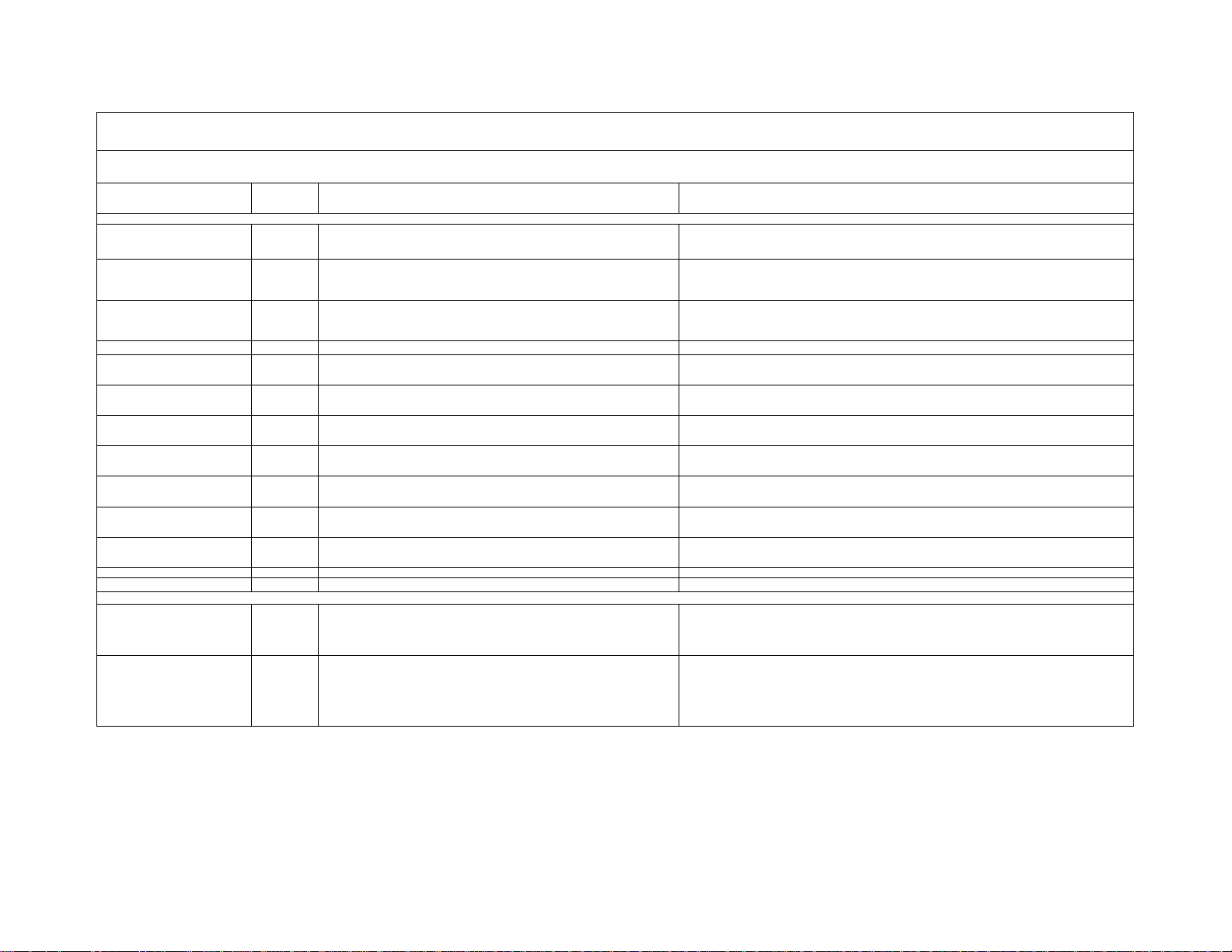
You should create a Quartus II design, enter your device I/O assignments and compile the design. Quartus II will check your pin connections with respect to I/O assignment and placement rules to ensure proper device operation. These rules are dependent on device
density, package, I/O assignments, voltage assignments and other factors that are not fully described in this document or the device handbook.
Pin Type (1st,
2nd, & 3rd
Pin Name
Supply and Reference Pins
VCCINT Power 1.2V internal logic array voltage supply pins. VCCINT also supplies power to the input buffers used for the
VCCIO[1..4,7,8] Power I/O supply voltage pins for banks 1-4, 7 & 8. Each bank can support a different voltage level. Supported
VCCPD[1..4,7,8] Power Dedicated power pins. This 3.3V supply is used to power the I/O pre-drivers and the 3.3-V/2.5-V buffers o
GND Ground Device ground pins. All GND pins should be connected to the board GND plane.
VREFB[1..4,7,8]N[2..0] Input Input reference voltage for each I/O bank. If a bank is used for a voltage-referenced I/O standard, then
VCC_PLL5_OUT Power External clock output VCCIO power for PLL5 clock outputs PLL5_OUT[1..0]p, PLL5_OUT[1..0]n,
VCC_PLL6_OUT Power External clock output VCCIO power for PLL6 clock outputs PLL6_OUT[1..0]p, PLL6_OUT[1..0]n,
VCC_PLL11_OUT Power External clock output VCCIO power for PLL11 clock outputs PLL11_OUT[1..0]p, PLL11_OUT[1..0]n,
VCC_PLL12_OUT Power External clock output VCCIO power for PLL12 clock outputs PLL12_OUT[1..0]p, PLL12_OUT[1..0]n,
VCCA_PLL[1,2,5..8,11,12] Power 1.2V Analog power for PLLs[1,2,5..8,11,12]. The designer is required to connect these pins to 1.2 V, even if the PLL is not used. Use an isolated linear supply. Power on the PLLs
VCCD_PLL[1,2,5..8,11,12] Power 1.2V Digital power for PLLs[1,2,5..8,11,12]. The designer is required to connect these pins to 1.2 V, even if the PLL is not used. Power on the PLLs operating at the same
GNDA_PLL[1,2,5..8,11,12] Ground Analog ground for PLLs[1,2,5..8,11,12]. Connect these pins to the same GND plane used by the FPGA GND pins. See Note 4.
NC No Connect No Connect Do not drive signals into these pins.
Dedicated Configuration/JTAG Pins
nIO_PULLUP Input Dedicated input that chooses whether the internal pull-ups on the user I/O pins and dual-purpose I/O pins
VCCSEL Input Dedicated input that selects which input buffer is used on configuration input pins: nCONFIG, DCLK
Function) Pin Description Connection Guidelines
LVDS, LVPECL, differential HSTL, differential SSTL, HSTL, and SSTL I/O standards.
voltages are 1.5V, 1.8V, 2.5V, and 3.3V. VCCIO[4,7,8] also supports 1.2V for 1.2V HSTL operation. For
specific I/O standards supported by Arria refer to the Arria GX Handbook .
the configuration input pins and JTAG pins. VCCPD powers the JTAG pins (TCK, TMS, TDI, and TRST)
and the following configuration pins: nCONFIG, DCLK (when used as an input), nIO_Pullup, DATA[7..0],
RUnLU, nCE, nWS, nRS, CS, nCS and CLKUSR.
these pins are used as the voltage-reference pins for that bank. All of the VREF pins within a bank are
shorted together.
PLL5_FBp/OUT2p & PLL5_FBn/OUT2n.
PLL6_FBp/OUT2p & PLL6_FBn/OUT2n.
PLL11_FBp/OUT2p & PLL11_FBn/OUT2n.
PLL12_FBp/OUT2p & PLL12_FBn/OUT2n.
(nCSO, ASDO, DATA[7..0], nWS, nRS, RDYnBSY, nCS, CS, RUnLU, PGM[], CLKUSR, INIT_DONE,
DEV_OE, DEV_CLRn) are on or off before and during configuration. A logic high (1.5 V, 1.8 V, 2.5 V, or
3.3 V) turns off the weak pull-up, while a logic low turns them on.
(when used as an input), DATA[7..0], RUnLU, nCE, nWS, nRS, CS, nCS, and CLKUSR. The 3.3-V/2.5-V
input buffer is powered by VCCPD, while the 1.8-V/1.5-V input buffer is powered by VCCIO. A logic high
(VCCPD) selects the 1.8-V/1.5-V input buffer, while a logic low selects the 3.3-V/2.5-V input buffer.
VCCSEL should be set to comply with the logic levels driven out of the configuration device or MAX II
device/microprocessor with flash memory.
All VCCINT pins require a 1.2V supply. Decoupling depends on the design decoupling requirements of the specific board. See Note
8.
Decoupling depends on the design decoupling requirements of the specific board. See Note 8.
The VCCPD pins require 3.3 V and must ramp-up from 0 V to 3.3 V within 100ms to ensure successful configuration. For Secure
Configuration this needs to power to 3.7V for no longer than one minute (on VCCPD[8] only). TDO buffer is powered by VCCIO not
VCCPD. Decoupling depends on the design decoupling requirements of the specific board. See Note 8.
If VREF pins are not used, designers should connect them to either the VCCIO in the bank in which the pin resides or GND.
Decoupling depends on the design decoupling requirements of the specific board. See Note 8.
This pin should be connected to the voltage level of the target device which PLL5 in bank 9 is driving. Refer to the data sheet for
absolute maximum voltage rating on this pin. Decoupling depends on the design decoupling requirements of the specific board. See
Note 8.
This pin should be connected to the voltage level of the target device which PLL6 in bank 10 is driving. Refer to the data sheet for
absolute maximum voltage rating on this pin. Decoupling depends on the design decoupling requirements of the specific board. See
Note 8.
This pin should be connected to the voltage level of the target device which PLL11 in bank 11 is driving. Refer to the data sheet for
absolute maximum voltage rating on this pin. Decoupling depends on the design decoupling requirements of the specific board. See
Notes 6 and 8.
This pin should be connected to the voltage level of the target device which PLL12 in bank 12 is driving. Refer to the data sheet for
absolute maximum voltage rating on this pin. Decoupling depends on the design decoupling requirements of the specific board. See
Notes 6 and 8.
operating at the same frequency should be decoupled. Decoupling depends on the design decoupling requirements of the specific
board. See Notes 4 and 8.
frequency should be decoupled. Decoupling depends on the design decoupling requirements of the specific board. See Notes 4 and
8.
The nIO-PULLUP can be tied directly to VCCPD, or use a 1 kΩ pull-up resistor or tied directly to GND depending on the use desired
for the device. Refer to the description column..
The VCCSEL input buffer is powered by VCCPD and must be hardwired to VCCPD in order to enable the 1.8V/1.5V input buffers for
configuration. VCCSEL tied to GND will enable a 3.3V/2.5V POR trip point, which may be above 1.8V. Refer to the description
column.
PCG-01002-1.1
Copyright © 2009 Altera Corp.
Page 2 of 8Pin Connection Guidelines
Page 3
Arria® GX Device Family Pin Connection Guidelines
PCG-01002-1.1
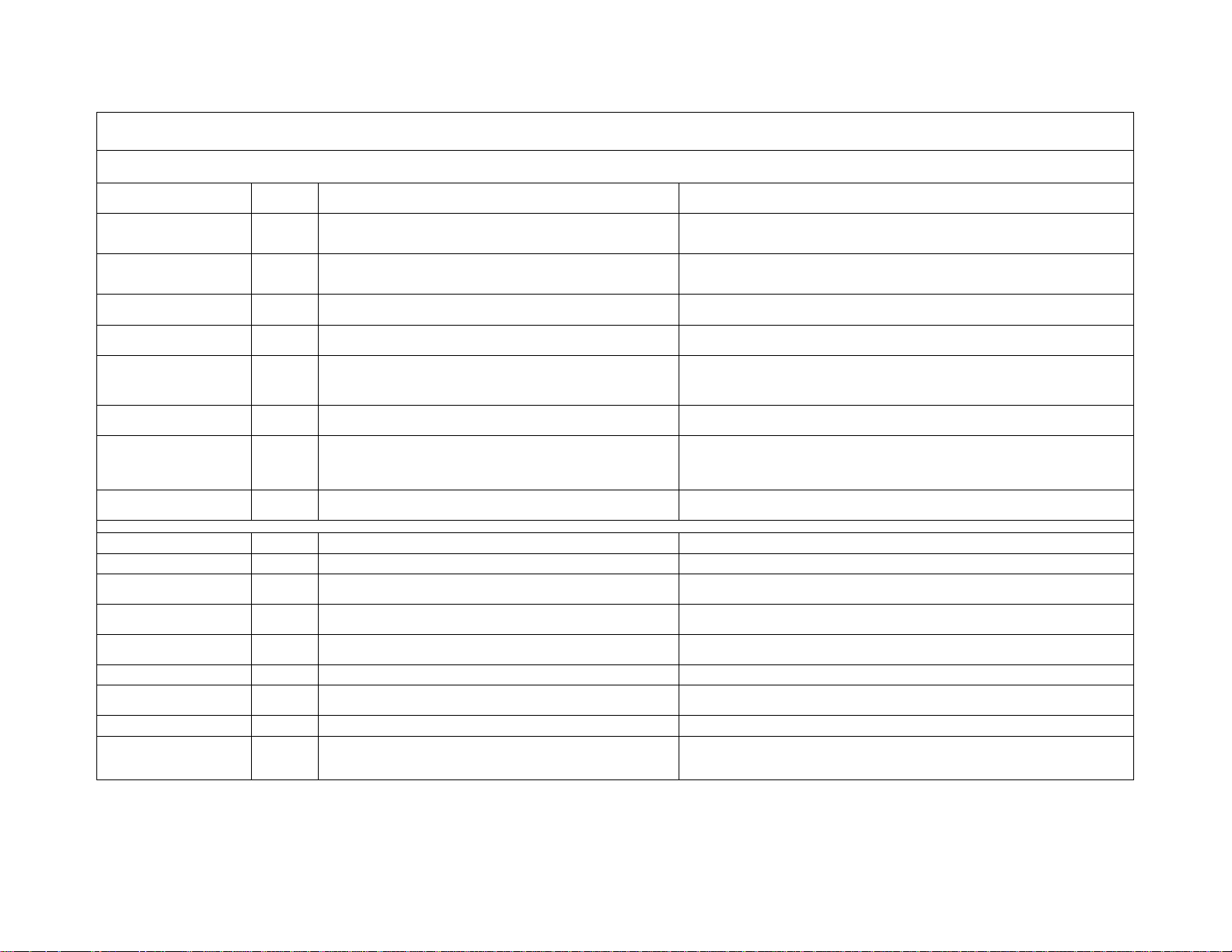
You should create a Quartus II design, enter your device I/O assignments and compile the design. Quartus II will check your pin connections with respect to I/O assignment and placement rules to ensure proper device operation. These rules are dependent on device
density, package, I/O assignments, voltage assignments and other factors that are not fully described in this document or the device handbook.
Pin Type (1st,
2nd, & 3rd
Pin Name
DCLK Input (PS, FPP)
MSEL[3..0] Input Configuration input pins that set the Arria GX device configuration scheme. These pins are internally connected through a 5kΩ resistor to GND. Do not leave these pins floating. When these pins are unused
nCE Input Dedicated active-low chip enable. When nCE is low, the device is enabled. When nCE is high, the device
nCONFIG Input Dedicated configuration control input. Pulling this pin low during user-mode will cause the FPGA to lose
CONF_DONE Bidirectional
nCEO Output Output that drives low when device configuration is complete. During multi-device configuration, this pin feeds a subsequent device’s nCE pin. During single device configuration, this pin is left
nSTATUS Bidirectional
PORSEL Input Dedicated input which selects between a POR time of 12 ms or 100 ms. A logic high (1.5-V, 1.8-V, 2.5-V,
Optional/Dual-Purpose Configuration Pins
nCSO I/O Output Output control signal from the Arria GX FPGA to the serial configuration device in AS mode that enables
ASDO I/O Output Control signal from the Arria GX FPGA to the serial configuration device in AS mode used to read out
CRC_ERROR I/O, Output Active high signal that indicates that the error detection circuit has detected errors in the configuration
DEV_CLRn I/O, Input Optional pin that allows you to override all clears on all device registers. When this pin is driven low, all
DEV_OE I/O, Input Optional pin that allows you to override all tri-states on the device. When this pin is driven low, all I/O pins
DATA0 I/O, Input Dual-purpose configuration data input pin. The DATA0 pin can be used for bit-wide configuration or as an
DATA[6..1] I/O, Input Dual-purpose configuration input data pins. The DATA[7..0] pins can be used for byte-wide configuration
DATA7 I/O, Bidirectional In the PPA configuration scheme, the DATA7 pin presents the RDYnBSY signal after the nRS signal has
INIT_DONE I/O, Output
Function) Pin Description Connection Guidelines
Output (AS)
(open-drain)
(open-drain)
(open-drain)
Dedicated configuration clock pin. In PS and FPP configuration, DCLK is used to clock configuration data
from an external source into the Arria GX device. In AS mode, DCLK is an output from the Arria GX
device that provides timing for the configuration interface.
is disabled.
its configuration data, enter a reset state and tri-state all I/O pins. Returning this pin to a logic high level
will initiate reconfiguration.
This is a dedicated configuration Done pin. As a status output, the CONF_DONE pin drives low before
and during configuration. Once all configuration data is received without error and the initialization cycle
starts, CONF_DONE is released. As a status input, CONF_DONE goes high after all data is received.
Then the device initializes and enters user mode. It is not available as a user I/O pin.
This is a dedicated configuration status pin. The FPGA drives nSTATUS low immediately after power-up
and releases it after POR time. As a status output, the nSTATUS is pulled low if an error occurs during
configuration. As a status input, the device enters an error state when nSTATUS is driven low by an
external source during configuration or initialization. It is not available as a user I/O pin.
3.3-V) selects a POR time of about 12 ms and a logic low selects POR time of about 100 ms.
the configuration device.
configuration data.
SRAM bits. This pin is optional and is used when the CRC error detection circuit is enabled.
registers are cleared; when this pin is driven high, all registers behave as programmed.
are tri-stated; when this pin is driven high, all I/O pins behave as defined in the design.
I/O pin after configuration is complete.
or as regular I/O pins. These pins can also be used as user I/O pins after configuration.
been strobed low.
This is a dual-purpose pin and can be used as an I/O pin when not enabled as INIT_DONE. When
enabled, a transition from low to high at the pin indicates when the device has entered user mode. If the
INIT_DONE output is enabled, the INIT_DONE pin cannot be used as a user I/O pin after configuration.
In PPA mode, DCLK should be tied to VCC to prevent this pin from floating.
connect them to GND. Depending on the configuration scheme used these pins should be tied to VCCPD or GND. Refer to chapter 2,
"Configuring Stratix II & Stratix II GX Devices", of the Configuration Handbook. If only JTAG configuration is used then connect these
pins to ground.
In multi-device configuration, nCE of the first device is tied directly to GND while its nCEO pin drives the nCE of the next device in the
chain. In single device configuration and JTAG programming, nCE is tied directly to GND. When using an active serial programming
header connect this pin to a 10-kΩ pull-down resistor.
If the configuration scheme uses an enhanced configuration device or EPC2, nCONFIG can be tied directly the configuration device's
nINIT_CONF pin. If this pin is not used this pin requires a connection directly or through a resistor to VCCPD.
If internal pull-up resistors on the enhanced configuration device are used, external 10-kΩ pull-up resistors should not be used on
these pins. When using EPC2 devices, only external 10-kΩ pull-up resistors should be used.
floating. For recommendations on how to connect nCEO in a chain with multiple voltages across the devices in the chain, refer to the
Configuring Arria GX Devices chapter in Volume 2 of the Arria GX Device Handbook.
The enhanced configuration devices’ and EPC2 devices’ OE and nCS pins have optional
internal programmable pull-up resistors. If internal pull-up resistors on the enhanced
configuration device are used, external 10-kΩ pull-up resistors should not be used on these pins. When using EPC2 devices, only
external 10-kΩ pull-up resistors should be used.
The PORSEL pin should be tied directly to VCCPD or GND.
When not programming the device in AS mode nCSO is not used. Also, when this pin is not used as an I/O then it is recommended to
leave the pin unconnected.
When not programming the device in AS mode ASDO is not used. Also, when this pin is not used as an I/O then it is recommended to
leave the pin unconnected.
When the dedicated output for CRC_ERROR is not used and this pin is not used as an I/O then it is recommended to leave the pin
unconnected.
When the dedicated input DEV_CLR is not used and this pin is not used as an I/O then it is recommended to tie this pin to VCCPD or
ground.
When the dedicated input DEV_OE is not used and this pin is not used as an I/O then it is recommended to tie this pin to VCCPD or
ground.
When the dedicated inputs for DATA[7..0] are not used and these pins are not used as an I/O then it is recommended to leave these
pins unconnected.
When the dedicated inputs for DATA[7..0] are not used and these pins are not used as an I/O then it is recommended to leave these
pins unconnected.
When the dedicated inputs for DATA[7..0] are not used and these pins are not used as an I/O then it is recommended to leave these
pins unconnected.
Connect this pin to a 10kΩ resistor to VCCIO3.
PCG-01002-1.1
Copyright © 2009 Altera Corp.
Page 3 of 8Pin Connection Guidelines
Page 4

Arria® GX Device Family Pin Connection Guidelines
PCG-01002-1.1
You should create a Quartus II design, enter your device I/O assignments and compile the design. Quartus II will check your pin connections with respect to I/O assignment and placement rules to ensure proper device operation. These rules are dependent on device
density, package, I/O assignments, voltage assignments and other factors that are not fully described in this document or the device handbook.
Pin Type (1st,
2nd, & 3rd
Pin Name
nCS, CS I/O, Input These are chip-select inputs that enable the Arria GX device in the passive parallel asynchronous
nRS I/O, Input Read strobe input pin. A low input directs the device to drive the RDYnBSY signal on the DATA7 pin. In
nWS
CLKUSR I/O, Input Optional user-supplied clock input. Synchronizes the initialization of one or more devices. If this pin is not
RDYnBSY I/O, Output Ready not busy output. A high output indicates that the target device is ready to accept another data byte.
PGM[2..0] I/O, Output These output pins control one of eight pages in the memory (either flash or enhanced configuration
RUnLU I/O, Input Input that selects between remote update and local update. A logic high (1.5 V, 1.8 V, 2.5 V, 3.3 V)
TCK Input Dedicated JTAG test clock input pin. Connect this pin to a 1kΩ resistor to GND. The JTAG circuitry can be disabled by connecting TCK to GND.
TMS Input Dedicated JTAG test mode input pin. Connect this pin to a 10kΩ resistor to VCCPD. The JTAG circuitry can be disabled by connecting TMS to VCC.
TDI Input Dedicated JTAG test data input pin. Connect this pin to a 10kΩ resistor to VCCPD. The JTAG circuitry can be disabled by connecting TDI to VCC.
TDO Output Dedicated JTAG test data output pin. The JTAG circuitry can be disabled by leaving TDO unconnected.
TRST Input Dedicated active low JTAG test reset input pin. TRST is used to asynchronously reset the JTAG boundary
Clock and PLL Pins
CLK[1,3]p Clock, Input Dedicated clock input pins 1 and 3 that can also be used for data inputs. These pins do not support OCT
CLK[1,3]n Clock, Input Dedicated negative clock input pins for differential clock input that can also be used for data inputs. These
CLK[2,0]p/DIFFIO_RX_C[1,0]p I/O, Clock These pins can be used as I/O pins, clock input pins, or the positive terminal data pins of differential
CLK[2,0]n/DIFFIO_RX_C[1,0]n I/O, Clock These pins can be used as I/O pins, the negative clock input pins for differential clock input, or the
CLK[4-7,12-15]p I/O, Clock These pins can be used as I/O pins or clock input pins. When not used these pins can be tied to GND or left unconnected. If unconnected, use Quartus II software programmable options to
CLK[4-7,12-15]n I/O, Clock These pins can be used as I/O pins or negative clock input pins for differential clock inputs. When not used these pins can be tied to GND or left unconnected. If unconnected, use Quartus II software programmable options to
PLL_ENA Input Dedicated input pin that drives the optional pllena port of all or a set of PLLs. If a PLL uses the pllena port, drive the PLL_ENA pin low to reset all PLLs including
FPLL[8..7]CLKp Clock, Input Dedicated positive clock inputs for fast PLLs (PLLs 7 and 8) which can also be used for data inputs.
Function) Pin Description Connection Guidelines
configuration mode. Drive nCS low and CS high to target a device for configuration. If a design requires
an active high enable, use the CS pin and drive the nCS pin low. If a design requires an active low enable,
use the nCS pin and drive the CS pin high. Configuration will be paused when either signal is inactive.
Hold the nCS and CS pins active during configuration and initialization. The design can use these pins as
user I/O pins after configuration.
non-PPA schemes, it functions as a user I/O during configuration, which means it is tri-stated. This pin ca
be used as a user I/O pin after configuration.
I/O, Input
Active-low write strobe input to latch a byte of data on the DATA pins. This pin can be used as a user I/O
pin after configuration.
enabled for use as a user-supplied configuration clock, it can be used as a user I/O pin.
A low output indicates that the target device is not ready to receive another data byte. This pin can be
used as a user I/O pin after configuration.
device) when using a remote system update mode. When not using remote update or local update
configuration modes, these pins are user I/O pins.
selects remote update and a logic low selects local update. When not using remote update or local
update configuration modes, this pin is available as general-purpose user I/O pin.
scan circuit.
Rd and cannot be used as output pins. The programmable weak pull up resistor is not supported on
these pins.
pins do not support OCT Rd and cannot be used as output pins. The programmable weak pull up resistor
is not supported on these pins.
receiver channels.
negative data pins of differential receiver channels.
These pins do not support OCT Rd and cannot be used as output pins. The programmable weak pull up
resistor is not supported on these pins.
When the dedicated inputs for nCS, CS are not used and these pins are not used as an I/O then it is recommended to leave these
pins unconnected.
If the nRS pin is not used in PPA mode, it should be tied to VCCIO8.
n
If the device is not being programmed in PPA mode and the pin is not being used then it is recommended to connect the nWS pin to
the power bank this pin resides in.
If the CLKUSR pin is not used as a configuration clock input and the pin is not used as an I/O then it is recommended to connect this
pin to ground.
If the device is not being programmed in PPA mode and the pin is not being used as an I/O then it is recommended to leave the
RDYnBSY pin unconnected.
If the PGM[2..0] pins are not used as page select output and these pins are not used as I/O then it is recommended to leave these
pins unconnected.
If the RUnLU pin is not used as a local/remote configuration input and the pin is not used as an I/O then it is recommended to leave
this pin unconnected.
The JTAG circuitry can be disabled by connecting TRST to GND. If JTAG is not disabled then connect this pin to VCCPD.
Connect unused pins to the VCCIO of the bank where the pin resides.
Connect unused pins to GND.
When not used these pins can be tied to GND or left unconnected. If unconnected, use Quartus II software programmable options to
internally bias these pins. They can be reserved as inputs tristate with weak pull up resistor enabled, or as outputs driving GND. See
Note 5.
When not used these pins can be tied to GND or left unconnected. If unconnected, use Quartus II software programmable options to
internally bias these pins. They can be reserved as inputs tristate with weak pull up resistor enabled, or as outputs driving GND. See
Note 5.
internally bias these pins. They can be reserved as inputs tristate with weak pull up resistor enabled, or as outputs driving GND.
internally bias these pins. They can be reserved as inputs tristate with weak pull up resistor enabled, or as outputs driving GND.
the counters to their default state. If VCCSEL = 0, then you must drive the PLL_ENA
with a 3.3/2.5 V signal to enable the PLLs. If VCCSEL = 1, connect PLL_ENA to 1.8/1.5 V to enable the PLLs.
Connect unused pins to the VCCIO of the bank where the pin resides. See Note 6.
PCG-01002-1.1
Copyright © 2009 Altera Corp.
Page 4 of 8Pin Connection Guidelines
Page 5

Arria® GX Device Family Pin Connection Guidelines
PCG-01002-1.1
You should create a Quartus II design, enter your device I/O assignments and compile the design. Quartus II will check your pin connections with respect to I/O assignment and placement rules to ensure proper device operation. These rules are dependent on device
density, package, I/O assignments, voltage assignments and other factors that are not fully described in this document or the device handbook.
Pin Type (1st,
2nd, & 3rd
Pin Name
FPLL[8..7]CLKn Clock, Input Dedicated negative clock inputs associated with the FPLL[7,8]CLKp pins which can also be used for data
PLL5_OUT[1,0]p Output Optional positive external clock outputs [1,0] from enhanced PLL 5. These pins can be differential (two
PLL5_OUT[1,0]n Output Optional negative external clock outputs [1,0] from enhanced PLL5. If the clock outputs are single ended,
PLL6_OUT[1,0]p Output Optional positive external clock outputs [1,0] from enhanced PLL 6. These pins can be differential (two
PLL6_OUT[1,0]n Output Optional negative external clock outputs [1,0] from enhanced PLL6. If the clock outputs are single ended,
PLL11_OUT[1,0]p Output Optional positive external clock outputs [1,0] from enhanced PLL 11. These pins can be differential (two
PLL11_OUT[1,0]n Output Optional negative external clock outputs [1,0] from enhanced PLL11. If the clock outputs are single
PLL12_OUT[1,0]p Output Optional positive external clock outputs [1,0] from enhanced PLL 12. These pins can be differential (two
PLL12_OUT[1,0]n Output Optional negative external clock outputs [1,0] from enhanced PLL12. If the clock outputs are single
PLL[6..5]_FBp/OUT2p I/O, Input, Output These pins can be used as I/O pins, positive external feedback input pins or external clock outputs for
PLL[6..5]_FBn/OUT2n I/O, Input, Output These pins can be used as I/O pins, negative external feedback input PLL[6,5]_FBp or negative terminal
PLL[12..11]_FBp/OUT2p I/O, Input, Output These pins can be used as I/O pins, positive external feedback input pins or positive external clock output
PLL[12..11]_FBn/OUT2n
Dual-Purpose Differential & External Memory Interface Pins
DIFFIO_RX[50..1]p I/O, Input Dual-purpose differential receiver channels. These channels can be used for receiving LVDS compatible
DIFFIO_RX[50..1]n I/O, Input Dual-purpose differential receiver channels. These channels can be used for receiving LVDS compatible
DIFFIO_TX[51..0]p I/O, Output Dual-purpose differential transmitter channels. These channels can be used for transmitting LVDS
DIFFIO_TX[51..0]n I/O, Output Dual-purpose differential transmitter channels. These channels can be used for transmitting LVDS
DQS[17..0][T,B] I/O, DQS Optional data strobe signal for use in external memory interfacing. These pins drive to dedicated DQS
DQ[17..0][T,B] (x4) I/O, DQ Optional data signal for use in external memory interfacing. The order of the DQ bits within a designated
Function) Pin Description Connection Guidelines
inputs. These pins do not support OCT Rd and cannot be used as output pins. The programmable weak
pull up resistor is not supported on these pins.
output pin pairs) or single ended (four clock outputs from PLL5).
then each pair of pins (i.e., PLL5_OUT0p and PLL5_OUT0n are considered one pair) can be either in
phase or 180 degrees out of phase.
output pin pairs) or single ended (four clock outputs from PLL6).
then each pair of pins (i.e., PLL6_OUT0p and PLL6_OUT0n are considered one pair) can be either in
phase or 180 degrees out of phase.
output pin pairs) or single ended (four clock outputs from PLL11).
ended, then each pair of pins (i.e., PLL11_OUT0p and PLL11_OUT0n are considered one pair) can be
either in phase or 180 degrees out of phase.
output pin pairs) or single ended (four clock outputs from PLL12).
ended, then each pair of pins (i.e., PLL12_OUT0p and PLL12_OUT0n are considered one pair) can be
either in phase or 180 degrees out of phase.
PLL[6,5].
clock output pins for differential clock output.
for PLL[12..11].
I/O, Input, Output These pins can be used as I/O pins, negative external feedback input PLL[12..11]_FBp or negative
external clock output pins for differential clock output.
signals. Pins with a "p" suffix carry the positive signal for the differential channel. If not used for differential
signaling, these pins are available as user I/O pins.
signals. Pins with an "n" suffix carry the negative signal for the differential channel. If not used for
differential signaling, these pins are available as user I/O pins.
compatible signals. Pins with a "p" suffix carry the positive signal for the differential channel. If not used fo
differential signaling, these pins are available as user I/O pins.
compatible signals. Pins with an "n" suffix carry the negative signal for the differential channel. If not used
for differential signaling, these pins are available as user I/O pins.
phase shift circuitry. The shifted DQS signal can also drive to internal logic.
DQ bus is not important; however, use caution when making pin assignments if you plan on migrating to a
different memory interface that has a different DQ bus width. Analyze the available DQ pins across all
pertinent DQS columns in the pin list.
Connect unused pins to GND. See Note 6.
When these pins are not used they may be left floating.
When these pins are not used they may be left floating.
When these pins are not used they may be left floating.
When these pins are not used they may be left floating.
When these pins are not used they may be left floating. See Notes 4 and 6.
When these pins are not used they may be left floating. See Notes 4 and 6.
When these pins are not used they may be left floating. See Notes 4 and 6.
When these pins are not used they may be left floating. See Notes 4 and 6.
When not used these pins can be tied to GND or left unconnected. If unconnected, use Quartus II software programmable options to
internally bias these pins. They can be reserved as inputs tristate with weak pull up resistor enabled, or as outputs driving GND.
When not used these pins can be tied to GND or left unconnected. If unconnected, use Quartus II software programmable options to
internally bias these pins. They can be reserved as inputs tristate with weak pull up resistor enabled, or as outputs driving GND.
s
When not used these pins can be tied to GND or left unconnected. If unconnected, use Quartus II software programmable options t
internally bias these pins. They can be reserved as inputs tristate with weak pull up resistor enabled, or as outputs driving GND. See
Notes 4 and 6.
When not used these pins can be tied to GND or left unconnected. If unconnected, use Quartus II software programmable options to
internally bias these pins. They can be reserved as inputs tristate with weak pull up resistor enabled, or as outputs driving GND. See
Notes 4 and 6.
When these IO pins are not used they can be tied to the VCCIO of the bank that they reside in, GND or left unconnected. See Note 5.
When these IO pins are not used they can be tied to the VCCIO of the bank that they reside in, GND or left unconnected. See Note 5.
When these IO pins are not used they can be tied to the VCCIO of the bank that they reside in, GND or left unconnected. See No
r
When these IO pins are not used they can be tied to the VCCIO of the bank that they reside in, GND or left unconnected. See No
When these IO pins are not used they can be tied to the VCCIO of the bank that they reside in, GND or left unconnected. See Note 7.
When these IO pins are not used they can be tied to the VCCIO of the bank that they reside in, GND or left unconnected. See Note 7.
o
te 5.
te 5.
PCG-01002-1.1
Copyright © 2009 Altera Corp.
Page 5 of 8Pin Connection Guidelines
Page 6

Arria® GX Device Family Pin Connection Guidelines
PCG-01002-1.1
You should create a Quartus II design, enter your device I/O assignments and compile the design. Quartus II will check your pin connections with respect to I/O assignment and placement rules to ensure proper device operation. These rules are dependent on device
density, package, I/O assignments, voltage assignments and other factors that are not fully described in this document or the device handbook.
Pin Type (1st,
2nd, & 3rd
Pin Name
Transceiver (I/O Banks) Pins
VCCP Power GX bank [15..13] PCS power. This power is connected to 1.2V. Connect VCCP to an isolated 1.2V linear regulator. These pins need to be isolated from noisy digital voltage planes. Decoupling
Function) Pin Description Connection Guidelines
depends on the design decoupling requirements of the specific board design. See Note 8.
VCCR Power GX bank [15..13] receiver analog power. This power is connected to 1.2V. Connect VCCR to a 1.2V linear regulator. These pins may be tied to the same 1.2V plane as VCCT_B[] and/or VCCL_B[]. However,
VCCT_B[15..13] Power GX bank [15..13] transmitter analog power. This power is connected to 1.2V. Connect VCCT_B[] to a 1.2V linear regulator. These pins may be tied to the same 1.2V plane as VCCR and/or VCCL_B[]. However,
VCCA Power GX bank [15..13] analog power. This power is connected to 3.3V. Connect VCCA to a 3.3V linear regulator. Decoupling depends on the design decoupling requirements of the specific board design.
VCCH_B[15..13] Power GX bank [15..13] Transmitter driver analog power. This power is connected to 1.2V or 1.5V. Connect VCCH_B[] to a 1.2V or 1.5V linear regulator. Decoupling depends on the design decoupling requirements of the specific
VCCL_B[15..13] Power GX bank [15..13] VCO analog power and general transceiver clock circuitry. This power is connected to
GXB_RX[11..0]p Input High speed positive differential receiver channels. These pins should be ac coupled when used. Connect all unused GXB_RXp pins to the VCCR 1.2V plane either individually through
GXB_RX[11..0]n Input High speed negative differential receiver channels. These pins should be ac coupled when used. Connect all unused GXB_RXn pins either individually to GND through a 10kΩ resistor
GXB_TX[11..0]p Output High speed positive differential transmitter channel. These pins should be ac coupled when used. Connect all unused GXB_TXp pins to the VCCT_B[] or VCCR (if tied together w/
GXB_TX[11..0]n Output High speed negative differential transmitter channels. These pins should be ac coupled when used. Connect all unused GXB_TXn pins either individually to GND through a 10kΩ resistor or
REFCLK[0,1]_B[15..13]p Input High speed differential I/O reference clock positive. These pins should be ac coupled when used. Connect all unused REFCLK[0,1]_B[]p pins to the VCCT_B[] or VCCR (if tied together
REFCLK[0,1]_B[15..13]n Input High speed differential I/O reference clock negative. These pins should be ac coupled when used. Connect all unused REFCLK[0,1]_B[]n pins either individually to GND through a 10kΩ
RREFB[15..13] Input Reference resistor for GX side banks. These pins should be connected to a 2.00kΩ 1% resistor to GND. In the PCB layout, the trace from this pin to the resistor needs to be
1.2V.
for the best jitter performance at high data rates this plane should be isolated from all other power supplies. Decoupling depends on
the design decoupling requirements of the specific board design. See Note 8.
for the best jitter performance at high data rates this plane should be isolated from all other power supplies. Decoupling depends on
the design decoupling requirements of the specific board design. See Notes 3 and 8.
See Note 8.
board design. See Notes 3 and 8.
Connect VCCL_B[] to a 1.2V linear regulator. These pins may be tied to the same 1.2V plane as VCCT_B[] and/or VCCR. However,
for the best jitter performance at high data rates this plane should be isolated from all other power supplies. Decoupling depends on
the design decoupling requirements of the specific board design. See Notes 3 and 8.
a 10kΩ resistor or tie all unused pins together through a single 10kΩ resistor. Insure that the trace from the pins to the resistor(s) are
as short as possible. See Note 2.
or tie all unused pins together through a single 10kΩ resistor. Insure that the trace from the pins to the resistor(s) are as short as
possible. See Note 2.
VCCT_B[]) 1.2V plane either individually through a 10kΩ resistor or tie all unused pins together through a single 10kΩ resistor. Insure
that the trace from the pins to the resistor(s) are as short as possible. See Note 2.
tie all unused pins together through a single 10kΩ resistor. Insure that the trace from the pins to the resistor(s) are as short as
possible. See Note 2.
w/ VCCT_B[]) 1.2V plane either individually through a 10kΩ resistor or tie all unused pins together through a single 10kΩ resistor.
Insure that the trace from the pins to the resistor(s) are as short as possible. See Note 3.
resistor or tie all unused pins together through a single 10kΩ resistor. Insure that the trace from the pins to the resistor(s) are as short
as possible. See Note 3.
routed so that it avoids any aggressor signals. See Note 3.
Altera provides these guidelines only as recommendations. It is the responsibility of the designer to apply simulation results to the design to verify proper device functionality.
Notes:
1) This pin connection guideline is created based on the largest Arria GX device (EP1AGX90E)
2) Transceiver signals GXB_RX[11..0] and GXB_TX[11..0] are device specific.
EP1AGX20CF780 contains 4 transceivers GXB_RX[3..0], and GXB_TX[3..0].
EP1AGX20CF484, EP1AGX35C, EP1AGX50C and EP1AGX60C contains 4 transceivers GXB_RX[7..4], and GXB_TX[7..4].
EP1AGX35D, EP1AGX50D and EP1AGX60D contain 8 transceivers GXB_RX[7..0], and GXB_TX[7..0].
EP1AGX60E, and EP1AGX90E contain 12 transceivers GXB_RX[11..0], and GXB_TX[11..0].
PCG-01002-1.1
Copyright © 2009 Altera Corp.
Page 6 of 8Pin Connection Guidelines
Page 7

Arria® GX Device Family Pin Connection Guidelines
PCG-01002-1.1
You should create a Quartus II design, enter your device I/O assignments and compile the design. Quartus II will check your pin connections with respect to I/O assignment and placement rules to ensure proper device operation. These rules are dependent on device
density, package, I/O assignments, voltage assignments and other factors that are not fully described in this document or the device handbook.
Pin Type (1st,
2nd, & 3rd
Pin Name
3) Pins VCCT_B[15..13], VCCH_B[15..13], REFCLK[0,1]_B[15..13], RREFB[15..13], and VCCL_B[15..13] refer to the bank number of the transceiver.
EP1AGX20CF780 consists of 4 transceivers in Bank 13.
EP1AGX20CF484, EP1AGX35C, EP1AGX50C and EP1AGX60C consists of 4 transceivers in Bank 14.
EP1AGX35D, EP1AGX50D and EP1AGX60D consists of 8 transceivers in Banks 13 and 14.
EP1AGX60E, and EP1AGX90E consists of 12 transceivers in Banks 13 - 15.
4) EP1AGX20C, EP1AGX35C/D, EP1AGX50C, EP1AGX50DF780 and EP1AGX60C/D only have PLL(1, 2, 5 & 6), EP1AGX50DF1152, EP1AGX60E and EP1AGX90E have PLL(1,2, 5, 6, 7, 8, 11 & 12).
5) The differential TX/RX count for each device and package is different.
EP1AGX20C, EP1AGX35C/D, EP1AGX50C, EP1AGX50DF780 and EP1AGX60C/D consists of 29 transmit and 29 receive differential IO, and 2 clock/receive differential IO pins, (CLK[2,0]/DIFFIO_RX_C[1,0]).
EP1AGX50DF1152, EP1AGX60E consists of 42 transmit and 40 receive differential IO, and 2 clock/receive differential IO pins, (CLK[2,0]/DIFFIO_RX_C[1,0]).
EP1AGX90E consists of 45 transmit and 45 receive differential IO, and 2 clock/receive differential IO pins, (CLK[2,0]/DIFFIO_RX_C[1,0]).
6) EP1AGX20C and EP1AGX35C/D do not have the following signals: FPLL[8..7]CLK, PLL11_OUT[1,0], PLL12_OUT[1,0], PLL[12..11]_FBp/OUT2, VCC_PLL11_OUT, and VCC_PLL12_OUT.
EP1AGX50C, and EP1AGX60C do not have the following signals: FPLL[8..7]CLK, PLL11_OUT[1,0], PLL12_OUT[1]p/n, PLL12_OUT[0]n, PLL[11]_FBp/OUT2p/n, PLL[12]_FBp/OUT2p, VCC_PLL11_OUT, and VCC_PLL12_OUT.
EP1AGX50DF780 and EP1AGX60DF780 do not have the following signals: FPLL[8..7]CLK, PLL11_OUT[1]p/n, PLL11_OUT[0]p, PLL12_OUT[1]p/n, PLL12_OUT[0]n, PLL[11]_FBp/OUT2p/n, PLL[12]_FBp/OUT2p, VCC_PLL11_OUT, and VCC_PLL12_OUT.
EP1AGX50DF1152, EP1AGX60EF1152 and EP1AGX90EF1152 only have 8 PLLs. Although the following pin names use PLL labels, they are IO pins only and should not be construed as PLL pins. For these devices ONLY the power source is as indicated below.
a. PLL11_OUTn (C17 in the EP1AGX50DF780 and EP1AGX60DF780) - uses bank 3 power supply, VCCIO3
b. PLL12_FBn/OUT2n (AE16 in the EP1AGX50DF780 and EP1AGX60DF780) and (AB9 in EP1AGX50C and EP1AGX60C) - uses bank 8 power supply, VCCIO8
c. PLL12_OUT0p (AF16 in the EP1AGX50DF780 and EP1AGX60DF780) and (W11 in EP1AGX50C and EP1AGX60C) - uses bank 8 power supply, VCCIO8
7) EP1AGX20CF484 and EP1AGX35CF484 support either (2 x4), or (1, x8) DQ and DQS bus modes.
EP1AGX50CF484 and EP1AGX60CF484 support (2 x4) DQ and DQS bus modes.
EP1AGX20CF780 and EP1AGX35D, EP1AGX50DF780 and EP1AGX60DF780 support either (18 x4), (8, x8/x9), or (4, x16/x18) DQ and DQS bus modes.
EP1AGX50DF1152, EP1AGX60EF1152 and EP1AGX90EF1152 support either (36 x4), (18, x8/x9), (8, x16/x18) or (4, x32/x36) DQ and DQS bus modes.
8) Capacitance values for the power supply should be selected after consideration of the amount of power they need to supply over the frequency of operation of the particular circuit being decoupled. A target impedance for the power plane should be calculated based
on current draw and voltage droop requirements of the device/supply. The power plane should then be decoupled using the appropriate number of capacitors. On-board capacitors do not decouple higher than 100 MHz due to “Equivalent Series Inductance” of the
mounting of the packages. Proper board design techniques such as interplane capacitance with low inductance should be considered for higher frequency decoupling. To assist in decoupling analysis Altera's Power Distribution Network (PDN) design tool serves as an
excellent decoupling analysis tool.
Power Distribution Network Design Tool
9) Altera highly recommends using an independent PCB via for each independent power or ground ball on the package. Sharing power or ground pin vias on the PCB could lead to noise coupling into the device and result in reduced jitter performance.
Function) Pin Description Connection Guidelines
PCG-01002-1.1
Copyright © 2009 Altera Corp.
Page 7 of 8Pin Connection Guidelines
 Loading...