

Page 1
Page 2

CONTENTS
CHAPTER 1 INTRODUCTION OF THE PCA CARD...............................................................................2
1.1 Features ......................................................................................................................................................2
1.2 About the KIT.............................................................................................................................................3
1.3 Getting Help ...............................................................................................................................................4
CHAPTER 2 PCA CARD ARCHITECTURE............................................................................................. 5
2.1 Layout and Components.............................................................................................................................5
2.2 Block Diagram of the PCA Board..............................................................................................................6
CHAPTER 3 BOARD COMPONENT.......................................................................................................8
3.1 PCIe Edge Connector.................................................................................................................................8
3.2 PCIe Cable Connector..............................................................................................................................10
3.3 Switches....................................................................................................................................................13
3.4 LEDs.........................................................................................................................................................16
CHAPTER 4 SET UP ON PCA...............................................................................................................18
4.1 Introduction..............................................................................................................................................18
4.2 System Requirements...............................................................................................................................18
CHAPTER 5 APPENDIX......................................................................................................................25
5.1 Revision History.......................................................................................................................................25
5.2 Copyright Statement.................................................................................................................................25
1
Page 3
Chapter 1
Introduction of the PCA Card
PCA(PCIe Cable Adapter),which is used to connect PCIe upstream slot with downstream target
board by a PCIe X4 cable , supports the PCIe X4 & X1 mode. PCA card can provide programmable
equalization, amplification, and de-emphasis for PCIe transceiver signal by using 8 select bits. It is
also available to optimize performance over a variety of physical mediums by reducing
Inter-symbol interference.
2
1.1
1.1
Features
Features
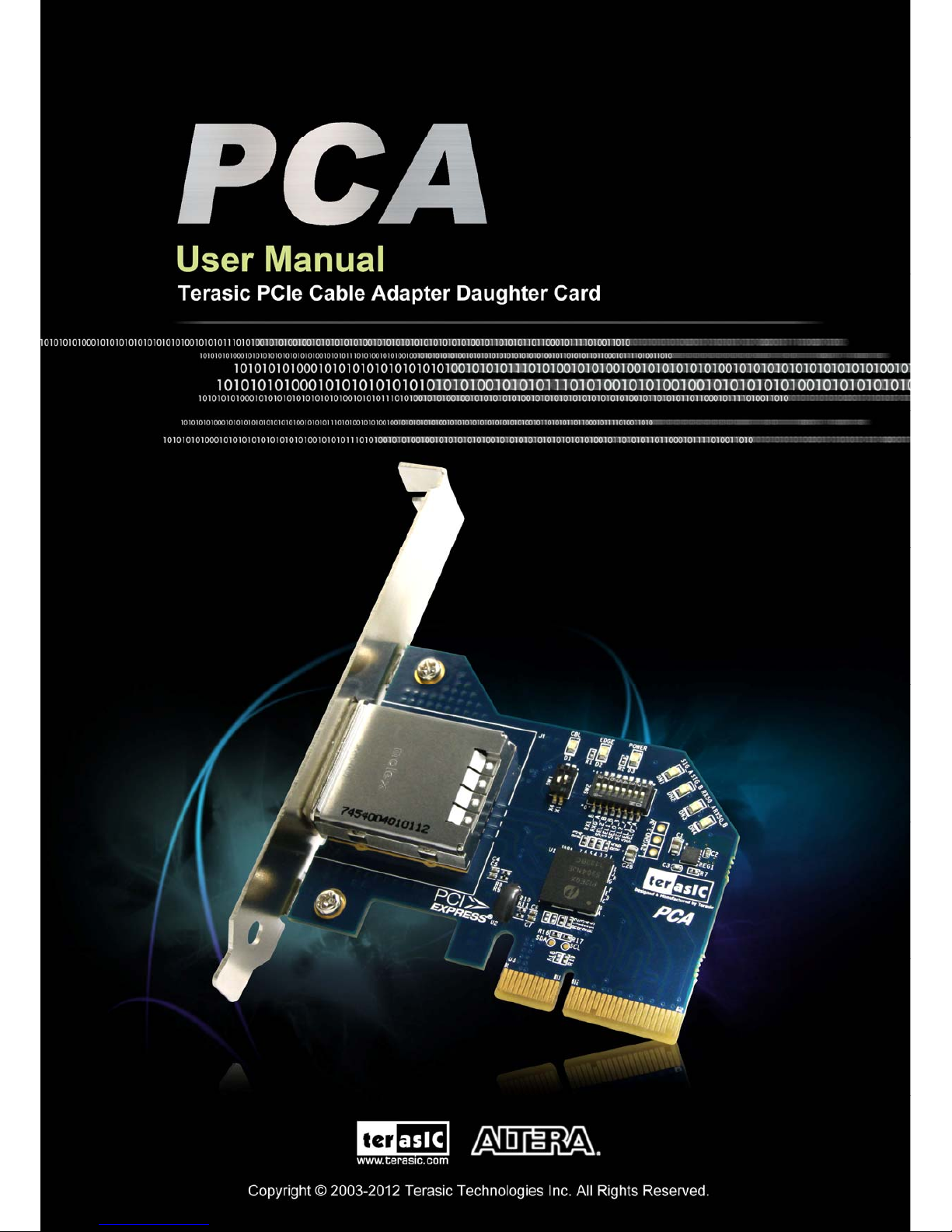
Figure 1-1 shows a photograph of the PCA Card.
Figure 1-1 Layout of the PCA card
Page 4
The key features of the card are listed below:
• Up to 5.0Gbps PCIe 2.0 Serial Re-Driver
• PCIe X4 Gen 2
• Adjustable receiver equalization
• Adjustable transmitter amplitude and de-emphasis
3
1.2
1.2
About the KIT
About the KIT
The PCA kit will come with the following contents:
• PCA card
Please visit PCIe_Cable.terasic.com download the PCA user manual.
Figure 1-2 shows the photograph of the PCA kit content.
Figure 1-2 PCA kit package contents
Page 5

4
1.3
1.3
Getting Help
Getting Help
Here is information of how to get help if you encounter any problem:
Terasic Technologies
• Tel: +886-3-550-8800
• Email: support@terasic.com
Page 6
Chapter 2
PCA Card Architecture
This chapter provides information about architecture and block diagram of the PCA board.
5
2.1
2.1
Layout and Components
Layout and Components
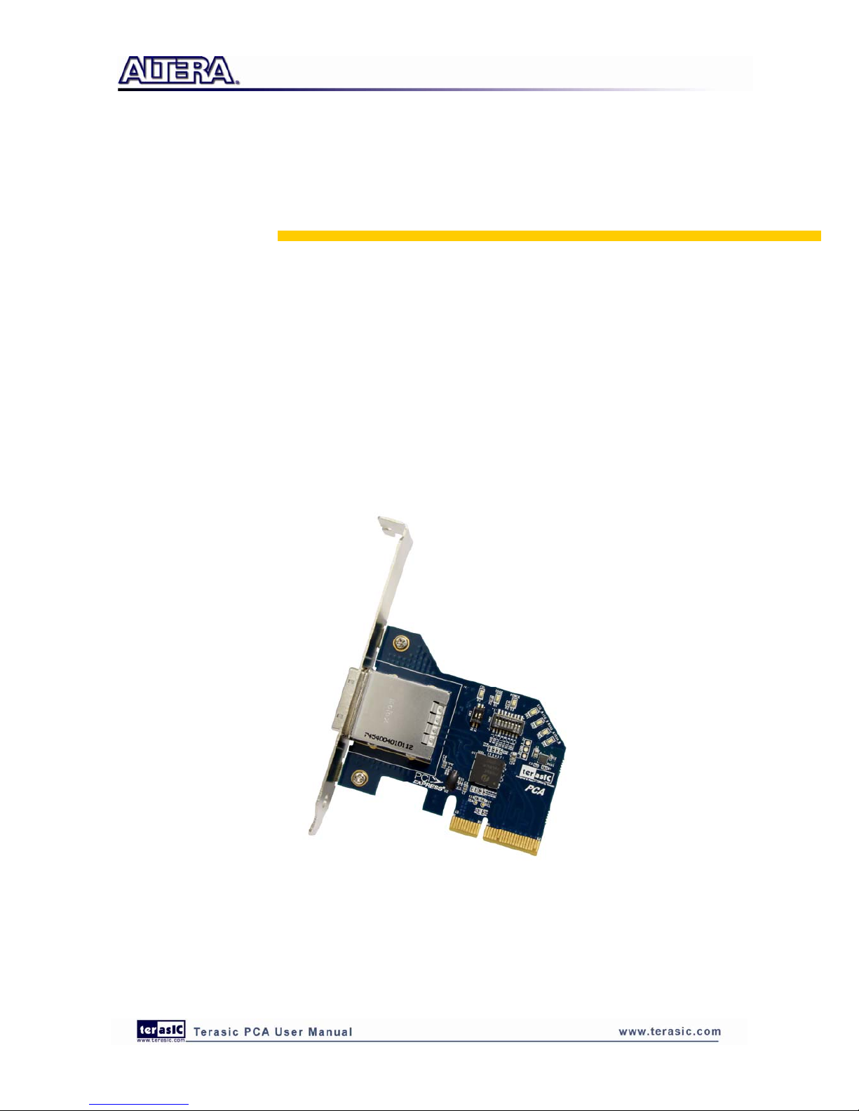
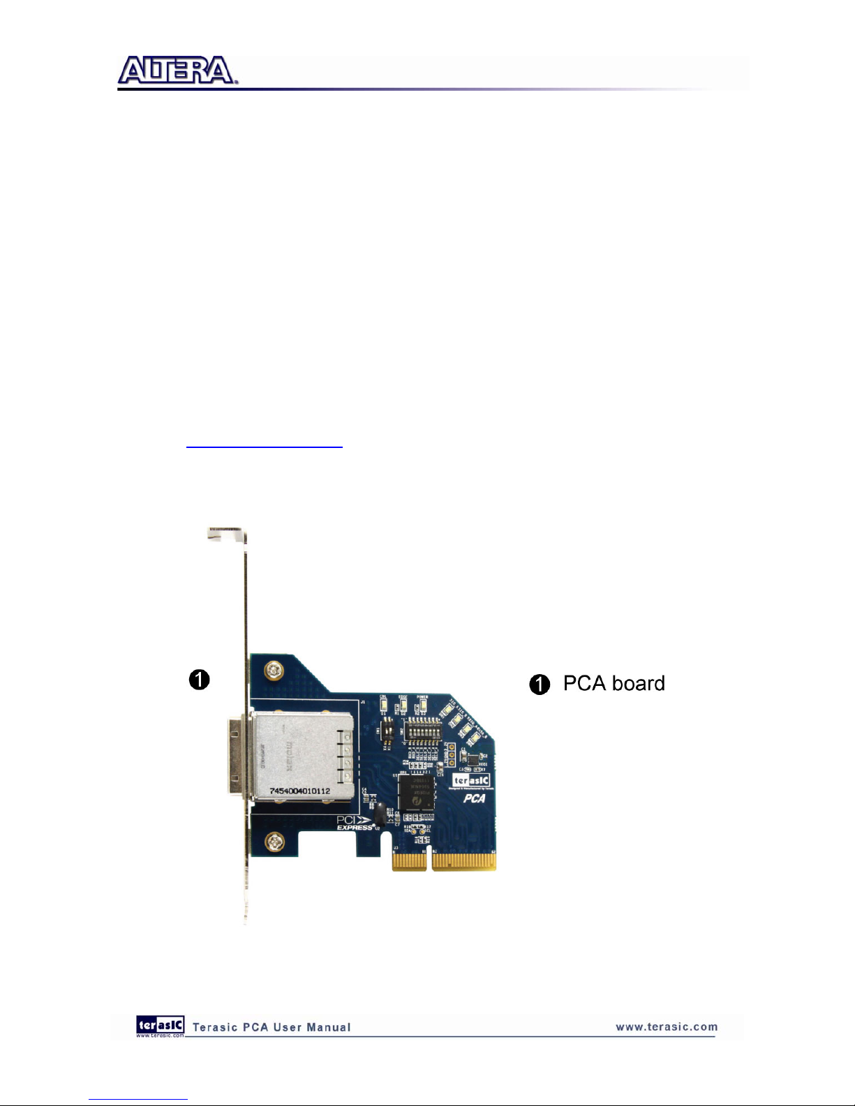
The picture of the PCA card is shown in Figure 2-1 and Figure 2-2. It depicts the layout of the
board and indicates the locations of the connectors and key components.
Figure 2-1 The PCA Card PCB and component diagram (top view)
Page 7
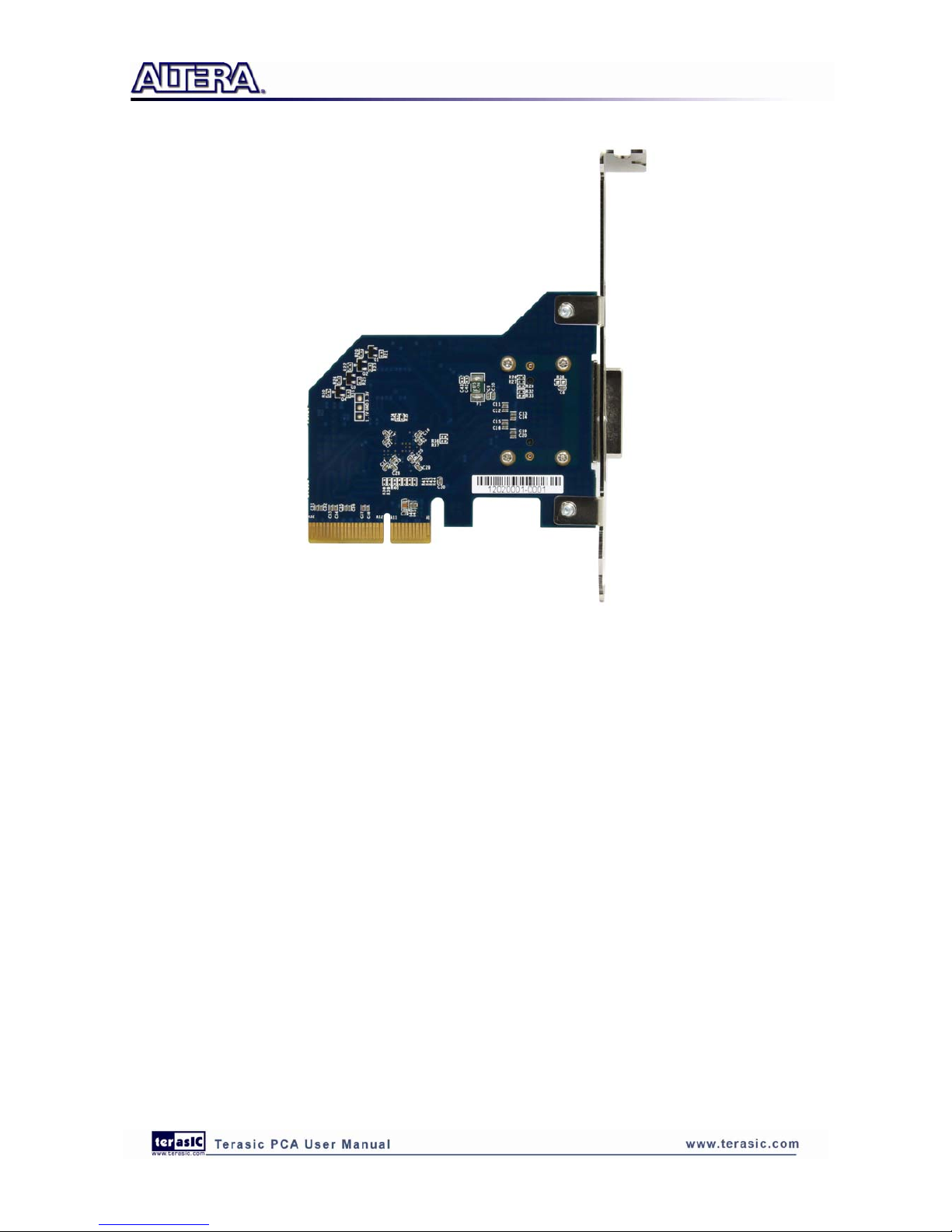
Figure 2-2 The PCA Card PCB and component diagram (bottom v i ew)
6
2.2
2.2
Block Diagram of the PCA Board
Block Diagram of the PCA Board
Figure 2-3 shows the block diagram of the PCA card.
Page 8
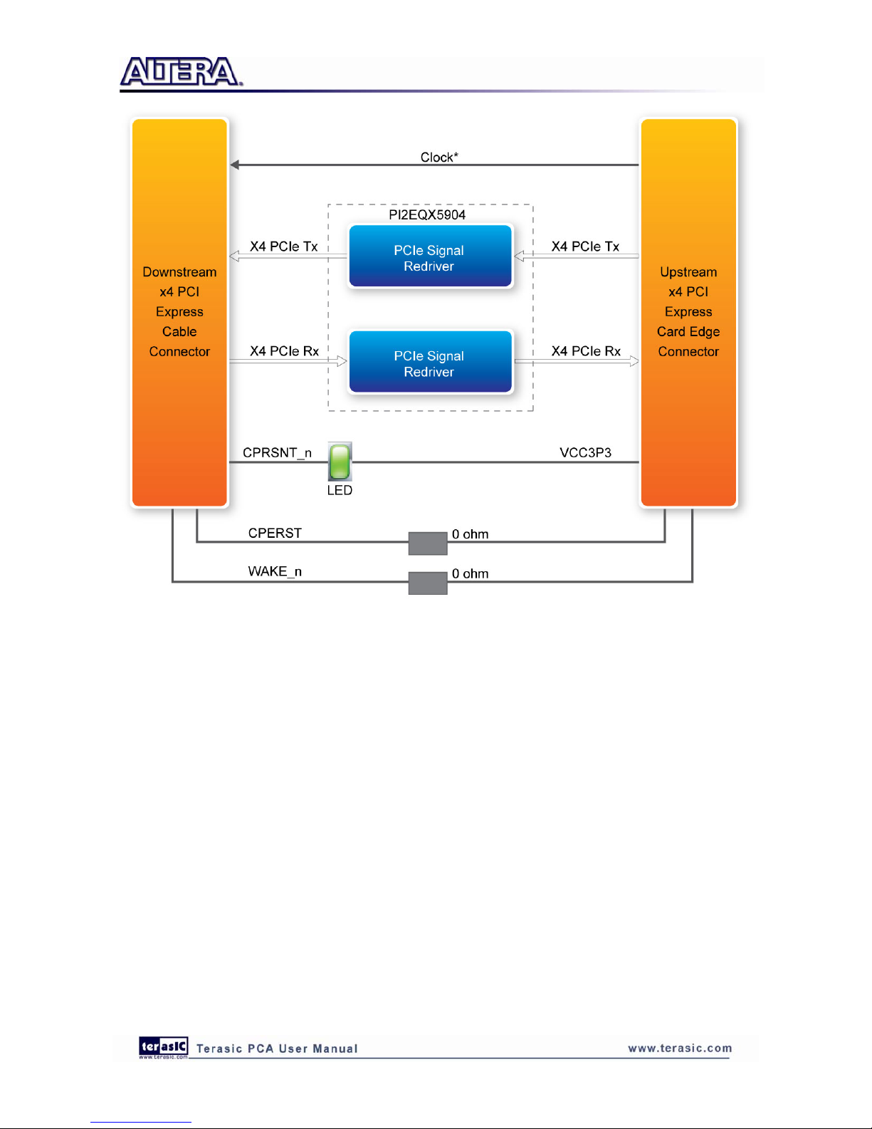
Figure 2-3 Block Diagram of PCA card
7
Page 9

Chapter 3
Board Component
This chapter describes the specifications of the on board components.
8
3.1
3.1
PCIe Edge Connector
PCIe Edge Connector
This Edge connector is used to connect the PCA with PC motherboard PCIe slot, as show Figure
3-1 and Figure 3-2.
Figure 3-1 PCA Edge Connector
Figure 3-2 plug the PCA into motherboard PCIe slot
Page 10

9
The pins are numbered as shown with side A on the top of the centerline on the solder side of the
board and side B on the bottom of the centerline on the component side of the board.
The PCIe interface pins PETpx, PETnx, PERpx, and PERnx are named with the following
convention: “PE” stands for PCIe high speed, “T” for Transmitter, “R” for Receiver, “p” for
positive (+), and “n” for negative (-).
Note that adjacent differential pairs are separated by two ground pins to manage the connector
crosstalk.
Table 3-1 gives the wiring information of the PCIe Edge connector.
Table 3-1 Pin assignments and descriptions on PCIe Edge connector
Side B Side A
Pin Numbers
Name Description Name Description
1 NC NC PRSNT1n Hot-Plug
presence detect
2 NC NC NC NC
3 NC NC NC NC
4 GND Ground GND Ground
5 NC NC NC NC
6 NC NC NC NC
7 GND Ground NC NC
8 VCC3P3 3.3V Power NC NC
9 NC NC VCC3P3 3.3V Power
10 3.3VAUX 3.3 V Auxiliary
Power
VCC3P3 3.3V Power
11 WAKE NC PERSTn Fundamental
Reset
Mechanical Key
12 RSVD Reserved GND Ground
13 GND Ground REFCLK+
14 PETp0 REFCLK-
Reference clock
(differential
pair)
15 PETn0
Transmitter
differential pair,
Lane 0 GND Ground
16 GND Ground PERp0
17 PRSNT2n Hot-Plug
presence detect
PERn0
Receiver
differential pair,
Lane 0
18 GND Ground GND Ground
19 PETp1
20 PETn1
Transmitter
differential pair,
Lane 1
GND Ground
21 GND Ground PERp1
22 GND Ground PERn1
Receiver
differential pair,
Page 11

Lane 1
23 PETp2 GND Ground
24 PETn2
Transmitter
differential pair,
Lane 2
GND Ground
25 GND Ground PERp2
26 GND Ground PERn2
Receiver
differential pair,
Lane 2
27 PETp3 GND Ground
28 PETn3
Transmitter
differential pair,
Lane 3
GND Ground
29 GND Ground PERp3
30 RSVD Reserved PERn3
Receiver
differential pair,
Lane 3
31 PRSNT2n Hot-Plug
presence detect
GND Ground
32 GND Ground RSVD Reserved
3.2 PCIe Cable Connector
PCIe cable connector is used to connect the PCIe X4 Cable and PCA cable connector, Connect the
PCA by using a PCIe X4 Cable, as show Figure 3-3.
Figure 3-3 PCIe X4 Cable and PCA
To purchase the PCIe X4 Cable, please refer Terasic website PCIe_Cable.terasic.com.
Figure 3-4 as show the PCIe Cable connects PCA connector
10
Page 12

Figure 3-4 PCIe Cable connects PCA connector
Table 3-2 gives the wiring information of the PCIe Cable connector.
Pin Numbers Name Description
A1 GND Ground reference for PCI
Express transmitter Lanes
A2 PETp0 Differential PCI Express
transmitter Lane 0
A3 PETn0 Differential PCI Express
transmitter Lane 0
A4 GND Ground reference for PCI
Express transmitter Lanes
A5 PETp1 Differential PCI Express
transmitter Lane 1
A6 PETn1 Differential PCI Express
transmitter Lane 1
A7 GND Ground reference for PCI
Express transmitter Lanes
A8 PETp2 Differential PCI Express
transmitter Lane 2
A9 PETn2 Differential PCI Express
transmitter Lane 2
A10 GND Ground reference for PCI
Express transmitter Lanes
11
Page 13

12
A11 PETp3 Differential PCI Express
transmitter Lane 3
A12 PETn3 Differential PCI Express
transmitter Lane 3
A13 GND Ground reference for PCI
Express transmitter Lanes
A14 CREFCLK+ Differential 100MHz cable
reference clock
A15 CREFCLK- Differential 100MHz cable
reference clock
A16 GND Ground reference for PCI
Express transmitter Lanes
A17 SB_RTN Signal return for single ended
sideband signals
A18 CPRSNTn Used for detection of whether
a cable is installed and the
downstream subsystem is
powered
A19 CPWRON Turns power on / off to slavetype
downstream subsystems
B1 GND Ground reference for PCI
Express transmitter Lanes
B2 PERp0 Differential PCI Express
receiver Lane 0
B3 PERn0 Differential PCI Express
receiver Lane 0
B4 GND Ground reference for PCI
Express transmitter Lanes
B5 PERp1 Differential PCI Express
receiver Lane 1
B6 PERn1 Differential PCI Express
receiver Lane 1
B7 GND Ground reference for PCI
Express transmitter Lanes
B8 PERp2 Differential PCI Express
receiver Lane 2
B9 PERn2 Differential PCI Express
receiver Lane 2
B10 GND Ground reference for PCI
Express transmitter Lanes
B11 PERp3 Differential PCI Express
receiver Lane 3
B12 PERn3 Differential PCI Express
receiver Lane 3
B13 GND Ground reference for PCI
Express transmitter Lanes
Page 14

B14 PWR +3.3VCable power
B15 PWR +3.3VCable power
B16 PWR RTN Cable power return
B17 PWR RTN Cable power return
B18 CWAKEn
Power management signal for
wakeup events (optional)
B19 CPERSTn Cable PERSTn
13
3.3
3.3
Switches
Switches
The PCA contains x2 and x8 switches that allow configuration of the PCA PCIe mode (SW1),
equalization and de-emphasis (SW2). The two switches, SW1 and SW2, are located on top of the
front side of the PCA card. Figure 3-5 show the location of the board.
Figure 3-5 Switches
Page 15

Figure 3-6 show the SW1 settings
Table 3-3 SW1 Settings
Pin 2 Pin 1 PCIe Mode(X1/X4)
UP UP NULL
UP Down X1
Down UP X4(Default mode)
Down Down NULL
Figure 3-7 Show the SW2 Settings
14
Page 16

The PI2EQX5904 has two channels, A and B, has separate equalization control. Figure 3-8 show the
channel A and B inside on the block diagram.
Figure 3-8 CH_A and CH_B within PI2EQX5904
Table 3-4 SW2 Settings (Input Equalizer Configuration for Channel A)
Pin 1 SEL0_A Pin 2 SEL1_A Pin 3 SEL2_A @1.25GHz @2.5GHz
0 0 0 0.5dB 1.2 dB
0 0 1 0.6dB 1.5 dB
0 1 0 1.0 dB 2.6 dB
0 1 1 1.9 dB 4.3 dB
1 0 0 2.8 dB 5.8 dB
1 0 1 3.6 dB 7.1 dB
1 1 0 5.0 dB 9.0 dB
1 1 1 7.7 dB(Default Setting) 12.3 dB(Default Setting)
15
Page 17

16
Table 3-5 SW2 Settings(Input Equalizer Configuration for Channel B)
Pin 4 SEL0_B Pin 5 SEL1_B Pin 6 SEL2_B @1.25GHz @2.5GHz
0 0 0 0.5dB 1.2 dB
0 0 1 0.6dB 1.5 dB
0 1 0 1.0 dB 2.6 dB
0 1 1 1.9 dB 4.3 dB
1 0 0 2.8 dB 5.8 dB
1 0 1 3.6 dB 7.1 dB
1 1 0 5.0 dB 9.0 dB
1 1 1 7.7 dB(Default Setting) 12.3 dB(Default Setting)
Receiver Detect Enable input for CH_A(Pin 7)&B(Pin 8) with 100kohm pull up resistors.
RXD_A&B High indicates that the Receiver Detect Function Enable
Table 3-6 SW2 Settings(Receiver Detect Function Enable for CH_A & CH_B)
Pin 7 RXD_A Pin 8 RXD_B Receiver Detect Function Enable
1 1 CH_A & CH_B Receiver Detect
Enable(Default Setting)
1 0 CH_A Receiver Detect Enable
CH_B Receiver Detect Disable
0 1 CH_A Receiv er Detect Disable
CH_B Receiver Detect Enable
0 0 CH_A & CH_B Receiver Detect
Disable
Please refer the datasheet of PI2EQX5904 to more settings.
3.4
3.4
LEDs
LEDs
The PCA includes status LEDs, Please refer Table 3-7 for the status of the LED indicator.
Board
Reference
LED name Description
D1 CBL Cable PRSNT1n
D2 EDGE Edge PRSNT1n
Page 18

17
D3 POWER Power LED
DN1 SIG_A Signal detect output for CH_A
DN2 SIG_B Signal detect output for CH_B
DN3 RX50_A Receiver Detect Output for CH_A0
DN4 RX50_B Receiver Detect Output for CH_B0
Page 19

Chapter 4
Set up on PCA
This chapter illustrates the set up for the PCA card (base on the TR4 Board). To purchase the TR4
board, please visit www.tr4.terasic.com.
18
4.1
4.1
Introduction
Introduction
The application reference design shows how to implement fundamental control and data transfer by
using PCIE0 port on the TR4. In the design, basic I/O is used to read or write the buttons and LEDs
on the TR4. High-speed data transfer is performed by DMA. Both Memory-Mapped and FIFO
memory types are demonstrated in the reference design. The demonstration also makes use of the
associated PCIe cable adapter card (PCA).
4.2
4.2
System Requirements
System Requirements
The following items are required for the PCA demonstration
• TR4 board x1
• PCA card x1
• PCIe X4 Cable x1
• PC x2
Demonstration Files Location
The demo file is located in the folder (on the TR4 CD): TR4_PCIe0_Fundamental\demo_batch
The folder includes following files:
• PC Application Software: PCIe_Fundamental_Demo.exe
• FPGA Configuration File: tr4_pcie0_fundamental.sof
• PCIe Library : TERASIC_PCIE.DLL
• Demo Batch File : tr4_pcie0_fundamental.bat
Page 20

PCA Setup
• SW1 :set to X4 mode, SW2: all pin set to “1”. as shown in Figure 4-1
Figure 4-1 PCA switches setting
Demonstration Setup
• Make sure TR4 and PC are both powered off.
• Plug the PCA card into PCIe slot on the PC motherboard.
• Use the PCIe cable to connect to the TR4 PCIE0 connector and PCIe adapter card as
shown in Figure 4-2
19
Page 21

Figure 4-2 PCIe Fundamental Communication Demonstration Setup
• Power on your PC.
• Download the tr4_pcie0_fundamental.sof into the TR4 using the Quartus II Programmer.
And all seven LEDs on PCA card will be lighted on if work rightly while the PC
automatic start
• Install PCIe driver if necessary. The driver is located in the folder PCIe_SDK\Driver.
• Launch the demo program PCIe_Fundamental_Demo.exe shown in Figure 4-3.
20
Page 22

Figure 4-3 PCIe Fundamental Demo GUI
• Make sure ‘Select FPGA Board’ appears as “VID=1172, DID=E001”.
• Press BUTTON0~BUTTON3 on the TR4 and click ‘Read Status’ in the application
software.
• Check/Uncheck the LED0-3 in this application software and click ‘Set LED’. The LEDs
on the TR4 should light and unlight accordingly.
• Click ‘Memory-Mapped Write and Read’ to test the memory –mapped DMA. A report
dialog will appear when the DMA process is completed.
• Click ‘FIFO Write and Read’ to test the FIFO DMA. A report dialog box will appear
when the DMA process is completed.
• The ‘Custom Registers Group’ is used to test custom design registers on the FPGA side.
Users can use this function to verify custom register design.
Demonstration Setup
• Quartus II 11.1
21
Page 23

Demonstration Source Code Location
• Quartus Project: TR4_PCIe0_Fundamental
• Borland C++ Project: TR4_PCIe0_Fundamental \pc
FPGA Application Design
The PCI Express demonstration uses the basic I/O interface and DMA channel on the Terasic PCIe
IP to control I/O (Button/LED) and access two internal memories (RAM/FIFO) through the MUX
block.
Figure 4-4 Hardware Block Diagram of the PCIe Reference Design
PC Application Design
The application shows how to call the TERASIC_PCIE.DLL exported to API. To enumerate all
PCIe cards in system call, the software design defines some constants based on FPGA design shown
below:
22
Page 24

The vendor ID is defined as 0x1172 and the device ID is defined as 0xE001. The BUTTON/LED
register address is 0x04 based on PCIE_BAR1.
A C++ class PCIE is designed to encapsulate the DLL dynamic loading for TERASIC_PCIE.DLL.
A PCIE instance is created with the name m_hPCIE. To enumerate all PCIe cards in system, call
the function
where wVendorID and wDeviceID are zeros. The return value dwDeviceNum represents the
number of PCIe cards found in the system. The m_szPcieInfo array contains detailed information
for each PCIe card.
To connect the selected PCIe card, the functions are called:
where nSel is selected index in the ‘Selected FPGA Board’ poll-down menu. Based on the return
m_szPcieInfo, we can find the associated PID and DID which can br used to specifiy the target
PCIe card.
To read the BUTTON status, the function is called:
To set LED status, the function is called:
To write and read memory-mapped memory, call the functions:
23
Page 25

To write and read FIFO memory, call the functions:
24
Page 26

Chapter 5
Appendix
25
5.1
5.1
Revision History
Revision History
Version Change Log
V1.0 Initial Version (Preliminary)
5.2
5.2
Copyright Statement
Copyright Statement
Copyright © 2012 Terasic Technologies. All rights reserved.
 Loading...