

Page 1

2015.01.23
acds
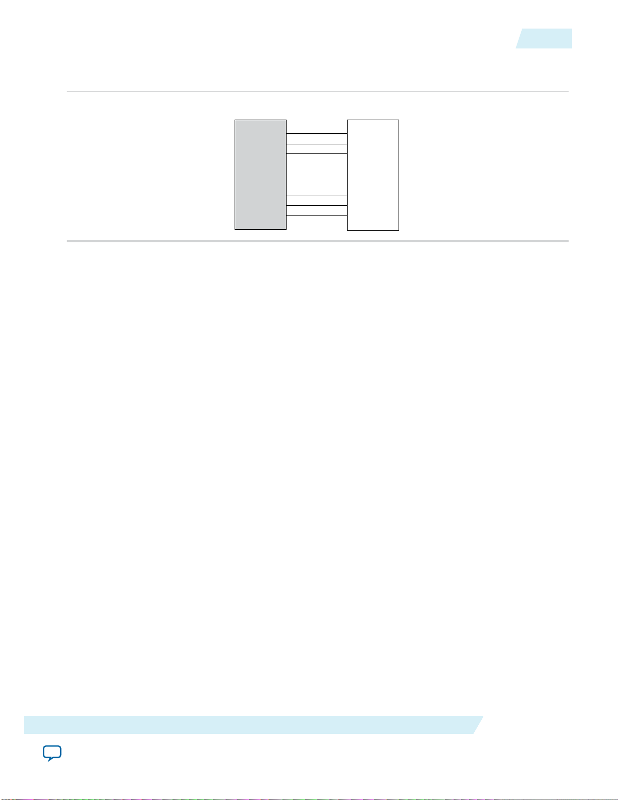
quartus - Contains the Quartus II software
ip - Contains the Altera IP Library and third-party IP cores
altera - Contains the Altera IP Library source code
<IP core name> - Contains the IP core source files
www.altera.com
101 Innovation Drive, San Jose, CA 95134
Parallel Flash Loader IP Core User Guide
UG-01082
Subscribe
Send Feedback
This document describes how to instantiate the Parallel Flash Loader (PFL) IP core in your design,
programming flash memory, and configuring your FPGA from the flash memory.
FPGAs’ increasing density requires larger configuration storage. If your system contains a flash memory
device, you can use your flash memory as the FPGA configuration storage as well. You can use the PFL IP
core in Altera® MAX® Series (MAX II, MAX V and MAX 10 devices) or all other FPGAs to program
flash memory devices efficiently through the JTAG interface and to control configuration from the flash
memory device to the Altera FPGA.
Features
Use the PFL IP core to:
• Program Common Flash Interface (CFI) flash, quad Serial Peripheral Interface (SPI) flash, or NAND
flash memory devices with the device JTAG interface.
• Control Altera FPGA configuration from a CFI flash, quad SPI flash, or NAND flash memory device
for Arria series, Cyclone series, and Stratix series FPGA devices.
Installing and Licensing IP Cores
The Altera IP Library provides many useful IP core functions for production use without purchasing an
additional license. You can evaluate any Altera® IP core in simulation and compilation in the Quartus® II
software using the OpenCore® evaluation feature. Some Altera IP cores, such as MegaCore® functions,
require that you purchase a separate license for production use. You can use the OpenCore Plus feature to
evaluate IP that requires purchase of an additional license until you are satisfied with the functionality and
performance. After you purchase a license, visit the Self Service Licensing Center to obtain a license
number for any Altera product.
Figure 1: IP Core Installation Path
©
2015 Altera Corporation. All rights reserved. ALTERA, ARRIA, CYCLONE, ENPIRION, MAX, MEGACORE, NIOS, QUARTUS and STRATIX words and logos are
trademarks of Altera Corporation and registered in the U.S. Patent and Trademark Office and in other countries. All other words and logos identified as
trademarks or service marks are the property of their respective holders as described at www.altera.com/common/legal.html. Altera warrants performance
of its semiconductor products to current specifications in accordance with Altera's standard warranty, but reserves the right to make changes to any
products and services at any time without notice. Altera assumes no responsibility or liability arising out of the application or use of any information,
product, or service described herein except as expressly agreed to in writing by Altera. Altera customers are advised to obtain the latest version of device
specifications before relying on any published information and before placing orders for products or services.
ISO
9001:2008
Registered
Page 2

2
Device Support
Note: The default IP installation directory on Windows is <drive>:\altera\<version number>; on Linux it is
<home directory>/altera/ <version number>.
Related Information
• Altera Licensing Site
• Altera Software Installation and Licensing Manual
Device Support
This user guide focuses on implementing the PFL IP core in an Altera CPLD. The PFL IP core supports all
Altera FPGAs. You can implement the PFL IP core in an Arria®, Cyclone®, or Stratix® device family
FPGA to program flash memory or to configure other FPGAs.
Related Information
AN478: Using FPGA-Based Parallel Flash Loader with the Quartus II Software
Provides more information about using the FPGA-based PFL IP core to program a flash memory device.
Supported Flash Memory Devices
The Quartus II software generates the PFL IP core logic for the flash programming bridge and FPGA
configuration.
UG-01082
2015.01.23
Table 1: CFI Flash Memory Devices Supported by PFL IP Core
If your CFI device is not in the following table, but is compatible with an Intel or Spansion CFI flash device, Altera
recommends selecting Define CFI Flash Device in the Quartus II software.
Manufacturer Product Family Data Width Density (Megabit) Device Name
(1)(2)
8 28F800C3
16 28F160C3
C3 16
32 28F320C3
64 28F640C3
Micron
32 28F320J3
8 or 16
64 28F640J3
J3
128 28F128J3
16 256 JS29F256J3
(1)
Spansion has discontinued the Spansion S29GL-N flash memory device family. Altera does not recommend
using this flash memory device. For more information about an alternative recommendation, see related
information.
(2)
The PFL IP core supports top and bottom boot block of the flash memory devices. For Micron flash memory
devices, the PFL IP core supports top, bottom, and symmetrical blocks of flash memory devices.
Altera Corporation
Parallel Flash Loader IP Core User Guide
Send Feedback
Page 3

UG-01082
2015.01.23
Supported Flash Memory Devices
3
Manufacturer Product Family Data Width Density (Megabit) Device Name
64 28F640P30
128 28F128P30
256 28F256P30
P30 16
512 28F512P30
1000 28F00AP30
2000 28F00BP30
128 28F128P33
256 28F256P33
512 28F512P33
P33 16
640 28F640P33
1000 28F00AP33
2000 28F00BP33
256 28F256M29EW
M29EW 8 or 16
512 28F512M29EW
1000 28F00AM29EW
(1)(2)
M28W160CT
M28W160CB
16
M29W160F7
M29W160FB
M29W320E
M29W 8 or 16
32
M29W320FT
M29W320FB
M29W640F
64
M29W640G
128 M29W128G
256 M29W256G
M29DW323DT
M29DW 8 or 16 32
M29DW323DB
(1)
Spansion has discontinued the Spansion S29GL-N flash memory device family. Altera does not recommend
using this flash memory device. For more information about an alternative recommendation, see related
information.
(2)
The PFL IP core supports top and bottom boot block of the flash memory devices. For Micron flash memory
devices, the PFL IP core supports top, bottom, and symmetrical blocks of flash memory devices.
Parallel Flash Loader IP Core User Guide
Send Feedback
Altera Corporation
Page 4

4
Supported Flash Memory Devices
UG-01082
2015.01.23
Manufacturer Product Family Data Width Density (Megabit) Device Name
512 MT28GU512AAA1E
GC-0SIT
G18 16
1024 MT28GU01GAAA1E
GC-0SIT
M58BW16FT
16
32
M58BW16FB
M58BW
32 M58BW32FT
16 or 32 32 M58BW32FB
128 S29GL128P
GL-P
(3)
8 or 16
256 S29GL256P
512 S29GL512P
1024 S29GL01GP
16 S29AL016D
AL-D 8 or 16
32 S29AL032D
AL-J 8 or 16 16 S29AL016J
Spansion
AL-M 8 or 16 16 S29AL016M
(1)(2)
JL-H 8 or 16
32 S29JL032H
64 S29JL064H
WS-N 16 128 S29WS128N
128 S29GL128S
256 S29GL256S
GL-S 16
512 S29GL512S
1024 S29GL01GS
16 MX29LV160D
32 MX29LV320D
MX29LV 16
MX29LV640D
Macronix
64
MX29LV640E
128 MX29GL128E
MX29GL 16
256 MX29GL256E
(1)
Spansion has discontinued the Spansion S29GL-N flash memory device family. Altera does not recommend
using this flash memory device. For more information about an alternative recommendation, see related
information.
(2)
The PFL IP core supports top and bottom boot block of the flash memory devices. For Micron flash memory
devices, the PFL IP core supports top, bottom, and symmetrical blocks of flash memory devices.
(3)
Supports page mode.
Altera Corporation
Parallel Flash Loader IP Core User Guide
Send Feedback
Page 5
UG-01082
2015.01.23
Supported Flash Memory Devices
5
Manufacturer Product Family Data Width Density (Megabit) Device Name
EN29LV 16 16 EN29LV160B
Eon Silicon
Solution
EN29GL 16
32 EN29LV320B
128 EN29GL128
Table 2: Quad SPI Flash Memory Device Supported by PFL IP Core
Manufacturer Product Family Density (Megabit) Device Name
N25Q 1.8V
Micron
128 N25Q128
N25Q 3.3V
32 S25FL032P
Spansion FL-P
64 S25FL064P
128 S25FL129P
(1)(2)
(1)
Spansion has discontinued the Spansion S29GL-N flash memory device family. Altera does not recommend
using this flash memory device. For more information about an alternative recommendation, see related
information.
(2)
The PFL IP core supports top and bottom boot block of the flash memory devices. For Micron flash memory
devices, the PFL IP core supports top, bottom, and symmetrical blocks of flash memory devices.
Parallel Flash Loader IP Core User Guide
Send Feedback
Altera Corporation
Page 6
6
Supported Flash Memory Devices
Manufacturer Product Family Density (Megabit) Device Name
UG-01082
2015.01.23
Macronix
MX25L
8
16
32
64
128
MX25L8035E
MX25L8036E
MX25L1635D
MX25L1635E
MX25L1636D
MX25L1636E
MX25L3225D
MX25L3235D
MX25L3235D
MX25L3236D
MX25L3237D
MX25L6436E
MX25L6445E
MX25L6465E
MX25L12836E
MX25L12845E
256
8
MX25U
16 MX25U1635E
32 MX25U3235E
64 MX25U6435E
Table 3: NAND Flash Memory Device Supported by PFL IP Core
Manufacturer Density (Megabit) Device Name
NAND512 1.8V
NAND512 3.0V
Micron 512
NAND512 3.3V
Micron(MT29)
Samsung 512 K9F1208R0C
MX25L12865E
MX25L25635E
MX25L25735E
MX25U8035
MX25U8035E
Toshiba 1000 TC58DVG02A1
Hynix 512 HY27US0812(1/2)B
Altera Corporation
Parallel Flash Loader IP Core User Guide
Send Feedback
Page 7

UG-01082
2015.01.23
Related Information
Spansion Website
Supported Schemes and Features
The PFL IP core allows you to configure the FPGA in passive serial (PS) or fast passive parallel (FPP)
scheme. The PFL IP core supports configuration with FPGA on-chip data compression and data
encryption.
When you use compressed or encrypted configuration data for FPP configuration, the PFL IP core holds
one data byte for one, two, four, or eight DCLK cycles to ensure the DCLK frequency runs at the required
data rate as specified by the DCLK-to-DATA[] Ratio. The PFL IP core checks if the compression or
encryption feature is turned on in the configuration image before configuring in FPP mode. Hence, no
additional setting is required in the PFL IP core to specify whether the configuration file stored in the
flash memory device is a compressed or uncompressed image.
Note: When you turn on the enhanced bitstream compression feature, data encryption is disabled.
Supported Schemes and Features
7
You can program the Altera CPLDs and flash memory device in Programmer Object File (.pof), Jam
Standard Test and Programming Language (STAPL) Format File (.jam), or JAM Byte Code File (.jbc) file
format. The PFL IP core does not support Raw Binary File (.rbf) format.
Logic element (LE) usage varies with different PFL IP core and Quartus II software settings. To determine
the exact LE usage number, compile a PFL design with your settings using the Quartus II software.
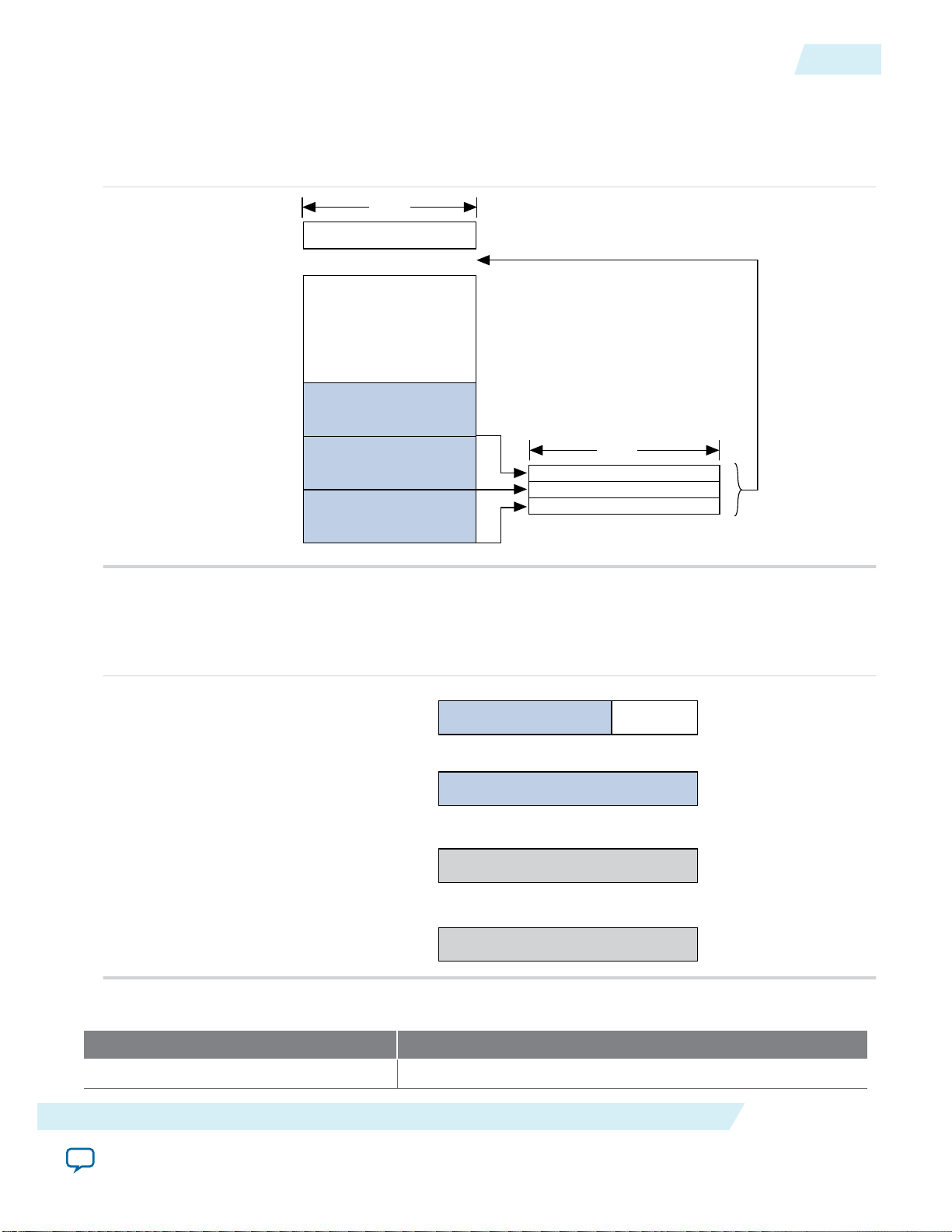
IP Catalog and Parameter Editor
The Quartus II IP Catalog (Tools > IP Catalog) and parameter editor help you easily customize and
integrate IP cores into your project. You can use the IP Catalog and parameter editor to select, customize,
and generate files representing your custom IP variation.
Note:
The IP Catalog lists IP cores available for your design. Double-click any IP core to launch the parameter
editor and generate files representing your IP variation. The parameter editor prompts you to specify an
IP variation name, optional ports, and output file generation options. The parameter editor generates a
top-level Qsys system file (.qsys) or Quartus II IP file (.qip) representing the IP core in your project. You
can also parameterize an IP variation without an open project.
Use the following features to help you quickly locate and select an IP core:
The IP Catalog (Tools > IP Catalog) and parameter editor replace the MegaWizard™ Plug-In
Manager for IP selection and parameterization, beginning in Quartus II software version 14.0. Use
the IP Catalog and parameter editor to locate and paramaterize Altera IP cores.
™
• Filter IP Catalog to Show IP for active device family or Show IP for all device families.
• Search to locate any full or partial IP core name in IP Catalog. Click Search for Partner IP, to access
partner IP information on the Altera website.
• Right-click an IP core name in IP Catalog to display details about supported devices, open the IP core's
installation folder, andor view links to documentation.
Parallel Flash Loader IP Core User Guide
Send Feedback
Altera Corporation
Page 8
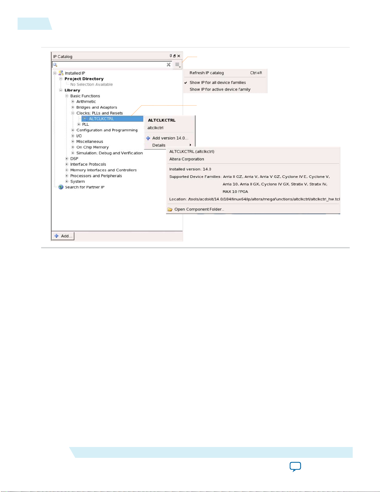
Search and filter IP for your target device
Double-click to customize, right-click for information
8
Using the Parameter Editor
Figure 2: Quartus II IP Catalog
UG-01082
2015.01.23
Note: The IP Catalog is also available in Qsys (View > IP Catalog). The Qsys IP Catalog includes
exclusive system interconnect, video and image processing, and other system-level IP that are not
available in the Quartus II IP Catalog. For more information about using the Qsys IP Catalog, refer
to Creating a System with Qsys in the Quartus II Handbook.
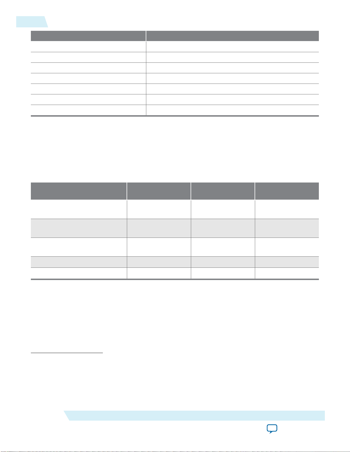
Using the Parameter Editor
The parameter editor helps you to configure IP core ports, parameters, and output file generation options.
• Use preset settings in the parameter editor (where provided) to instantly apply preset parameter values
for specific applications.
• View port and parameter descriptions, and links to documentation.
• Generate testbench systems or example designs (where provided).
Altera Corporation
Parallel Flash Loader IP Core User Guide
Send Feedback
Page 9
View IP port
and parameter
details
Apply preset parameters for
specific applications
Specify your IP variation name
and target device
Legacy parameter
editors
UG-01082
2015.01.23
Figure 3: IP Parameter Editors
Functional Description
9
Functional Description
The PFL IP core allows you to program flash memory devices with Altera CPLDs through the JTAG
interface and provides the logic to control configuration from the flash memory device to the Altera
FPGA.
Programming Flash Memory
You can use the PFL IP core to program the following flash memory devices with JTAG interface:
• Programming CFI Flash
• Programming Quad SPI Flash
• Programming NAND Flash
Related Information
• Supported Flash Memory Devices on page 2
• Third-party Programmer Support on page 39
Provides more information about programming the flash memory using third-party tools.
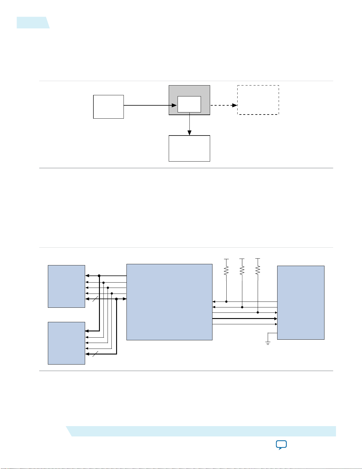
Programming CFI Flash
Altera configuration devices support programming through the JTAG interface to allow in-system
programming and updates. However, standard flash memory devices do not support the JTAG interface.
You can use the JTAG interface in Altera CPLDs to indirectly program the flash memory device.
Parallel Flash Loader IP Core User Guide
Send Feedback
The Altera CPLD JTAG block interfaces directly with the logic array in a special JTAG mode. This mode
brings the JTAG chain through the logic array instead of the Altera CPLD boundary-scan cells (BSCs).
Altera Corporation
Page 10
Altera CPLD
CFI Flash
Memory
Altera
FPGA
Configuration Data
Common
Flash
Interface
PFL
Quartus II
Software
via JTAG
Altera FPGA Not Used
for Flash Programming
V
CC
V
CC
V
CC
P30/P33 CFI Flash
Altera CPLD
Altera FPGA
P30/P33 CFI Flash
16
16
10kΩ
10kΩ
10kΩ
ADDR[24..0]
NCE
NWE
NOE
DATA[15..0]
ADDR[24..0]
NCE
NWE
NOE
DATA[15..0]
flash_addr[24..0]
flash_nce
flash_nwe
flash_noe
flash_data[31..0]
fpga_conf_done
fpga_nstatus
fpga_nconfig
fpga_data
fpga_dclk
CONF_DONE
nSTATUS
nCONFIG
DATA
nCE
DCLK
10
Programming Quad SPI Flash
The PFL IP core provides JTAG interface logic to convert the JTAG stream provided by the Quartus II
software and to program the CFI flash memory devices connected to the CPLD I/O pins.
Figure 4: Programming the CFI Flash Memory With the JTAG Interface
Figure shows an Altera CPLD configured as a bridge to program the CFI flash memory device through the
JTAG interface.
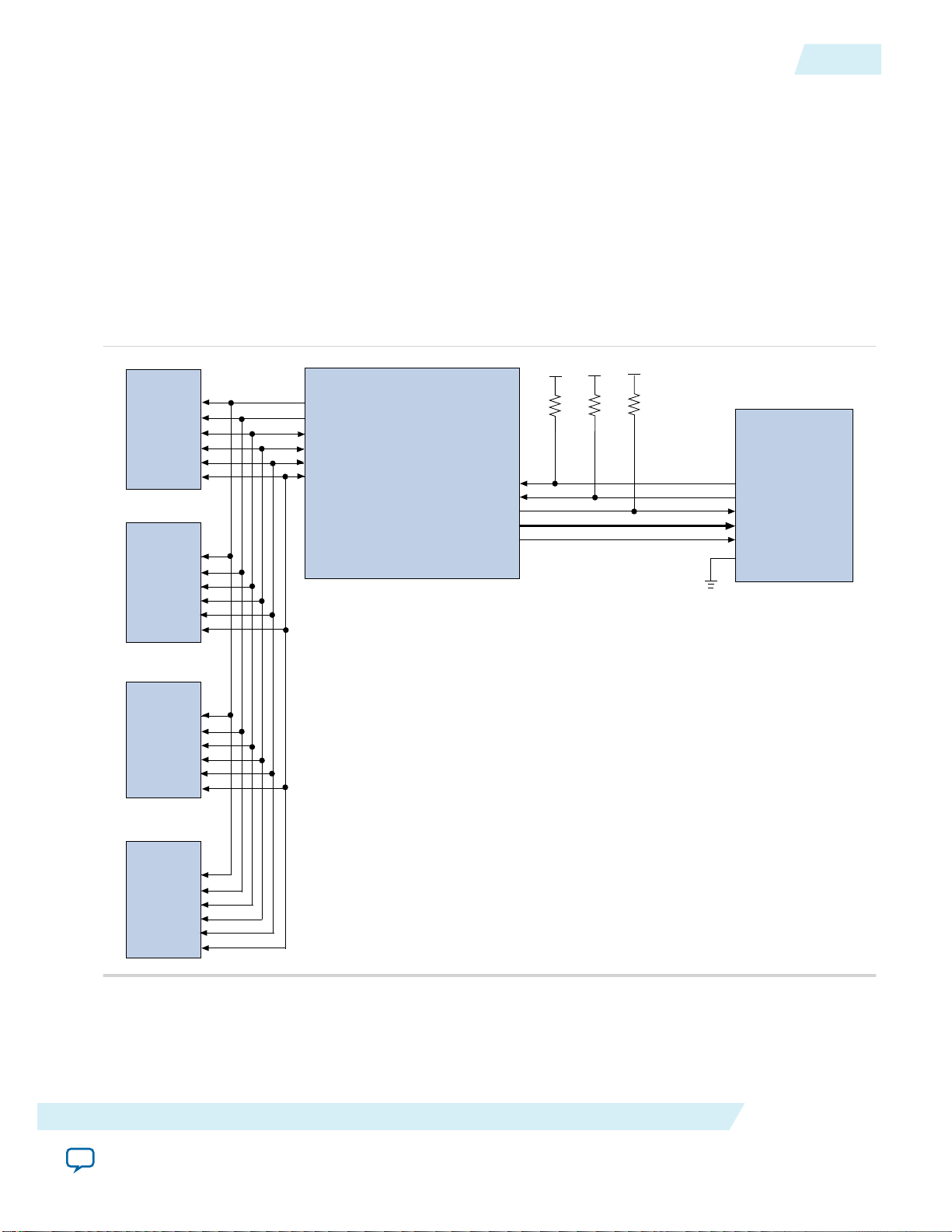
The PFL IP core supports dual P30 or P33 CFI flash memory devices in burst read mode to achieve faster
configuration time. Two identical P30 or P33 CFI flash memory devices connect to the CPLD in parallel
using the same data bus, clock, and control signals. During FPGA configuration, the FPGA DCLK
frequency is four times faster than the flash_clk frequency.
UG-01082
2015.01.23
Altera Corporation
Figure 5: PFL IP core With Dual P30 or P33 CFI Flash Memory Devices
The flash memory devices in the dual P30 or P33 CFI flash solution must have the same memory density
from the same device family and manufacturer. In the Quartus II software version 9.1 SP1 onwards, dual
P30 or P33 flash support is available in the PFL IP core.
Programming Quad SPI Flash
You can also use the JTAG interface in Altera CPLDs to program a quad SPI flash memory device with
the PFL IP core.
Parallel Flash Loader IP Core User Guide
Send Feedback
Page 11
V
CC
V
CC
V
CC
Quad SPI Flash
Altera CPLD
Altera FPGA
10kΩ
10kΩ
10kΩ
flash_sck
flash_io0
flash_io1
flash_io2
flash_io3
flash_sck[3..0]
flash_io0[3..0]
flash_io1[3..0]
flash_io2[3..0]
flash_io3[3..0]
fpga_conf_done
fpga_nstatus
fpga_nconfig
fpga_data
fpga_dclk
CONF_DONE
nSTATUS
nCONFIG
DATA
nCE
DCLK
flash_ncs
flash_ncs[3..0]
Quad SPI Flash
flash_sck
flash_io0
flash_io1
flash_io2
flash_io3
flash_ncs
Quad SPI Flash
flash_sck
flash_io0
flash_io1
flash_io2
flash_io3
flash_ncs
Quad SPI Flash
flash_sck
flash_io0
flash_io1
flash_io2
flash_io3
flash_ncs
UG-01082
2015.01.23
Programming Quad SPI Flash
The PFL IP core instantiated in the Altera CPLD functions as a bridge between the CPLD JTAG program‐
ming interface and the quad SPI flash memory device interface that connects to the Altera CPLD I/O pins.
You can connect up to four identical quad SPI flashes in parallel to implement more configuration data
storage.
Note: When connecting quad SPI flashes in parallel, use identical flash memory devices with the same
memory density from the same device family and manufacturer. In the Quartus II software version
10.0 onwards, quad SPI flash support is available in the PFL IP core.
Figure 6: Programming Quad SPI Flash Memory Devices With the CPLD JTAG Interface
Figure shows an Altera CPLD functioning as a bridge to program the quad SPI flash memory device
through the JTAG interface. The PFL IP core supports multiple quad SPI flash programming of up to four
devices.
11
Related Information
Supported Flash Memory Devices on page 2
Parallel Flash Loader IP Core User Guide
Altera Corporation
Send Feedback
Page 12
Altera CPLD
NAND Flash
Memory
Altera
FPGA
Configuration Data
Open NAND
Flash
Interface
PFL
Quartus II
Software
using JTAG
Altera FPGA Not Used
for Flash Programming
Altera CPLD
Flash
Memory
Altera
FPGA
Flash
Interface
PFL
Passive Serial or
Fast Passive Parallel
Interface
12
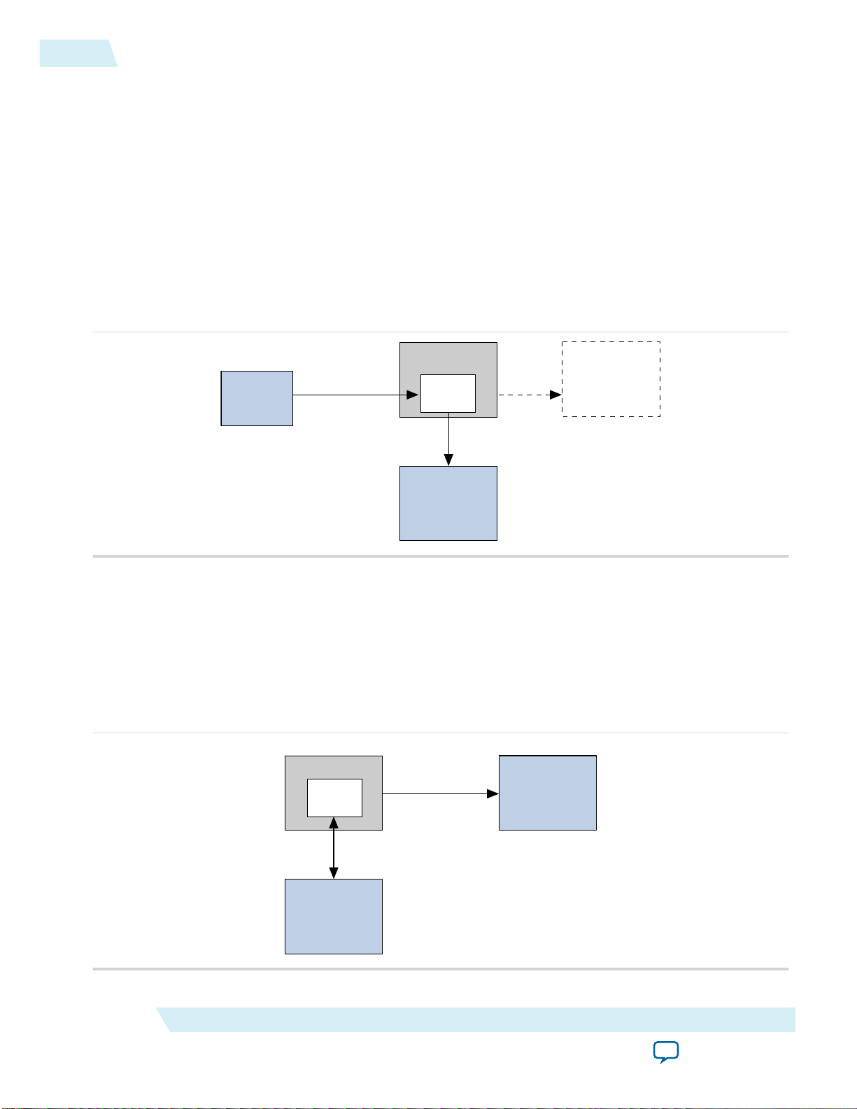
Programming NAND Flash
Programming NAND Flash
You can use the JTAG interface in Altera CPLDs to program the NAND flash memory device with the
PFL IP core. The NAND flash memory device is a simpler device that has faster erase and write speed with
higher memory density in comparison with the CFI flash.
You can use the JTAG interface in Altera CPLDs to indirectly program the flash memory device. The
CPLD JTAG block interfaces directly with the logic array in a special JTAG mode. This mode brings the
JTAG chain through the logic array instead of the Altera CPLD BSCs. The PFL IP core provides JTAG
interface logic to convert the JTAG stream from the Quartus II software and to program the NAND flash
memory device that connects to the CPLD I/O pins.
Figure 7: Programming NAND Flash Memory Devices With the JTAG Interface
Figure shows an Altera CPLD functioning as a bridge to program the NAND flash memory device
through the JTAG interface.
UG-01082
2015.01.23
Controlling Altera FPGA Configuration from Flash Memory
Altera Corporation
You can use the PFL logic in Altera CPLDs as a configuration controller for FPGA configuration. The PFL
logic in the CPLD determines when to start the configuration process, read the data from the flash
memory device, and configure the Altera FPGA in PS or FPP configuration scheme.
Figure 8: FPGA Configuration With Flash Memory Data
Figure shows the Altera CPLD as the configuration controller for the FPGA. The flash memory includes
CFI, quad SPI and NAND flash.
Parallel Flash Loader IP Core User Guide
Send Feedback
Page 13

UG-01082
2015.01.23
Mapping PFL and Flash Address
You can use the PFL IP core to either program the flash memory devices, configure your FPGA, or both;
however, to perform both functions, create separate PFL functions if any of the following conditions apply
to your design:
• You want to use fewer LEs.
• You modify the flash data infrequently.
• You have JTAG or In-System Programming (ISP) access to the Altera CPLD.
• You want to program the flash memory device with non-Altera data. For example, the flash memory
device contains initialization storage for an ASSP. You can use the PFL IP core to program the flash
memory device with the initialization data and also create your own design source code to implement
the read and initialization control with the CPLD logic.
Creating Separate PFL Functions
To create separate PFL functions, follow these steps:
1. To create a PFL instantiation, select Flash Programming Only mode.
2. Assign the pins appropriately.
3. Compile and generate a .pof for the flash memory device. Ensure that you tri-state all unused I/O pins.
4. To create another PFL instantiation, select Configuration Control Only mode.
5. Instantiate this configuration controller into your production design.
6. Whenever you must program the flash memory device, program the CPLD with the flash memory
device .pof and update the flash memory device contents.
7. Reprogram the CPLD with the production design .pof that includes the configuration controller.
13
Note:
All unused pins are set to ground by default. When programming the configuration flash memory
device through the CPLD JTAG pins, you must tri-state the FPGA configuration pins common to
the CPLD and the configuration flash memory device. You can use the
pfl_flash_access_request and pfl_flash_access_granted signals of the PFL block to tri-state
the correct FPGA configuration pins.
Related Information
• Mapping PFL and Flash Address on page 13
• Implementing Page in the Flash .pof on page 15
• Using Enhanced Bitstream Compression and Decompression on page 18
• Using Remote System Upgrade on page 20
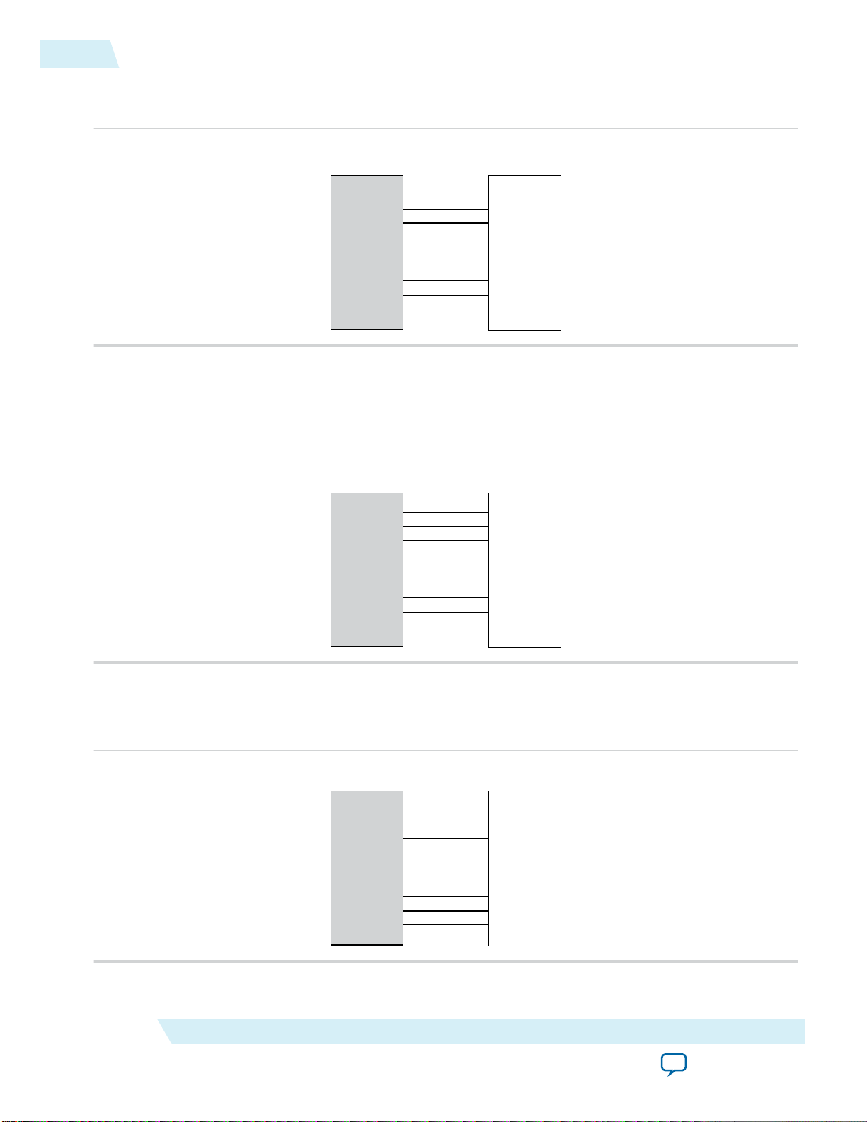
Mapping PFL and Flash Address
The address connections between the PFL IP core and the flash memory device vary depending on the
flash memory device vendor and data bus width.
Parallel Flash Loader IP Core User Guide
Send Feedback
Altera Corporation
Page 14
23
22
21
-
-
2
1
0
PFL
address: 24 bits
23
22
21
-
-
2
1
0
Flash Memory
address: 24 bits
22
21
20
-
-
2
1
0
PFL
address: 23 bits
23
22
21
-
-
3
2
1
Flash Memory
address: 23 bits
23
22
21
-
-
2
1
0
PFL
address: 24 bits
22
21
20
-
-
1
0
D15
Flash Memory
address: 24 bits
14
Mapping PFL and Flash Address
Figure 9: Micron J3 Flash Memory in 8-Bit Mode
The address connection between the PFL IP core and the flash memory device are the same.
Figure 10: Micron J3, P30, and P33 Flash Memories in 16-Bit Mode
The flash memory addresses in Micron J3, P30, and P33 16-bit flash memory shift one bit down in
comparison with the flash addresses in the PFL IP core. The flash address in the Micron J3, P30, and P33
flash memory starts from bit 1 instead of bit 0.
UG-01082
2015.01.23
Altera Corporation
Figure 11: Spansion and Micron M28, M29 Flash Memory in 8-Bit Mode
The flash memory addresses in Spansion 8-bit flash shifts one bit up. Address bit 0 of the PFL IP core
connects to data pin D15 of the flash memory.
Parallel Flash Loader IP Core User Guide
Send Feedback
Page 15
22
21
20
-
-
2
1
0
PFL
address: 23 bits
22
21
20
-
-
2
1
0
Flash Memory
address: 23 bits
UG-01082
2015.01.23
Figure 12: Spansion and Micron M28, M29 Flash Memory in 16-Bit Mode
The address bit numbers in the PFL IP core and the flash memory device are the same.
Implementing Page in the Flash .pof
The PFL IP core stores configuration data in a maximum of eight pages in a flash memory block. Each
page holds the configuration data for a single FPGA chain. A single FPGA chain can contain more than
one FPGA. For an FPGA chain with multiple FPGAs, the PFL IP core stores multiple SRAM Object Files
(.sof) in the same page.
Implementing Page in the Flash .pof
15
The total number of pages and the size of each page depends on the density of the flash. These pages allow
you to store designs for different FPGA chains or different designs for the same FPGA chain in different
pages.
Use the generated .sof files to create a flash memory device .pof. When converting these .sof files to a .pof,
use the following address modes to determine the page address:
• Block mode—Allows you to specify the start and end addresses for the page.
• Start mode—Allows you to specify only the start address. You can locate the start address for each page
on an 8-KB boundary. If the first valid start address is 0×000000, the next valid start address is an
increment of 0×2000.
• Auto mode—Allows the Quartus II software to automatically determine the start address of the page.
The Quartus II software aligns the pages on a 128-KB boundary; for example, if the first valid start
address is 0×000000, the next valid start address is an increment of 0×20000.
Note:
If you are programming NAND flash, you must specify the NAND flash memory device reserved
block start address and the start address to ensure the files reside within a 128-KB boundary
Storing Option Bits
The PFL IP core requires you to allocate space in the flash memory device for option bits. The option bits
sector contains information about the start address for each page, the .pof version used for flash
programming, and the Page-Valid bits. You must specify the options bits sector address in the flash
memory device when converting the .sof files to a .pof and creating a PFL design.
Parallel Flash Loader IP Core User Guide
Send Feedback
Altera Corporation
Page 16

16
Storing Option Bits
UG-01082
2015.01.23
Table 4: Option Bits Sector Format
Offset address 0x80 stores the .pof version required for programming flash memory. This .pof version applies to all
eight pages of the configuration data. The PFL IP core requires the .pof version to perform a successful FPGA
configuration process.
Sector Offset Value
0x00–0x03 Page 0 start address
0x04–0x07 Page 1 start address
0x08–0x0B Page 2 start address
0x0C–0x0F Page 3 start address
0x10–0x13 Page 4 start address
0x14–0x17 Page 5 start address
0x18–0x1B Page 6 start address
0x1C–0x1F Page 7 start address
0x20–0x7F Reserved
(4)
0x80
.pof version
0x81–0xFF Reserved
The Quartus II Convert Programming File tool generates the information for the .pof version when you
convert the .sof files to .pof files.
The value for the .pof version generated by the Quartus II software version 7.1 onwards is 0x03. However,
if you turn on the enhanced bitstream-compression feature, the value for the .pof version is 0x04.
Caution:
Do not overwrite any information in the option bits sector to prevent the PFL IP core from
malfunctioning, and always store the option bits in unused addresses in the flash memory
device.
(4)
.pof version occupies only one byte in the option bits sector.
Altera Corporation
Parallel Flash Loader IP Core User Guide
Send Feedback
Page 17
Option Bits
Configuration Data (Page 2)
Configuration Data (Page 1)
Configuration Data (Page 0)
Page 2 Address + Page-Valid
Page 1 Address + Page-Valid
Page 0 Address + Page-Valid
End Address
0x000000
8 Bits
32 Bits
Page Start Address [19:13] Page-Valid
Bit 7...Bit 1 Bit 0
Page Start Address [27:20]
Bit 7...Bit 0
0x002000
0x002001
Page End Address [19:13]
Bit 7...Bit 1
0x002002
Page End Address [27:20]
Bit 7...Bit 0
0x002003
(For flash byte addressing mode)
UG-01082
2015.01.23
Storing Option Bits
Figure 13: Implementing Page Mode and Option Bits in the CFI Flash Memory Device
• The end address depends on the density of the flash memory device. For the address range for devices
with different densities, refer Byte Address Range table.
• You must specify the byte address for the option bits sector.
17
Figure 14: Page Start Address, End Address, and Page-Valid Bit Stored as Option Bits
Bits 0 to 12 for the page start address are set to zero and are not stored as option bits. The Page-Valid bits
indicate whether each page is successfully programmed. The PFL IP core programs the Page-Valid bits
after successfully programming the pages.
Table 5: Byte Address Range for CFI Flash Memory Devices with Different Densities
Parallel Flash Loader IP Core User Guide
Send Feedback
CFI Device (Megabit) Address Range
8 0x0000000–0x00FFFFF
Altera Corporation
Page 18
18
Using Enhanced Bitstream Compression and Decompression
CFI Device (Megabit) Address Range
16 0x0000000–0x01FFFFF
32 0x0000000–0x03FFFFF
64 0x0000000–0x07FFFFF
128 0x0000000–0x0FFFFFF
256 0x0000000–0x1FFFFFF
512 0x0000000–0x3FFFFFF
1024 0x0000000–0x7FFFFFF
Using Enhanced Bitstream Compression and Decompression
The enhanced bitstream compression and decompression feature in the PFL IP core reduces the size of
the configuration file in the flash memory device. On average, you can reduce the file size by as much as
50% depending on the designs. When you turn on the enhanced bitstream compression feature, the PFL
IP core disables data encryption.
Table 6: Comparison Between Typical, Enhanced, and Double Compression
UG-01082
2015.01.23
FPGA Configuration Typical Bitstream
Compression Feature
FPGA on-chip bitstream
Yes No Yes
Enhanced Bitstream
Compression Feature
Double Compression
Technique
decompression enabled
PFL enhanced bitstream
No Yes Yes
decompression enabled
Typical configuration file size
35%–55% 45%–75% 40%–60%
reduction
(6)
(5)
Slow Moderate
Very fast
(7)
Not supported
PS configuration time Moderate
FPP configuration time Fast
Note: When using the PFL with compression, set the device MSEL pins set for compression or
decompression. When generating or converting a programming file, you can enable compression.
In the first few bytes during the generation of the programming file (with compression enabled), a
bit set notifies the PFL that the incoming files is a compressed file. The ×4 DCLK-to-data are
handled automatically in the PFL.
Note: For more information about the typical data compression feature, refer to the Configuration Data
Decompression section in the configuration chapter of the relevant device handbook.
(5)
(5)
The FPGA receives compressed bitstream which decreases the duration to transmit the bitstream to the
FPGA.
(6)
For FPP with on-chip bitstream decompression enabled, the DCLK frequency is ×2, ×4, or ×8 the data rate,
depending on the device. You can check the relationship of the DCLK and data rate in the FPP
Configuration section in the configuration chapter of the respective device handbook.
(7)
For FPP with enhanced bitstream decompression enabled, the DCLK frequency is ×1 the data rate.
Altera Corporation
Parallel Flash Loader IP Core User Guide
Send Feedback
Page 19

Altera CPLD
CFI or Quad SPI
Flash Memory
Altera
FPGA
PFL with
Enhanced
Bitstream
Decompression
Feature
Compressed Data
Passive Serial or
Fast Passive Parallel With
Uncompressed Data
Altera CPLD
CFI or Quad SPI
Flash Memory
PFL with
Enhanced
Bitstream
Decompression
Feature
Double Compressed
Data
Passive Serial With
Compressed Data
Altera FPGA
On-Chip
Bitstream
Decompression
Feature
UG-01082
2015.01.23
Using Enhanced Bitstream Compression and Decompression
19
For the FPP configuration scheme, the enhanced bitstream compression feature helps achieve higher
configuration data compression ratio and faster configuration time. For the PS configuration scheme, the
double compression technique helps achieve higher configuration data compression ratio and moderate
configuration time. To enable the double compression technique, turn on both the typical bitstream
compression feature and the enhanced bitstream compression feature in the PFL parameter editor.
Figure 15: FPGA Configuration Data Flow with Enhanced Bitstream Compression Feature in PS or FPP
Configuration Scheme
Figure 16: FPGA Configuration Data Flow with Double Compression Technique in PS Configuration
Scheme
Note:
The enhanced bitstream compression and decompression feature is available in the PFL IP core in
the Quartus II software version 10.0 onwards.
Parallel Flash Loader IP Core User Guide
Send Feedback
Altera Corporation
Page 20

Altera CPLD
CFI Flash
Memory
Altera
FPGA
Configuration Data
Common
Flash
Interface
PFL
Quartus II
Software
via JTAG
Altera FPGA Not Used
for Flash Programming
20
Using Remote System Upgrade
Using Remote System Upgrade
When you instantiate the PFL IP core in the Altera CPLD for FPP or PS configuration, you can use the
features in the PFL IP core to perform remote system upgrade.
You can download a new configuration image from a remote location, store it in the flash memory device,
and direct the PFL IP core to trigger an FPGA reconfiguration to load the new configuration image. You
must store each configuration image as a new page in the flash memory device. The PFL IP core supports
a maximum of eight pages.
When using remote system upgrade, the configuration images are classified as a factory image or as
application images. A factory image is a user-defined fall-back or safe configuration that performs system
recovery when unintended errors occur during or after application image configuration. The factory
image is written to the flash memory device only once by the system manufacturer and you must not
modify or overwrite the factory image. Application images implement user-defined functionality in the
target FPGA and you can remotely update in the system.
Figure 17: Remote System Upgrade Implementation with the PFL IP Core in FPP and PS Configuration
Scheme
UG-01082
2015.01.23
Remote System Upgrade State Machine in the PFL IP Core
Altera Corporation
After FPGA powers up, you have the flexibility to determine whether a factory image or any application
image is to be loaded by setting the fpga_pgm[2..0] input pin to the page in which the intended
configuration image is stored.
If an error occurs while loading the configuration image, the PFL IP core triggers a reconfiguration to
automatically load the factory image. After the FPGA successfully loads the configuration image, the
FPGA enters user mode. After the FPGA enters user mode, you can initiate a reconfiguration to a new
page by following these steps:
1. Set the fpga_pgm[2.0] input pin.
2. Release the pfl_nreset to high if the pfl_nreset is asserted to low.
3. After four or five clock cycles, pulse the pfl_nreconfigure input pin to low.
4. Ensure that all transition is synchronized to pfl_clk.
Parallel Flash Loader IP Core User Guide
Send Feedback
Page 21

Application 1
Configuration
Power-up
Factory
Configuration
Application n
Configuration
fpga_pgm[2..0] is set to
factory page
Set fpga_pgm[2..0] to
intended page and pulse
pfl_nreconfig
fpga_pgm[2..0] is set to
application 1 page
Configuration Error
Configuration Error
Configuration Error
fpga_pgm[2..0] is set to
application n page
Set fpga_pgm[2..0] to
intended page and pulse
pfl_nreconfig
Set fpga_pgm[2..0] to
intended page and pulse
pfl_nreconfig
UG-01082
2015.01.23
Remote System Upgrade State Machine in the PFL IP Core
Figure 18: Transitions Between Different Configurations in Remote System Upgrade
• The remote system upgrade feature in the PFL IP core does not restrict the factory image to page 0, but
allows the factory image to be located on other pages in the flash.
• You can load the FPGA with either a factory image or any application image after power up,
depending on the fpga_pgm[2..0] setting.
21
Note: The PFL IP core can implement a Last Revision First programming order. The application image is
updated with remote system upgrade capabilities. If a flash programming error causes the FPGA
configuration to fail, the FPGA is reconfigured from the factory image address. A system shipped
from the factory has the same configuration file at the application image address and the factory
Parallel Flash Loader IP Core User Guide
Send Feedback
Altera Corporation
Page 22

FlashWatchdog
timer reset
circuitry
Altera FPGA
Image
update
circuitry
Remote Host
PFL
Watchdog timer reset
User logic
FPP or PS
configuration
pfl_nreconfigure
fpga_pgm[2..0]
Altera CPLD
22
Implementing Remote System Upgrade with the PFL IP Core
image address. Altera recommends that you write-protect the factory image blocks in the flash
memory device.
Implementing Remote System Upgrade with the PFL IP Core
You can achieve the remote system upgrade capabilities with the PFL IP core by controlling the
fpga_pgm[2..0] and the pfl_nreconfigure ports.
To control the fpga_pgm[2..0] and the pfl_nreconfigure ports, user-defined logic must perform the
following capabilities:
• After FPGA power up, user logic sets the fpga_pgm[2..0] ports to specify which page of configuration
image is to be loaded from the flash.
• After the remote host completes the new image update to the flash, user logic triggers a reconfigura‐
tion by pulling the pfl_nreconfigure pin low and setting the fpga_pgm[2..0] to the page in which
the new image is located. The pfl_nreconfigure signal pulsed low for greater than one pfl_clk
cycle.
• If you have enabled the user watchdog timer, user logic can monitor the pfl_watchdog_error port to
detect any occurrence of watchdog time-out error. If the pfl_watchdog_error pin is asserted high,
this indicates watchdog time-out error. You can use the user logic to set the fpga_pgm[2..0] and pull
the pfl_nreconfigure port low to initiate FPGA reconfiguration. The recovery page to be loaded
from the flash memory device after watchdog timer error depends on the fpga_pgm[2..0] setting.
UG-01082
2015.01.23
Figure 19: Implementation of Remote System Upgrade with the PFL IP Core
User Watchdog Timer
The user watchdog timer prevents faulty configuration from stalling the device indefinitely. The system
uses the timer to detect functional errors after a configuration image is successfully loaded into the FPGA.
The user watchdog timer is a time counter that runs at the pfl_clk frequency. The timer begins
counting after the FPGA enters user mode and continues until the timer reaches the watchdog time out
Altera Corporation
Parallel Flash Loader IP Core User Guide
Send Feedback
Page 23

Create a new MAX II design,
instantiate the PFL Megafunction in
the MAX II design, and create
Pin Assignments
Add the MAX II .pof to the
Quartus II Programmer
Add the flash .pof in the
Quartus II Programmer
Program the MAX II and Flash Devices
MAX II configures the FPGA with the
configuration data from the Flash Device
Compile and
obtain the
FPGA
.sof(s)
Convert to
.pof for the
Targeted
Flash
Compile
and obtain
MAX II
.pof
Add the .sof(s) for conversion to .pof
Create new FPGA
designs
Create the optional Jam
programming file
UG-01082
2015.01.23
period. You must periodically reset this timer by asserting the pfl_reset_watchdog pin before the
watchdog time-out period. If the timer does not reset before the watchdog time-out period, the PFL IP
core detects watchdog time-out error and initiates a reconfiguration to load the factory image.
Instantiate the watchdog timer reset circuitry in the configuration image loaded into the FPGA. Connect
one output signal from the reset circuitry to the pfl_reset_watchdog pin of the PFL in the CPLD to
periodically send a reset signal to the user watchdog timer. To reset the watchdog timer correctly, hold the
pfl_reset_watchdog pin high or low for at least two pfl_clk cycles.
Note: The user watchdog timer feature for remote system upgrade is available in the PFL IP core in the
Quartus II software version 10.0 onwards.
Using the PFL IP Core
This section describes the procedures on how to use the PFL IP core.
Figure 20: Process for Using the PFL IP Core
Figure shows the process for using the PFL IP core, using MAX II as an example.
Using the PFL IP Core
23
Parallel Flash Loader IP Core User Guide
Send Feedback
Altera Corporation
Page 24

24
Customizing and Generating IP Cores
Related Information
AN478: Using FPGA-Based Parallel Flash Loader with the Quartus II Software
Provides more information about using the FPGA-based PFL IP core to program a flash memory device.
Customizing and Generating IP Cores
You can customize IP cores to support a wide variety of applications. The Quartus II IP Catalog displays
IP cores available for the current target device. The parameter editor guides you to set parameter values
for optional ports, features, and output files.
To customize and generate a custom IP core variation, follow these steps:
1. In the IP Catalog (Tools > IP Catalog), locate and double-click the name of the IP core to customize.
The parameter editor appears.
2. Specify a top-level name for your custom IP variation. This name identifies the IP core variation files
in your project. If prompted, also specify the target Altera device family and output file HDL
preference. Click OK.
3. Specify the desired parameters, output, and options for your IP core variation:
• Optionally select preset parameter values. Presets specify all initial parameter values for specific
applications (where provided).
• Specify parameters defining the IP core functionality, port configuration, and device-specific
features.
• Specify options for generation of a timing netlist, simulation model, testbench, or example design
(where applicable).
• Specify options for processing the IP core files in other EDA tools.
4. Click Finish or Generate to generate synthesis and other optional files matching your IP variation
specifications. The parameter editor generates the top-level .qip or .qsys IP variation file and HDL files
for synthesis and simulation. Some IP cores also simultaneously generate a testbench or example
design for hardware testing.
5. To generate a simulation testbench, click Generate > Generate Testbench System. Generate >
Generate Testbench System is not available for some IP cores.
6. To generate a top-level HDL design example for hardware verification, click Generate > HDL
Example. Generate > HDL Example is not available for some IP cores.
UG-01082
2015.01.23
When you generate the IP variation with a Quartus II project open, the parameter editor automatically
adds the IP variation to the project. Alternatively, click Project > Add/Remove Files in Project to
manually add a top-level .qip or .qsys IP variation file to a Quartus II project. To fully integrate the IP
into the design, make appropriate pin assignments to connect ports. You can define a virtual pin to
avoid making specific pin assignments to top-level signals.
Note:
By default, all unused pins are tied to ground. Altera recommends setting all unused pins to tristate because doing otherwise might cause interference. To set all unused pins to tri-state, in the
Quartus II software, click Assignments > Device > Device and Pin Options > Unused Pins
and select an item from the Reserve all unused pins list.
Converting .sof Files to a .pof
To generate a programming file with different compression features, you must convert the .sof files to
a .pof.
Altera Corporation
Parallel Flash Loader IP Core User Guide
Send Feedback
Page 25

UG-01082
2015.01.23
Converting .sof Files to a .pof
25
To convert the .sof files to a .pof, follow these steps:
1. On the File menu, click Convert Programming Files.
2. For Programming file type, specify Programmer Object File (.pof) and name the file.
3. For Configuration device, select the CFI or NAND flash memory device with the correct density. For
example, CFI_32Mb is a CFI device with 32-Megabit (Mb) capacity.
4. To add the configuration data, under Input files to convert, select SOF Data.
5. Click Add File and browse to the .sof files you want to add.
You can place more than one .sof in the same page if you intend to configure a chain of FPGAs. The
order of the .sof files must follow the order of the devices in the chain.
If you want to store the data from other .sof files in a different page, click Add SOF page. Add the .sof
files to the new page.
6. Select SOF Data and click Properties to set the page number and name. Under Address mode for
selected pages, select Auto to let the Quartus II software automatically set the start address for that
page. Select Block to specify the start and end addresses, or select Start to specify the start address
only.
7. Click OK.
8. You can also store Hexadecimal (Intel-Format) File (.hex) user data in the flash memory device:
a. In the Input files to convert sub-window of the Convert Programming Files window, select Add
Hex Data.
b. In the Add Hex Data dialog box, select either absolute or relative addressing mode.
• If you select absolute addressing mode, the data in the .hex is programmed in the flash memory
device at the exact same address location listed in the .hex.
• If you select relative addressing mode, specify a start address.
The data in the .hex is programmed into the flash memory device with the specific start address, and
the differences between the addresses are kept. If no address is specified, the Quartus II software selects
an address.
Note:
You can also add other non-configuration data to the .pof by selecting the .hex that contains
your data when creating the flash memory device .pof.
9. Click Options to specify the start address to store the option bits. This start address must be identical
to the address you specify when creating the PFL IP core. Ensure that the option bits sector does not
overlap with the configuration data pages and that the start address resides on an 8-KB boundary.
10.If you are using a NAND flash memory device, specify the reserved block start address and the start
address (including the option bits) within a 128-KB boundary. To specify the address, in the File/Data
area column, select NAND flash Reserved Block and click Properties.
11.To generate programming files with either the typical or enhanced bitstream compression feature, or
both, perform one of the following steps:
Parallel Flash Loader IP Core User Guide
Send Feedback
Altera Corporation
Page 26

26
Constraining PFL Timing
UG-01082
2015.01.23
• Typical bitstream compression feature
1. Select .sof under SOF Data.
2. Click Properties, and then turn on the Compression option.
3. Click OK.
• Enhanced bitstream compression feature
1. In the Options dialog box, turn on the Enable enhanced bitstream-compression when
available option.
2. Click OK.
• Double compression technique
• Perform all the steps for the typical bitstream compression and enhanced bitstream compression
features listed above.
Note: For more information about the compression feature in the PFL IP core, refer to “Using
Enhanced Bitstream Compression and Decompression”.
12.To generate programming files with encrypted data, select .sof under SOF Data and click Properties.
Turn on the Generate encrypted bitstream check box.
13.Click OK to create the .pof.
Related Information
Using Enhanced Bitstream Compression and Decompression on page 18
Constraining PFL Timing
The PFL IP core supports the Quartus II TimeQuest Timing Analyzer for accurate timing analysis on the
Altera IP cores. To perform timing analysis, you must define the clock characteristics, external path
delays, and timing exceptions for the PFL input and output ports. This section provides guidelines for
defining this information for PFL input and output ports for use by the TimeQuest analyzer.
Note:
Note: After you specify the timing constraint settings for the clock signal and for the asynchronous and
Related Information
Quartus II TimeQuest Timing Analyzer of Quartus II Handbook
Provides more information about the TimeQuest analyzer.
Constraining Clock Signal
At any given time, one of the following two clock sources clocks the blocks and modules of the PFL IP
core:
The TimeQuest analyzer is a timing analysis tool that validates the timing performance of the logic
in the design using industry-standard constraint, analysis, and reporting methodology. For more
information about the TimeQuest analyzer, refer to the Quartus II TimeQuest Timing Analyzer
chapter in volume 3 of the Quartus II Handbook.
synchronous input and output ports in the TimeQuest analyzer, on the Constraints menu, click
Write SDC File to write all the constraints to a specific System Design Constraints File (.sdc). After
the .sdc is written, run full compilation for the PFL design.
• Clock signals from the pfl_clk ports of the PFL during FPGA configuration
• TCK pins of the JTAG programming interface during flash programming
Altera Corporation
Parallel Flash Loader IP Core User Guide
Send Feedback
Page 27

UG-01082
2015.01.23
The clock signal on the TCK pins is internally constrained to the maximum frequency supported by the
selected JTAG programming hardware. It is not necessary to constrain the clock signal.
You can constrain pfl_clk to the maximum frequency that the PFL IP core supports. You can use the
create_clock command or the Create Clock dialog box to specify the period and duty cycle of the clock
constraint.
To constrain the pfl_clk signal in the TimeQuest analyzer, follow these steps:
1.
Run full compilation for the PFL design. Ensure that the timing analysis tool is set to TimeQuest
Timing Analyzer.
2. After full compilation completes, on the Tools menu, select TimeQuest Timing Analyzer to launch
the TimeQuest analyzer window.
3. In the Tasks list, under Diagnostic, click Report Unconstrained Paths to view the list of
unconstrained parts and ports of the PFL design.
4. In the Report list, under Unconstrained Paths, click Clock Summary to view the clock that requires
constraints. The default setting for all unconstrained clocks is 1 GHz. To constrain the clock signal,
right-click the clock name and select Edit Clock Constraint.
5. In the Create Clock dialog box, set the period and the duty cycle of the clock constraint.
6. Click Run.
Constraining Synchronous Input and Output Ports
The setup and hold time of synchronous input and output ports is critical to the system designer. To
avoid setup and hold time violations, you can specify the signal delay from the FPGA or the flash memory
device to the synchronous input and output ports of the PFL IP core. The Quartus II Fitter places and
routes the input and output registers of the PFL IP core to meet the specified timing constraints.
Constraining Synchronous Input and Output Ports
27
Note:
For more information about the synchronous input and output ports of the PFL IP core, refer to
PFL Timing Constraints table.
The signal delay from FPGA or flash memory device to the PFL synchronous input port is specified by
set_input_delay. The delay calculation is:
Input delay value = Board delay from FPGA or flash output port to the PFL input port + TCO of the FPGA
or flash memory device
The signal delay from PFL synchronous output port to FPGA or flash memory device is specified by
set_output_delay. The delay calculation is:
Output delay value = Board delay from the PFL output port to the FPGA or flash input port + TSU of
FPGA or flash device.
Note:
TCO is the clock-to-output time from the timing specification in the FPGA, CPLD or flash
datasheet.
Parallel Flash Loader IP Core User Guide
Send Feedback
Altera Corporation
Page 28

28
Constraining Asynchronous Input and Output Ports
To constrain the synchronous input and output signals in the TimeQuest analyzer, follow these steps:
1.
Run full compilation for the PFL design. Ensure that the timing analysis tool is set to TimeQuest
Timing Analyzer.
2. After full compilation completes, on the Tools menu, select TimeQuest Timing Analyzer to launch
the TimeQuest analyzer window.
3. In the Tasks list, under Diagnostic, click Report Unconstrained Paths to view the list of
unconstrained parts and ports of the PFL design.
4. In the Report list, under the Unconstrained Paths category, select Setup Analysis, and then click
Unconstrained Input Port Paths.
5. Right-click each synchronous input or output port in the From list or To list and select
set_input_delay for the input port or set_output_delay for the output port, then specify the input
delay or output delay value.
Related Information
Summary of PFL Timing Constraints on page 28
Constraining Asynchronous Input and Output Ports
You can exclude asynchronous input and output ports from the timing analysis of the PFL IP core
because the signals on these ports are not synchronous to a IP core clock source. The internal structure of
the PFL IP core handles the metastability of these asynchronous signals.
UG-01082
2015.01.23
To exclude asynchronous input and output ports from the timing analysis, use the set_false_path
command to ignore these ports during timing analysis.
Note:
After you specify all timing constraint settings for the clock signal, on the Constraints menu, click
Write SDC File to write all the constraints to a specific .sdc. Then, run full compilation for the PFL
design again.
Summary of PFL Timing Constraints
Table 7: PFL Timing Constraints
Type Port Constraint Type Delay Value
Input clock pfl_clk create_clock Can be constrained up to the
maximum frequency supported
by the PFL IP core.
pfl_nreset set_false_path —
fpga_pgm set_false_path —
Input asynchro‐
nous
fpga_conf_done set_false_path —
fpga_nstatus set_false_path —
pfl_flash_access_granted set_false_path —
pfl_nreconfigure set_false_path —
Altera Corporation
Parallel Flash Loader IP Core User Guide
Send Feedback
Page 29

UG-01082
2015.01.23
Simulating PFL Design
Type Port Constraint Type Delay Value
fpga_nconfig set_false_path —
pfl_flash_access_request set_false_path —
29
Output asynchro‐
nous
Bidirectional
synchronous
Output synchro‐
nous
Simulating PFL Design
You can simulate the behavior of the PFL IP core with the ModelSim®-Altera software as it configures an
FPGA. This section provides guidelines on the PFL simulation for FPGA configuration.
Note:
PFL simulation is based on functional netlist, and does not support gate-level simulation. PFL
simulation does not reflect the true behavior of the hardware. Altera certifies the PFL IP core based
on actual hardware testing, and not through PFL simulation. The PFL simulation only provides
primitive behavioral simulation.
flash_nce set_false_path —
flash_nwe set_false_path —
flash_noe set_false_path —
flash_addr set_false_path —
flash_data
• Normal read mode:
set_false_path
• Burst read mode:
Burst read mode:
Board delay from fpga_dclk
pin of the CPLD to DCLK pin of
the FPGA
set_input_delay
fpga_data set_input_delay Board delay + T
fpga_dclk set_input_delay Board delay from fpga_dclk pin
of the FPGA
SU
of the CPLD to DCLK pin of the
FPGA
Table 8: Files Required for PFL Simulation in the ModelSim-Altera Software
File/Library Description
.vo or .vho The Verilog HDL or VHDL output file of the PFL IP core.
.sdo The Standard Delay Format Output file (.sdo) of the PFL IP core.
Simulation libraries:
• altera
The precompiled library files for Altera IP core primitives and Altera CPLDs
in the ModelSim-Altera software.
• altera_mf
• maxii
• maxv
Test bench Test bench file to establish the interface between the PFL IP core and the flash
memory device.
Flash simulation model
files
The simulation model files for the flash memory devices in the PS or FPP
configuration. For the flash simulation model file for each flash memory
device, refer to the respective flash memory device manufacturer.
Parallel Flash Loader IP Core User Guide
Send Feedback
Altera Corporation
Page 30

30
Creating a Test Bench File for PFL Simulation
Related Information
• ModelSim-Altera Software Support
Provides more information about simulation setup in ModelSim-Altera software.
• Altera Knowledge Center
Provides more information about known PFL simulation issues.
• About Using the ModelSim Software with the Quartus II Software
Provides more information about obtaining the .vo or .vho, .sdo, and simulation libraries in the
ModelSim-Altera software.
Creating a Test Bench File for PFL Simulation
You can use a test bench file to establish the interface between the PFL IP core and the flash memory
device. You must map the input and output ports of the PFL IP core to the appropriate data or address
bus, and to the control signals of the flash.
To perform the signal mapping, you must include the PFL primitive block and the flash primitive block in
the test bench. The primitive blocks contain the input and output ports of the device. You can obtain the
flash primitive blocks from the simulation model files provided by the flash memory device manufacturer.
To establish the connection between the PFL IP core and the flash memory device, you must connect the
flash data bus, the flash address bus, and the flash control signals from the PFL primitive block to the
appropriate ports of the flash primitive block.
UG-01082
2015.01.23
Example 1: PFL Primitive Block
pfl pfl_inst (
.fpga_pgm(<fpga_pgm source>),
.pfl_clk(<pfl clock source>),
.pfl_flash_access_granted(<pfl_flash_access_granted source>),
.pfl_flash_access_request(<pfl_flash_access_granted destination>),
.pfl_nreconfigure(<pfl_nreconfigure source>),
.pfl_nreset(<pfl_nreset source>),
.flash_addr(<flash address bus destination>),
.flash_data(<flash_data bus destination>),
.flash_nce(<flash_nce destination>),
.flash_noe(<flash_noe destination>),
.flash_nreset(<flash_nreset destination>),
.flash_nwe(<flash_nwe destination>),
.fpga_conf_done(<fpga_conf_done source>),
.fpga_nstatus(<fpga_nstatus source>),
.fpga_data(<fpga_data destination>),
.fpga_dclk(<fpga_dclk destination>),
.fpga_nconfig(<fpga_nconfig destination>),
);
Note:
For more information about the flash simulation model files, contact the flash memory device
manufacturer.
Performing PFL Simulation in the ModelSim-Altera Software
To perform PFL simulation in the ModelSim-Altera software, you must specify the .sdo or load the
ModelSim precompiled libraries listed in Files Required for PFL Simulation in the ModelSim-Altera
Software table.
Altera Corporation
Parallel Flash Loader IP Core User Guide
Send Feedback
Page 31

UG-01082
2015.01.23
Related Information
• Simulating PFL Design on page 29
• About Using the ModelSim Software with the Quartus II Software
Provides more information about obtaining the .vo or .vho, .sdo, and simulation libraries in the
ModelSim-Altera software.
Performing PFL Simulation for FPGA Configuration
Before beginning the FPGA configuration, the PFL IP core reads the option bits stored in the option bits
sector to obtain information about the .pof version used for flash programming, the start and end address
of each page of the configuration image stored in the flash, and the Page-Valid bit.
In this simulation example, the start and end addresses of the option bits sector are 0×800000 and
0×800080, respectively. The PFL IP core first reads from the final address, which is 0×800080, to obtain
the .pof version information. Because fpga_pgm[2..0] is set to 000, the PFL IP core reads from address
0×800000 to address 0×800003 to get the start and end address of page 0 and the Page-Valid bit. The LSB
in address 0×800000 is the Page-Valid bit.
The Page-Valid bit must be 0 for the PFL IP core to proceed with FPGA configuration. While the PFL IP
core reads from the flash, it asserts the active-low flash_nce and flash_noe signals, and asserts the
active-high pfl_flash_access_request signal.
Performing PFL Simulation for FPGA Configuration
31
Note: Before you perform the device configuration simulation, ensure that the PFL IP core receives the
correct option bits address and associated values to guarantee correct simulation output.
Figure 21: Simulation Before Configuration
Figure shows the simulation when the PFL IP core reads the option bits from the flash memory device
before configuration starts.
Parallel Flash Loader IP Core User Guide
Send Feedback
Altera Corporation
Page 32

32
Programming Altera CPLDs and Flash Memory Devices
After reading the option bits for page 0, the PFL IP core waits for a period of time before the configuration
starts. The flash_data remains at 0×ZZ within this period. Configuration starts when the fpga_dclk
starts to toggle. During configuration, the PFL IP core asserts the flash_nce and flash_noe signals low,
and the pfl_flash_access_request signal high.
Figure 22: Simulation When FPGA Configuration Starts
UG-01082
2015.01.23
The FPGA configuration continues until the fpga_conf_done signal is asserted high, which indicates the
configuration is complete. After the configuration process completes, the PFL IP core pulls the flash_nce
and flash_noe signals high and the pfl_flash_access_request signal low to indicate the configuration
data is no longer being read from the flash memory device.
Programming Altera CPLDs and Flash Memory Devices
Using the Quartus II Programmer, you can program Altera CPLDs and flash memory device in a single
step or separate steps.
To program both in a single step, first program the CPLD, then the flash memory device. Follow these
steps:
1. Open the Quartus II Programmer window and click Add File to add the .pof for the CPLD.
2. Right-click the CPLD .pof and click Attach Flash Device.
3. In the Flash Device menu, select the density of the flash memory device to be programmed.
4. Right-click the necessary flash memory device density and click Change File.
Altera Corporation
Parallel Flash Loader IP Core User Guide
Send Feedback
Page 33

UG-01082
2015.01.23
Programming Altera CPLDs and Flash Memory Devices Separately
5. Select the .pof generated for the flash memory device. The .pof for the flash memory device is attached
to the .pof of the CPLD.
6. Add other programming files if your chain has other devices.
7. Check all the boxes in the Program/Configure column for the new .pof and click Start to program the
CPLD and flash memory device.
The Quartus II Programmer allows you to program, verify, erase, blank-check, or examine the
configuration data page, the user data page, and the option bits sector separately, provided the CPLD
contains the PFL IP core.
Note: The Quartus II programmer erases the flash memory device if you select the .pof of the flash
memory device before programming. To prevent the Quartus II Programmer from erasing
other sectors in the flash memory device, select only the pages, .hex data, and option bits.
Programming Altera CPLDs and Flash Memory Devices Separately
To program the CPLD and the flash memory devices separately, follow these steps:
1. Open the Quartus II Programmer window.
2. Click Add File. The Add Programming File Window dialog box appears.
3. Add the targeted .pof, and click OK.
4. Check the boxes under the Program/Configure column of the .pof.
5. Click Start to program the CPLD.
6. After the programming progress bar reaches 100%, click Auto Detect. For example, if you are using
dual P30 or P33, the programmer window shows a dual P30 or P33 chain in your setup.
Alternatively, you can add the flash memory device to the programmer manually. Right-click the
CPLD .pof and click Select Flash Device. In the Select Flash Device dialog box, select the device of
your choice.
7. Right-click the necessary flash memory device density and click Change File.
33
Note:
You must select the density that is equivalent to the sum of the density of two CFI or NAND
flash memory devices. For example, if you require two 512-Mb CFI flash memory devices, then
select CFI 1 Gbit. For more than one quad SPI flash memory device, select the density that is
equivalent to the sum of all the density of the quad SPI flash memory devices. For example, a
four quad SPI flash memory devices (128 Mb for each device), the total density is equivalent to
512 Mb. A .pof with 512-Mb flash density is required to program these quad SPI flash devices.
The PFL IP core handles the 512-Mb .pof programming to the four quad SPI flash memory
devices.
8. Select the .pof generated for the flash memory device. The .pof for the flash memory device is attached
to the .pof of the CPLD.
9. Check the boxes under the Program/Configure column for the added .pof and click Start to program
the flash memory devices.
Defining New CFI Flash Device
The PFL IP core supports Intel-compatible and AMD-compatible flash memory devices. In addition to
the supported flash memory devices, you can define the new Intel- or AMD-compatible CFI flash
memory device in the PFL-supported flash database using the Define new CFI flash memory device
feature.
Parallel Flash Loader IP Core User Guide
Altera Corporation
Send Feedback
Page 34

34
Defining New CFI Flash Device
To add a new CFI flash memory device to the database or update a CFI flash device in the database, follow
these steps:
1. In the Programmer window, on the Edit menu, select Define New CFI Flash Device. The Define CFI
Flash Device window appears. The following table lists the three functions available in the Define CFI
Flash Device window.
Table 9: Functions of the Define CFI Flash Device Feature
Function Description
New Add new Intel- or AMD-compatible CFI flash memory device into the PFL-
supported flash database.
Edit Edit the parameters of the newly added Intel- or AMD-compatible CFI flash
memory device in the PFL-supported flash database.
Remove Remove the newly added Intel- or AMD-compatible CFI flash memory device
from the PFL-supported flash database.
2. To add a new CFI flash memory device or edit the parameters of the newly added CFI flash memory
device, select New or Edit. The New CFI Flash Device dialog box appears.
3. In the New CFI Flash Device dialog box, specify or update the parameters of the new flash memory
device. You can obtain the values for these parameters from the datasheet of the flash memory device
manufacturer.
UG-01082
2015.01.23
Table 10: Parameter Settings for New CFI Flash Device
Parameter Description
CFI flash device name Define the CFI flash name
CFI flash device ID Specify the CFI flash identifier code
CFI flash manufacturer ID Specify the CFI flash manufacturer identification number
CFI flash extended device ID Specify the CFI flash extended device identifier, only
applicable for AMD-compatible CFI flash memory device
Flash device is Intel compatible Turn on the option if the CFI flash is Intel compatible
Typical word programming time Typical word programming time value in µs unit
Maximum word programming time Maximum word programming time value in µs unit
Typical buffer programming time Typical buffer programming time value in µs unit
Maximum buffer programming time Maximum buffer programming time value in µs unit
Note: You must specify either the word programming time parameters, buffer programming time
parameters, or both. Do not leave both programming time parameters with the default value of
zero.
4. Click OK to save the parameter settings.
5. After you add, update, or remove the new CFI flash memory device, click OK.
Altera Corporation
Parallel Flash Loader IP Core User Guide
Send Feedback
Page 35

UG-01082
2015.01.23
Related Information
Supported Flash Memory Devices on page 2
Programming Multiple Flash Memory Devices
The PFL IP core supports multiple-flash programming of as many as 16 flash memory devices. This
feature allows the PFL IP core to connect to multiple flash memory devices to perform flash programming
sequentially. PFL multiple-flash programming supports both speed and area mode flash programming.
For FPGA configuration, use the content in the flash memory device that connects to the nCE[0] pin as
configuration data.
To use the multiple flash programming feature, follow these steps:
1. Select the number of flash memory devices connected to the CPLD in the PFL IP core parameter
editor.
2. Connect the nCE pins of the PFL to the nCE pins of the flash memory device in the block diagram.
Compile the design.
3. Click Auto Detect in the Quartus II programmer. The CPLD appears as the main item, followed by a
list of CFI flash memory devices detected as secondary items in the device tree.
4. Attach the flash memory device .pof to each flash memory device.
5. Check the boxes in the Quartus II Programmer for the necessary operation and click Start.
Programming Multiple Flash Memory Devices
35
Creating Jam Files for Altera CPLDs and Flash Memory Device Programming
To use .jam files to program the CPLD and flash memory device, follow these steps:
1. Open the Quartus II Programmer window and click Add File to add the .pof for the CPLD.
2. Right-click the CPLD .pof and click Attach Flash Device.
3. In the Flash Device menu, select the density of the flash memory device to be programmed.
4. Right-click the necessary flash memory device density and click Change File.
5. Select the .pof generated for the flash memory device. The .pof for the flash memory device is attached
to the .pof of the CPLD.
6. On the File menu, point to Create/Update and click Create JAM, JBC, SVF, or ISF File.
7. Enter a name and select the file format (.jam).
8. Click OK.
Note:
Related Information
Use the .jam files with the Quartus II Programmer or quartus_jli executable file.
AN425: Using the Command-Line Jam STAPL Solution for Device Programming.
Provides more information about the quartus_jli executable.
PFL IP Core In Embedded Systems
The PFL IP core allows processors, such as the Nios® II processor, to access the flash memory device
while programming flash and configuring an FPGA.
The following figure shows how you can use the PFL IP core to program the flash memory device and to
configure the FPGA with a Nios II processor. The configured Nios II processor uses the non-configura‐
tion data stored in the same flash memory device.
Parallel Flash Loader IP Core User Guide
Send Feedback
Altera Corporation
Page 36

pfl_nreset
pfl_flash_access_granted
flash_addr
flash_data
flash_nwe
flash_nce
flash_noe
pfl_flash_access_request
fpga_conf_done
fpga_nstatus
fpga_nconfig
fpga_data
fpga_dclk
nRP
nWP
ADDR
DATA
nWE
nCE
nOE
WP#/ACC
BYTE#
V
CC
10kΩ
V
CC
Altera FPGA
Altera CPLD
CFI Flash
10kΩ
V
CC
10kΩ
V
CC
V
CC
(1)
(1)
(1)
(2)
Nios II Processor Interface
(3)
(4)
flash_access_granted
ext_ram_bus_addr
ext_ram_bus_data
write_n_to_ext_flash
chip_n_to_ext_flash
output_n_to_ext_flash
WP#/ACC
BYTE#
flash_access_request
NC
CONF_DONE
nSTATUS
nCONFIG
DATA
DCLK
nCE
nCEO
You must connect the pull-up resistor to a supply that provides an acceptable input signal for the devices. VCC must be high enough to meet the VIH specification of the I/O
on both devices. For example, the Stratix II VIH specification ranges from 1.7 to 3.3 V; therefore, the supply for the pull-up resistor, VCC, must be within 1.7 to 3.3 V to meet
the VIH specification.
For PS configuration mode, this is a 1-bit data line. For FPP configuration mode, this is an 8-bit data bus.
Do not connect anything to the NC pin (the no connect pin), not even VCC or GND.
You can use the Nios II processor in other Altera FPGA, except when you are configuring the FPGA.
(1)
(2)
(3)
(4)
CFI Flash
Memory
Common Flash
Interface
PFL
pfl_flash_access_granted pfl_flash_access_request
Altera FPGA
with
NIOS II Processor
Altera CPLD
36
PFL IP Core In Embedded Systems
Figure 23: Single-Device Configuration Using the PFL With the Controller
UG-01082
2015.01.23
Figure 24: Relationship Between the Four Sections in the Design Example
You must configure the Altera FPGA with the Nios II processor when you power up the board. You can
store the Nios II processor image in the flash memory device and use the PFL IP core to configure the
image to the Altera FPGA. If you store the Nios II processor image in the same flash memory device you
Altera Corporation
Parallel Flash Loader IP Core User Guide
Send Feedback
Page 37

UG-01082
2015.01.23
intend to program, do not overwrite the Nios II processor image when you program the flash memory
device with other user data.
If you do not want to store the image in the flash memory device, you can store the Nios II image in a
different storage device, for example an enhanced configuration (EPC) device or an erasable program‐
mable configurable serial (EPCS) memory.
In Relationship Between the Four Sections in the Design Example figure above, the Nios II processor and
the PFL IP core share the same bus line to the flash memory device. However, to avoid data contention,
the processor and the IP core cannot access or program the flash memory device at the same time. To
ensure that only one controller (the processor or the IP core), is accessing the flash memory device at any
given time, you must tri-state all output pins from one controller to the flash memory device, while the
other controller is accessing the flash memory device using the pfl_flash_access_request and
pfl_flash_access_granted pins in the PFL IP core.
Table 11: PFL Flash Access Pins and Functions
Pin Description
pfl_flash_access_request The PFL IP core drives this pin high to request access to the flash
pfl_flash_access_granted The PFL IP core enables the access to the flash memory device
PFL IP Core In Embedded Systems
memory device.
whenever the PFL IP core receives a high input signal at this pin.
37
Table 12: pfl_flash_access_request and pfl_flash_access_granted Pins With the Nios II and PFL IP Core
Table lists the methods to use the pfl_flash_access_request and pfl_flash_access_granted pins to ensure
both processors are not accessing the flash memory device at the same time.
Signal Nios II Processor PFL IP Core
High output signal at
pfl_flash_access_
request
Low output signal at
pfl_flash_access_
request
Tri-state all output pins to
the flash memory device.
Reconnect all pins to the
flash memory device.
Connect all input and output pins to the flash
memory device when the pfl_flash_access_
granted pin receives a high input.
Tri-state all output pins to the flash memory device
when the pfl_flash_access_granted pin receives
a low input.
Note: The Set bus pins to tri-state when not in use option for the PFL IP core disables the PFL IP core
whenever the pfl_flash_access_granted pin is pulled low.
Parallel Flash Loader IP Core User Guide
Send Feedback
Altera Corporation
Page 38

Nios II processor connects
to the flash device
The PFL megafunction pulls the pfl_flash_access_request pin high
to request access to the flash device.
PFL megafunction requests
access to flash device
Nios II processor releases
the flash device
PFL megafunction accesses
the flash device
PFL megafunction releases
the flash device
By default, the Nios II processor is connected to the flash device.
All PFL megafunction output pins are tri-stated.
The Nios II processor tri-states all output pins to the flash device and routes
the output of pfl_flash_access_request to pfl_flash_access _granted.
The PFL megafunction accesses the flash device after receiving
a high input at the pfl_flash_access_granted input pin.
The pfl_flash_access_request pin stays high as long as
the PFL megafunction is connected to the flash device.
The PFL megafunction pulls the pfl_flash_access_request output pin low
after accessing the flash device.
38
PFL IP Core In Embedded Systems
Figure 25: Nios II Processor and PFL Accessing the Flash Memory Device Sequence
UG-01082
2015.01.23
Note: Altera recommends that you enable the safe state machine setting to prevent the PFL IP core from
The Altera CPLD and Nios II processor can each program the CFI flash memory device individually. To
prevent both processors from accessing the CFI flash memory device at the same time, the
flash_access_granted and flash_access_request pins of the CPLD and Nios II processor are connected
together.
To use other processors or controllers in place of the Nios II processor, ensure that the
pfl_flash_access_granted and pfl_flash_access_request pins of the PFL IP core connect to your
processor using the method in pfl_flash_access_request and pfl_flash_access_granted Pins With
the Nios II and PFL IP Core table above.
You must also specify the flash memory device read or write access time for your processor or controller.
To avoid data contention when the PFL IP core is accessing the flash memory device, ensure that the
output pins from your processor are tri-stated when the pfl_flash_access_request signal is high.
Related Information
Nios II Processor Reference Handbook
Provides more information about the Nios II processor.
entering an undefined state. To set this option, on the Assignments menu, click Settings. In the
Settings dialog box, on the Analysis and Synthesis page, click More Settings, and select safe state
machine.
Altera Corporation
Parallel Flash Loader IP Core User Guide
Send Feedback
Page 39

UG-01082
2015.01.23
Third-party Programmer Support
You can program the flash memory using a third-party programmer instead of using Parallel Flash Loader
IP core. To program using third-party programmer, you need to convert the .pof to an .rbf by following
the steps below:
1. Compile and generate a .pof file for the flash memory device.
2. Convert .pof file to .hexout file using the following command:
quartus_cpf -c <pof_file_base_name>.pof <hex_file_base_name>.hexout
3. Convert .hexout file created above to .rbf using the nios2-elf-objcopy command on Nios II Command
Shell:
nios2-elf-objcopy –I ihex –O binary <input file>.hexout <output file>.rbf
Related Information
• Programming Flash Memory on page 9
• NIOS II Command-Line Tools
Provides more information on the nios2-elf-objcopy command.
Third-party Programmer Support
39
Parameters
This section contains information about the GUI parameters of the PFL IP core.
Table 13: PFL Parameters
Options Value Description
General
Operating mode
• Flash Programming and
FPGA Configuration
• Flash Programming
• FPGA Configuration
Targeted flash
device
• CFI Parallel Flash
• Altera Active Serial ×4
• Quad SPI Flash
• NAND Flash
Tri-state flash bus On or Off Allows the PFL IP core to tri-state all pins
Specifies the operating mode of flash program‐
ming and FPGA configuration control in one IP
core or separate these functions into individual
blocks and functionality.
Specifies the flash memory device connected to the
PFL IP core.
interfacing with the flash memory device when the
PFL IP core does not require an access to the flash
memory.
Flash Interface Setting
Parallel Flash Loader IP Core User Guide
Send Feedback
Altera Corporation
Page 40

40
Parameters
Options Value Description
UG-01082
2015.01.23
Number of flash
devices used
Largest flash
density
Flash interface data
width
• CFI Parallel Flash: 1–16
• Altera Active Serial ×4: 1,2,4
• Quad SPI Flash: 1,2,4
• NAND Flash: 1,2,4
• CFI Parallel Flash: 8 Mbit–4
Gbit
• NAND Flash: 512 Mbit/2
Gbit - Micron(NAND)
• 1 Gbit - Micron (MT29)
• CFI Parallel Flash: 8, 16, or
32 bits
• NAND Flash: 8 bits or 16
bits
Specifies the number of flash memory devices
connected to the PFL IP core. Allows up to four
flash memory devices.
Specifies the density of the flash memory device to
be programmed or used for FPGA configuration.
If you have more than one flash memory device
connected to the PFL IP core, specify the largest
flash memory device density.
For CFI flash, select the density that is equivalent
to the sum of the density of two CFI flashes. For
example, if you use two 512-Mb CFI flashes, you
must select CFI 1 Gbit. (Available only if you
select CFI Parallel Flash or NAND Flash.)
Specifies the flash data width in bits. The flash data
width depends on the flash memory device you
use. For multiple flash memory device support, the
data width must be the same for all connected
flash memory devices.
For CFI flash, select the flash data width that is
equivalent to the sum of the data width of two CFI
flashes. For example, if you are targeting dual P30
or P33 solution, you must select 32 bits because
each CFI flash data width is 16 bits. (Available
only if you select CFI Parallel Flash or NAND
Flash.)
User control
flash_nreset pin
Quad SPI flash
device manufac‐
turer
Quad SPI flash
device density
Altera Corporation
On or Off
Creates a flash_nreset pin in the PFL IP core to
connect to the reset pin of the flash memory
device. A low signal resets the flash memory
device. In burst mode, this pin is available by
default.
When using a Spansion GL flash device, connect
this pin to the RESET# pin of the flash device.
(Available only if you select CFI Parallel Flash.)
• Macronix
• Micron
• Spansion
Specifies the device manufacturer of the quad SPI
flash. (Available only if you select Quad SPI
Flash.)
8 Mbit–256 Mbit Specifies the density of the quad SPI flash to be
programmed or used for FPGA configuration.
(Available only if you select Quad SPI Flash.)
Parallel Flash Loader IP Core User Guide
Send Feedback
Page 41

UG-01082
2015.01.23
Options Value Description
Parameters
41
Byte address for
reserved block area
On-die ECC
support
Flash Programming
Flash programming
IP optimization
—
Specifies the start address of the reserved block
area for bad block management.
NAND flash memory may contain bad blocks that
contain one or more invalid bits. The reserve
blocks replace any bad blocks that the PFL IP core
encounters. Altera recommends that you reserve a
minimum of 2% of the total block. (Available only
if you select NAND Flash.)
On or Off
Enables the support for on-die ECC. Certain
NAND flash memory devices has on-die ECC.
Allows the PFL IP core to use the on-die ECC of
the flash memory device.
Turning off this option allows the PFL IP core to
generate its own ECC engine. (Available only if
you select NAND Flash.)
Area, Speed Specifies the flash programming IP optimization.
If you optimize the PFL IP core for speed, the flash
programming time is shorter but the IP core uses
more LEs. If you optimize the PFL IP core for area,
the IP core uses less LEs, but the flash program‐
ming time is longer. (Available only if you select
CFI Parallel Flash.)
FIFO size — Specifies the FIFO size if you select Speed for flash
programming IP optimization. The PFL IP core
uses additional LEs to implement FIFO as
temporary storage for programming data during
flash programming. With a larger FIFO size,
programming time is shorter. (Available only if
you select CFI Parallel Flash.)
Add Block-CRC
verification acceler‐
On or Off Adds a block to accelerate verification. (Available
only if you select CFI Parallel Flash.)
ation support
FPGA Configuration
External clock
frequency
— Specifies the user-supplied clock frequency for the
IP core to configure the FPGA. The clock
frequency must not exceed two times the
maximum clock (DCLK) frequency acceptable by
the FPGA for configuration. The PFL IP core can
divide the frequency of the input clock maximum
by two.
Parallel Flash Loader IP Core User Guide
Send Feedback
Altera Corporation
Page 42

42
Parameters
Options Value Description
UG-01082
2015.01.23
Flash access time —
Option bits byte
—
address
FPGA configura‐
tion scheme
• PS
• FPP
• FPP ×16 (for Stratix V
• FPP ×32(for Stratix V
devices)
devices)
Specifies the access time of the flash. You can get
the maximum access time that a flash memory
device requires from the flash datasheet. Altera
recommends specifying a flash access time that is
the same as or longer than the required time.
For CFI parallel flash, the unit is in ns and for
NAND flash, the unit is in us. NAND flash uses
page instead of byte, and requires more access
time. This option is disabled for quad SPI flash.
Specifies the start address in which the option bits
are stored in the flash memory. The start address
must reside on an 8-KB boundary.
See related for more information about option
bits.
Select the FPGA configuration scheme. The
default FPP is FPP ×8. If you are using Stratix V
devices, two additional FPP mode is available: FPP
×16 and FPP ×32.
Configuration
failure response
options
Halt, Retry same page, or Retry
from fixed address
Configuration behavior after configuration failure.
• If you select Halt, the FPGA configuration
stops completely after failure.
• If you select Retry same page, after failure, the
PFL IP core reconfigures the FPGA with data
from the same page of the failure.
• If you select Retry from fixed address, the PFL
IP core reconfigures the FPGA with data from
a fixed address in the next option field after
failure.
Byte address to
retry from on
configuration
failure
Include input to
force reconfigura‐
tion
— If you select Retry from fixed address for configu‐
ration failure option, this option specifies the flash
address for the PFL IP core to read from the
reconfiguration for a configuration failure.
On or Off Includes an optional reconfiguration input pin
(pfl_nreconfigure) to enable a reconfiguration
of the FPGA.
Watchdog timer On or Off Enables a watchdog timer for remote system
upgrade support. Turning on this option enables
the pfl_reset_watchdog input pin and pfl_
watchdog_error output pin, and specifies the
time period before the watchdog timer times out.
This watchdog timer is a time counter which runs
at the pfl_clk frequency.
Altera Corporation
Parallel Flash Loader IP Core User Guide
Send Feedback
Page 43

UG-01082
2015.01.23
Options Value Description
Parameters
43
Time period before
the watchdog timer
times out
Ratio between input
clock and DCLK
output clock
Use advance read
mode
— Specifies the time out period of the watchdog
timer. The default time out period is 100 ms
1, 2, 4, or 8 Specifies the ratio between the input clock and
DCLK.
• Ratio 8 means every eight external clocks to
pfl_clk generate one fpga_dclk.
• Ratio 4 means every four external clocks to
pfl_clk generate one fpga_dclk.
• Ratio 2 means every two external clocks to
pfl_clk generate one fpga_dclk.
• Ratio 1 means every one external clock to pfl_
clk generate one fpga_dclk.
• Normal Mode
• Intel Burst Mode (P30 or
P33)
• Spansion Page Mode (GL)
• Micron Burst Mode
(M58BW)
An option to improve the overall flash access time
for the read process during the FPGA configura‐
tion.
• Normal mode—Applicable for all flash
memory
• Intel Burst mode—Applicable for Micron P30
and P33 flash memory only. Reduces sequential
read access time
• Spansion page mode—Applicable for Spansion
GL flash memory only
• Micron burst mode—Applicable for Micron
M58BW flash memory only
Enhanced bitstream
decompression
• None
• Area
• Speed
Related Information
• Storing Option Bits on page 15
• Configuration Handbook
Provides more information about pull-up configuring pins for specific Altera FPGA families
For more information about the read-access
modes of the flash memory device, refer to the
respective flash memory data sheet.
Select to enable or disable the enhanced bitstream
decompression block.
• If you select None, the core disables the
enhanced bitstream decompression block.
• If you select Area, the core optimizes the logic
resources used by the enhanced bitstream
decompression block in the PFL IP core.
• If you select Speed, the core optimizes the
speed of the data decompression. You can only
optimize speed if you select FPP as the FPGA
configuration scheme.
Parallel Flash Loader IP Core User Guide
Send Feedback
Altera Corporation
Page 44

44
Signals
Signals
This section contains information about the PFL IP core input and output signals.
Table 14: PFL Signals
For maximum FPGA configuration DCLK frequencies, refer to the Configuration Handbook.
Pin Description Weak Pull-
Up
pfl_nreset Input — Asynchronous reset for the PFL IP core. Pull
high to enable FPGA configuration. To
prevent FPGA configuration, pull low when
you do not use the PFL IP core. This pin
does not affect the flash programming
functionality of the PFL IP core.
pfl_flash_access_granted Input — Used for system-level synchronization. This
pin is driven by a processor or any arbitrator
that controls access to the flash. This activehigh pin is connected permanently high if
you want the PFL IP core to function as the
flash master. Pulling the pfl_flash_
access_granted pin low prevents the JTAG
interface from accessing the flash and FPGA
configuration.
Function
UG-01082
2015.01.23
pfl_clk Input — User input clock for the device. Frequency
must match the frequency specified in the IP
core and must not be higher than the
maximum DCLK frequency specified for the
specific FPGA during configuration. This
pins are not available for the flash program‐
ming option in the PFL IP core.
fpga_pgm[] Input — Determines the page for the configuration.
This pins are not available for the flash
programming option in the PFL IP core.
fpga_conf_done Input 10-kW Pull-
Up Resistor
Connects to the CONF_DONE pin of the FPGA.
The FPGA releases the pin high if the
configuration is successful. During FPGA
configuration, this pin remains low. This
pins are not available for the flash program‐
ming option in the PFL IP core.
Altera Corporation
Parallel Flash Loader IP Core User Guide
Send Feedback
Page 45

UG-01082
2015.01.23
Signals
45
Pin Description Weak Pull-
Up
fpga_nstatus Input 10-kW Pull-
Up Resistor
Connects to the nSTATUS pin of the FPGA.
This pin must be released high before the
Function
FPGA configuration and must stay high
throughout FPGA configuration. If a
configuration error occurs, the FPGA pulls
this pin low and the PFL IP core stops
reading the data from the flash memory
device. This pins are not available for the
flash programming option in the PFL IP
core.
pfl_nreconfigure Input — A low signal at this pin initiates FPGA
reconfiguration. You can reconnect this pin
to a switch for more flexibility to set this
input pin high or low to control FPGA
reconfiguration. When FPGA reconfigura‐
tion is initiated, the fpga_nconfig pin is
pulled low to reset the FPGA device. The
pfl_clk. pin registers this signal. This pins
are not available for the flash programming
option in the PFL IP core.
pfl_flash_access_request Output — Used for system-level synchronization.
When necessary, this pin connects to a
processor or an arbitrator. The PFL IP core
drives this pin high when the JTAG interface
accesses the flash or the PFL IP core
configures the FPGA. This output pin works
in conjunction with the flash_noe and
flash_nwe pins.
flash_addr[] Output — Address inputs for memory addresses. The
flash_data[] Input or
(8)
Altera recommends not inserting logic between the PFL pins and the CPLD I/O pins, especially on the
flash_data and fpga_nconfig pins.
Parallel Flash Loader IP Core User Guide
Output
(bidirection
al pin)
width of the address bus line depends on the
density of the flash memory device and the
width of the flash_data bus. The output of
this pin depends on the setting of the unused
pins if you did not select the PFL interface
tri-state option when the PFL is not
accessing the flash memory device.
— Data bus to transmit or receive 8- or 16-bit
data to or from the flash memory in parallel.
The output of this pin depends on the setting
of the unused pins if you did not select the
PFL interface tri-state option when the PFL
is not accessing the flash memory device.
Altera Corporation
(8)
Send Feedback
Page 46

46
Signals
UG-01082
2015.01.23
Pin Description Weak Pull-
Up
flash_nce[] Output — Connects to the nCE pin of the flash memory
Function
device. A low signal enables the flash
memory device. Use this pin for multiple
flash memory device support. The flash_
nce pin is connected to each nCE pin of all
the connected flash memory devices. The
width of this port depends on the number of
flash memory devices in the chain.
flash_nwe Output — Connects to the nWE pin of the flash memory
device. A low signal enables write operation
to the flash memory device.
flash_noe Output — Connects to the nOE pin of the flash memory
device. A low signal enables the outputs of
the flash memory device during a read
operation.
flash_clk Output — Used for burst mode. Connects to the CLK
input pin of the flash memory device. The
active edges of CLK increment the flash
memory device internal address counter.
The flash_clk frequency is half of the pfl_
clk frequency in burst mode for single CFI
flash. In dual P30 or P33 CFI flash solution,
the flash_clk frequency runs at a quarter of
the pfl_clk frequency. Use this pin for burst
mode only. Do not connect these pins from
the flash memory device to the CPLD device
if you are not using burst mode.
flash_nadv
flash_nreset Output — Connects to the reset pin of the flash
fpga_data[] Output — Data output from the flash to the FPGA
Altera Corporation
Output — Used for burst mode. Connects to the
address valid input pin of the flash memory
device. Use this signal for latching the start
address. Use this pin for burst mode only.
Do not connect these pins from the flash
memory device to the CPLD device if you
are not using burst mode.
memory device. A low signal resets the flash
memory device.
device during configuration. For PS mode,
this is a 1-bit bus fpga_data[0] data line.
For FPP mode, this is an 8-bit fpga_
data[7..0] data bus. This pins are not
available for the flash programming option
in the PFL IP core.
Parallel Flash Loader IP Core User Guide
Send Feedback
Page 47

UG-01082
2015.01.23
Signals
47
Pin Description Weak Pull-
Up
fpga_dclk Output — Connects to the DCLK pin of the FPGA.
Function
Clock input data to the FPGA device during
configuration. This pins are not available for
the flash programming option in the PFL IP
core.
fpga_nconfig Open Drain
Output
10-kW Pull-
Up Resistor
Connects to the nCONFIG pin of the FPGA. A
low pulse resets the FPGA and initiates
configuration. This pins are not available for
the flash programming option in the PFL IP
(8)
core.
flash_sck[] Output — Clock source for flash data read operation.
Connects to the CLK input pin of the quad
SPI flash. If you use more than one quad SPI
flash, connect this pin to the CLK input of all
the quad SPI flashes. The width of the port is
equivalent to the number of quad SPI flash
in the chain.
flash_ncs[] Output — Connects to the ncs pin of the quad SPI
flash. If you use more than one quad SPI
flash, connect this pin to the ncs pin of all
the quad SPI flashes. The width of this port
is equivalent to the number of quad SPI
flashes in the chain.
flash_io0[] Output — The first bit of the data bus to or from the
quad SPI flash. If you use more than one
quad SPI flash, connect this pin to the first
bit of the data bus of all the quad SPI flashes.
The width of this port is equivalent to the
number of quad SPI flashes in the chain.
flash_io1[] Output — The second bit of the data bus to or from the
quad SPI flash. If you use more than one
quad SPI flash, connect this pin to the
second bit of the data bus of all the quad SPI
flashes. The width of this port is equivalent
to the number of quad SPI flashes in the
chain.
flash_io2[] Output — The third bit of the data bus to or from the
quad SPI flash. If you use more than one
quad SPI flash, connect this pin to the third
bit of the data bus of all the quad SPI flashes.
The width of this port is equivalent to the
number of quad SPI flashes in the chain.
Parallel Flash Loader IP Core User Guide
Send Feedback
Altera Corporation
Page 48

48
Specifications
UG-01082
2015.01.23
Pin Description Weak Pull-
Up
flash_io3[] Output — The fourth bit of the data bus to or from the
Function
quad SPI flash. If you use more than one
quad SPI flash, connect this pin to the fourth
bit of the data bus of all the quad SPI flashes.
The width of this port is equivalent to the
number of quad SPI flashes in the chain.
pfl_reset_watchdog Input — A toggle signal to reset the watchdog timer
before the watchdog timer times out. Hold
the signal high or low for at least two clock
cycles of the pfl_clk frequency to correctly
reset the watchdog timer.
pfl_watchdog_error Output — A high signal indicates an error to the
watchdog timer.
Related Information
Configuration Handbook
Provides more information about pull-up configuring pins for specific Altera FPGA families
Specifications
This section provides the equations to estimate the time for reconfiguring the FPGA with the PFL IP core.
The equations in the following table assume the following definitions:
• C
• C
is the number of clock cycles required to read from flash memory.
flash
is the number of input clock cycles to clock out the data (producing between one and 16 DCLK
cfg
cycles, depending on the choice of flash data bus width and FPP or PS mode). Only the larger number
between C
and Ccfg is important because reading from the flash and clocking out the data for
flash
configuration are performed in parallel.
• F
is the input clock frequency to the PFL IP core.
clk
• T
• C
• T
is the flash access time.
access
is the number of clock cycles required before the data from the flash is ready.
access
page_access
mode access. T
is the page read time for Spansion flash memory devices and is only applicable for page
page_access
is set to 30 ns in the PFL IP core.
• N is the number of bytes to be clocked out. This value is obtained from the .rbf for the specific FPGA.
Altera Corporation
Parallel Flash Loader IP Core User Guide
Send Feedback
Page 49

UG-01082
2015.01.23
Table 15: FPP and PS Mode Equations for the PFL
Specifications
49
Flash Access Mode
Normal Mode/Page
(10)
Mode
Configura‐
tion Data
Option
Normal
Compressed
and/or
encrypted
Flash Data
Width (bits)
8
16
8
16
FPP Mode PS Mode
C
= C
flash
C
cfg
C
overhead
C
flash
C
cfg
C
overhead
C
flash
C
cfg
C
overhead
C
flash
C
cfg
C
overhead
access
= DCLK Ratio
= 5*C
= C
access
= DCLK Ratio
= 3*C
= C
access
= 4*DCLK Ratio
= 5*C
= C
access
= 4*DCLK Ratio
= 3*C
DCLK Ratio = 1, 2, 4, or 8
C
flash
C
cfg
access
/2
access
access
/2
access
C
overhead
C
flash
C
cfg
C
overhead
C
flash
C
cfg
C
overhead
C
flash
C
cfg
C
overhead
(9)
= C
access
= 8*DCLK Ratio
= 5*C
access
= C
access
/2
= 8*DCLK Ratio
= 3*C
access
= C
access
= 8*DCLK Ratio
= 5*C
access
= C
access
/2
= 8*DCLK Ratio
= 3*C
access
(9)
Ratio between input clock and DCLK output clock. For more information, see related information
Parallel Flash Loader IP Core User Guide
Send Feedback
Altera Corporation
Page 50

50
Specifications
UG-01082
2015.01.23
Flash Access Mode
Burst Mode
Configura‐
tion Data
Option
Normal
Flash Data
Width (bits)
4
8
16
4
FPP Mode PS Mode
C
= 4
flash
C
= DCLK Ratio
cfg
C
overhead
C
flash
C
cfg
C
overhead
C
flash
C
cfg
C
overhead
C
flash
C
cfg
C
overhead
= 48
= 2
= DCLK Ratio
= 22*C
= 1
= DCLK Ratio
= 20*C
= 4
= 4*DCLK Ratio
= 48
DCLK Ratio = 1, 2, 4, or 8
C
= 4
flash
C
= 8*DCLK Ratio
cfg
C
overhead
C
= 2
flash
C
= 8*DCLK Ratio
cfg
access
access
+8
+8
C
overhead
C
= 1
flash
C
= 8*DCLK Ratio
cfg
C
overhead
C
= 4
flash
C
= 8*DCLK Ratio
cfg
C
overhead
(9)
= 48
= 22*C
= 20*C
= 48
access
access
+8
+8
Compressed
and/or
encrypted
16
8
C
= 2
flash
C
= 4*DCLK Ratio
cfg
C
overhead
C
flash
C
cfg
C
overhead
= 22*C
= 1
= 4*DCLK Ratio
= 20*C
access
access
+8
+8
C
= 2
flash
C
= 8*DCLK Ratio
cfg
C
overhead
C
flash
C
cfg
C
overhead
= 22*C
= 1
= 8*DCLK Ratio
= 20*C
access
access
+8
+8
(9)
Ratio between input clock and DCLK output clock. For more information, see related information
Altera Corporation
Parallel Flash Loader IP Core User Guide
Send Feedback
Page 51

UG-01082
2015.01.23
Specifications
51
Flash Access Mode
Configura‐
tion Data
Option
Flash Data
Width (bits)
FPP Mode PS Mode
DCLK Ratio = 1, 2, 4, or 8
• For Normal Mode and Burst Mode:
C
access
= T
access*Fclk
+1
Total Clock Cycles (from nRESET asserted high to N bytes of data clocked out)
= C
overhead
+ max(C
flash
, C
cfg
)*N
Total Configuration Time = Total Clock Cycle/ PFL Input Clock
• For Page Mode
C
access
=[(T
access*Fclk
+1) + (T
page_access*Fclk
*15)]/16
Total Clock Cycles (from nRESET asserted high to N bytes of data clocked out)
= C
overhead
+ max (C
flash
, C
cfg
)*N
Total Configuration Time = Total Clock Cycle/ PFL Input Clock
• For FPP (×8)
Total Clock Cycles (from nRESET asserted high to N bytes of data clocked out)
C
remains the same
flash
• For FPP (×16)
(9)
Total Clock Cycles (from nRESET asserted high to N word of data clocked out)
C
flash
= C
× 2 (×2 of C
flash
from FPP ×8)
flash
• For FPP (×32)
Total Clock Cycles (from nRESET asserted high to N double word of data clocked out)
C
flash
= C
× 4 (×4 of C
flash
from FPP ×8)
flash
Configuration Time Calculation Examples
The following are the configuration time calculation examples for normal mode, page mode, and burst
mode:
Note:
Any reference to the core clock speed of 100 MHz is only an example of the configuration time
calculation and not a recommendation of the actual clock.
(9)
Ratio between input clock and DCLK output clock. For more information, see related information
(10)
Spansion page mode support is only available in the Quartus II software versions 8.0 onwards.
Parallel Flash Loader IP Core User Guide
Send Feedback
Altera Corporation
Page 52

52
Specifications
Example 2: Normal Mode
• Normal mode configuration time calculation:
.rbf size for EP2S15 = 577KB = 590,848 Bytes
Configuration mode = FPP without data compression or encryption
Flash access mode = Normal Mode
Flash data bus width = 16 bits
Flash access time = 100 ns
PFL input Clock = 100 MHz
DCLK ratio = 2
• Use the following formulas in this calculation:
Caccess = Taccess*Fclk+1
Cflash for Normal Mode = Caccess / 2
Ccfg = 2.5
Coverhead = 3*Caccess
UG-01082
2015.01.23
Total Clock Cycles = Coverhead + max (Cflash, Ccfg)*N
Total Configuration Time = Total Clock Cycle/ PFL Input Clock
• Substitute these values in the following formulas:
Caccess = (100ns * 100MHz) + 1 = 11
Cflash = 11/2 = 5.5
Ccfg = 2.5
Coverhead = 3*11 = 33
Total Clock Cycles = 33 + 5.5 * 590848 = 3249697
Total Configuration Time at 100 MHz = 3249697/ 100 × 106 = 32.5ms
Altera Corporation
Parallel Flash Loader IP Core User Guide
Send Feedback
Page 53

UG-01082
2015.01.23
Example 3: Page Mode
• Page mode configuration time calculation:
.rbf size for EP2S15 = 577 KB = 590,848 Bytes
Configuration mode = FPP without data compression or encryption
Flash access mode = Page Mode
Flash data bus width = 16 bits
Flash access time = 100 ns
PFL input Clock = 100 MHz
DCLK ratio = 2
• Use the following formulas in this calculation:
Tpage_access = 30 ns
Caccess = [(Taccess*Fclk+1) + (Tpage_access*Fclk*15)]/16
Cflash for Page Mode = Caccess / 2
Ccfg = 2.5
Specifications
53
Coverhead = 3* Caccess
Total Clock Cycles = Coverhead + max (Cflash, Ccfg)*N
Total Configuration Time = Total Clock Cycle/ PFL Input Clock
• Substitute these values in the following formulas:
Caccess = [((100ns * 100 MHz) + 1) + (30ns*100 MHz*15)]/16 = 3.5
Cflash for Page Mode = 3.5/ 2 = 1.75 = 2
Ccfg = 2.5
Coverhead = 3*3.5 = 10.5
Total Clock Cycles = 10.5 + 2.5*590848 = 1477130.5
Total Configuration Time at 100 MHz = 1477130.5 / 100 × 106 = 14.77 ms
Parallel Flash Loader IP Core User Guide
Send Feedback
Altera Corporation
Page 54

54
Specifications
Example 4: Burst Mode
• Burst mode configuration time calculation:
.rbf size for EP2S15 = 577KB = 590,848 Bytes
Configuration mode = FPP without data compression or encryption
Flash access mode = Burst Mode
Flash data bus width = 16 bits
Flash access time = 100 ns
PFL input Clock = 100 MHz
DCLK ratio = 2
• Use the following formulas in this calculation:
Caccess = Taccess*Fclk+1
Cflash for Burst Mode = 1
Ccfg = 2
Coverhead = 20* Caccess + 8
UG-01082
2015.01.23
Total Clock Cycles = Coverhead + max (Cflash, Ccfg)*N
Total Configuration Time = Total Clock Cycle/ PFL Input Clock
• Substitute these values in the following formulas:
Caccess = (100ns * 100 MHz) + 1 = 11
Cflash = 1
Ccfg = 2
Coverhead = (20*11)+8 = 228
Total Clock Cycles = 228 + 2 * 590848 = 1181924
Total Configuration Time at 100 MHz = 1181924 / 100 × 106 = 11.82 ms
Altera Corporation
Parallel Flash Loader IP Core User Guide
Send Feedback
Page 55

UG-01082
2015.01.23
Example 5: Single Quad SPI Flash
• Single quad SPI flash configuration time calcualtion
.rbf size for EP2S15 = 577KB = 590,848 Bytes
Configuration mode = FPP without data compression or encryption
Flash access mode = Burst Mode
Flash data bus width = 4 bits (only one quad SPI flash is used)
Flash access time = 100 ns
PFL input Clock = 100 MHz
DCLK ratio = 2
• Use the following formulas in this calculation:
Cflash = 4
Ccfg = 2
Coverhead = 48
Total Clock Cycles = Coverhead + max (Cflash, Ccfg)*N
Specifications
55
Total Configuration Time = Total Clock Cycle/ PFL Input Clock
• Substitute these values in the following formulas:
Cflash = 4
Ccfg = 2
Coverhead = 48
Total Clock Cycles = 48 + 4 * 590848 = 2363440
Total Configuration Time at 100 MHz = 2363440 / 100 × 106 = 23.63 ms
Example 6: Four Cascaded Quad SPI Flashes
• Four cascaded quad SPI flashes configuration time calcualtion:
.rbf size for EP2S15 = 577KB = 590,848 Bytes
Configuration mode = FPP without data compression or encryption
Flash access mode = Burst Mode
Flash data bus width = 16 bits (total bus width for four quad SPI flashes)
Flash access time = 100 ns
PFL input Clock = 100 MHz
DCLK ratio = 2
The configuration time calculation for four cascaded quad SPI flash is identical to the configura‐
tion time calculation for CFI flash with 16 bit flash data width.
Parallel Flash Loader IP Core User Guide
Send Feedback
Altera Corporation
Page 56

56
Document Revision History
Document Revision History
Date Version Changes
UG-01082
2015.01.23
January 2015 2015.01.23
• Corrected DATA width in PFL IP core With Dual P30 or P33 CFI
Flash Memory Devices figure.
• Corrected Spansion part number for S29JL032H and S29JL032H
from 229JL032H and 229JL032H respectively.
• Added Micron MT28GU512AAA1EGC-0SIT and
MT28GU01GAAA1EGC-0SIT
• Added example of programming PFL using command line.
• Rearranged the supported flash memory device by grouping device
families.
• Added third-party programmer support.
June 2014 2014.06.30 Replaced MegaWizard Plug-In Manager information with IP Catalog.
May 2014 3.2 Updated Table 16 on page 41 to remove Stratix V limitation for the
Enhanced bitstream decompression IP core option.
May 2013 3.1 Updated Table 2 on page 5 to add 28F00BP30 and 28F00BP33.
September 2012 3.0
• Updated manufacturer name from Numonyx to Micron.
• Updated “Implementing Remote System Upgrade with the PFL IP
Core” on page 22, and “Specifications” on page 49
• Updated Table 4 on page 7, Table 10 on page 30, Table 16 on page
41, Table 17 on page 45, and Table 18 on page 50.
• Removed figures.
August 2012 2.1 Updated Table 1.
December 2011 2.0
February 2011 1.1
Altera Corporation
• Updated “Using Enhanced Bitstream Compression and
Decompression” to include reference.
• Updated Table 1 to include Eon Silicon CFI device EN29GL128
and to remove S29GL-N devices.
• Updated Table 2 to include Micron QSPI device N25Q128.
• Updated “Specifications”
• Updated Table 13 to include FPP x16 and FPP x32 configuration
scheme for Stratix V devices.
• Updated Figure 27.
• Added Figure 31.
• Minor text edits
• Restructured the user guide.
• Added information about the new feature for the Quartus II
software 10.1 release: Support for NAND flash.
Parallel Flash Loader IP Core User Guide
Send Feedback
Page 57

UG-01082
2015.01.23
Document Revision History
Date Version Changes
July 2010 1.0 Converted from AN386: Using the Parallel Flash Loader With the
Quartus II Software.
57
Parallel Flash Loader IP Core User Guide
Send Feedback
Altera Corporation
 Loading...