

Page 1

Nios II Flash Programmer
User Guide
101 Innovation Drive
San Jose, CA 95134
www.altera.com
UG-NIOSIIFLSHPROG-2.2
Document Version: 2.2
Document Date: March 2014
Page 2

Copyright © 2010 Altera Corporation. All rights reserved. Altera, The Programmable Solutions Company, the stylized Altera logo, specific device designations, and all other
words and logos that are identified as trademarks and/or service marks are, unless noted otherwise, the trademarks and service marks of Altera Corporation in the U.S. and other
countries. All other product or service names are the property of their respective holders. Altera products are protected under numerous U.S. and foreign patents and pending applications, maskwork rights, and copyrights. Altera warrants performance of its semiconductor products to current specifications in accordance with Altera's standard warranty,
but reserves the right to make changes to any products and services at any time without notice. Altera assumes no responsibility or liability arising out of the application or use of
any information, product, or service described herein except as expressly agreed to in writing by Altera Corporation. Altera customers are advised to obtain the latest version of
device specifications before relying on any published information and before placing orders for products or services.
Page 3

Contents
Chapter 1. Overview of the Nios II Flash Programmer
Introduction ............................................................................1–1
Prerequisites .........................................................................1–2
Nios II Flash Programmer GUI and Command-Line Utilities ................................1–2
How the Flash Programmer Works ........................................................1–2
Flash Programmer Target Design .......................................................1–3
Chapter 2. Using the Flash Programmer GUI
Introduction ............................................................................2–1
Starting the Flash Programmer GUI ........................................................2–1
Specifying your Flash Programmer Settings ..............................................2–2
Working with Flash Programmer Settings Files ...........................................2–3
Setting the Hardware Connection .......................................................2–4
Checking System ID and System Timestamp ..............................................2–4
Generating Flash Files and Programming Flash Memory ...................................2–5
Chapter 3. Using the Flash Programmer from the Command Line
nios2-flash-programmer ..................................................................3–2
nios2-flash-programmer Command-Line Examples ........................................3–4
sof2flash ...............................................................................3–5
sof2flash Command-Line Examples .....................................................3–6
elf2flash ................................................................................3–6
Programming Both Hardware and Software into an EPCS/EPCQ Device .....................3–7
elf2flash Command-Line Examples ......................................................3–8
bin2flash ...............................................................................3–8
bin2flash Command-Line Example ......................................................3–9
Appendix A. Non-Standard Flash Memories
Built-in Recognition and Override ........................................................ A–1
Flash Override Files .................................................................... A–1
Flash Override File Format ............................................................ A–1
How to Use the Flash Override File ..................................................... A–2
Width Mode Override Parameter ......................................................... A–2
Appendix B. Supported Flash Memory Devices
Appendix C. Stand-Alone Mode
Installing the Nios II Stand-Alone Flash Programmer ....................................... C–1
Running the Nios II Stand-Alone Flash Programmer ........................................ C–1
Appendix D. Troubleshooting
Overview ............................................................................. D–1
Start Button Grayed Out in the Flash Programmer GUI ...................................... D–1
Probable Cause ...................................................................... D–1
Suggested Actions ................................................................... D–1
"No Nios II processors available" Error .................................................... D–1
Probable Cause ...................................................................... D–1
Suggested Actions ................................................................... D–1
© March 2014 Altera Corporation Nios II Flash Programmer User Guide
Page 4

iv Contents
"No CFI table found" Error .............................................................. D–2
Probable Cause ...................................................................... D–2
Suggested Actions ................................................................... D–2
"No EPCS registers found" Error ......................................................... D–2
Probable Cause ...................................................................... D–2
Suggested Actions ................................................................... D–2
"System does not have any flash memory" Error ............................................ D–3
Probable Cause ...................................................................... D–3
Suggested Actions ................................................................... D–3
"Reading System ID at address 0x<address>: FAIL" Error .................................... D–3
Probable Cause ...................................................................... D–3
Suggested Actions ................................................................... D–3
"Base address not aligned on size of device" Error .......................................... D–3
Probable Cause ...................................................................... D–4
Suggested Actions ................................................................... D–4
Additional Information
Revision History ..................................................................... Info–1
How to Contact Altera ................................................................ Info–2
Typographic Conventions ............................................................. Info–2
Nios II Flash Programmer User Guide © March 2014 Altera Corporation
Page 5

Introduction
1. Overview of the Nios II Flash Programmer
Many hardware designs that include the Nios®II processor also incorporate flash
memory on the board to store FPGA configuration data or Nios II program data. The
Nios II Flash Programmer is part of the Nios II Embedded Design Suite (EDS). Its
purpose is to program data into a flash memory device connected to an Altera®FPGA.
The Nios II Flash Programmer sends file contents over an Altera download cable,
such as the USB Blaster®, to a Nios II system running on the FPGA, and instructs the
Nios II system to write the data to flash memory.
The Nios II Flash Programmer can program three types of content to flash memory:
■ Nios II software executable files—Many systems use flash memory to store
nonvolatile program code, or firmware. Nios II systems can boot from flash
memory.
■ FPGA configuration data—At system power-up, the FPGA configuration
controller on the board can read FPGA configuration data from the flash memory.
Depending on the design of the configuration controller, it might be able to choose
between multiple FPGA configuration files stored in flash memory.
■ Other arbitrary data files—The Nios II Flash Programmer can program a binary
file to an arbitrary offset in a flash memory for any purpose. For example, a Nios II
program might use this data as a coefficient table or a sine lookup table.
You can use the Nios II Flash Programmer to program the following types of memory:
■ Common flash interface (CFI)-compliant flash memory – CFI is an industry
standard that provides a common, vendor-independent interface to flash memory
devices.
■ Altera erasable programmable configurable serial (EPCS) or quad-serial
configuration (EPCQ) device - Altera EPCS serial configuration devices store
FPGA configuration data and Nios II executable software.
f For more information about the CFI specification, refer to the JEDEC Common Flash
Interface standard JESD68.01 and JEDEC publications JEP137x, available on the
JEDEC Solid State Technology Association standards organization website
(www.jedec.org). For more information about EPCS devices, refer to the Serial
Configuration Devices (EPCS1, EPCS4, EPCS16, EPCS64, and EPCS128) Data Sheet
chapter in volume 2 of the Altera Configuration Handbook, the Quad-Serial Configuration
(EPCQ) Devices Datasheet, and the EPCS Device Controller Core chapter in Volume 5:
Embedded Peripherals of the Quartus II Handbook.
In this document, the term flash memory refers to both CFI and EPCS memory devices,
unless otherwise noted.
© March 2014 Altera Corporation Nios II Flash Programmer User Guide
Page 6

1–2 Chapter 1: Overview of the Nios II Flash Programmer
How the Flash Programmer Works
Prerequisites
This user guide assumes that you are familiar with the Nios II hardware and software
development flow. You need to be familiar with the contents of the following
documents:
■ Nios II Hardware Development Tutorial
■ Getting Started with the Graphical User Interface chapter of the Nios II Software
Developer’s Handbook
If you use the Nios II Flash Programmer to program FPGA configuration data to flash
memory, you also must understand the configuration method used on the board.
f Refer to AN346: Using the Nios II Configuration Controller Reference Designs, or to the
reference manual for your specific Altera development board.
Nios II Flash Programmer GUI and Command-Line Utilities
You can run the Nios II Flash Programmer from a GUI or from the command line. The
GUI displays the command-line equivalents of the actions you direct it to perform.
For information about the flash programmer GUI, refer to Chapter 2, Using the Flash
Programmer GUI, and for information about using the flash programmer
command-line utilities, refer to Chapter 3, Using the Flash Programmer from the
Command Line.
The following tools allow you to run the Nios II Flash Programmer:
■ Nios II Software Build Tools for Eclipse™ – The Nios II Software Build Tools (SBT)
for Eclipse provides easy access to the Nios II Flash Programmer GUI. The flash
programmer GUI is an easy-to-use interface that allows you to control the flash
programmer features using settings you can store and reuse. This access method is
suitable for most flash programming needs.
■ Nios II Command Shell – The Nios II Command Shell provides commands that
control the flash programmer features. You might have to calculate some
parameters manually. You can also start the Nios II Flash Programmer GUI from
the command line.
How the Flash Programmer Works
The Nios II Flash Programmer has two parts, the host and the target, as shown in
Figure 1–1. The host portion runs on your computer. It sends flash programming files
and programming instructions over a download cable to the target. The target portion
is a hardware design, running in the FPGA. It accepts the programming data—flash
content and required information about the target flash memory device—sent by the
host, and follows the instructions to write data to the flash memory device.
Nios II Flash Programmer User Guide © March 2014 Altera Corporation
Page 7

Chapter 1: Overview of the Nios II Flash Programmer 1–3
How the Flash Programmer Works
Figure 1–1. How the Nios II Flash Programmer Works
Host Computer
Flash
Content
Download Cable
(e.g. USB Blaster)
Target Board
Altera FPGA
Target
Design
Flash Programmer Target Design
To use the Nios II Flash Programmer, you must have a valid flash programmer target
design downloaded to your board. A valid target design contains a Qsys system with
at least the Qsys components shown in Table 1–1.
The minimum component set provides facilities for the target design to communicate
with the host and to write to flash memory. The minimum component set depends on
the type of flash memory you intend to program. Table 1–1 lists the minimum
component set for programming each kind of flash memory.
Table 1–1. Minimum Component Set for the Flash Programmer Target Design
Flash Memory to Program
Flash
Content
Flash
Memory
Device
Component
Nios II processor, with JTAG debug module
CFI Only EPCS Only CFI and EPCS
Required Required Required
level 1 or greater
System ID peripheral Recommended (1) Recommended (1) Recommended (1)
Flash Memory (Common Flash Interface) Required (2) Required (2)
Tristate Conduit Bridge Required (3) Required (3)
EPCS Serial Flash Controller Required (3) Required (3)
Notes to Table 1–1:
(1) If present, a System ID Peripheral component allows the Nios II Flash Programmer to validate the target design before programming the flash
memory.
(2) A Nios II system can interface with more than one CFI flash memory device. The system must contain one Flash Memory (Common Flash
Interface) component for each flash memory device on the board.
(3) Tri-state Conduit Bridge is needed to drive the CFI flash memory signals.
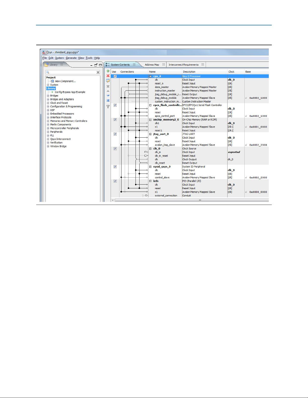
Figure 1–2 shows an example of a Qsys system containing the minimum component
set for a system with one CFI flash memory and an EPCS serial configuration device.
The system also includes other components which relate to the purpose of the system,
not to the flash programmer.
© March 2014 Altera Corporation Nios II Flash Programmer User Guide
Page 8
1–4 Chapter 1: Overview of the Nios II Flash Programmer
How the Flash Programmer Works
Figure 1–2. Example Target Design Containing the Minimum Component Set
1 Hardware example designs capable of programming the flash memory are provided
with Altera development boards. If you are developing for a custom board, consider
using one of these example designs as a starting point for your flash programmer
target design.
Nios II Flash Programmer User Guide © March 2014 Altera Corporation
Page 9

Introduction
2. Using the Flash Programmer GUI
The Nios II Flash Programmer GUI is an easy-to-use graphical interface that
automates the process of programming flash memory and enables you to control the
programming parameters easily. The Nios II Flash Programmer GUI lets you program
any combination of software, hardware, and binary data in flash memory in one
operation. The flash programmer GUI can also generate flash files for your future use,
and store them without programming the flash memory. Generating flash files or
programming flash memory from the flash programmer GUI generates a script for
future use from the command line.
You start the Nios II Flash Programmer GUI from the Nios II SBT for Eclipse or from
the command line.
Alternatively, you can use the flash programmer from the command line. Chapter 3,
Using the Flash Programmer from the Command Line describes the flash
programmer command-line utilities.
1 Altera recommends that you use the Nios II Flash Programmer GUI to generate
automated scripts, and use the scripts to automate the Nios II flash programming
process.
Starting the Flash Programmer GUI
To start the Nios II Flash Programmer GUI from the Nios II Command Shell, type the
following command:
nios2-flash-programmer-gui r
To start the Nios II Flash Programmer GUI from the Nios II SBT for Eclipse, on the
Nios II menu, click Flash Programmer.
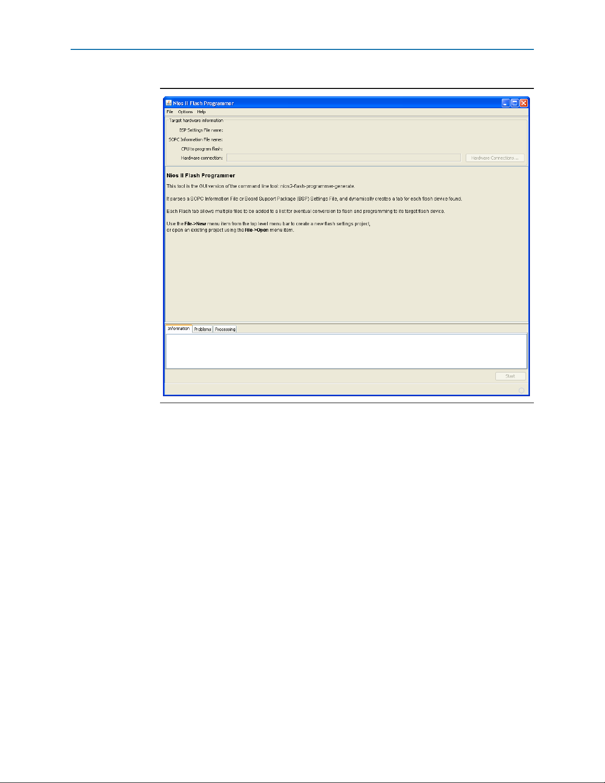
The Flash Programmer dialog box appears, as shown in Figure 2–1.
© March 2014 Altera Corporation Nios II Flash Programmer User Guide
Page 10
2–2 Chapter 2: Using the Flash Programmer GUI
Starting the Flash Programmer GUI
Figure 2–1. Flash Programmer Dialog Box
Specifying your Flash Programmer Settings
Before writing data to flash memory, you must determine the flash programmer
settings.
To create a new set of flash programmer settings, complete the following steps:
1. On the File menu, click New. The New Flash Programmer Settings File dialog
box appears.
2. Select Get flash programmer system details from BSP Settings File or Get flash
programmer system details from SOPC Information File.
3. Browse to locate your BSP Settings File (.bsp) or SOPC Information File
(.sopcinfo).
4. For a multiprocessor system, select the processor. If you specify a .bsp file, the
processor is already specified.
5. Click OK. The New Flash Programmer Settings File dialog box closes and the
Nios II Flash Programmer GUI populates with your processor selection, if
relevant, and the information from the .bsp or .sopcinfo file.
Nios II Flash Programmer User Guide © March 2014 Altera Corporation
Page 11
Chapter 2: Using the Flash Programmer GUI 2–3
Starting the Flash Programmer GUI
Depending on your selection in step 2, your flash programmer settings may not
include information about a BSP settings file. A new set of flash programmer settings
based on a BSP settings file includes the .sopcinfo file name, but a new set of flash
programmer settings based on a .sopcinfo file does not have information about a BSP
settings file to which it corresponds. In that case you must identify the .bsp file
explicitly. The .bsp file contains the information about your processor selection, for
example, whereas the .sopcinfo file knows about the available processors, but not
which one you selected.
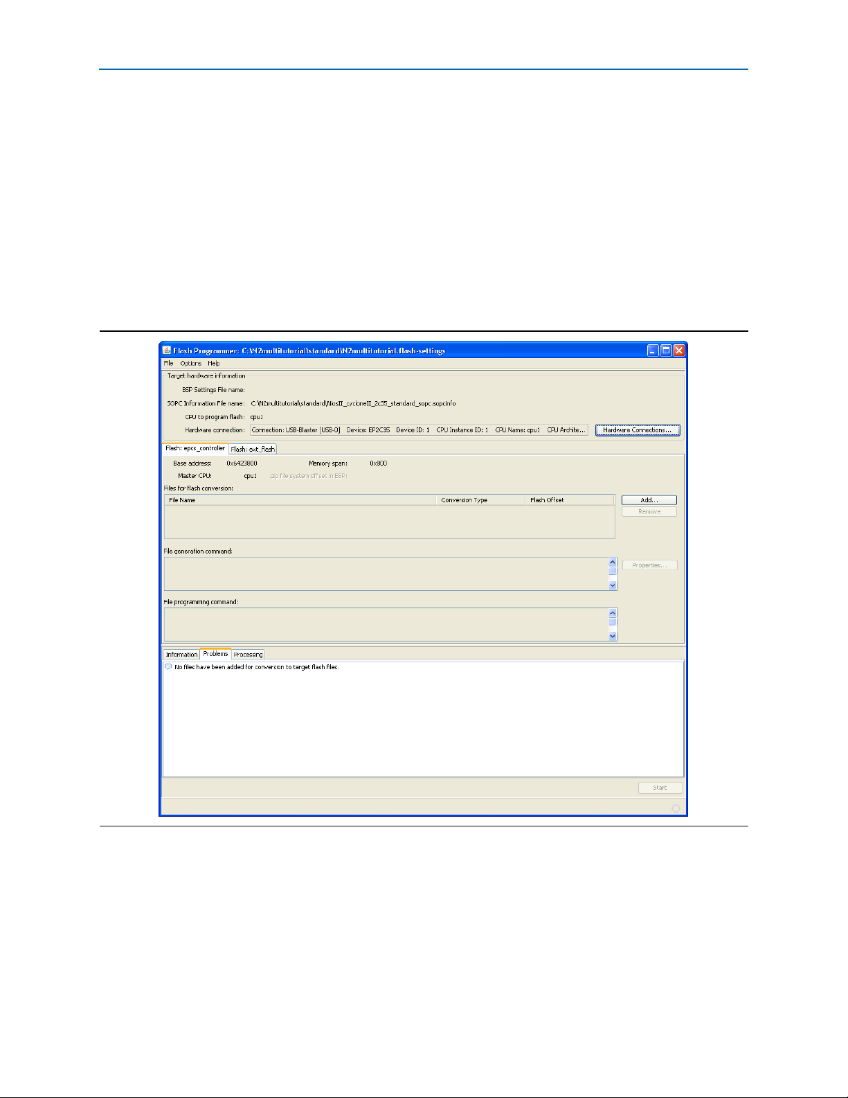
Figure 2–2 shows the flash programmer with a new set of flash programmer settings
based on the .sopcinfo file for a design with multiple processors and two flash
memory components.
Figure 2–2. Flash Programmer Dialog Box with Flash Programmer Settings
Working with Flash Programmer Settings Files
The Nios II Flash Programmer GUI is a powerful tool with many options. Altera
recommends saving your flash programmer settings in a Nios II Flash Programmer
Settings File (.flash-settings) for future use.
The .flash-settings file includes the settings described in the following sections, such
as the script and flash files directory paths, whether to perform system ID and system
timestamp checking, and whether to generate flash files or program flash memory.
© March 2014 Altera Corporation Nios II Flash Programmer User Guide
Page 12

2–4 Chapter 2: Using the Flash Programmer GUI
Starting the Flash Programmer GUI
To save your current flash programmer settings, on the File menu, click Save or Save
As to update or create a .flash-settings file. After you save the file, you can continue
to edit it in the Nios II Flash Programmer GUI.
To open a pre-existing flash programmer settings file, on the File menu, click Open,
and navigate to the location of the existing .flash-settings file.
Setting the Hardware Connection
This section describes how to select the correct download cable, device, and processor
to program flash memory. If your system has only a single download cable and a
single processor, the process is simple. This section describes all the steps for a system
with multiple download cables, processors, and devices.
Before you can program flash memory on your board, you must configure your FPGA
with a flash programmer target design that contains at least the minimum component
set specified in Table 1–1 on page 1–3.
f For instructions to configure the FPGA, refer to the Quartus II Programmer chapter in
volume 3 of the Quartus II Handbook.
After you load the target design on your FPGA, you can set the hardware connection
for programming flash memory.
To set the Hardware connection, perform the following steps:
1. Click Hardware Connections. The Hardware Connections dialog box appears.
2. In the Hardware Connections dialog box, click Refresh Connections.
3. If you are reusing an .flash-settings file, and the Quartus
recompiled since the .flash-settings file was created or the Name column entries
in the Processors list are blank, perform the following steps:
a. Under JTAG Debugging Information File name, browse to locate your project
JTAG Debugging Information File (.jdi).
b. Click Resolve Names. The flash programmer uses the .jdi file to ensure the
available connection information is accurate.
4. If your design has multiple download cables, select the appropriate cable.
5. If your design has multiple processors, select the Nios II processor that
corresponds to the CPU to program flash value under Target hardware
information in the Nios II Flash Programmer dialog box.
6. Click Close.
Checking System ID and System Timestamp
®
II project has been
If your flash programmer target design includes a System ID component, the Nios II
Flash Programmer can perform system ID and system timestamp checking before
programming flash memory. If the flash programmer performs system ID checking,
system timestamp checking, or both, and the expected system is not configured in the
FPGA, the flash programmer does not program the flash memory.
Nios II Flash Programmer User Guide © March 2014 Altera Corporation
Page 13

Chapter 2: Using the Flash Programmer GUI 2–5
Starting the Flash Programmer GUI
1 Altera recommends that your FPGA target design include a System ID component,
and that you enable both system ID and system timestamp checking.
By default, both system ID and system timestamp checking are enabled. To disable
checking for system ID or system timestamp, perform the following steps:
1. Click Hardware Connections. The Hardware Connections dialog box appears.
2. To disable system ID checking, turn on Ignore mismatched system ID.
3. To disable system timestamp checking, turn on Ignore mismatched system
timestamp.
4. Click Close.
After the hardware connections are set, you can confirm system ID and system
timestamp matching by performing the following steps:
1. Click Hardware Connections.
2. In the Hardware Connections dialog box, click System ID Properties.
3. Check that the Expected system ID and Actual system ID values match, and that
the Expected system timestamp and Actual system timestamp values match.
4. In the System ID Properties dialog box, click Close.
5. In the Hardware Connections dialog box, click Close.
For additional information about the system ID and system timestamp, refer to
Table 3–2 on page 3–2.
1 Regardless of the System ID component values, you cannot program flash memory if
the hardware design configured in the FPGA is not a valid flash programmer target
design that contains at least the minimum component set specified in Table 1–1 on
page 1–3.
Generating Flash Files and Programming Flash Memory
The Nios II Flash Programmer can generate flash files, program the flash memory
with a flash file, or both. The flash programmer can generate flash files from the
following different file types:
■ SRAM Object File (.sof) — Contains FPGA configuration data
■ Executable and Linking Format File (.elf)— Contains your executable application
software
■ Altera Zip Read-Only File System File (.zip) — Contains a read-only zip file
system associated with your Nios II software application project
■ An arbitrary binary file
f The Nios II EDS provides the Altera Zip Read-Only File System software component,
which is an easy-to-use tool for storing and accessing data in flash memory.
Depending on your application, you might find it more convenient to use the Zip
Read-Only File System, rather than storing raw binary data in flash memory. For
information about the Altera Zip Read-Only File System, refer to the Read-Only Zip
File System chapter in the Nios II Software Developer’s Handbook.
© March 2014 Altera Corporation Nios II Flash Programmer User Guide
Page 14

2–6 Chapter 2: Using the Flash Programmer GUI
Starting the Flash Programmer GUI
To generate flash files or to write to flash memory using your flash programmer
settings, perform the following steps:
1. On the Options menu, turn on the actions you wish to perform. The following
actions are available:
■ Generate Files—Generates flash files.
■ Program Files—Programs flash memory with the generated flash files.
■ Erase Flash Before Programming—Erases the entire flash memory before
writing each flash file to it.
■ Run From Reset After Programming—Runs the processor from its reset vector
after flash memory programming is complete.
The final two actions are relevant only if you turn on Program Files.
2. To specify the directories where you want the flash programmer to store the
generated flash files and script, on the Options menu, click Staging Directories
and specify the script and flash-files directory paths.
3. On the tab for the flash memory device you wish to target, under Files for flash
conversion, click Add.
The Nios II Flash Programmer adds the file to the Files for flash conversion list
and derives the flash offset from the file. Depending on your current Options
settings, the File generation command and File programming command boxes
populate with the command-line commands that generate the .flash file and
program it to your flash memory, respectively, providing a convenient way to
learn about the command-line utilities.
4. If you wish to pass any additional arguments to the file generation command,
under File generation command, click Properties.
5. If necessary, edit the Conversion Type settings for the files listed in the Files for
flash conversion table, by clicking the relevant table cells. Allowed conversion
types are ELF, SOF, and BINARY.
6. If necessary, edit the Flash Offset settings for the files listed in the Files for flash
conversion table, by double-clicking the relevant table cells.
1 Do not specify a flash offset for files of conversion type ELF.
7. Click Start. The Nios II Flash Programmer performs the actions specified by the
commands, storing the generated flash files to the specified flash directory, and
capturing the commands it runs to the flash_programmer.sh bash shell script in
the specified script directory.
1 You can use this script to duplicate the same actions again in the future, and
to learn about the command-line utilities.
Nios II Flash Programmer User Guide © March 2014 Altera Corporation
Page 15

3. Using the Flash Programmer from the Command Line
The Nios II development tools provide command-line utilities which give you
complete control of the Nios II Flash Programmer features. You can create a custom
script file to automate a flash programming task.
Alternatively, you can use the flash programmer GUI. Chapter 2, Using the Flash
Programmer GUI describes the flash programmer GUI.
1 The Nios II Flash Programmer GUI programs flash memory by creating a script based
on the command-line utilities. The script is well-formed, customized to your project,
and human-readable. You can use it as a reference for flash programmer
command-line syntax. The GUI-generated script is particularly helpful if you need to
use the --instance parameter listed in Table 3–2.
After you successfully program flash memory using the Nios II Flash Programmer
GUI, you can find the flash programmer script in the directory you specified in the
Staging Directories dialog box, available on the Options menu. The flash
programmer script is a file named flash_programmer.sh.
Table 3–1 lists the Nios II Flash Programmer command-line utilities.
Table 3–1. Flash Programmer Command-Line Utilities
nios2-flash-programmer Programs an S-record file into flash memory. Can also read back data,
verify data, provide debug information about the flash chip, and more.
sof2flash Converts an SRAM Object File (.sof) to an S-record file.
elf2flash Converts a Nios II Executable and Linking Format File (.elf) to an S-record
file.
bin2flash Converts an arbitrary data file to an S-record file.
The main utility for programming flash memory from the command line is
nios2-flash-programmer. It requires industry-standard S-record input files. These
utilities ensure that the input is compatible with the Nios II Flash Programmer. Input
file names for all utilities must include an explicit extension, such as .elf or .flash.
On Windows computers, when you launch the Nios II Command Shell, the flash
programmer utilities are available in your default search path.
f For more information about the Nios II Command Shell, refer to the Getting Started
from the Command Line chapter of the Nios II Software Developer's Handbook.
The following sections list the utilities and their functions.
© March 2014 Altera Corporation Nios II Flash Programmer User Guide
Page 16

3–2 Chapter 3: Using the Flash Programmer from the Command Line
nios2-flash-programmer
nios2-flash-programmer
The nios2-flash-programmer utility programs a preformatted file into a specified
flash memory. The input is an industry-standard S-record file, normally created by
one of the conversion utilities, sof2flash, elf2flash,orbin2flash.
nios2-flash-programmer can use any S-record file as an input, provided that the
addresses specified in the S-record file represent offsets from the beginning of flash
memory. The Nios II Flash Programmer GUI creates flash programmer files with a
.flash extension.
The nios2-flash-programmer utility is capable of programming, erasing, or reading
from any CFI-compatible flash memory or EPCS/EPCQ serial configuration device in
the hardware target design.
The nios2-flash-programmer command-line syntax is as follows:
nios2-flash-programmer [--help] [--cable=<cable name>]\
[--device=<device index>] [--instance=<instance>]\
[--sidp=<address>] [--id=<id>] [--timestamp=<time>]\
[--accept-bad-sysid] --base=<address> [--epcs]\
{ <file> } [--go]
1 Before you can program flash memory on your board, you must configure your FPGA
with a flash programmer target design that contains at least the minimum component
set specified in Table 1–1 on page 1–3.
f For instructions to configure the FPGA, refer to the Quartus II Programmer chapter in
volume 3 of the Quartus II Handbook.
Table 3–2 lists the parameters commonly used with nios2-flash-programmer.
Table 3–2. nios2-flash-programmer Parameters (Part 1 of 3)
Name Required Description
General Parameters
--cable=<cable name> Required if there are
multiple download
cables connected to the
host computer.
--device=<device index> Required if there are
multiple devices in the
JTAG chain.
--instance=<instance> Required if there are
multiple Nios II
processors with JTAG
debug modules in the
target design on the
FPGA.
--sidp=<address> Optional; required for
system ID validation.
Specifies which download cable to use.(1)
Specifies the FPGA's device number in the JTAG
chain. The device index specifies the device where
the flash programmer looks for the Nios II JTAG
debug module. JTAG devices are numbered relative
to the JTAG chain, starting at 1. (2)
Specifies which Nios II JTAG debug module to look
at in the FPGA. The instance ID specifies the JTAG
debug module that is used for programming flash
memory. (3)
Contains the base address of the System ID
component in your system. This value is in
hexadecimal format (for example, 0x01000000)
(4)
Nios II Flash Programmer User Guide © March 2014 Altera Corporation
Page 17

Chapter 3: Using the Flash Programmer from the Command Line 3–3
nios2-flash-programmer
Table 3–2.
nios2-flash-programmer Parameters (Part 2 of 3)
Name Required Description
--id=<id> Optional; required for
system ID validation.
Contains the ID value programmed into the System
ID component in your system. This value is
randomly selected each time you regenerate your
Qsys system. This value is in unsigned decimal
format (for example, 2056847728u) (5)
--timestamp=<time> Optional; required for
system timestamp
validation.
Contains the timestamp value programmed into the
System ID component in your system. Qsys sets this
value based on the time of system generation. This
value is in unsigned decimal format (for example,
1177105077u). Turning this parameter on is the
same as turning off the Ignore mismatched system
timestamp check box in the Nios II Flash
Programmer GUI Hardware Connections dialog
box.(6)
--accept-bad-sysid Optional; defaults off. Used to bypass the system ID validation. Forces the
flash programmer to download a flash image.
Turning this parameter on is the same as turning on
the Ignore mismatched system ID check box in the
Nios II Flash Programmer GUI Hardware
Connections dialog box.
--erase=<start>,<size> Optional; defaults off. Erases a range of bytes in the flash memory.
--erase-all Optional; defaults off. Erases the entire flash memory. The erase operation
occurs before programming, if an input file is
provided for programming.
--program Optional; defaults on if
Programs flash memory from the input files.
an input file is specified.
--no-keep-nearby Optional; defaults off Throws away partial sector data. If the data to
program does not completely fill the first or last
sector, the flash programmer normally preserves
and reprograms the original data in those sectors.
The --no-keep-nearby parameter disables this
feature. This option speeds up the programming
process, but is only appropriate if the existing flash
memory contents are unimportant.
--verify Optional; defaults off Verifies that contents of flash memory match input
files.
{ <file> } Optional Specifies the name(s) of the input file(s) to program
or verify. Separate multiple file names with spaces.
--read=<file> Optional; defaults off Reads flash memory contents into the specified file.
--read-bytes=<start>,<size> Optional if --read is
specified; defaults off
Specifies which address range to read (byte
addresses).
--go Optional; defaults off Runs the processor from its reset vector after flash
memory programming is complete.
CFI Parameters
--debug Optional; defaults off Prints debug information, including the flash
memory's query table.
© March 2014 Altera Corporation Nios II Flash Programmer User Guide
Page 18

3–4 Chapter 3: Using the Flash Programmer from the Command Line
nios2-flash-programmer
Table 3–2. nios2-flash-programmer Parameters (Part 3 of 3)
Name Required Description
--base=<address> Required Specifies the base address of the CFI flash memory.
This parameter is the absolute address in the target
design's address space. nios2-flash-programmer
treats addresses in the S-record files as offsets to
the base address.
EPCS Parameters
--epcs Required when
programming an
Specifies that the target flash memory is an
EPCS/EPCQ serial configuration device.
EPCS/EPCQ serial
configuration device;
defaults off
--debug Optional; defaults off Prints debug information about the physical memory
inside the EPCS/EPCQ device.
--base=<address> Required Specifies the base address of the EPCS/EPCQ device.
Notes to Table 3–2:
(1) The --cable parameter is only needed if there are multiple download cables connected to the host computer. To determine the cable names,
run jtagconfig.
(2) The --device parameter is only needed if there are two or more processors in different devices with the same instance ID. To determine the
JTAG device index, run jtagconfig.
(3) There are two ways to find the correct value of the instance ID for a processor. The easiest is to use the Nios II Flash Programmer GUI to create
a sample flash programmer script. Refer to Chapter 2, Using the Flash Programmer GUI for details. Alternatively, open <Quartus II project
name>.jdi, in the Quartus II project directory. Locate the Nios II processor node by finding a value of hpath containing <processor module
name>=. The instance ID is specified as instance_id.
(4) In system.h and in your board support package (BSP), the system ID base address is specified by SYSID_BASE.
(5) In system.h and in your BSP the system ID value is specified by SYSID_ID.
(6) In system.h and in your BSP, the system ID time stamp is specified by SYSID_TIMESTAMP.
f For additional parameters, type nios2-flash-programmer --help at a
command line.
nios2-flash-programmer Command-Line Examples
nios2-flash-programmer --cable="Usb-blaster [USB-0]" --base=0x200000\
--program ext_flash.flash
Programs CFI flash memory based at address 0x200000 with input file ext_flash.flash
using a cable named "Usb-blaster [USB-0]"
nios2-flash-programmer --epcs --base=0x02100000 epcs_controller.flash
Programs an EPCS/EPCQ device based at address 0x02100000 with input file
epcs_controller.flash.
nios2-flash-programmer --base=0x200000 --read=current.srec \
--read-bytes=0,0x10000
Reads 0x10000 bytes from CFI flash memory based at address 0x200000 and writes the
contents to a file named current.srec
nios2-flash-programmer --base=0x200000 --erase=0x8000,0x10000
Erases address range 0x8000 to 0x10000 in CFI flash memory based at address
0x200000
nios2-flash-programmer --base=0x200000 --debug
Nios II Flash Programmer User Guide © March 2014 Altera Corporation
Page 19

Chapter 3: Using the Flash Programmer from the Command Line 3–5
sof2flash
Queries CFI flash memory based at address 0x200000 and reports the result. This
command dumps the flash memory's query table.
sof2flash
The sof2flash utility takes an SRAM Object File and translates it to an S-record file,
suitable for programming into flash memory.
Table 3–3 lists the typical parameters used with sof2flash.
Table 3–3. sof2flash Parameters
Name Required Description
General Parameters
--compress Optional Turns on compression. Available for Cyclone
Cyclone III, Stratix
®
II, and Stratix III devices.
--input=<file> Required Name of the input SRAM Object File.
--output=<file> Required Name of the output file.
CFI Parameters
--offset=<addr> Required Offset within the flash memory device where the FPGA
configuration is to be programmed.
®
II,
EPCS Parameters
--epcs Required for EPCS
Specifies that the output is intended for an EPCS device.
devices; defaults off
--epcq (2) Required for EPCQ
Specifies that the output is intended for an EPCQ device.
devices
Device Specific Parameters
--activeparallel Optional Creates parallel flash contents compatible with
active-parallel configuration mode. Only available on
FPGAs which support active-parallel configuration.
--pfl (1) Required if your
FPGA configuration
uses the PFL
--optionbit=<optionbitaddr>
(1)
Required if your
FPGA configuration
uses the PFL
Specifies that the flash programmer use the parallel flash
loader. Required if your FPGA configuration uses the
parallel flash loader (PFL).
Specifies the option bit address in your flash memory
device. When you use this option, the sof2flash
command generates both a .flash file and a .map.flash
file. When you program the flash memory with the
.map.flash file, it overwrites the default option bits. In
almost all cases, the default option bits are appropriate
and you should not program this file to flash.
Note to Table 3–3:
(1) Using the --pfl and --optionbits command-line options slows down sof2flash generation noticeably. For more information about
when to use the --pfl and --optionbits command-line options, refer to AN386: Using the Parallel Flash Loader with the Quartus II
Software.
(2) From Nios II EDS 13.1 onwards, the -epcq option is required for V-series devices and above to program an EPCQ device.
f For additional parameters, type sof2flash --help at a command line.
© March 2014 Altera Corporation Nios II Flash Programmer User Guide
Page 20

3–6 Chapter 3: Using the Flash Programmer from the Command Line
elf2flash
sof2flash Command-Line Examples
sof2flash --offset=0x0 --input=standard.sof \
--output=standard_cfi.flash
Converts standard.sof to an S-record file named standard_cfi.flash intended for a CFI
flash memory. The S-record offset begins at 0x0.
sof2flash --epcs --input=standard.sof --output=standard_epcs.flash
Converts standard.sof to an S-record file named standard_epcs.flash intended for an
EPCS device.
sof2flash --epcq --input=standard.sof --output=standard_epcq.flash
Converts standard.sof to an S-record file named standard_epcq.flash intended for an
EPCQ device.
sof2flash --optionbit=0x18000 --pfl --input=standard.sof \
--output=standard.flash --offset=0x640000
Converts standard.sof to an S-record file named standard.flash for use with the
parallel flash loader, and generates an option-bits overwrite file standard.map.flash
for option bits at offset 0x18000 on the flash memory device.
elf2flash
1 Altera recommends that you not use the standard.map.flash file even if you generate
it. The --optionbit command-line option is required for correct functioning of the
--pfl option, but the resulting overwrite file should be ignored.
The elf2flash utility takes an Executable and Linking Format File, and translates it to
an S-record file suitable for programming into flash memory.
elf2flash also inserts a boot copier into the flash file, if needed. elf2flash inserts the
boot copier code before the application code under the following conditions:
■ The processor’s reset address falls within the address range of the flash memory
being programmed.
■ The executable code is linked to a memory location outside of the flash memory
being programmed.
If elf2flash inserts a boot copier, it also translates the application executable and
linking format file to a boot record for use by the boot copier. This boot record
contains all of the application code, but is not executable. After reset, the boot copier
reads the boot record from flash memory and copies the application code to the
correct linked address, and then branches to the newly-copied application code.
Table 3–4 lists the typical parameters used with elf2flash.
Table 3–4. elf2flash Parameters (Part 1 of 2)
Name Required Description
General Parameters
--input=<file> Required. The name of the input Executable and Linking Format File.
--output=<file> Required. The name of the output file.
Nios II Flash Programmer User Guide © March 2014 Altera Corporation
Page 21

Chapter 3: Using the Flash Programmer from the Command Line 3–7
elf2flash
Table 3–4. elf2flash Parameters (Part 2 of 2)
Name Required Description
CFI Parameters
--base=<addr> Required. The base address of the flash memory component. elf2flash uses this
parameter with --end and --reset to determine whether the system
requires a boot copier.
--end=<addr> Required. The end address of the flash memory component. elf2flash uses this
parameter with --base and --reset to determine whether the system
requires a boot copier.
--reset=<addr> Required. The processor reset address, which is specified in Qsys. elf2flash uses
this parameter with --base and --end to determine whether the
system requires a boot copier.
--boot=<file> Required under the
following conditions:
■ The processor's
reset address falls
within theaddress
Specifies the boot copier object code file. Ignored if the boot copier is not
required. If elf2flash determines that a boot copier is required, but the
--boot parameter is absent, elf2flash displays an error message. The
Altera-provided boot copier resides at <Nios II EDS install
path>/components/altera_nios2/boot_loader_cfi.srec.
range of the flash
memory being
programmed.
■ The executable
code is linked to a
memory location
outside of the
flash memory
being
programmed.
EPCS Parameters
--epcs Required when
Specifies that the output is intended for an EPCS/EPCQ device.
creating files for an
EPCS/EPCQ device;
defaults off.
--after=<file> Required when
programming both
hardware and
software into an
elf2flash uses this parameter to position a Nios II executable in an
EPCS/EPCQ device along with an FPGA configuration. For further details,
see “Programming Both Hardware and Software into an EPCS/EPCQ
Device”.
EPCS/EPCQ device
f For additional parameters, type elf2flash --help at a command line.
Programming Both Hardware and Software into an EPCS/EPCQ Device
The --base parameter is not available for EPCS/EPCQ devices, because in
EPCS/EPCQ devices, FPGA configuration data must start at address 0x0. However, if
you are programming both an FPGA configuration and a Nios II software executable
in the EPCS/EPCQ device, the --after parameter lets you position the software
executable directly after the FPGA configuration data.
© March 2014 Altera Corporation Nios II Flash Programmer User Guide
Page 22

3–8 Chapter 3: Using the Flash Programmer from the Command Line
bin2flash
Convert the FPGA configuration file first using sof2flash. When converting the
Nios II software executable, use the --after parameter, and specify the FPGA
configuration S-record file. The S-record output for the software executable starts at
the first address unused by the FPGA configuration. Refer to the second example
under “elf2flash Command-Line Examples”.
1 elf2flash does not insert the FPGA configuration into the output file. It simply leaves
space, starting at offset 0x0, that is large enough for the configuration data.
1 In Quartus II software version 13.1 and onwards, the -epcs/--epcq option in
sof2flash generates .flash file with a SOF header, which contains the SOF length. This
change is required for V-series devices and above for new SOF format, and to allow
for future SOF format variations. The Nios II bootcopier loads the Nios II software
executable from EPCS/EPCQ devices based on the SOF length. Please refer to KDB
Solution rd11192013_118 for how to program EPCS/EPCQ devices.
elf2flash Command-Line Examples
elf2flash --base=0x0 --reset=0x0 --boot=boot_loader_cfi.srec \
--input=myapp.elf --output=myapp.flash
Converts myapp.elf to an S-record file named myapp.flash, intended for a CFI flash
memory based at 0x0. Includes a boot copier (from boot_loader_cfi.srec), which is
required in this example because --base and --reset are equal.
elf2flash --epcs --after=standard.flash --input=myapp.elf \
--output=myapp.flash
Converts myapp.elf to an S-record file named myapp.flash, intended for an EPCS
device. The S-record output starts at the first address unused by standard.flash.
bin2flash
The bin2flash utility converts an arbitrary file to an S-record file suitable for use by
the flash programmer. You can use bin2flash to convert read-only binary data needed
by a Nios II program, such as software configuration tables.
Depending on your application, you might find it more convenient to use the Altera
Read-Only Zip Filing System, which serves the same purpose.
f For information about the Altera Zip Read-Only File System, refer to the Read-Only
Zip File System chapter in the Nios II Software Developer’s Handbook.
Do not use bin2flash to convert executable software files or FPGA configuration files.
To convert Nios II software executable files, use elf2flash. To convert FPGA
configuration files, use sof2flash.
Table 3–5 lists the typical parameters used with bin2flash.
Table 3–5. bin2flash Parameters (Part 1 of 2)
Name Required? Default Description
--location=<addr> Required — Offset within the flash memory where the data is to be
programmed
Nios II Flash Programmer User Guide © March 2014 Altera Corporation
Page 23

Chapter 3: Using the Flash Programmer from the Command Line 3–9
bin2flash
Table 3–5. bin2flash Parameters (Part 2 of 2)
Name Required? Default Description
--input=<file> Required — Name of the input binary file being converted
--output=<file> Required — Name of the output file
f For additional parameters, type elf2flash --help at a command line.
bin2flash Command-Line Example
bin2flash --location=0x40000 --input=data.bin --output=data.flash
Converts data.bin to an S-record file named data.flash. Addresses in the S-record file
place the data starting at offset 0x40000 from the beginning of flash memory.
© March 2014 Altera Corporation Nios II Flash Programmer User Guide
Page 24

3–10 Chapter 3: Using the Flash Programmer from the Command Line
bin2flash
Nios II Flash Programmer User Guide © March 2014 Altera Corporation
Page 25

This section covers advanced topics to support non-standard CFI flash memory. To
use the procedures in this section, you need the data sheet for the flash memory
device you are using. Make sure you fully understand the CFI aspects of the device.
Some CFI flash memory devices contain missing or incorrect CFI table information. In
such cases, the Nios II Flash Programmer might fail based on the erroneous
information in the CFI table. For these devices, the Nios II Flash Programmer
provides the following methods to override the CFI table and successfully program
flash memory:
■ Built-in recognition and override
■ Flash override files
■ Width mode override
Built-in Recognition and Override
A. Non-Standard Flash Memories
The Nios II Flash Programmer contains code to recognize some devices with known
CFI table problems. On these devices, it overrides the incorrect table entries. Always
try using built-in recognition and override before trying to create an override file. To
determine whether the flash programmer recognizes the device, run the flash
programmer from the command line with the --debug option. If the flash
programmer overrides the CFI table, the flash programmer displays a message
"Override data for this device is built in".
f For details on using the flash programmer from the command line, refer to Chapter 3,
Using the Flash Programmer from the Command Line.
Flash Override Files
To support newly released flash memory devices which might have problems in the
CFI table, the Nios II Flash Programmer provides the ability to override CFI table
entries with flash override files. A flash override file lets you manually override
erroneous information in the CFI table, which enables the Nios II Flash Programmer
to function correctly.
Before creating an override file, run nios2-flash-programmer from the command line
with the --debug parameter, which lists the CFI table found in the device. Compare
the debug output with the device's data sheet.
Flash Override File Format
Flash override files contain two sections for each flash memory they override. The
first section declares the flash memory type. The second section is the CFI table
override data. The flash override file can contain comments preceded by a '#'
character.
© March 2014 Altera Corporation Nios II Flash Programmer User Guide
Page 26

A–2 Appendix A: Non-Standard Flash Memories
Width Mode Override Parameter
For example, the SST 39VF800 flash memory contains three incorrect entries in its CFI
table at location 0x13, 0x14, and 0x2C. The following example demonstrates how to
override the values at those addresses.
[FLASH-00BF-2781] # Keyword FLASH, followed by the Mfgr ID and Device ID
CFI[0x13] = 0x02 # The primary command set, found at CFI table CFI[0x14] = 0x00 # addresses 0x13 and 0x14 are overridden to
CFI[0x2C] = 0x01 # The number of CFI Erase block regions, found at
1 This example is for illustration only. nios2-flash-programmer recognizes the SST
39VF800 as a nonstandard CFI device and overrides its CFI table. You do not need to
create an override file for this particular part.
How to Use the Flash Override File
There are two ways to deploy flash override files:
1. Place the override file in <Nios II EDS install path>/bin. The Nios II Flash
Programmer searches this directory for all filenames matching the pattern nios2-
flash-override*. The flash programmer loads all these files as override files.
2. Pass the override file to the flash programmer with the --override parameter.
The following example illustrates this parameter:
nios2-flash-programmer --base 0x0 -–override=my_override.txt sw.flash
# These ID values can be found in three ways:
# -by consulting the flash memory device's data sheet.
# -by using the "autoselect" command
# -by running nios2-flash-programmer --debug
# 0x02, 0x00.
# CFI table –address 0x2C is overridden to 0x1.
Width Mode Override Parameter
The override procedure described in “Flash Override Files” assumes the Nios II Flash
Programmer detects the correct data-width mode from the CFI query table. In some
cases, a 16-bit CFI flash memory device wired in 8-bit mode might return a query
table indicating 16-bit mode. This condition prevents the flash programmer from
correctly interpreting the remainder of the query table. The flash programmer cannot
detect this situation, because the device type is unreadable. If your flash memory
device has this problem, you must program it from the command line.
In this case, override the data width on the command line with the hidden parameter
--width=8.
This parameter is known to be necessary for only two flash memory devices: the ST
Micro ST29W800 and ST29W640. Unless you are using these devices, you are unlikely
to require this parameter.
Nios II Flash Programmer User Guide © March 2014 Altera Corporation
Page 27

B. Supported Flash Memory Devices
The Nios II Flash Programmer works with all CFI-compatible parallel flash memories
that support programming algorithm 1, 2, or 3, and with all Altera EPCS/EPCQ serial
configuration devices. Not all flash memory devices have been tested with the Nios II
Flash Programmer.
1 If you find a CFI-compliant device that does not work with the Nios II Flash
Programmer, please report it to Altera Technical Support.
© March 2014 Altera Corporation Nios II Flash Programmer User Guide
Page 28

B–2 Appendix B: Supported Flash Memory Devices
Nios II Flash Programmer User Guide © March 2014 Altera Corporation
Page 29

C. Stand-Alone Mode
While developing hardware or software, you use the Nios II Flash Programmer on a
computer with the Quartus II software and the Nios II EDS installed. However, in a
production or service environment you might want to set up a computer to program
flash memory without installing the full set of Altera development tools. A
stand-alone version of the Nios II Flash Programmer is available for this purpose.
In stand-alone mode, the flash programmer has limited functionality. You can
program any type of CFI or EPCS flash memory. However, the elf2flash, sof2flash,
and bin2flash utilities are not available. You must create input files for the flash
programmer on a computer which has the Nios II development tools fully installed.
Installing the Nios II Stand-Alone Flash Programmer
To install the Nios II Flash Programmer in stand-alone mode, perform the following
steps:
1. Install the Quartus II Stand-Alone Programmer from the Quartus II CD. The
nios2-flash-programmer utility requires the Quartus II Stand-Alone Programmer
to access the JTAG chain on the board.
2. On a computer which has the Nios II EDS fully installed, find the executable file
<Nios II EDS install path>/bin/nios2-flash-programmer.exe.
3. On the stand-alone computer, copy nios2-flash-programmer.exe to the directory
<Quartus II Stand-Alone Programmer Path>/bin.
4. On the computer with the full Nios II EDS installation, find the Windows library
file c:/cygwin/bin/cygwin1.dll. If you install cygwin separately from the Nios II
EDS, your cygwin DLLs might reside in a different directory.
5. On the stand-alone computer, copy cygwin1.dll into c:/cygwin/bin (or the
equivalent path, based on the cygwin installation).
Running the Nios II Stand-Alone Flash Programmer
To run the Nios II Flash Programmer in stand-alone mode, perform the following
steps:
1. Open a command prompt on the stand-alone computer. Change directories to the
location of the files you wish to program into flash memory.
2. Run the nios2-flash-programmer utility as described in Chapter 3, Using the Flash
Programmer from the Command Line.
© March 2014 Altera Corporation Nios II Flash Programmer User Guide
Page 30

C–2 Appendix C: Stand-Alone Mode
Running the Nios II Stand-Alone Flash Programmer
Nios II Flash Programmer User Guide © March 2014 Altera Corporation
Page 31

D. Troubleshooting
Overview
This chapter lists troubleshooting tips for the Nios II Flash Programmer. Each section
in this chapter describes a common issue you might run into when using the Nios II
Flash Programmer.
Start Button Grayed Out in the Flash Programmer GUI
In the Nios II Flash Programmer GUI, even after a flash programmer configuration is
opened, the Start button appears grayed out.
Probable Cause
You have not fully specified the required parameters for programming flash memory.
Suggested Actions
■ Check the Problems tab for any information about what may be missing or
incorrect.
■ Make sure that your JTAG cable settings are correct. Specify the connection in the
Hardware Connections dialog box, by clicking Refresh Connections and Resolve
Names, and selecting the Nios II processor that matches the value in CPU to
program flash.
■ Make sure that you have selected a file to program to the flash memory, and that it
appears with the correct Conversion Type and Flash Offset values.
"No Nios II processors available" Error
When you run the flash programmer, you get the error: "There are no Nios II
processors available which match the values specified. Please check that your PLD is
correctly configured, downloading a new .sof file if necessary."
Probable Cause
The flash programmer is unable to connect with a Nios II JTAG debug module inside
the FPGA.
Suggested Actions
■ Make sure that the FPGA is running a valid flash programmer target design. If not,
you need to configure the FPGA using the Quartus II programmer. Refer to “Flash
Programmer Target Design” on page 1–3.
■ If using the flash programmer from the command line, ensure you have specified
the proper --device, --cable, and --instance parameter values. Refer to
Chapter 3, Using the Flash Programmer from the Command Line for details.
© March 2014 Altera Corporation Nios II Flash Programmer User Guide
Page 32

D–2 Appendix D: Troubleshooting
"No CFI table found" Error
"No CFI table found" Error
When you run the flash programmer to program CFI flash memory, you get the error:
"No CFI table found at address <base address>"
Probable Cause
The flash programmer can connect with a Nios II JTAG debug module in the FPGA,
but it can not successfully execute a query to a flash memory at the base address
specified.
Suggested Actions
■ If you are using nios2-flash-programmer from the command line, make sure you
specified the correct base address for the CFI device. You can find the flash
memory's base address in Qsys.
■ Run nios2-flash-programmer from the command line with the --debug
parameter. This command dumps the flash memory's query table. Compare the
output with the flash memory device's data sheet. For further details, see
Chapter 3, Using the Flash Programmer from the Command Line.
■ Ensure your flash memory hardware is correctly connected to place it at the base
address specified in Qsys. Verify the base address by running the "Test Flash"
routine in the "Memory Test" software template provided in the Nios II EDS. If the
test fails, there is a problem with your memory connection. There are two places to
look for the problem:
■ The physical connection on your target board
■ The pin assignments on the top-level FPGA design
■ If all else fails, make sure the flash memory device you are using does not require
an override file. Refer to Appendix A, Non-Standard Flash Memories for details.
"No EPCS registers found" Error
When you run the flash programmer to program an EPCS device, you get the error:
"No EPCS registers found: tried looking at addresses...."
Probable Cause
The flash programmer can connect with a Nios II JTAG debug module in the FPGA,
but it can not successfully find an EPCS device located at the specified base address.
Suggested Actions
■ Reconfigure the FPGA with a valid target design via JTAG using the Quartus II
programmer. If the FPGA is configured by another method, such as by a
configuration controller, the pins that connect to the EPCS device might be
disabled.
■ If you are using nios2-flash-programmer from the command line, make sure you
specified the correct base address for your EPCS device. You can find the flash
memory's base address in Qsys.
Nios II Flash Programmer User Guide © March 2014 Altera Corporation
Page 33

Appendix D: Troubleshooting D–3
"System does not have any flash memory" Error
■ Ensure that the EPCS device is correctly connected to the FPGA on the board.
Verify the EPCS connection by running the "Test EPCS" routine in the "Memory
Test" software template provided by the Nios II EDS. If the test fails, there is a
problem with your memory connection. There are two places to look for the
problem:
■ The physical connection on your target board
■ The pin assignments on the top-level FPGA design
■ Use the Quartus II Programmer to program the EPCS device directly via a JTAG
download cable, and verify that the EPCS device successfully configures the
FPGA.
■ Run nios2-flash-programmer from the command line with the --epcs parameter.
This command displays information about the flash memory in the EPCS device.
For further details, see Chapter 3, Using the Flash Programmer from the
Command Line.
"System does not have any flash memory" Error
When you run the flash programmer, you get the error: "The Qsys system does not
have any flash memory."
Probable Cause
The FPGA is not currently configured with a valid flash programmer target design.
Suggested Actions
If practical, upgrade your FPGA design to meet the criteria for a flash programmer
target design. Refer to “Flash Programmer Target Design” on page 1–3 for details.
"Reading System ID at address 0x<address>: FAIL" Error
When you run the Nios II Flash Programmer GUI, you get the error: "Reading System
ID at address 0x<address>: FAIL"
Probable Cause
The FPGA is not currently configured with the target design that corresponds to the
BSP project for the software application in the Nios II Software Build Tools for Eclipse.
Suggested Actions
Use the Quartus II Programmer to download the correct FPGA configuration file to
the FPGA, then try using the Nios II Flash Programmer again.
"Base address not aligned on size of device" Error
When you run the flash programmer, you get the error message Base address not
aligned on size of device.
© March 2014 Altera Corporation Nios II Flash Programmer User Guide
Page 34

D–4 Appendix D: Troubleshooting
"Base address not aligned on size of device" Error
Probable Cause
The flash device base address being passed to the Flash Programmer is not a multiple
of the flash device's size.
Suggested Actions
■ Ensure that the flash device is mapped to a base address in Qsys that is a multiple
of the flash size listed in its CFI table.
■ If in command line mode, ensure that the --base parameter you are passing to
nios2-flash-programmer is the correct base address of the flash device in your
Qsys system.
Nios II Flash Programmer User Guide © March 2014 Altera Corporation
Page 35

Additional Information
Revision History
The following table shows the revision history for this user guide.
Date Version Changes Made
March 2014 2.2
February 2010 2.1
January 2010 2.0
May 2008 1.6 In chapter 3, corrected error in Table 3–3 on page 3–5. The default mode for the compression
November 2007 1.5
May 2007 1.4
November 2006 1.3 Updates for the Nios II version 6.1 release. Includes improvements to the flash programmer
October 2005 1.2 Updates for the Nios II version 5.1 release. Includes major changes to the flash programmer
December 2004 1.1 Updates for the Nios II version 1.1 release.
May 2004 1.0 Initial release.
■ In chapter 1, added cross-reference to the Quad-Serial Configuration (EPCQ) Devices
Datasheet
■ In chapter 1, updated Table 1–1 and updated the table notes.
■ In chapter 1, updated Figure 1–2.
■ In chapter 3, updated Table 3–3.
■ In chapter 3, added the EPCQ command line example.
■ In chapter 3, updated Table 3–4.
■ In chapter 3, added a note about how to program EPCS/EPCQ devices.
■ Replaced SOPC Builder with Qsys.
■ Replaced “EPCS” with “EPCS/EPCQ.”
■ Documented the two sof2flash options --pfl and --optionbit.
■ Documented the new Nios II Flash Programmer GUI.
■ Revised entire document to use Nios II Software Build Tools for Eclipse instead of
Nios II IDE.
■ Removed out-of-date list of tested flash memory devices.
parameter is on. Compression is available for Cyclone II, Cyclone III, Stratix II, and Stratix III
devices.
■ In chapter 1, added note that Hardcopy II devices also support programming CFI Flash
using Nios II Flash programmer.
■ In chapter 3, documented command-line support for active parallel configuration.
■ In chapter 1, removed mention of board description files (no longer implemented)
■ In chapter 1, corrected and updated discussion of --instance and --device
command line parameters
■ In chapter 1, updated SOPC Builder screen shot
■ In chapter 3, added descriptions of nios2-flash-programmer options --sidp, --id,
--timestamp, --accept-bad-sysid
■ In appendix C, corrected missing installation step
■ In appendix C, removed mention of board description files (no longer implemented)
user interface.
target design.
© March 2014 Altera Corporation Nios II Flash Programmer User Guide
Page 36

Info–2 Additional Information
How to Contact Altera
How to Contact Altera
For the most up-to-date information about Altera®products, see the following table.
Contact
Contact (Note 1)
Method Address
Technical support Website www.altera.com/support
Technical training Website www.altera.com/training
Email custrain@altera.com
Technical documentation Website www.altera.com/literature
Continued...
Non-technical support (General)
(Software Licensing)
Note:
(1) You can also contact your local Altera sales office or sales representative.
Email nacomp@altera.com
Email authorization@altera.com
Typographic Conventions
The following table shows the typographic conventions that this document uses.
Visual Cue Meaning
Bold Type with Initial Capital Letters
Command names, dialog box titles, check box options, and dialog box options are
shown in bold, initial capital letters. Example: Save As dialog box.
bold type External timing parameters, directory names, project names, disk drive names, file
names, file name extensions, and software utility names are shown in bold type.
Examples: f
, \qdesigns directory, d: drive, chiptrip.gdf file.
MAX
Italic Type with Initial Capital Letters Document titles are shown in italic type with initial capital letters. Example: AN 75:
High-Speed Board Design.
Italic type Internal timing parameters and variables are shown in italic type.
Examples: t
PIA
, n +1.
Variable names are enclosed in angle brackets (< >) and shown in italic type.
Example: <file name>, <project name>.pof file.
Initial Capital Letters Keyboard keys and menu names are shown with initial capital letters. Examples:
Delete key, the Options menu.
“Subheading Title” References to sections within a document and titles of on-line help topics are shown
in quotation marks. Example: “Typographic Conventions.”
Courier type Signal and port names are shown in lowercase Courier type. Examples: data1, tdi,
input. Active-low signals are denoted by suffix n, e.g., resetn.
Anything that must be typed exactly as it appears is shown in Courier type. For example:
c:\qdesigns\tutorial\chiptrip.gdf. Also, sections of an actual file,
such as a Report File, references to parts of files (e.g., the AHDL keyword
SIGN
), as well as logic function names (e.g., TRI) are shown in Courier.
1., 2., 3., and
a., b., c., etc.
■ ■ Bullets are used in a list of items when the sequence of the items is not important.
Numbered steps are used in a list of items when the sequence of the items is important, such as the steps listed in a procedure.
SUBDE-
v The checkmark indicates a procedure that consists of one step only.
1 The hand points to information that requires special attention.
Nios II Flash Programmer User Guide © March 2014 Altera Corporation
Page 37

Additional Information Info–3
Typographic Conventions
Visual Cue Meaning
c
w
A caution calls attention to a condition or possible situation that can damage or
destroy the product or the user’s work.
A warning calls attention to a condition or possible situation that can cause injury to
the user.
r The angled arrow indicates you should press the Enter key.
f The feet direct you to more information about a particular topic.
© March 2014 Altera Corporation Nios II Flash Programmer User Guide
 Loading...