

Page 1

NCO IP Core
User Guide
Subscribe
Send Feedback
UG-NCO
2014.12.15
101 Innovation Drive
San Jose, CA 95134
www.altera.com
Page 2

TOC-2
Contents
About the NCO IP Core...................................................................................... 1-1
NCO IP Core Getting Started............................................................................. 2-1
Altera DSP IP Core Features...................................................................................................................... 1-1
NCO IP Core Features................................................................................................................................ 1-2
DSP IP Core Device Family Support.........................................................................................................1-2
NCO IP Core MegaCore Verification.......................................................................................................1-3
NCO IP Core Release Information............................................................................................................1-3
NCO IP Core Performance and Resource Utilization............................................................................1-4
Installing and Licensing IP Cores..............................................................................................................2-1
OpenCore Plus IP Evaluation........................................................................................................ 2-1
NCO IP Core OpenCore Plus Timeout Behavior....................................................................... 2-2
IP Catalog and Parameter Editor...............................................................................................................2-2
Specifying IP Core Parameters and Options............................................................................................2-3
Files Generated for Altera IP Cores...............................................................................................2-5
Simulating Altera IP Cores in other EDA Tools..................................................................................... 2-8
DSP Builder Design Flow............................................................................................................................2-9
NCO IP Core Functional Description................................................................ 3-1
NCO IP Core Architectures....................................................................................................................... 3-2
Large ROM Architecture................................................................................................................ 3-2
Small ROM Architecture................................................................................................................ 3-2
CORDIC Architecture.....................................................................................................................3-3
Multiplier-Based Architecture....................................................................................................... 3-4
Multichannel NCOs.....................................................................................................................................3-5
Frequency Hopping.....................................................................................................................................3-5
Phase Dithering............................................................................................................................................3-6
Frequency Modulation................................................................................................................................3-7
Phase Modulation........................................................................................................................................3-7
NCO IP Core Parameters........................................................................................................................... 3-7
Architecture Parameters................................................................................................................. 3-7
Frequency Parameters.....................................................................................................................3-8
Optional Ports Parameters..............................................................................................................3-9
NCO IP Core Interfaces and Signals.........................................................................................................3-9
Avalon-ST Interfaces in DSP IP Cores..........................................................................................3-9
NCO IP Core Signals.....................................................................................................................3-10
NCO IP Core Timing Diagrams..................................................................................................3-11
NCO Multichannel Design Example...................................................................4-1
NCO Design Example Specification..........................................................................................................4-2
Altera Corporation
Page 3

TOC-3
Opening the NCO Multichannel Design Example..................................................................................4-4
Document Revision History................................................................................5-1
Altera Corporation
Page 4
2014.12.15
Constellation
Mapper
IF Signal
NCO
Q
I
FIR
Filter
FIR
Filter
cos(wt)
sin(wt)
www.altera.com
101 Innovation Drive, San Jose, CA 95134
About the NCO IP Core
1
UG-NCO
Subscribe
Send Feedback
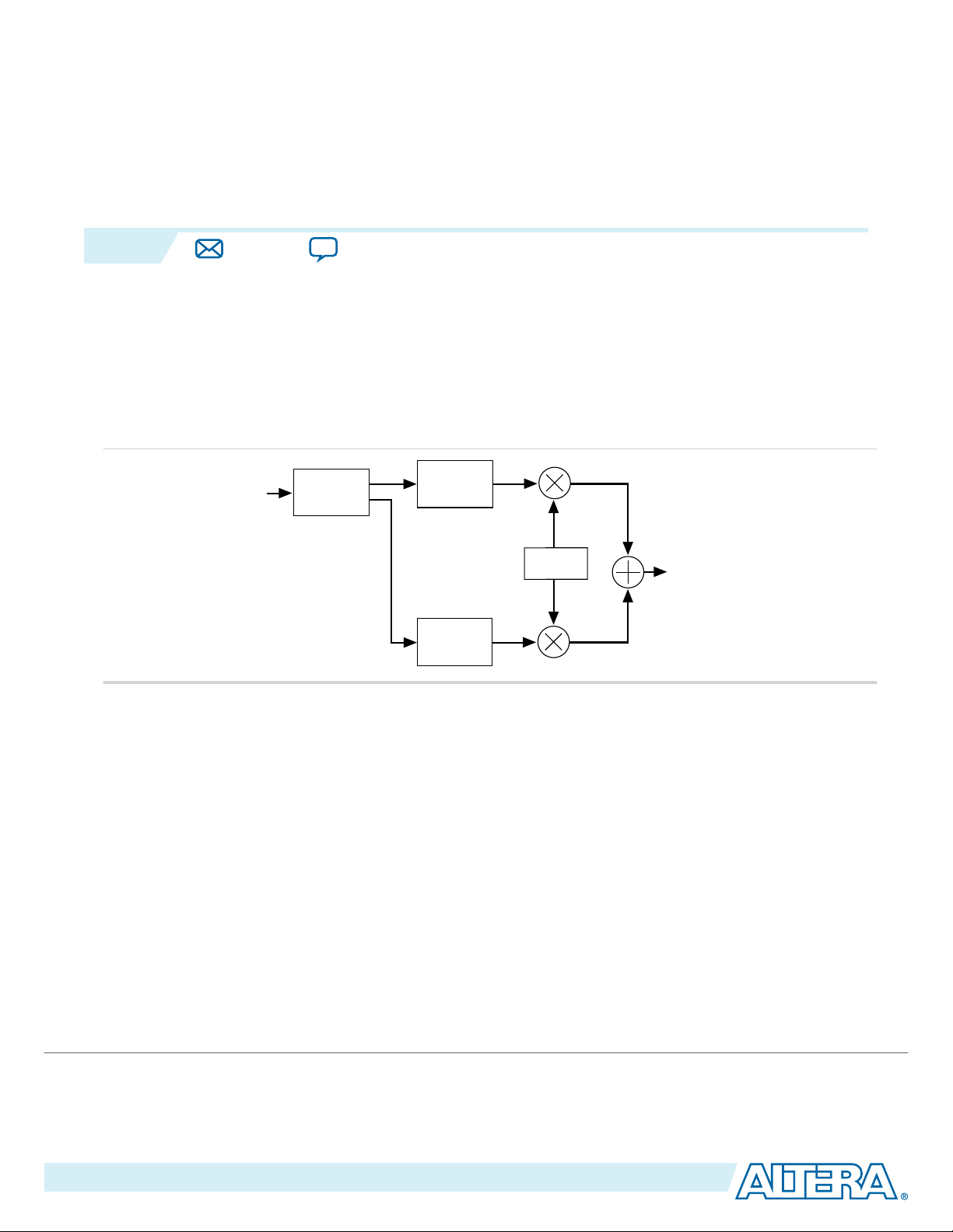
The Altera® NCO IP core generates numerically controlled oscillators (NCOs) customized for Altera
devices. A numerically controlled oscillator (NCO) synthesizes a discrete-time, discrete-valued
representation of a sinusoidal waveform.
Typically, you can use NCOs in communication systems as quadrature carrier generators in I-Q mixers,
in which baseband data is modulated onto the orthogonal carriers in one of a variety of ways.
Figure 1-1: Simple Modulator
You can also use NCOs in all-digital phase-locked-loops (PLLs) for carrier synchronization in communi‐
cations receivers, or as standalone frequency shift keying (FSK) or phase shift keying (PSK) modulators.
In these applications, the phase or the frequency of the output waveform varies directly according to an
input data stream.
You can implement ROM-based, CORDIC-based, and multiplier-based NCO architectures,. The wizard
also includes time and frequency domain graphs that dynamically display the functionality of the NCO,
based on your parameter settings.
To decide which NCO implementation to use, consider the spectral purity, frequency resolution,
performance, throughput, and required device resources. Also, consider the trade-offs between some or
all of these parameters.
Altera DSP IP Core Features
©
2015 Altera Corporation. All rights reserved. ALTERA, ARRIA, CYCLONE, ENPIRION, MAX, MEGACORE, NIOS, QUARTUS and STRATIX words and logos are
trademarks of Altera Corporation and registered in the U.S. Patent and Trademark Office and in other countries. All other words and logos identified as
trademarks or service marks are the property of their respective holders as described at www.altera.com/common/legal.html. Altera warrants performance
of its semiconductor products to current specifications in accordance with Altera's standard warranty, but reserves the right to make changes to any
products and services at any time without notice. Altera assumes no responsibility or liability arising out of the application or use of any information,
product, or service described herein except as expressly agreed to in writing by Altera. Altera customers are advised to obtain the latest version of device
specifications before relying on any published information and before placing orders for products or services.
ISO
9001:2008
Registered
Page 5

1-2
NCO IP Core Features
• Avalon® Streaming (Avalon-ST) interfaces
• DSP Builder ready
• Testbenches to verify the IP core
• IP functional simulation models for use in Altera-supported VHDL and Verilog HDL simulators
NCO IP Core Features
• 32-bit precision for angle and magnitude
• Source interface compatible with the Avalon Interface Specification
• Multiple NCO architectures:
• Multiplier-based implementation using DSP blocks or logic elements (LEs), (single cycle and multicycle)
• Parallel or serial CORDIC-based implementation
• ROM-based implementation using embedded array blocks (EABs), embedded system blocks
(ESBs), or external ROM
• Single or dual outputs (sine/cosine)
• Variable width frequency modulation input
• Variable width phase modulation input
• User-defined frequency resolution, angular precision, and magnitude precision
• Frequency hopping
• Multichannel capability
• Simulation files and architecture-specific testbenches for VHDL, Verilog HDL and MATLAB
• Dual-output oscillator and quaternary frequency shift keying (QFSK) modulator example designs
UG-NCO
2014.12.15
DSP IP Core Device Family Support
Altera offers the following device support levels for Altera IP cores:
• Preliminary support—Altera verifies the IP core with preliminary timing models for this device family.
The IP core meets all functional requirements, but might still be undergoing timing analysis for the
device family. You can use it in production designs with caution.
• Final support—Altera verifies the IP core with final timing models for this device family. The IP core
meets all functional and timing requirements for the device family. You can use it in production
designs.
Table 1-1: DSP IP Core Device Family Support
Device Family Support
Arria® II GX Final
Arria II GZ Final
Arria V Final
Arria 10 Final
Cyclone® IV Final
Cyclone V Final
Altera Corporation
About the NCO IP Core
Send Feedback
Page 6
NCO Compiler
Wizard
Bit
Accurate
Model
Output
File
Verilog HDL
Output
File
VHDL
Output
File
Synthesis
Structure
Output
File
Perl
Script
Parameter
Sweep
Compare
Results
Testbench
All Languages
UG-NCO
2014.12.15
Device Family Support
MAX® 10 FPGA Final
Stratix® IV GT Final
Stratix IV GX/E Final
Stratix V Final
Other device families No support
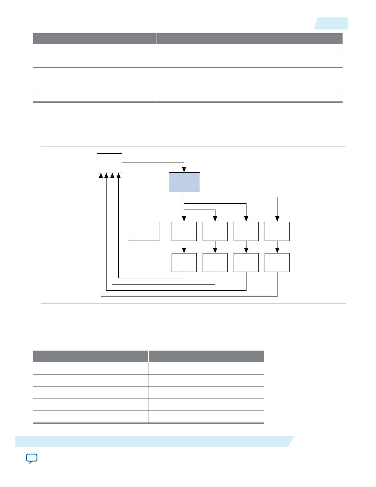
NCO IP Core MegaCore Verification
Figure 1-2: Regression Flow
NCO IP Core MegaCore Verification
1-3
NCO IP Core Release Information
Table 1-2: NCO IP Core Release Information
Version 14.1
Release Date December 2014
Ordering Code IP-NCO
Product ID(s) 0014
Vendor ID(s) 6AF7
About the NCO IP Core
Send Feedback
Item Description
Altera Corporation
Page 7

1-4
NCO IP Core Performance and Resource Utilization
Altera verifies that the current version of the Quartus II software compiles the previous version of each IP
core. Altera does not verify that the Quartus II software compiles IP core versions older than the previous
version. The Altera IP Release Notes lists any exceptions.
Related Information
• Altera IP Release Notes
• Errata for NCO IP core in the Knowledge Base
NCO IP Core Performance and Resource Utilization
Table 1-3: NCO IP Core Performance
Typical performance using the Quartus II software with the Arria V (5AGXFB3H4F40C4), Cyclone V
(5CGXFC7D6F31C6), and Stratix V (5SGSMD4H2F35C2) devices
Device Parameters ALM
DSP
Blocks
Arria V Cordic 838 0 1 -- 1,879 8 340
Memory Registers
M10K M20K Primary Secondary
(MHz)
f
MAX
UG-NCO
2014.12.15
Arria V Large Rom 56 0 12 -- 149 0 350
Arria V Multiplier
92 2 2 -- 244 2 310
Based
Arria V Small ROM 132 0 6 -- 300 0 350
CycloneVCordic 838 0 1 -- 1,881 6 260
CycloneVLarge Rom 56 0 12 -- 149 0 275
CycloneVMultiplier
92 2 2 -- 244 2 275
Based
CycloneVSmall ROM 120 0 6 -- 300 0 275
Stratix V Cordic 838 0 -- 1 1,881 6 644
Stratix V Large Rom 56 0 -- 5 149 0 700
Stratix V Multiplier
92 2 -- 2 245 1 500
Based
Stratix V Small ROM 126 0 -- 3 300 0 700
Altera Corporation
About the NCO IP Core
Send Feedback
Page 8

2014.12.15
acds
quartus - Contains the Quartus II software
ip - Contains the Altera IP Library and third-party IP cores
altera - Contains the Altera IP Library source code
<IP core name> - Contains the IP core source files
www.altera.com
101 Innovation Drive, San Jose, CA 95134
NCO IP Core Getting Started
2
UG-NCO
Subscribe
Send Feedback
1.
Installing and Licensing IP Cores
The Altera IP Library provides many useful IP core functions for your production use without purchasing
an additional license. Some Altera MegaCore® IP functions require that you purchase a separate license
for production use. However, the OpenCore® feature allows evaluation of any Altera IP core in simulation
and compilation in the Quartus® II software. After you are satisfied with functionality and perfformance,
visit the Self Service Licensing Center to obtain a license number for any Altera product.
Figure 2-1: IP Core Installation Path
Note:
The default IP installation directory on Windows is <drive>:\altera\<version number>; on Linux it is
<home directory>/altera/ <version number>.
Related Information
• Altera Licensing Site
• Altera Software Installation and Licensing Manual
OpenCore Plus IP Evaluation
Altera's free OpenCore Plus feature allows you to evaluate licensed MegaCore IP cores in simulation and
hardware before purchase. You need only purchase a license for MegaCore IP cores if you decide to take
your design to production. OpenCore Plus supports the following evaluations:
©
2015 Altera Corporation. All rights reserved. ALTERA, ARRIA, CYCLONE, ENPIRION, MAX, MEGACORE, NIOS, QUARTUS and STRATIX words and logos are
trademarks of Altera Corporation and registered in the U.S. Patent and Trademark Office and in other countries. All other words and logos identified as
trademarks or service marks are the property of their respective holders as described at www.altera.com/common/legal.html. Altera warrants performance
of its semiconductor products to current specifications in accordance with Altera's standard warranty, but reserves the right to make changes to any
products and services at any time without notice. Altera assumes no responsibility or liability arising out of the application or use of any information,
product, or service described herein except as expressly agreed to in writing by Altera. Altera customers are advised to obtain the latest version of device
specifications before relying on any published information and before placing orders for products or services.
ISO
9001:2008
Registered
Page 9

2-2
NCO IP Core OpenCore Plus Timeout Behavior
• Simulate the behavior of a licensed IP core in your system.
• Verify the functionality, size, and speed of the IP core quickly and easily.
• Generate time-limited device programming files for designs that include IP cores.
• Program a device with your IP core and verify your design in hardware.
OpenCore Plus evaluation supports the following two operation modes:
• Untethered—run the design containing the licensed IP for a limited time.
• Tethered—run the design containing the licensed IP for a longer time or indefinitely. This requires a
connection between your board and the host computer.
Note: All IP cores that use OpenCore Plus time out simultaneously when any IP core in the design times
out.
NCO IP Core OpenCore Plus Timeout Behavior
All IP cores in a device time out simultaneously when the most restrictive evaluation time is reached. If
there is more than one IP core in a design, the time-out behavior of the other IP cores may mask the timeout behavior of a specific IP core .
All IP cores in a device time out simultaneously when the most restrictive evaluation time is reached. If
there is more than one IP core in a design, a specific IP core's time-out behavior may be masked by the
time-out behavior of the other IP cores. For IP cores, the untethered time-out is 1 hour; the tethered timeout value is indefinite. Your design stops working after the hardware evaluation time expires. The Quartus
II software uses OpenCore Plus Files (.ocp) in your project directory to identify your use of the OpenCore
Plus evaluation program. After you activate the feature, do not delete these files..
UG-NCO
2014.12.15
When the evaluation time expires, the output of NCO IP core goes low.
Related Information
• AN 320: OpenCore Plus Evaluation of Megafunctions
IP Catalog and Parameter Editor
The Quartus II IP Catalog (Tools > IP Catalog) and parameter editor help you easily customize and
integrate IP cores into your project. You can use the IP Catalog and parameter editor to select, customize,
and generate files representing your custom IP variation.
Note:
The IP Catalog (Tools > IP Catalog) and parameter editor replace the MegaWizard™ Plug-In
Manager for IP selection and parameterization, beginning in Quartus II software version 14.0. Use
the IP Catalog and parameter editor to locate and paramaterize Altera IP cores.
The IP Catalog lists installed IP cores available for your design. Double-click any IP core to launch the
parameter editor and generate files representing your IP variation. The parameter editor prompts you to
specify an IP variation name, optional ports, and output file generation options. The parameter editor
generates a top-level Qsys system file (.qsys) or Quartus II IP file (.qip) representing the IP core in your
project. You can also parameterize an IP variation without an open project.
Altera Corporation
NCO IP Core Getting Started
Send Feedback
Page 10
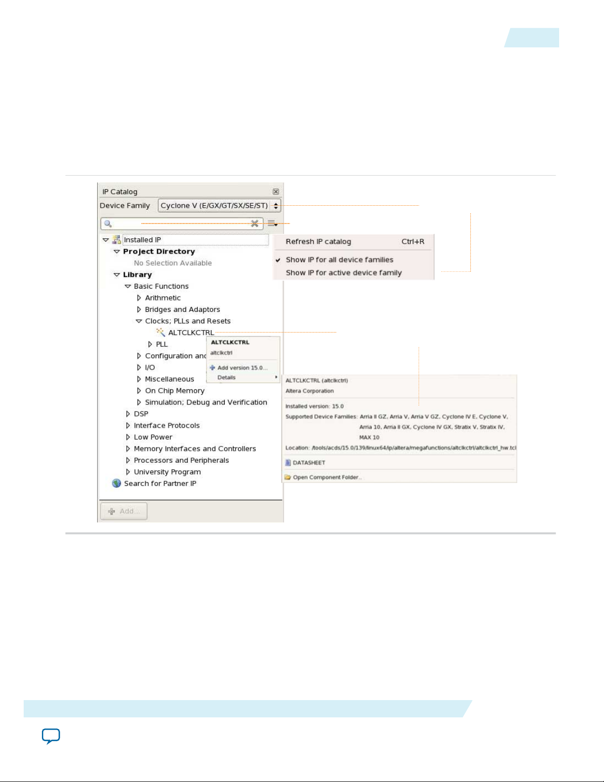
Search for installed IP cores
Double-click to customize, right-click for
detailed information
Show IP only for target device
UG-NCO
2014.12.15
Specifying IP Core Parameters and Options
Use the following features to help you quickly locate and select an IP core:
• Filter IP Catalog to Show IP for active device family or Show IP for all device families. If you have no
project open, select the Device Family in IP Catalog.
• Type in the Search field to locate any full or partial IP core name in IP Catalog.
• Right-click an IP core name in IP Catalog to display details about supported devices, open the IP core's
installation folder, and view links to documentation.
• Click Search for Partner IP, to access partner IP information on the Altera website.
Figure 2-2: Quartus II IP Catalog
2-3
Note: The IP Catalog is also available in Qsys (View > IP Catalog). The Qsys IP Catalog includes
exclusive system interconnect, video and image processing, and other system-level IP that are not
available in the Quartus II IP Catalog. For more information about using the Qsys IP Catalog, refer
to Creating a System with Qsys in the Quartus II Handbook.
Specifying IP Core Parameters and Options
You can quickly configure a custom IP variation in the parameter editor. Use the following steps to
specify IP core options and parameters in the parameter editor. Refer to Specifying IP Core Parameters
and Options (Legacy Parameter Editors) for configuration of IP cores using the legacy parameter editor.
NCO IP Core Getting Started
Send Feedback
Altera Corporation
Page 11

2-4
Specifying IP Core Parameters and Options
UG-NCO
2014.12.15
1. In the IP Catalog (Tools > IP Catalog), locate and double-click the name of the IP core to customize.
The parameter editor appears.
2. Specify a top-level name for your custom IP variation. The parameter editor saves the IP variation
settings in a file named <your_ip>.qsys. Click OK.
3. Specify the parameters and options for your IP variation in the parameter editor, including one or
more of the following. Refer to your IP core user guide for information about specific IP core
parameters.
• Optionally select preset parameter values if provided for your IP core. Presets specify initial
parameter values for specific applications.
• Specify parameters defining the IP core functionality, port configurations, and device-specific
features.
• Specify options for processing the IP core files in other EDA tools.
4. Click Generate HDL, the Generation dialog box appears.
5. Specify output file generation options, and then click Generate. The IP variation files generate
according to your specifications.
6. To generate a simulation testbench, click Generate > Generate Testbench System.
7. To generate an HDL instantiation template that you can copy and paste into your text editor, click
Generate > HDL Example.
8. Click Finish. The parameter editor adds the top-level .qsys file to the current project automatically. If
you are prompted to manually add the .qsys file to the project, click Project > Add/Remove Files in
Project to add the file.
9. After generating and instantiating your IP variation, make appropriate pin assignments to connect
ports.
Altera Corporation
NCO IP Core Getting Started
Send Feedback
Page 12

View IP port
and parameter
details
Apply preset parameters for
specific applications
Specify your IP variation name
and target device
UG-NCO
2014.12.15
Figure 2-3: IP Parameter Editor
Files Generated for Altera IP Cores
2-5
Files Generated for Altera IP Cores
The Quartus II software generates the following IP core output file structure:
NCO IP Core Getting Started
Send Feedback
Altera Corporation
Page 13

<your_testbench>_tb.csv
<your_testbench>_tb.spd
<your_ip>.cmp - VHDL component declaration file
<your_ip>.ppf - XML I/O pin information file
<your_ip>.qip - Lists IP synthesis files
<your_ip>.sip - Contains assingments for IP simulation files
<your_ip>.v or .vhd
Top-level IP synthesis file
<your_ip>.v or .vhd
Top-level simulation file
<simulator_setup_scripts>
<your_ip>.qsys - System or IP integration file
<your_ip>_bb.v - Verilog HDL black box EDA synthesis file
<your_ip>_inst.v or .vhd - Sample instantiation template
<your_ip>_generation.rpt - IP generation report
<your_ip>.debuginfo - Contains post-generation information
<your_ip>.html - Connection and memory map data
<your_ip>.bsf - Block symbol schematic
<your_ip>.spd - Combines simulation scripts for multiple cores
<your_ip>_tb.qsys
Testbench system file
<your_ip>.sopcinfo - Software tool-chain integration file
<project directory>
<EDA tool setup
scripts>
<your_ip>
IP variation files
<testbench>_tb
testbench system
sim
Simulation files
synth
IP synthesis files
sim
simulation files
<EDA tool name>
Simulator scripts
<testbench>_tb
<ip subcores> n
Subcore libraries
sim
Subcore
Simulation files
synth
Subcore
synthesis files
<HDL files>
<HDL files>
<your_ip> n
IP variation files
testbench files
2-6
Files Generated for Altera IP Cores
Figure 2-4: IP Core Generated Files
UG-NCO
2014.12.15
Altera Corporation
Table 2-1: IP Core Generated Files
File Name Description
<my_ip>.qsys
<system>.sopcinfo Describes the connections and IP component parameterizations in
The Qsys system or top-level IP variation file. <my_ip> is the name
that you give your IP variation.
your Qsys system. You can parse its contents to get requirements
when you develop software drivers for IP components.
Downstream tools such as the Nios II tool chain use this file.
The .sopcinfo file and the system.h file generated for the Nios II tool
chain include address map information for each slave relative to each
master that accesses the slave. Different masters may have a different
address map to access a particular slave component.
NCO IP Core Getting Started
Send Feedback
Page 14

UG-NCO
2014.12.15
Files Generated for Altera IP Cores
File Name Description
<my_ip>.cmp The VHDL Component Declaration (.cmp) file is a text file that
contains local generic and port definitions that you can use in VHDL
design files.
2-7
<my_ip>.html
A report that contains connection information, a memory map
showing the address of each slave with respect to each master to
which it is connected, and parameter assignments.
<my_ip>_generation.rpt IP or Qsys generation log file. A summary of the messages during IP
generation.
<my_ip>.debuginfo Contains post-generation information. Used to pass System Console
and Bus Analyzer Toolkit information about the Qsys interconnect.
The Bus Analysis Toolkit uses this file to identify debug components
in the Qsys interconnect.
<my_ip>.qip
Contains all the required information about the IP component to
integrate and compile the IP component in the Quartus II software.
<my_ip>.csv Contains information about the upgrade status of the IP component.
<my_ip>.bsf A Block Symbol File (.bsf) representation of the IP variation for use
in Quartus II Block Diagram Files (.bdf).
<my_ip>.spd
Required input file for ip-make-simscript to generate simulation
scripts for supported simulators. The .spd file contains a list of files
generated for simulation, along with information about memories
that you can initialize.
<my_ip>.ppf The Pin Planner File (.ppf) stores the port and node assignments for
IP components created for use with the Pin Planner.
<my_ip>_bb.v You can use the Verilog black-box (_bb.v) file as an empty module
declaration for use as a black box.
<my_ip>.sip Contains information required for NativeLink simulation of IP
components. You must add the .sip file to your Quartus project.
<my_ip>_inst.v or _inst.vhd HDL example instantiation template. You can copy and paste the
contents of this file into your HDL file to instantiate the IP variation.
<my_ip>.regmap If the IP contains register information, the .regmap file generates.
The .regmap file describes the register map information of master
and slave interfaces. This file complements the .sopcinfo file by
providing more detailed register information about the system. This
enables register display views and user customizable statistics in
System Console.
NCO IP Core Getting Started
Send Feedback
Altera Corporation
Page 15

2-8
Simulating Altera IP Cores in other EDA Tools
File Name Description
UG-NCO
2014.12.15
<my_ip>.svd
<my_ip>.v
or
<my_ip>.vhd
mentor/
aldec/
/synopsys/vcs
/synopsys/vcsmx
Allows HPS System Debug tools to view the register maps of
peripherals connected to HPS within a Qsys system.
During synthesis, the .svd files for slave interfaces visible to System
Console masters are stored in the .sof file in the debug section.
System Console reads this section, which Qsys can query for register
map information. For system slaves, Qsys can access the registers by
name.
HDL files that instantiate each submodule or child IP core for
synthesis or simulation.
Contains a ModelSim® script msim_setup.tcl to set up and run a
simulation.
Contains a Riviera-PRO script rivierapro_setup.tcl to setup and run a
simulation.
Contains a shell script vcs_setup.sh to set up and run a VCS
®
simulation.
Contains a shell script vcsmx_setup.sh and synopsys_ sim.setup file to
set up and run a VCS MX® simulation.
/cadence
Contains a shell script ncsim_setup.sh and other setup files to set up
and run an NCSIM simulation.
/submodules Contains HDL files for the IP core submodule.
<child IP cores>/ For each generated child IP core directory, Qsys generates /synth and /
sim sub-directories.
Simulating Altera IP Cores in other EDA Tools
The Quartus II software supports RTL and gate-level design simulation of Altera IP cores in supported
EDA simulators. Simulation involves setting up your simulator working environment, compiling
simulation model libraries, and running your simulation.
You can use the functional simulation model and the testbench or example design generated with your IP
core for simulation. The functional simulation model and testbench files are generated in a project
subdirectory. This directory may also include scripts to compile and run the testbench. For a complete list
of models or libraries required to simulate your IP core, refer to the scripts generated with the testbench.
You can use the Quartus II NativeLink feature to automatically generate simulation files and scripts.
NativeLink launches your preferred simulator from within the Quartus II software.
Altera Corporation
NCO IP Core Getting Started
Send Feedback
Page 16

Post-fit timing
simulation netlist
Post-fit timing
simulation (3)
Post-fit functional
simulation netlist
Post-fit functional
simulation
Analysis & Synthesis
Fitter
(place-and-route)
TimeQuest Timing Analyzer
Device Programmer
Quartus II
Design Flow
Gate-Level Simulation
Post-synthesis
functional
simulation
Post-synthesis functional
simulation netlist
(Optional) Post-fit
timing simulation
RTL Simulation
Design Entry
(HDL, Qsys, DSP Builder)
Altera Simulation
Models
EDA
Netlist
Writer
UG-NCO
2014.12.15
Figure 2-5: Simulation in Quartus II Design Flow
DSP Builder Design Flow
2-9
Note: Post-fit timing simulation is supported only for Stratix IV and Cyclone IV devices in the current
version of the Quartus II software. Altera IP supports a variety of simulation models, including
simulation-specific IP functional simulation models and encrypted RTL models, and plain text
RTL models. These are all cycle-accurate models. The models support fast functional simulation of
your IP core instance using industry-standard VHDL or Verilog HDL simulators. For some cores,
only the plain text RTL model is generated, and you can simulate that model. Use the simulation
models only for simulation and not for synthesis or any other purposes. Using these models for
synthesis creates a nonfunctional design.
Related Information
Simulating Altera Designs
DSP Builder Design Flow
DSP Builder shortens digital signal processing (DSP) design cycles by helping you create the hardware
representation of a DSP design in an algorithm-friendly development environment.
This IP core supports DSP Builder. Use the DSP Builder flow if you want to create a DSP Builder model
that includes an IP core variation; use IP Catalog if you want to create an IP core variation that you can
instantiate manually in your design. For more information about the DSP Builder flow, refer to the
NCO IP Core Getting Started
Send Feedback
Altera Corporation
Page 17

2-10
DSP Builder Design Flow
Related Information
Using MegaCore Functions chapter in the DSP Builder Handbook.
UG-NCO
2014.12.15
Altera Corporation
NCO IP Core Getting Started
Send Feedback
Page 18

2014.12.15
sine
cosine
f
INC
f
FM
Internal
Dither
f
DITH
Waveform
Generation
Unit
Phase Accumulator
Phase
Increment
Frequency
Modulation
Input
f
PM
Phase
Modulation
Input
Dither
Generator
D
Required
Optional
www.altera.com
101 Innovation Drive, San Jose, CA 95134
NCO IP Core Functional Description
3
UG-NCO
Subscribe
Send Feedback
Figure 3-1: NCO Block Diagram
The NCO IP core allows you to generate a variety of NCO architectures. Your custom NCO includes both
time- and frequency-domain analysis tools. The custom NCO outputs a sinusoidal waveform in two's
complement representation.
The waveform for the generated sine wave is defined by the following equation:
s(nT) = A sin[2π(fO + fFM)nT + ϕPM + ϕ
DITH
)]
where:
• T is the operating clock period
• fO is the unmodulated output frequency based on the input value ϕ
• fFM is a frequency modulating parameter based on the input value ϕ
• ϕPM is derived from the phase modulation input value P and the number of bits (P
value by the equation: ϕPM = P/2^P
• ϕ
• A is 2N-1 where N is the magnitude precision (and N is an integer in the range 10 to 32
The generated output frequency, fo for a given phase increment, ϕ
ϕ
incfclk
©
2015 Altera Corporation. All rights reserved. ALTERA, ARRIA, CYCLONE, ENPIRION, MAX, MEGACORE, NIOS, QUARTUS and STRATIX words and logos are
trademarks of Altera Corporation and registered in the U.S. Patent and Trademark Office and in other countries. All other words and logos identified as
trademarks or service marks are the property of their respective holders as described at www.altera.com/common/legal.html. Altera warrants performance
of its semiconductor products to current specifications in accordance with Altera's standard warranty, but reserves the right to make changes to any
products and services at any time without notice. Altera assumes no responsibility or liability arising out of the application or use of any information,
product, or service described herein except as expressly agreed to in writing by Altera. Altera customers are advised to obtain the latest version of device
specifications before relying on any published information and before placing orders for products or services.
is the internal dithering value
DITH
/2M Hz
width
INC
FM
) used for this
width
is determined by the equation: f0 =
inc
ISO
9001:2008
Registered
Page 19

3-2
NCO IP Core Architectures
UG-NCO
2014.12.15
where M is the accumulator precision and f
The minimum possible output frequency waveform is generated for the case where ϕ
is the clock frequency
clk
= 1. This case is
inc
also the smallest observable frequency at the output of the NCO, also known as the frequency resolution
of the NCO, f
f
= f
RES
clk
given in Hz by the equation:
res
/2M Hz
For example, if a 100 MHz clock drives an NCO with an accumulator precision of 32 bits, the frequency
resolution of the oscillator is 0.0233 Hz. For an output frequency of 6.25 MHz from this oscillator, you
should apply an input phase increment of:
(6.25 x 10⁶/100 x 106) x 232 = 268435456
The NCO MegaCore function automatically calculates this value, using the specified parameters. IP
Toolbench also sets the value of the phase increment in all testbenches and vector source files it generates.
Similarly, the generated output frequency, fFM for a given frequency modulation increment, ϕFM is
determined by the equation:
fFM = ϕFMf
/2F Hz
clk
where F is the modulator resolution
The angular precision of an NCO is the phase angle precision before the polar-to-cartesian transforma‐
tion. The magnitude precision is the precision to which the sine and/or cosine of that phase angle can be
represented. The effects of reduction or augmentation of the angular, magnitude, accumulator precision
on the synthesized waveform vary across NCO architectures and for different fo/f
clk
ratios.
You can view these effects in the NCO time and frequency domain graphs as you change the NCO IP core
parameters.
NCO IP Core Architectures
The NCO MegaCore function supports large ROM, small ROM, CORDIC, and multiplier-based
architectures.
Large ROM Architecture
Use the large ROM architecture if your design requires very high speed sinusoidal waveforms and your
design can use large quantities of internal memory.
In this architecture, the ROM stores the full 360 degrees of both the sine and cosine waveforms. The
output of the phase accumulator addresses the ROM.
The internal memory holds all possible output values for a given angular and magnitude precision. The
generated waveform has the highest spectral purity for that parameter set (assuming no dithering). The
large ROM architecture also uses the fewest logic elements (LEs) for a given set of precision parameters.
Small ROM Architecture
To reduce LE usage and increase output frequency, use the small ROM architecture.
In a small ROM architecture, the device memory only stores 45 degrees of the sine and cosine waveforms.
All other output values are derived from these values based on the position of the rotating phasor on the
unit circle.
Altera Corporation
NCO IP Core Functional Description
Send Feedback
Page 20

UG-NCO
2014.12.15
Table 3-1: Derivation of Output Values
CORDIC Architecture
3-3
Position in Unit
Circle
Range for Phase x sin(x) cos(x)
1 0 <= x < π/4 sin(x) cos(x)
2 π/4 <= x < π/2 cos(π/4x) sin(π/2-x)
3 π/2 <= x < 3π/4 cos(x-π/2) -sin(x-π/2)
4 3π/4 <= x < π sin(π-x) -cos(π-x)
5 π <= x < 5π/4 -sin(x-π) -cos(x-π)
6 5π/4 <= x < 3π/2 -cos(3π/2-x) -sin(3π/2-x)
7 3π/2 <= x < 7π/4 -cos(x-3π/2) sin(x-3π/2)
8 7π/4 <= x < 2π -sin(2π-x) cos(2π-x)
A small ROM implementation is more likely to have periodic value repetition, so the resulting waveform's
SFDR is lower than that of the large ROM architecture. However, you can often mitigate this reduction in
SFDR by using phase dithering.
Figure 3-2: Derivation of output Values
Related Information
Phase Dithering on page 3-6
CORDIC Architecture
The CORDIC algorithm, which can calculate trigonometric functions such as sine and cosine, provides a
high-performance solution for very-high precision oscillators in systems where internal memory is at a
premium.
The CORDIC algorithm is based on the concept of complex phasor rotation by multiplication of the
phase angle by successively smaller constants. In digital hardware, the multiplication is by powers of two
NCO IP Core Functional Description
Send Feedback
Altera Corporation
Page 21

ø
sin ø
cos ø
y
x
dø
dx
dy
3-4
Multiplier-Based Architecture
only. Therefore, the algorithm can be implemented efficiently by a series of simple binary shift and
additions/subtractions.
In an NCO, the CORDIC algorithm computes the sine and cosine of an input phase value by iteratively
shifting the phase angle to approximate the cartesian coordinate values for the input angle. At the end of
the CORDIC iteration, the x and y coordinates for a given angle represent the cosine and sine of that
angle, respectively.
Figure 3-3: CORDIC Rotation for Sine & Cosine Calculation
UG-NCO
2014.12.15
With the NCO MegaCore function, you can select parallel (unrolled) or serial (iterative) CORDIC
architectures:
• You an use the parallel CORDIC architecture to create a very high-performance, high-precision
oscillator—implemented entirely in logic elements—with a throughput of one output sample per clock
cycle. With this architecture, there is a new output value every clock cycle.
• The serial CORDIC architecture uses fewer resources than the parallel CORDIC architecture.
However, its throughput is reduced by a factor equal to the magnitude precision. For example, if you
select a magnitude precision of N bits in the NCO MegaCore function, the output sample rate and the
Nyquist frequency is reduced by a factor of N. This architecture is implemented entirely in logic
elements and is useful if your design requires low frequency, high precision waveforms. With this
architecture, the adder stages are stored internally and a new output value is produced every N clock
cycles.
Multiplier-Based Architecture
The multiplier-based architecture uses multipliers to reduce memory usage. You can choose to implement
the multipliers in either:
• Logic elements (Cyclone series) or combinational ALUTs (Stratix series).
• Dedicated multiplier circuitry (for example, dedicated DSP blocks) (Stratix or Arria series).
Note:
When you specify a dual output multiplier-based NCO, the IP core provides an option to output a
sample every two clock cycles. This setting reduces the throughput by a factor of two and halves the
resources required by the waveform generation unit.
Altera Corporation
NCO IP Core Functional Description
Send Feedback
Page 22

UG-NCO
2014.12.15
Table 3-2: Architecture Comparison
Architecture Advantages
Multichannel NCOs
3-5
Large
ROM
Small
ROM
CORDIC High performance solution when internal memory is at a
Multiplier
-Based
Multichannel NCOs
The NCO IP core allows you to implement multichannel NCOs. You can generate multiple sinusoids of
independent frequency and phase t at a very low cost in additional resources. The waveforms have an
output sample-rate of f
Multichannel implementations are available for all single-cycle generation algorithms. The input phase
increment, frequency modulation value and phase modulation input are input sequentially to the NCO
with the input values corresponding to channel 0 first and channel (M–1) last. The inputs to channel 0
should be input on the rising clock edge immediately following the de-assertion of the NCO reset.
Good for high speed and when a large quantity of internal
memory is available. Gives the highest spectral purity and uses
the fewest logic elements for a given parameterization.
Good for high output frequencies with reduced internal memory
usage when a lower SFDR is acceptable.
premium. The serial CORDIC architecture uses fewer resources
than parallel although the throughput is reduced.
Reduced memory usage by implementing multipliers in logic
elements or dedicated circuitry.
/M where M is the number of channels. You can select 1 to 8 channels.
clk
On the output side, the first output sample for channel 0 is output concurrent with the assertion of
out_valid and the remaining outputs for channels 1 to (M–1) are output sequentially.
If you select a multichannel implementation, the NCO MegaCore function generates VHDL and Verilog
HDL testbenches that time-division-multiplex the inputs into a single stream and demultiplex the output
streams into their respective downsampled channelized outputs.
Related Information
NCO Multichannel Design Example on page 4-1
Frequency Hopping
The NCO IP core supports frequency hopping (except the serial CORDIC architecture). Frequency
hopping allows control and configuration of the NCO IP core at run time so that carriers with different
frequencies can be generated and held for a specified period of time at specified slot intervals.
The IP core supports multiple phase increment registers that you can load using an Avalon-MM bus. You
select the phase increment register using an external hardware signal; changes on this signal take effect on
the next clock cycle. The maximum number of phase increment registers is 16.
Note:
During frequency hopping, the phase of the carrier should not experience discontinuous change.
Discontinuous carrier phase changes may cause spectral emission problems.
NCO IP Core Functional Description
Send Feedback
Altera Corporation
Page 23

Numerically
Controlled
Oscillator
fcos_o
out_valid
Avalon-MM
Interface
clk
reset_n
reset_n
address
write_sig
increment
freq_sel_sig
16 to 1
MUX
clken
RAM
fsin_0
phi_inc_i
clken
clk
NCO MegaCore Function
3-6
Phase Dithering
Figure 3-4: Frequency Hopping Block Diagram
The RAM stores all hopping frequencies. The RAM size is <width>×<depth>, where <width> is the
number of bits required to specify the phase accumulator value to the precision you select in the
parameter editor, and <depth> is the number of bands you select in the parameter editor.
UG-NCO
2014.12.15
Altera Corporation
Phase Dithering
All digital sinusoidal synthesizers suffer from the effects of finite precision, which manifests itself as spurs
in the spectral representation of the output sinusoid. Because of angular precision limitations, the derived
phase of the oscillator tends to be periodic in time and contributes to the presence of spurious frequencies.
You can reduce the noise at these frequencies by introducing a random signal of suitable variance into the
derived phase, thereby reducing the likelihood of identical values over time. Adding noise into the data
path raises the overall noise level within the oscillator, but tends to reduce the noise localization and can
provide significant improvement in SFDR.
The extent to which you can reduce spur levels is dependent on many factors. The likelihood of repetition
of derived phase values and resulting spurs, for a given angular precision, is closely linked to the ratio of
the clock frequency to the desired output frequency. An integral ratio clearly results in high-level spurious
frequencies, while an irrational relationship is less likely to result in highly correlated noise at harmonic
frequencies.
The Altera NCO IP core allows you to finely tune the variance of the dither sequence for your chosen
algorithm, specified precision, and clock frequency to output frequency ratio, and dynamically view the
effects on the output spectrum graphically.
Related Information
NCO Multichannel Design Example on page 4-1
NCO IP Core Functional Description
Send Feedback
Page 24

UG-NCO
2014.12.15
Frequency Modulation
You can add an optional frequency modulator to your custom NCO variation. You can use the frequency
modulator to vary the oscillator output frequency about a center frequency set by the input phase
increment. This option is useful for applications in which the output frequency is tuned relative to a freerunning frequency, for example in all-digital phase-lock-loops.
You can also use the frequency modulation input to switch the output frequency directly.
You can set the frequency modulation resolution input in the IP core. The specified value must be less
than or equal to the phase accumulator precision.
The NCO IP core also provides an option to increase the modulator pipeline level; however, the effect of
the increase on the performance of the NCO IP core varies across NCO architectures and variations.
Phase Modulation
You can use the NCO IP core to add an optional phase modulator to your variation, allowing dynamic
phase shifting of the NCO output waveforms. This option is particularly useful if you want an initial phase
offset in the output sinusoid.
Frequency Modulation
3-7
You can also use the option to implement efficient phase shift keying (PSK) modulators in which the
input to the phase modulator varies according to a data stream. You set the resolution and pipeline level
of the phase modulator in the NCO wizard. The input resolution must be greater than or equal to the
specified angular precision.
NCO IP Core Parameters
The wizard only allows you to select legal combinations of parameters, and warns you of any invalid
configurations.
Architecture Parameters
Table 3-3: Architecture Parameters
Parameter Value Description
Generation
Algorithm
Outputs Dual Output, Single
Device Family
Target
Small ROM, Large
ROM, CORDIC,
Multiplier-Based
Output
— Displays the target device family. The target device
Select the required algorithm.
Select whether to use a dual or single output.
family is preselected by the value specified in the
Quartus II or DSP Builder software. The HDL that
is generated for your variation may be incorrect if
you change the device family target in this wizard.
Number of
Channels
NCO IP Core Functional Description
Send Feedback
1–8 Select the number of channels when you want to
implement a multichannel NCO.
Altera Corporation
Page 25

3-8
Frequency Parameters
Parameter Value Description
Number of Bands 1–16 Select a number of bands greater than 1 to enable
frequency hopping. Frequency hopping is not
supported in the serial CORDIC architecture.
UG-NCO
2014.12.15
Use dedicated
On or off When the multiplier-based algorithm is selected on
multipliers
CORDIC
Parallel, Serial When you select the CORDIC generation
Implementation
Clock Cycles Per
1, 2. When the multiplier-based algorithm is selected on
Output
Related Information
NCO IP Core Architectures on page 3-2
Frequency Parameters
Table 3-4: Frequency Parameters
Parameter Value Description
the Parameters page, turn on to use dedicated
multipliers and select the number of clock cycles
per output, otherwise the design uses logic
elements. This option is not available if you target
the Cyclone device family.
algorithm, you can select a parallel (one output per
clock cycle) or serial (one output per 18 clock
cycles) implementation.
the Parameters page, you can select 1 or 2 clock
cycles per output.
Phase Accumulator
Precision
4 to 64, Select the required phase accumulator precision. The
phase accumulator precision must be greater than or
equal to the specified angular resolution.
Angular Resolution 4 to 24 or 32, Select the required angular resolution. The
maximum value is 24 for small and large ROM
algorithms; 32 for CORDIC and multiplier-based
algorithms.
Magnitude Precision 10 to 32, Select the required magnitude precision.
Implement Phase
On or Off Turn on to implement phase dithering.
Dithering
Dither Level Min to Max When phase dithering is enabled you can use the
slider control to adjust the dither level between its
minimum and maximum values,
Clock Rate 1 to 999 MHz, kHz,
Hz, mHz,
Desired Output
Frequency
Phase Increment
1 to 999 MHz, kHz,
Hz, mHz,
— Displays the phase increment value calculated from
Value
Select the clock rate using units of MegaHertz,
kiloHertz, Hertz or milliHertz.
Select the desired output frequency using units of
MegaHertz, kiloHertz, Hertz or milliHertz.
the clock rate and desired output frequency.
Altera Corporation
NCO IP Core Functional Description
Send Feedback
Page 26

UG-NCO
2014.12.15
Optional Ports Parameters
Parameter Value Description
3-9
Real Output
— Displays the calculated value of the real output
Frequency
Related Information
• Frequency Modulation on page 3-7
• Phase Modulation on page 3-7
Optional Ports Parameters
Table 3-5: Optional Ports Parameters
Parameter Value Description
Frequency
Modulation input
Modulator
Resolution
Modulator Pipeline
Level
Phase Modulation
Input
On or Off You can optionally enable the frequency modulation
4 to 64, Select the modulator resolution for the frequency
1, 2, Select the modulator pipeline level for the frequency
On or Off You can optionally enable the phase modulation input.
frequency.
input.
modulation input.
modulation input.
Modulator
Precision
Modulator Pipeline
Level
4 to 32, Select the modulator precision for the phase
modulation input.
1, 2, Select the modulator pipeline level for the phase
modulation input.
NCO IP Core Interfaces and Signals
The NCO MegaCore function is an Avalon-ST source and does not support backpressure.The AvalonMM interface allows you to control frequency hopping at run time.
Related Information
Avalon Interface Specifications
For more information about the Avalon-MM and Avalon-ST interfaces including integration with other
Avalon-ST components which may support backpressure
Avalon-ST Interfaces in DSP IP Cores
Avalon-ST interfaces define a standard, flexible, and modular protocol for data transfers from a source
interface to a sink interface.
The input interface is an Avalon-ST sink and the output interface is an Avalon-ST source. The Avalon-ST
interface supports packet transfers with packets interleaved across multiple channels.
Avalon-ST interface signals can describe traditional streaming interfaces supporting a single stream of
data without knowledge of channels or packet boundaries. Such interfaces typically contain data, ready,
NCO IP Core Functional Description
Send Feedback
Altera Corporation
Page 27

3-10
NCO IP Core Signals
and valid signals. Avalon-ST interfaces can also support more complex protocols for burst and packet
transfers with packets interleaved across multiple channels. The Avalon-ST interface inherently synchro‐
nizes multichannel designs, which allows you to achieve efficient, time-multiplexed implementations
without having to implement complex control logic.
Avalon-ST interfaces support backpressure, which is a flow control mechanism where a sink can signal to
a source to stop sending data. The sink typically uses backpressure to stop the flow of data when its FIFO
buffers are full or when it has congestion on its output.
Related Information
• Avalon Interface Specifications
NCO IP Core Signals
Table 3-6: NCO IP Core Signals
UG-NCO
2014.12.15
Signal Directio
n
address[2:0] Input Address of the 16 phase increment registers when frequency
Description
hopping is enabled.
clk Input Clock.
clken Input Active-high clock enable.
freq_mod_i [F-
1:0]
freq_sel[log
2
1:0]
N-
Input Optional frequency modulation input. You can specify the
modulator resolution F in IP Toolbench.
input Use to select one of the phase increment registers (that is to
select the hopping frequencies), when frequency hopping is
enabled. N is the depth.
phase_mod_i [P1:0]
phi_inc_i [A-1:0] Input Input phase increment. You can specify the accumulator
Input Optional phase modulation input. You can specify the
modulator precision P in Ithe wizard.
precision A in the wizard.
reset_n Input Active-low asynchronous reset.
write_sig Input Active-high write signal when frequency hopping is enabled.
in_data Output In Qsys systems, this Avalon-ST-compliant data bus includes all
the Avalon-ST input data signals.
fcos_o [M-1:0] Output Optional output cosine value (when dual output is selected). You
fsin_o [M-1:0] Output Output sine value. You can specify the magnitude precision M in
out_valid Output Data valid signal. Asserted by the MegaCore function when there
out_data Output In Qsys systems, this Avalon-ST-compliant data bus includes all
Altera Corporation
can specify the magnitude precision M in IP Toolbench.
IP Toolbench.
is valid data to output.
the Avalon-ST output data signals.
NCO IP Core Functional Description
Send Feedback
Page 28

clk
clken
phi_inc_i
reset_n
fsin_0
fcos_0
out_valid
42949673
0 -3 2057 41... 61.... 8148 10... 12... 13.... 15...
0 32767 32... 32... 32... 32... 31... 31... 30... 29... 28
clk
clken
reset_n
fsin_0
fcos_0
out_valid
0 -3 41... 81... 12.... 15... 19... 22... 25...
0 32766 32... 32... 31... 30... 28... 26... 23... 20...
phi_inc_i
85899346
27... 29... 31... 32.... 32... 32... 32...
17... 13... 10... 61.... 20... -2... -6...
31...
-1...
29...
-1...
clk
clken
reset_n
fsin_0
fcos_0
out_valid
0 3 1404
0 2047
phi_inc_i
31457
-20112043 1574 257 -1201
1490 -383129 -1308 -2030 -16572046
UG-NCO
2014.12.15
NCO IP Core Timing Diagrams
Figure 3-5: Single-Cycle Per Output Timing Diagram
All NCO architectures, except for serial CORDIC and multi-cycle multiplier-based architectures, output a
sample every clock cycle. After the clock enable is asserted, the oscillator outputs the sinusoidal samples at
a rate of one sample per clock cycle, following an initial latency of L clock cycles. The exact value of L
varies across architectures and parameterizations.
Note:
For the non-single-cycle per output architectures, the optional phase and frequency modulation
inputs need to be valid at the same time as the corresponding phase increment value. The values
should be sampled every 2 cycles for the two-cycle multiplier-based architecture and every N cycles
for the serial CORDIC architecture, where N is the magnitude precision.
NCO IP Core Timing Diagrams
3-11
Figure 3-6: Two-Cycle Multiplier-Based Architecture Timing Diagram
After the clock enable is asserted, the oscillator outputs the sinusoidal samples at a rate of one sample for
every two clock cycles, following an initial latency of L clock cycles. The exact value of L depends on the
parameters that you set.
Figure 3-7: Serial CORDIC Timing Diagram with N = 8
The fsin_0 and fcos_0 values can change while out_valid is low.
NCO IP Core Functional Description
Note:
Send Feedback
Altera Corporation
Page 29

3-12
NCO IP Core Timing Diagrams
After the clock enable is asserted, the oscillator outputs sinusoidal samples at a rate of one sample per N
clock cycles, where N is the magnitude precision. The IP core has an initial latency of L clock cycles; the
exact value of L depends on the parameters that you set.
Table 3-7: Latency Values for Different Architectures
UG-NCO
2014.12.15
Latency
(1), (2)
Architecture Variation
Base Minimum Maximum
Small ROM all 7 7 13
Large ROM all 4 4 10
Multiplier-
Throughput = 1, Logic cells 11 11 17
Based
Multiplier-
Based
Multiplier-
Based
Multiplier-
Throughput = 1, Dedicated, Special case
(3)
Throughput = 1, Dedicated, Not special
8 8 14
10 10 16
case
Throughput = 1/2 15 15 26
Based
CORDIC Parallel 2N + 4 20
CORDIC Serial CORDIC 2N + 2 18
(4)
(6)
Figure 3-8: Multi-Channel NCO Timing Diagram with M = 4.
The IP core sequentially interleaves and loads input phase increments for each channel, P
74
258
(5)
(7)
k
The phase increment for channel 0 is the first value read in on the rising edge of the clock following the
de-assertion of reset_n (assuming clken is asserted) followed by the phase increments for the next (M-1)
channels. The output signal out_valid is asserted when the first valid sine and cosine outputs for channel
0, S0, C0, respectively are available.
(1)
Latency = base latency + dither latency+ frequency modulation pipeline + phase modulation pipeline (×N
for serial CORDIC).
(2)
Dither latency = 0 (dither disabled) or 2 (dither enabled).
(3)
Special case: (9 <= N <= 18 && WANT_SIN_AND_COS).
(4)
Minimum latency assumes N = 8.
(5)
Maximum latency assumes N = 32
(6)
Minimum latency assumes N = 8.
(7)
Maximum latency assumes N = 32
Altera Corporation
NCO IP Core Functional Description
Send Feedback
Page 30

UG-NCO
2014.12.15
NCO IP Core Timing Diagrams
3-13
The output values Sk and Ck corresponding to channels 1 through (M-1) are output sequentially by the
NCO. The outputs are interleaved so that a new output sample for channel k is available every M cycles.
NCO IP Core Functional Description
Send Feedback
Altera Corporation
Page 31

2014.12.15
Counter
phi_ch0
phi_ch1
phi_ch2
phi_ch3
fmod_ch0
fmod_ch1
fmod_ch2
fmod_ch3
pmod_ch0
pmod_ch1
pmod_ch2
pmod_ch3
sin_ch0
sin_ch1
sin_ch2
sin_ch3
cos_ch0
cos_ch1
cos_ch2
cos_ch3
startofpacket
endofpacket
valid
fsin_o
fcos_o
phi_inc_i
req_mode_i
phase_mod_i
fsin_o
fcos_o
out_valid
Avalon-Streaming
Counter
NCO
www.altera.com
101 Innovation Drive, San Jose, CA 95134
NCO Multichannel Design Example
4
UG-NCO
Subscribe
Send Feedback
Often in a system where the clock frequency of the design is much higher than the sampling frequency,
you can time share some of the hardware.
Consider a system with a clock frequency of 200 MHz and a sampling rate of 50 MSPS (Megasamples per
second). You can generate four complex sinusoids using a single instance of the NCO IP core.
Example design 3 generates four multiplexed and demultiplexed streams of complex sinusoids, which you
can use in a digital up- or down-converter design.
Figure 4-1: Multichannel NCO Example Design
The design also generates five output signals (valid, startofpacket, endfopacket, fsin_o and fcos_o)
that the Avalon-ST interface uses.
©
2015 Altera Corporation. All rights reserved. ALTERA, ARRIA, CYCLONE, ENPIRION, MAX, MEGACORE, NIOS, QUARTUS and STRATIX words and logos are
trademarks of Altera Corporation and registered in the U.S. Patent and Trademark Office and in other countries. All other words and logos identified as
trademarks or service marks are the property of their respective holders as described at www.altera.com/common/legal.html. Altera warrants performance
of its semiconductor products to current specifications in accordance with Altera's standard warranty, but reserves the right to make changes to any
products and services at any time without notice. Altera assumes no responsibility or liability arising out of the application or use of any information,
product, or service described herein except as expressly agreed to in writing by Altera. Altera customers are advised to obtain the latest version of device
specifications before relying on any published information and before placing orders for products or services.
ISO
9001:2008
Registered
Page 32

clk
valid
startofpacket
endofpacket
sin_o
sin_ch0
sin_ch1
sin_ch2
sin_ch3
A0 B0 C0 D0 A1 B1 C1 D1 A2 B2 C2 D2
A0
B0
C0
D0
A1
B1
C1
D1
4-2
NCO Design Example Specification
The following directories contain separate top-level design files (named multichannel_example.v and
multichannel_example.vhd) for Verilog HDL and VHDL in the directories:
<IP install path>\nco\example_designs\multi_channel\verilog
<IP install path>\nco\example_designs\multi_channel\vhdl
NCO Design Example Specification
The NCO meets the following specifications:
• SFDR: 110 dB
• Output Sample Rate: 200 MSPS (50 MSPS per channel)
• Output Frequency: 5MHz, 2MHz, 1MHz, 500KHz
• Output Phase: 0, π/4, π/2, π
• Frequency Resolution: 0.047 Hz
• Clock rate = 200MHz clock rate
• Number of channels = 4.
• Output sample-rate = f
• Maximum output clock frequency = 50MHz.
The output signal has only one sample for a cycle.
clk
/4.
UG-NCO
2014.12.15
Figure 4-2: Multi-Channel NCO Output SignalsShows the timing relationship between Avalon-ST
signals, a generated multiplexed signal stream and demultiplexed signal streams
Design Example Parameters
Altera Corporation
NCO Multichannel Design Example
Send Feedback
Page 33

UG-NCO
2014.12.15
NCO Design Example Specification
To meet the specification, the design uses the following parameters:
• Multiplier-based algorithm. By using the dedicated multiplier circuitry in Stratix devices, the NCO
architectures that implement this algorithm can provide very high performance.
• Clock rate of 200 MHz and 32-bit phase accumulator precision to give a frequency resolution of 47
mHz.
• Angular and magnitude precision settings give an SFDR of approximately 100.05 dB to meet the SFDR
requirement, while minimizing the required device resources. s.
Figure 4-3: Spectrum After Setting Angular and Magnitude PrecisionAngular precision = 17 bits;
magnitude precision = 18 bits
4-3
• Dither level to increase the variance of the dithering sequence until the design reaches the trade-off
point between spur reduction and noise level augmentation. At a dithering level of 3, the SFDR is
approximately 110.22 dB, which exceeds the specification.
Figure 4-4: Spectrum After the Addition of Dithering
• The frequency modulation input allows an external frequency for modulating the input signal. The
modulator resolution is 32 bits and the modulator pipeline level is 1.
• A phase modulation input, which is necessary with 32 bits for modulator precision and the modulator
pipeline level is 1.
• Dual output for generating both the sine and cosine outputs.
• Four multichannels.
Simulation Specification
NCO Multichannel Design Example
Send Feedback
Altera Corporation
Page 34

4-4
Opening the NCO Multichannel Design Example
2014.12.15
The ModelSim simulation script generates signals with different frequencies and phases in four separate
channels. .
Table 4-1: ModelSim Simulation Map Parameter settings to generate the required signals in four separate
channels
Generated Signal Settings
Channel
Frequency
(MHz)
Phase f0 (MHz) f
(MHz) p
MOD
MOD
0 5 0 5 0 0
1 2 π/4 0.5 1.5 π/4
2 1 π/2 0.1 0.9 π/2
3 0.5 p 0.01 0.49 p
Opening the NCO Multichannel Design Example
To open the multichannel example design:
1. Browse to the appropriate example design directory. Choose between VHDL and Verilog HDL files.
2. Create a new Quartus II project in the example design directory.
3. Add the Verilog HDL or VHDL files to the project and specify the top level entity to be
multichannel_example.
4. On the Tools menu, click MegaWizard Plug-In Manager. In the MegaWizard Plug-In Manager
dialog box, select Edit an existing custom megafunction variation and select the nco.vhd file with
Megafunction name NCO.
5. Click Next to display IP Toolbench, Click Parameterize to review the parameters, then click Generate.
6. Open the ModelSim simulator, and change the directory to the appropriate multiple channel example
design verilog or vhdl directory.
7. Select TCL > Execute Macro from the Tools menu in ModelSim. Select the
multichannel_example_ver_msim.tcl script for the Verilog HDL design or the
multichannel_example_vhdl_msim.tcl script for the VHDL design.
8. Observe the behavior of the design in the ModelSim Wave window.
UG-NCO
Altera Corporation
NCO Multichannel Design Example
Send Feedback
Page 35

2014.12.15
www.altera.com
101 Innovation Drive, San Jose, CA 95134
Document Revision History
5
UG-NCO
Subscribe
Send Feedback
NCO IP User Guide revision history
Date Version Changes Made
2014.12.15 14.1
• Added full support for Arria 10 and MAX 10 devices
• Reordered parameters tables to match wizard
August
2014
14.0 Arria 10
Edition
• Added support for Arria 10 devices.
• Added new in_data and out_data bus descriptions.
• Added Arria 10 generated files description.
• Removed table with generated file descriptions.
June 2014 14.0
• Removed device support for Cyclone III and Stratix III devices
• Added support for MAX 10 FPGAs.
• Added instructions for using IP Catalog
November
13.1
• Removed support for the following devices:
2013
• Arria
• Cyclone I
• IHardCopy II, HardCopy III, and HardCopy IV
• Stratix, Stratix II, Stratix GX, and Stratix II GX
• Added full support for the following devices:
November
2012
©
2015 Altera Corporation. All rights reserved. ALTERA, ARRIA, CYCLONE, ENPIRION, MAX, MEGACORE, NIOS, QUARTUS and STRATIX words and logos are
trademarks of Altera Corporation and registered in the U.S. Patent and Trademark Office and in other countries. All other words and logos identified as
trademarks or service marks are the property of their respective holders as described at www.altera.com/common/legal.html. Altera warrants performance
of its semiconductor products to current specifications in accordance with Altera's standard warranty, but reserves the right to make changes to any
products and services at any time without notice. Altera assumes no responsibility or liability arising out of the application or use of any information,
product, or service described herein except as expressly agreed to in writing by Altera. Altera customers are advised to obtain the latest version of device
specifications before relying on any published information and before placing orders for products or services.
• Arria V
• Stratix V
12.1 Added support for Arria V GZ devices.
ISO
9001:2008
Registered
 Loading...