

Page 1

Multiaxis Motor Control Board
MNL-1073 Reference Manual
This reference manual describes the Altera® Multiaxis Motor Control Board.
Efficient control of torque and speed of AC motors requires corresponding control of
voltage and frequency that you supply to the motor. Typically, you filter the AC input
voltage for electromagnetic interference (EMI), correct it to achieve unity power
factor, then rectify it to yield a DC voltage. You then invert the rectifier output again
through switching of power electronics, such as insulated-gate bipolar transistors
(IGBTs) to create the appropriate variable AC voltages and frequency for the motor.
Control algorithms such as Field Oriented Control (FOC) of PMSMs require you to
measure and analog to digitally A/D convert motor current and voltages, to provide
the required feedback to the controller. In addition, you use analog-to-digital
converters (ADCs ) to monitor the DC link voltage and current. Multiaxis drives
achieve either a high degree of coordination of control across motors or, in some
applications, integrate control of multiple independent motors to reduce overall
system cost. In closed-loop control systems, modern drive requirements continue to
evolve the need for higher precision position and velocity encoder feedback devices.
Standard encoder interfaces, 7such as EnDat, BiSS, and HiperFace, are based on
traditional sin and cosine encoder techniques. These encoder interfaces incorporate
communication controllers that can transmit information back to the drive digitally,
which enhances their performance in noisy environments. Encoder interfaces support
features, such as online inspection of motor parameters and line delay measurement,
which you can incorporate into the motor control algorithm.
Features
101 Innovation Drive
San Jose, CA 95134
www.altera.com
The Multiaxis Motor Control Board contains all the power electronics, current and
voltage sensing, and connections for motor position feedback. You can use the motor
Control Board to develop a motor control system that supports permanent magnet
synchronous motors (PMSMs) or brushless DC (BLDC) motors. The Multiaxis Motor
Control Board is suitable for single-axis and multiaxis motor control applications and
supports multiple position feedback interfaces..
The Multiaxis Motor Control Board has the following features:
■ Power factor correction (PFC) and EMI filter
■ DC link power supply of 400 V
■ Switch mode power supplies for logic
■ IGBT power stages
■ Sigma-delta ADCs for sensing voltages and currents
■ Brake (chopper) switch
© 2014 Altera Corporation. All rights reserved. ALTERA, ARRIA, CYCLONE, HARDCOPY, MAX, MEGACORE, NIOS,
QUARTUS and STRATIX words and logos are trademarks of Altera Corporation and registered in the U.S. Patent and Trademark
Office and in other countries. All other words and logos identified as trademarks or service marks are the property of their
respective holders as described at www.altera.com/common/legal.html. Altera warrants performance of its semiconductor
products to current specifications in accordance with Altera's standard warranty, but reserves the right to make changes to any
products and services at any time without notice. Altera assumes no responsibility or liability arising out of the application or use
of any information, product, or service described herein except as expressly agreed to in writing by Altera. Altera customers are
advised to obtain the latest version of device specifications before relying on any published information and before placing orders
for products or services.
ISO
9001:2008
Registered
February 2014 Altera Corporation
Feedback Subscribe
Page 2
Page 2 Setting Up the Multiaxis Motor Control Board
■ Position feedback interfaces for:
■ EnDat
■ Bidirectional synchronous serial (BiSS)
■ HIPERFACE
■ Resolver
■ Quadrature
■ Hall effect
Setting Up the Multiaxis Motor Control Board
w The Multiaxis Motor Control Board operates at high voltages and currents that can
result in hazardous electrical shock. Ensure you understand and follow all necessary
safety precautions before you operate the board.
Altera supplies the Multiaxis Motor Control Board configured for EnDat interfaces, to
change these settings, perform the following steps:
1. Use the jumpers to select the encoder power supply.
2. Use the jumpers to configure the encoder RS485.
3. Configure the Multiaxis Motor Control Board to match the interface type that the
host board implements, otherwise unexpected damage may occur.
Connecting Encoders
To connect the EnDat encoder and motor, perform the following steps:
1. Consult the data sheet for your encoder and set the encoder power supply
jumpers to generate the required supply voltage (Ta bl e 1 0).
2. Set the DRV_x_SER_DATA jumpers for bidirectional signalling on the RX pair for
the channel you intend to use (Tab le 1 2)
3. Use the 20-way terminal block to connect each encoder. Ta ble 1 lists the four
terminal blocks.
Table 1. Encoder terminal Blocks
Channel Encoder Terminal Block
0J9
1J23
2J37
3J51
Multiaxis Motor Control Board February 2014 Altera Corporation
Page 3
Setting Up the Multiaxis Motor Control Board Page 3
4. Connect the encoder cable to the screw terminal on the relevant terminal block for
channel you intend to use (Tab le 2 ).
Table 2. Screw Terminal Connections for BiSS and EnDat Encoders
Signal Name
Data+
Data-
Clock+
Clock-
Power
Ground
Connecting the Motors
To prevent electrical shocks before connecting or disconnecting the motor:
1. Always shut down the motor control application on the host board.
2. Disconnect the Multiaxis Motor Control Board from the mains supply.
3. Ensure the DC link capacitors are discharged.
4. Use the four-way screw terminal block to connect each motor. Ta bl e 3 lists motor
connectors.
Table 3. Motor Connectors
Cable Color
BiSS EnDat
PInk Grey 18
Grey Pink 19
Yellow Violet 14
Green Yellow 15
White Blue and brown/green 1
Brown White and white/green 20
Screw Terminal
(J9, J23, J37, J51)
Channel Motor Connector
0J2
1J16
2J30
3J44
5. Connect the motor to the screw terminal connector for the channel you intend to
use (Tab le 6 ).
Multiaxis Motor Control BoardFebruary 2014 Altera Corporation
Page 4
Page 4 Functional Description
Functional Description
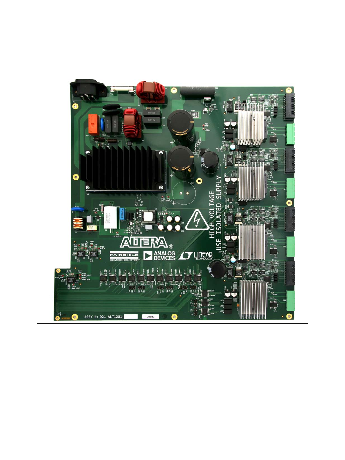
Figure 1 shows the Multiaxis Motor Control Board.
Figure 1. Multiaxis Motor Control Board
Multiaxis Motor Control Board February 2014 Altera Corporation
Page 5
Functional Description Page 5
Isolated
22-V Supply
Low-Voltage
Logic Supplies
400-V
DC Link
Bootstrap
Circuit
IGBTs
x4 Channel
Encoder
Interface
Current and
Voltage
Sensing
Ballast/
Brake
Mains
Input
Digital I/O Isolators
HSMC
Motors
Encoders
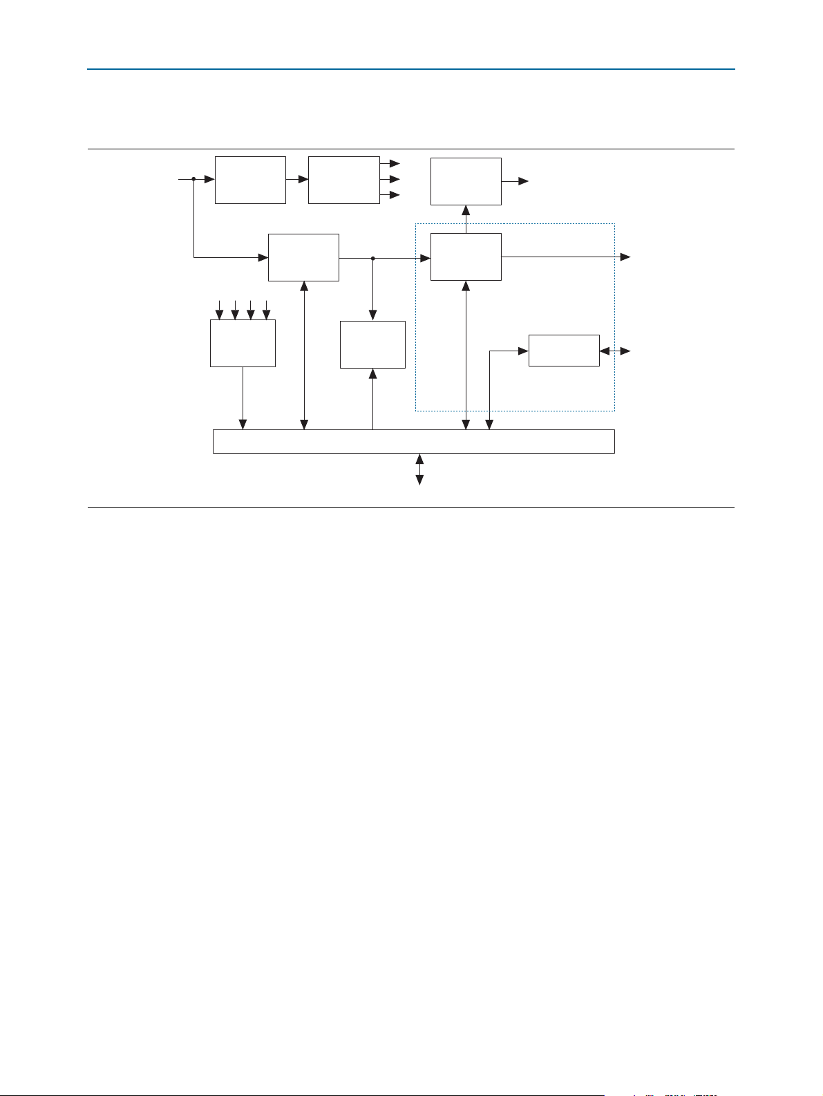
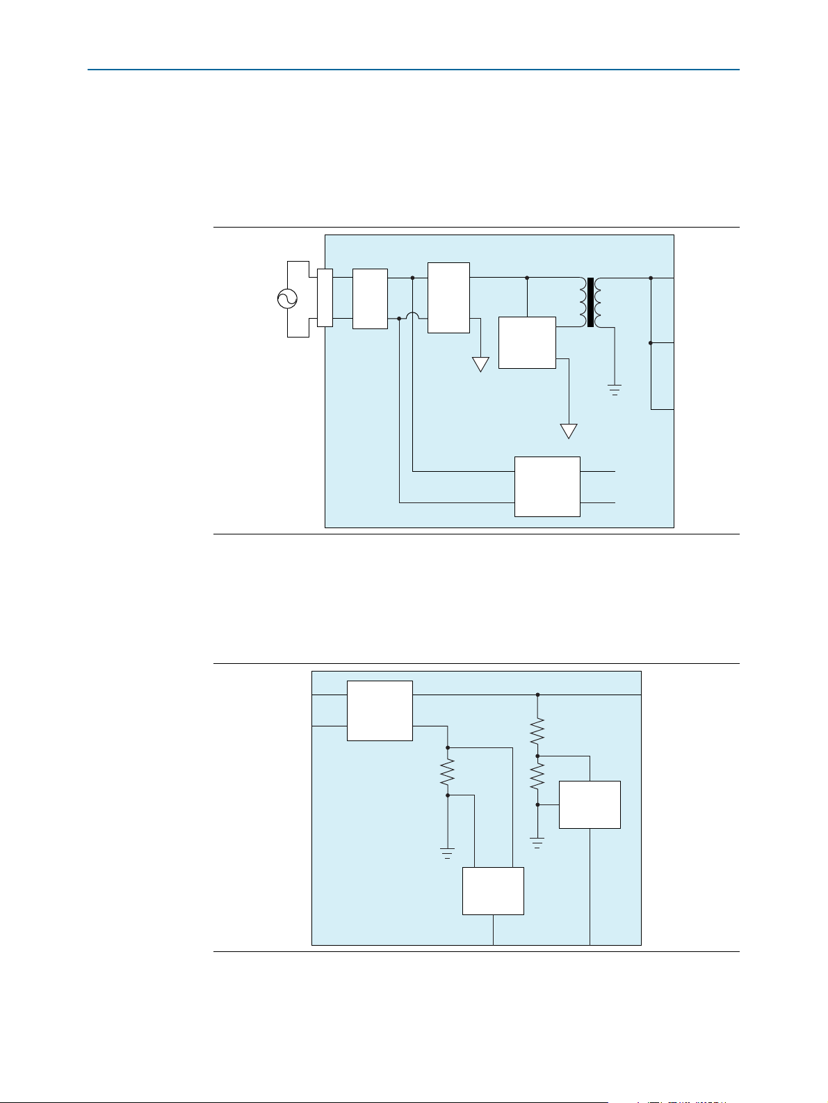
Figure 2 shows a high-level block diagram of the Multiaxis Motor Control Board.
Figure 2. Block Diagram
The following sections describe the functional blocks.
Digital I/O Isolators
Analog Devices ADuM1401 digital isolators isolate all digital I/O signals on the
Multiaxis Motor Control Board. They provide complete electrical isolation between
the host FPGA board and the power electronics on the Multiaxis Motor Control
Board. In some circuit locations, the board uses Silicon Labs Si8440 or Si8441 digital
isolators for their output behavior during power down, to prevent transient control
signals on the IGBT drivers.
One side of each isolator connects to the HSMC connector and takes power from the
HSMC connector. The other side of each isolator takes power from an isolated power
supply on the Multiaxis Motor Control Board.
Power Supplies
The Multiaxis Motor Control Board converts mains input to the DC link and a number
of lower voltages for logic and interfacing.
Multiaxis Motor Control BoardFebruary 2014 Altera Corporation
Page 6
Page 6 Functional Description
PFC
Bus
Converter
EMI
Filter
~~+
_
400 V at 4 A
22 V at 1A
90 - 240 VAC
50/60 Hz
Emerson
400-V PFC
Module
Isolated
SD-ADC
20 MSPS
3.3 V
3.3 V
400 V at 4 A
Emerson
400-V PFC
Module
Isolated
SD-ADC
20 MSPS
Mains Input
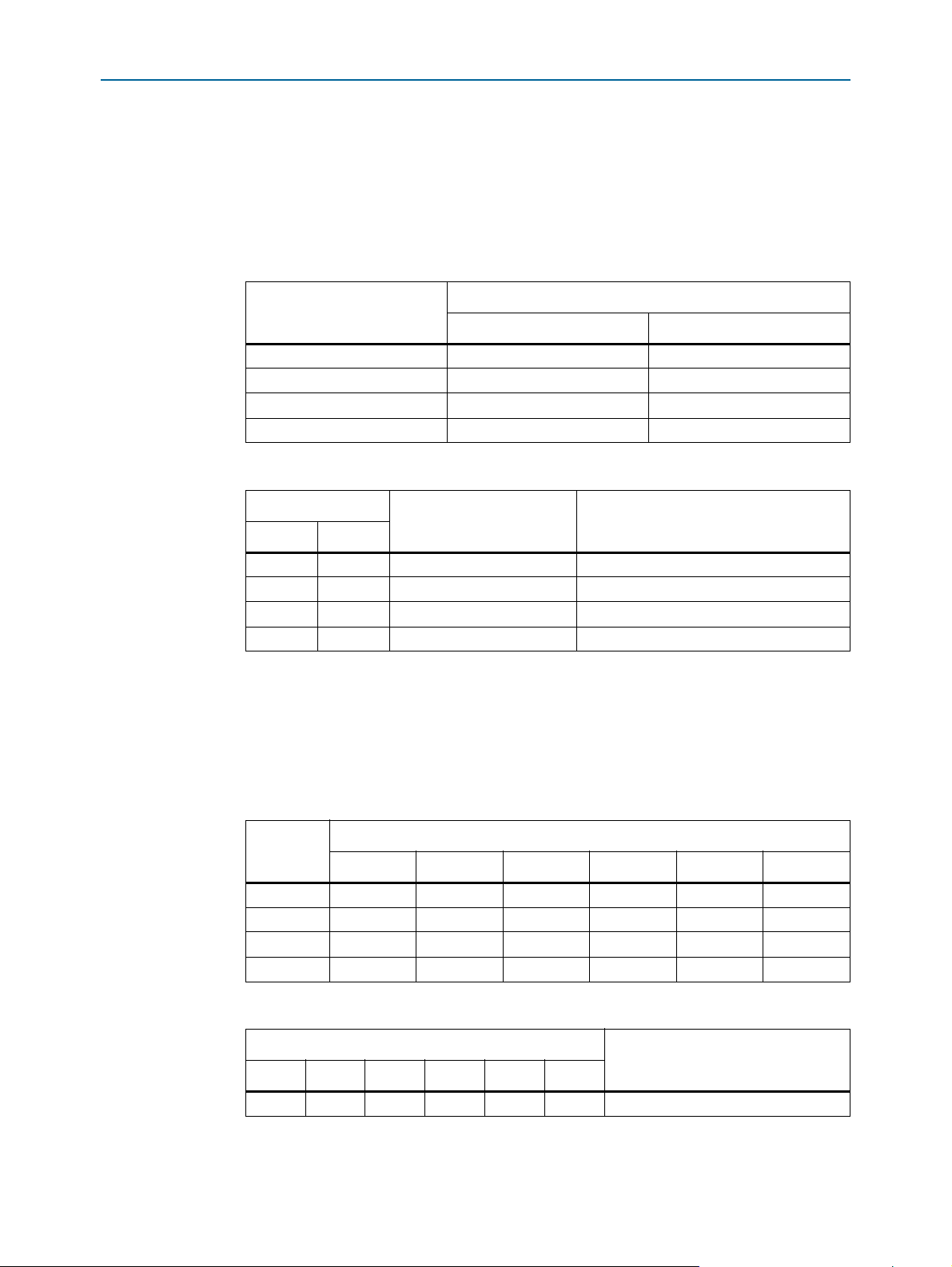
The Multiaxis Motor Control Board filters the mains input (Figure 3) and then splits to
the DC link and the 22-V power supply. Both power supplies incorporate PFC. The
Multiaxis Motor Control Board works with mains input voltages of 85 to 264 VAC, 50
or 60 Hz. The mains input includes an EMI filter.
Figure 3. Mains Input Filtering
DC Link and PFC
To provide unity power factor with very low-level harmonic distortion in line current,
an Emerson AIF04ZPFC-01L module produces the 400-V DC link voltage (Figure 4).
The PFC works over all typical line voltages used worldwide.
Figure 4. DC Link Voltage PFC Supply
Multiaxis Motor Control Board February 2014 Altera Corporation
Page 7

Functional Description Page 7
The DC link can supply up to 1.5 kW in total, across all four motor channels with a
mains input of 240 V. At lower mains voltages, the Multiaxis Motor Control Board
reduces the maximum power. For example, 1 kW at 110 V input. Isolated sigma-delta
ADCs allow you to monitor the DC link voltage and current.
Isolated 22 V Supply
A Linear Technology LT3798 provides an isolated 22-V supply that feeds further
switch mode regulators to generate all of the required voltages on the Multiaxis Motor
Control Board.
15 V IGBT Gate Drive Supply
Two Linear Technology LTC3631EDD#PBF generate the 15-V supplies that the IGBT
modules require. One LTC361 supplies motor channels 0 and 1; the other one supplies
motor channels 2 and 3.
3.3 V and 5 V Logic Supplies
The 3.3-V and 5-V supplies for logic devices both use Linear Technology LTM8022
DC/DC micromodules.
Brake
3.3 V Isolator Supply
The isolators connected to the HSMC connector can receive power directly from the
HSMC 3.3-V pins or from the HSMC 12-V pin via a Linear Technology LTM8022
micromodule switch mode power supply.
Encoder Power Supplies
Each motor channel includes a power supply (LTM8025 micromodule) for the
encoder interface that you can configure for 3.3 V, 5 V, or 12 V as required by the
encoder.
The Multiaxis Motor Control Board includes incorporates a brake circuit with a
Fairchild FAN3111E gate driver, Fairchild FGP15N60 IGBT, and 100-Ohm brake
resistor.
During braking, the kinetic energy of the motor feeds back into the DC link circuit as
extra stored energy in the DC link capacitor. You can turn on the brake resistor to
dissipate excess energy and prevent the DC link voltage from rising too high.
The peak power dissipation in the brake resistor is:
2
V
/R = V
As the brake resistor is rated for only 20 W continuous power dissipation, only use it
for only a few milliseconds. The gate drive to the brake circuit is AC coupled.The
FPGA must drive a square wave on the
A steady signal, either high or low, results in the Power Supply turning off the brake.
Furthermore, the FPGA should implement some form of time out to prevent you from
activating the brake for too long.
DCLINK
2
/100 = 1.6 kW
HSMC_MOTOR_BRAKE
signal to activate the brake.
Multiaxis Motor Control BoardFebruary 2014 Altera Corporation
Page 8

Page 8 Functional Description
The time constant of the AC coupling allows the brake resistor to be active for no
more than 1 ms if the
HSMC_MOTOR_BRAKE
signal remains asserted.
IGBTs
The Multiaxis Motor Control Board uses Fairchild FNB41560/B2 600V/15A smart
power modules for each of the four motor channels (Figure 5). These modules are
three-phase IGBT inverter bridges including control ICs for gate driving and
protection.
Murata MEE1S2415SC isolated DC/DC converters generate floating bootstrap
supplies for the gate drivers from the 15V supply. The bootstrap voltages also power
the ADCs that sample the motor current, via simple zener diode regulators.
The Multiaxis Motor Control Board uses software to ensure that the low side IGBT
activates long enough to produce the correct bootstrap voltage (refer to the Fairchild
AN-9070 Smart Power Module Motion-SPM Products Application Note). The bootstrap
capacitor for each channel on the Multiaxis Motor Control Board is 22 F.
Figure 5. IGBTs
Sigma-Delta Modulator ADCs
The Multiaxis Motor Control Board includes multiple Analog Devices AD7401
differential input sigma-delta modulators, each clocked at 20 MHz to monitor and
measure key voltage, current, and resolver output quantities. The Multiaxis Motor
Control Board uses isolated ADCs except the resolver encoder feedback conversion.
The Multiaxis Motor Control Board demodulates the bit streams from the ADCs in the
FPGA on the host board. The Multiaxis Motor Control Board isolates the digital
encoded data at the HSMC connector.
3-Phase
IGBT Inverter
500 W
Isolated
SD-ADC
20 MSPS
Isolated
SD-ADC
20 MSPS
Isolated
SD-ADC
20 MSPS
3.3 V
Multiaxis Motor Control Board February 2014 Altera Corporation
Page 9

Functional Description Page 9
DC Link Monitor
The Multiaxis Motor Control Board measures the DC Link voltage, V
sensing the voltage across a resistor divider chain representing:
DCLINK,
by
82/199682 * V
DCLINK
For example, a voltage of 41 mV corresponds to a DC link voltage of 100 V. The
sigma-delta modulated reading is available on the HSMC connector
HSMC_ADC_400V_PFC_V_DATA
signal.
After filtering in the FPGA, the Multiaxis Motor Control Board calculates the DC link
voltage, according to the equation:
DC link voltage (V) = ADC value × 0.048
The reference design software uses an equivalent formula based on integer arithmetic.
The Multiaxis Motor Control Board measures the ground return current of the PFC by
sensing the voltage across a 0.01 Ohm resistor in the ground return path. The sigmadelta modulated reading is available on the HSMC connector
HSMC_ADC_400V_PFC_I_DATA
signal.
After filtering in the FPGA, the Multiaxis Motor Control Board calculates the the DC
link return current, according to the equation:
DC Link return current (mA) = ADC value × 1.95
The reference design software uses an equivalent formula based on integer arithmetic.
IGBT Return Current
The Multiaxis Motor Control Board measures the ground return currents of the IGBT
modules by sensing the voltage across 0.05 Ohm resistors in the ground return paths.
The sigma-delta modulated readings are available on the HSMC connector
DRV_x_HSMC_MOTOR_RTN_DATA_OUT
signals.
After filtering in the FPGA, the Multiaxis Motor Control Board calculates the IGBT
return current according to the equation:
I (mA) = ADC value × 0.195
The drive on chip reference design software uses an equivalent formula based on
integer arithmetic.
Motor Phase Currents
Currents are measured in two of the three phases, U and W, by sensing the voltages
across 0.05 Ohm shunt resistors in series with the motor connections. The Vin+
terminals of the ADCs are connected nearest the motor. The Vin– terminals of the
ADCs are connected nearest the IGBT module.
After filtering in the FPGA, the Multiaxis Motor Control Board calculates motor phase
current according to the equation:
I (mA) = ADC value × 0.195
The reference design software uses an equivalent formula based on integer arithmetic.
The sigma-delta modulated readings are available on the HSMC connector
DRV_x_HSMC_U_DATA_OUT
and
DRV_x_HSMC_W_DATA_OUT
signals.
Multiaxis Motor Control BoardFebruary 2014 Altera Corporation
Page 10

Page 10 Functional Description
TI CDCLVC116
1:6 Buffers
Motor
Channel 0
ADCs
Total Current
& DC Link
ADCs
ADC
ADC Data
Feedback Clock
Isolator
HSMC
Connector
Motor
Channel 1
ADCs
Motor
Channel 2
ADCs
Motor
Channel 3
ADCs
The following equation calculates the current in the third, V, phase:
= –Iu –I
I
v
w
ADC Clock Tree
The 20-MHz ADC sample clock from the HSMC connector,
by a tree of CDCLVC1106 low-skew clock buffers (Figure 6).
To compensate for the isolator device propagation delays, the HSMC connector
provides a feedback clock,
CLK_HSMC_FEEDBACK
, to the FPGA. The Multiaxis Motor
Control Board compensates for the isolator propagation delays, but you must still
account for the part-to-part skew when creating I/O timing constraints for the FPGA
design.
Alternatively, you can use a PLL in the FPGA to create a phase shifted version of the
ADC clock for sampling the inputs.
Figure 6. Clock Tree
CLK_HSMC_ADC
, is buffered
Multiaxis Motor Control Board February 2014 Altera Corporation
Page 11

Functional Description Page 11
5 V
3.3 V3.3 V3.3 V
3.3 V3.3 V
3.3 V
3.3 V
5 V5 V
3.3 V
3.3 V
x2
x2
6
6
6
SE to Diff
SD-ADC
10 MSPS
RS-485
Transceiver
RS-485
Transceiver
Isolator
RS-485
Transceiver
Isolator Isolator Isolator Isolator
2
2
2
2
2
2
6
Resolver
SinCos
Quadrature/
Hall Effect
M
EnDAT
BiSS
Hiperface
EnDat, BiSS, and
HiperFace DSL
Encoder Interfaces
Resolver Sine and Cosine
Encoder Interface
Quadrature and Hall Effect
Encoder Interface
Tab le 4 lists the ADCs.
Table 4. ADCs
ADC Measured Quantity
DC-link monitor DC-link voltage 0.048
DC-link monitor DC-link current 1.95
IGBT return IGBT return current 0.195
Motor phase U Motor phase U current 0.195
Motor phase W Motor phase W current 0.195
Encoder Interfaces
Figure 7 shows the encoder interface.
Figure 7. Encoder Interface
Scaling
Factor
HSMC Signals
HSMC_ADC_400V_PFC_V_DATA
HSMC_ADC_400V_PFC_I_DATA
DRV_x_HSMC_MOTOR_RTN_DATA_OUT
DRV_x_HSMC_U_DATA_OUT
DRV_x_HSMC_W_DATA_OUT
Multiaxis Motor Control BoardFebruary 2014 Altera Corporation
Page 12

Page 12 Functional Description
VDD
DE
D
R
RE
NC1
NC2
Y
Z
A
B
NC3
GND1
GND2
+5 V
J5
J6
J7
J8
DRV_0_RS485_EN
DRV_0_RS485_TX
DRV_0_RS485_RX
+5 V
DRV_0_SER_DATA_TX_P
DRV_0_SER_DATA_TX_N
DRV_0_SER_DATA_RX_P
DRV_0_SER_DATA_RX_N
LTC1687CS
DNP
330 pF
200 V
DNP
330 pF
200 V
56 R
56 R
4K7
16 V
0.1 µF
16 V
2.2 µF
EnDat, BiSS, HIPERFACE DSL Encoder Interface
The Multiaxis Motor Control Board supports connection of encoders with RS485
interfaces. You may configure each motor channel independently for any of the
encoder interface types.
Each encoder interface type requires you to implement the appropriate interface IP
cores in the FPGA on the host board. Altera partners provide appropriate IP cores
with the reference design.
The Multiaxis Motor Control Board includes different electrical termination schemes
for the encoder interfaces. Figure 8 shows an example a channel (channel 0) interface
termination. Capacitors C107 and C111 are not fitted, Resistors R103, R106 and
capacitor C109 are fitted. The jumpers allow for independent pairs for TX and RX or
one common pair. Refer to Tab le 11 for other channel jumper settings.
Figure 8. Encoder Interface Termination
Multiaxis Motor Control Board February 2014 Altera Corporation
Resolver Sine and Cosine Encoder Interface
The FPGA on the host board implements IP cores to drive the single-ended resolver
stimulus signal with a sigma-delta encoded 8-kHz sine wave. The Multiaxis Motor
Control Board converts and filters this signal to a differential drive for the resolver.
ADS1205 dual channel 10-MHz sigma-delta ADCs, with a ±2.5-V input range, clocked
at 20 MHz, digitize resolver encoder sine and cosine feedback signals. The ADS1205
divides the applied clock internally to generate the 10-Mbps data rate. The Multiaxis
Motor Control Board passes the resulting bitstreams through isolators for isolation.
Page 13

Functional Description Page 13
Quadrature and Hall Effect Encoder Interface
The Multiaxis Motor Control Board allows you to connect two- and three-channel
quadrature encoders with RS485 interfaces.
IP cores in the FPGA on the host board decode the encoder signals.
HSMC Connector
The HSMC connector allows you to connect the Multiaxis Motor Control Board to an
FPGA host board.
f For more information on the HSMC connector, refer to the High Speed Mezzanine Card
(HSMC) Specification.
Tab le 5 lists the pin assignments for the HSMC connector. I/O direction is relative to
the Multiaxis Motor Control Board: input indicates input to the Multiaxis Motor
Control Board from the host board; output indicates an output signal from the
Multiaxis Motor Control Board to the host board.
Table 5. HSMC Connector Pin Assignments
Pin Signal Direction Function
1 to 38 — — Not used.
39
40
41
42
43
44
45 3.3 V — Power.
46 12 V — Power.
47
48
49
50
51 3.3 V — Power.
52 12 V — Power.
53
54
55
56
57 3.3 V — Power.
58 12 V — Power.
59
60
CLK_HSMC_ADC
CLK_HSMC_FEEDBACK
400V_PFC_PFW
DRV_0_HSMC_DRV_WH
400V_PFC_LD_EN
DRV_0_HSMC_DRV_VH
HSMC_MOTOR_BRAKE
DRV_0_HSMC_DRV_UH
400V_PFC_PF_EN
DRV_0_HSMC_W_DATA_OUT
HSMC_ADC_400V_PFC_I_DATA
DRV_0_HSMC_MOTOR_RTN_DATA_OUT
HSMC_ADC_400V_PFC_V_DATA
DRV_0_HSMC_U_DATA_OUT
DRV_0_HSMC_RS485_TX
DRV_0_HSMC_RSLVR_DRV_HALL_QUAD_A
Input Clock input for sigma-delta ADCs.
Output
Output PFC power fail warning.
Input Channel 0 phase W high side.
Output PFC load enable.
Input Channel 0 phase V high side.
Input Brake (chopper) enable.
Input Channel 0 phase U high side.
Input PFC enable.
Output Channel 0 phase W ADC data.
Output PFC return current ADC data.
Output Channel 0 IGBT return current ADC data.
Output PFC voltage ADC data.
Output Channel 0 phase U ADC data.
Input Channel 0 RS485 encoder TX data.
Input/Output Encoder dependent.
Feedback clock compensating for isolator
delays.
Multiaxis Motor Control BoardFebruary 2014 Altera Corporation
Page 14

Page 14 Functional Description
Table 5. HSMC Connector Pin Assignments
Pin Signal Direction Function
61
62
DRV_0_HSMC_RS485_EN
DRV_0_HSMC_RSLVR_COS_HALL_QUAD_B
Input Channel 0 RS485 encoder TX enable.
Output Encoder dependent.
63 3.3 V — Power.
64 12 V — Power.
65
66
67
68
CLK_DRV_0_HSMC_SER
DRV_0_HSMC_RSLVR_SIN_HALL_QUAD_C
DRV_0_HSMC_RS485_RX
DRV_0_HSMC_MOTOR_DRV_FAULT
Input Channel 0 encoder clock.
Output Encoder dependent.
Output Channel 0 RS485 encoder RX data.
Output Channel 0 IGBT fault status.
69 3.3 V — Power.
70 12 V — Power.
71
72
73
74
DRV_1_HSMC_RS485_TX
DRV_0_HSMC_DRV_WL
DRV_1_HSMC_RS485_EN
DRV_0_HSMC_DRV_VL
Input Channel 1 RS485 encoder TX data.
Input Channel 0 phase W low side.
Input Channel 0 RS485 encoder TX enable.
Input Channel 0 phase V low side.
75 3.3 V — Power.
76 12 V — Power.
77
78
79
80
CLK_DRV_1_HSMC_SER
DRV_0_HSMC_DRV_UL
DRV_1_HSMC_RS485_RX
DRV_1_HSMC_W_DATA_OUT
Input Channel 1 encoder clock.
Input Channel 0 phase U low side.
Output Channel 1 RS485 encoder RX data.
Output Channel 1 phase W ADC data.
81 3.3 V — Power.
82 12 V — Power.
83
84
85
86
DRV_1_HSMC_RSLVR_COS_HALL_QUAD_B
DRV_1_HSMC_MOTOR_RTN_DATA_OUT
DRV_1_HSMC_RSLVR_DRV_HALL_QUAD_A
DRV_1_HSMC_U_DATA_OUT
Output Encoder dependent.
Output Channel 1 IGBT return current ADC data.
Input/Output Encoder dependent..
Output Channel 1 phase U ADC data.
87 3.3 V — Power.
88 12 V — Power.
89
90
91
92
DRV_2_HSMC_RS485_EN
DRV_1_HSMC_MOTOR_DRV_FAULT
DRV_1_HSMC_RSLVR_SIN_HALL_QUAD_C
DRV_1_HSMC_DRV_WL
Input Channel 1 RS485 encoder TX enable.
Output Channel 1 IGBT fault status.
Output Encoder dependent.
Input Channel 1 phase W low side.
93 3.3 V — Power.
94 12 V — Power.
95
96
97
98
DRV_2_HSMC_RS485_TX
CLK_DRV_0_HSMC_ADC_OUT
DRV_2_HSMC_RS485_RX
CLK_DRV_1_HSMC_ADC_OUT
Input Channel 2 RS485 encoder TX data.
Output Channel 0 Resolver ADC output clock.
Output Channel 2 RS485 encoder RX data.
Output Channel 1 resolver ADC output clock.
99 3.3 V — Power.
Multiaxis Motor Control Board February 2014 Altera Corporation
Page 15

Functional Description Page 15
Table 5. HSMC Connector Pin Assignments
Pin Signal Direction Function
100 12 V — Power.
101
102
103
104
DRV_2_HSMC_U_DATA_OUT
DRV_1_HSMC_DRV_VL
DRV_2_HSMC_MOTOR_RTN_DATA_OUT
DRV_1_HSMC_DRV_UL
Output Channel 2 phase U ADC data.
Input Channel 1 phase V low side.
Output Channel 2 IGBT return current ADC data.
Input Channel 1 phase U low side.
105 3.3 V — Power.
106 12 V — Power.
107
108
109
110
CLK_DRV_2_HSMC_SER
DRV_1_HSMC_DRV_WH
DRV_2_HSMC_W_DATA_OUT
DRV_1_HSMC_DRV_VH
Input Channel 2 encoder clock.
Input Channel 1 phase W high side.
Output Channel 2 phase W ADC data.
Input Channel 1 phase V high side.
111 3.3 V — Power.
112 12 V — Power.
113
114
115
116
DRV_2_HSMC_RSLVR_COS_HALL_QUAD_B
DRV_1_HSMC_DRV_UH
DRV_2_HSMC_RSLVR_DRV_HALL_QUAD_A
DRV_3_HSMC_RS485_RX
Output Encoder dependent.
Input Channel 1 phase U high side.
Input/Output Encoder dependent.
Output Channel 3 RS485 encoder RX data.
117 3.3 V — Power.
118 12 V — Power.
119
120
121
122
DRV_2_HSMC_DRV_WH
DRV_3_HSMC_RS485_TX
DRV_2_HSMC_RSLVR_SIN_HALL_QUAD_C
DRV_3_HSMC_RS485_EN
Input Channel 2 phase W high side.
Input Channel 3 RS485 encoder TX data.
Output Encoder dependent.
Input Channel 3 RS485 encoder TX enable.
123 3.3 V — Power.
124 12 V — Power.
125
126
127
128
DRV_2_HSMC_DRV_UH
DRV_3_HSMC_RSLVR_SIN_HALL_QUAD_C
DRV_2_HSMC_DRV_VH
DRV_3_HSMC_RSLVR_COS_HALL_QUAD_B
Input Channel 2 phase U high side.
Output Encoder dependent.
Input Channel 2 phase V high side.
Output Encoder dependent.
129 3.3 V — Power.
130 12 V — Power.
131
132
133
134
DRV_2_HSMC_DRV_WL
DRV_3_HSMC_RSLVR_DRV_HALL_QUAD_A
DRV_2_HSMC_MOTOR_DRV_FAULT
DRV_3_HSMC_MOTOR_DRV_FAULT
Input Channel 2 phase W low side.
Input/Output Encoder dependent.
Output Channel 2 IGBT fault status.
Output Channel 3 IGBT fault status.
135 3.3 V — Power.
136 12 V — Power.
137
138
DRV_2_HSMC_DRV_UL
DRV_3_HSMC_DRV_WL
Input Channel 2 phase U low side.
Input Channel 3 phase W low side.
Multiaxis Motor Control BoardFebruary 2014 Altera Corporation
Page 16

Page 16 Functional Description
Table 5. HSMC Connector Pin Assignments
Pin Signal Direction Function
139
140
141 3.3 V — Power.
142 12 V — Power.
143
144
145
146
147 3.3 V — Power.
148 12 V — Power.
149
150
151
152
153 3.3 V — Power.
154 12 V — Power.
155 — — Not used.
156
157 — — Not used.
158
159 3.3 V — Power.
160
161 to
172
DRV_2_HSMC_DRV_VL
DRV_3_HSMC_DRV_VL
DRV_3_HSMC_DRV_VH
DRV_3_HSMC_DRV_UL
DRV_3_HSMC_DRV_UH
DRV_3_HSMC_W_DATA_OUT
CLK_DRV_3_HSMC_SER
DRV_3_HSMC_MOTOR_RTN_DATA_OUT
DRV_3_HSMC_DRV_WH
DRV_3_HSMC_U_DATA_OUT
CLK_DRV_2_HSMC_ADC_OUT
CLK_DRV_3_HSMC_ADC_OUT
PSNTn
0 V — Ground.
Input Channel 2 phase V low side.
Input Channel 3 phase V low side.
Input Channel 3 phase V high side.
Input Channel 3 phase U low side.
Input Channel 3 phase U high side.
Output Channel 3 phase W ADC data.
Input Channel 3 encoder clock.
Output Channel 3 IGBT return current ADC data.
Input Channel 3 phase W high side.
Output Channel 3 phase U ADC data.
Output Channel 2 resolver ADC output clock.
Output Channel 3 Resolver ADC output clock.
Input Presence.
Mains Input Fuse
A fuse, replacement part number LittleFuse 0324015 250V AC 15A, or equivalent
protects the mains input.
Motor Connectors
Tab le 6 lists the pin assignments for each channel.
Table 6. Motor Connector Pin Assignments
Pin Signal
1 Earth ground.
2 Motor phase U.
3 Motor phase V.
4 Motor phase W.
Multiaxis Motor Control Board February 2014 Altera Corporation
Page 17

Functional Description Page 17
Encoder Connectors
Tab le 7 lists the pin assignments for each channel. Not every encoder type requires all
connections to be made.
You may link the TX and RX pairs on pins 16, 17 and 18, 19 by jumpers on the
Multiaxis Motor Control Board to create a single bidirectional data pair.
Table 7. Encoder Connector Pin Assignments
Pin Signal I/O Encoder Type(s) SIgnal
1 Supply — — —
2
3
4
5
6
7
8
9
10
11
12
13
14
15
16
17
18
19
20 Ground — — —
DRV_x_SIN_DRV_P
DRV_x_SIN_DRV_N
DRV_x_RESOLVER_COS_N
DRV_x_RESOLVER_COS_P
DRV_x_RESOLVER_SIN_N
DRV_x_RESOLVER_SIN_P
DRV_x_HALL_QUAD_A_P
DRV_x_HALL_QUAD_A_N
DRV_x_HALL_QUAD_B_P
DRV_x_HALL_QUAD_B_N
DRV_x_HALL_QUAD_C_P
DRV_x_HALL_QUAD_C_N
CLK_DRV_x_SER_P
CLK_DRV_x_SER_N
DRV_x_SER_DATA_TX_P
DRV_x_SER_DATA_TX_N
DRV_x_SER_DATA_RX_P
DRV_x_SER_DATA_RX_N
O Resolver Stimulus+
O Resolver Stimulus–
I Resolver Cosine- signal
I Resolver Cosine+ signal
I Resolver Sine- signal
I Resolver Sine+ signal
I Hall, Quadrature Channel A+
I Hall, Quadrature Channel A–
I Hall, Quadrature Channel B+
I Hall, Quadrature Channel B–
I Hall, Quadrature Channel C+
I Hall, Quadrature Channel C–
O EnDat/BiSS/HIPERFACE Clock+
O EnDat/BiSS/HIPERFACE Clock–
O EnDat/BiSS/HIPERFACE TX+ data
O EnDat/BiSS/HIPERFACE TX– data
I EnDat/BiSS/HIPERFACE RX+ data
I EnDat/BiSS/HIPERFACE RX– data
Jumper Settings
Tab le 8 lists the jumpers.
Table 8. Jumpers
Jumper Function
J3 Channel 0 encoder power supply.
J4 Channel 0 encoder power supply.
J5 Channel 0 encoder RS485 data configuration.
J6 Channel 0 encoder RS485 data configuration.
J7 Channel 0 encoder RS485 data configuration.
J8 Channel 0 encoder RS485 data configuration.
J10 Channel 0 encoder interface selection.
Multiaxis Motor Control BoardFebruary 2014 Altera Corporation
Page 18

Page 18 Functional Description
Table 8. Jumpers
Jumper Function
J11 Channel 0 encoder interface selection.
J12 Channel 0 encoder interface selection.
J13 Channel 0 encoder interface selection.
J14 Channel 0 encoder interface selection.
J15 Channel 0 encoder interface selection.
J17 Channel 1 encoder power supply.
J18 Channel 1 encoder power supply.
J19 Channel 1 encoder RS485 data configuration.
J20 Channel 1 encoder RS485 data configuration.
J21 Channel 1 encoder RS485 data configuration.
J22 Channel 1 encoder RS485 data configuration.
J24 Channel 1 encoder interface selection.
J25 Channel 1 encoder interface selection.
J26 Channel 1 encoder interface selection.
J27 Channel 1 encoder interface selection.
J28 Channel 1 encoder interface selection.
J29 Channel 1 encoder interface selection.
J31 Channel 2 encoder power supply.
J32 Channel 2 encoder power supply.
J33 Channel 2 encoder RS485 data configuration.
J34 Channel 2 encoder RS485 data configuration.
J35 Channel 2 encoder RS485 data configuration.
J36 Channel 2 encoder RS485 data configuration.
J38 Channel 2 encoder interface selection.
J39 Channel 2 encoder interface selection.
J40 Channel 2 encoder interface selection.
J41 Channel 2 encoder interface selection.
J42 Channel 2 encoder interface selection.
J43 Channel 2 encoder interface selection.
J45 Channel 3 encoder power supply.
J46 Channel 3 encoder power supply.
J47 Channel 3 encoder RS485 data configuration.
J48 Channel 3 encoder RS485 data configuration.
J49 Channel 3 encoder RS485 data configuration.
J50 Channel 3 encoder RS485 data configuration.
J52 Channel 3 encoder interface selection.
J53 Channel 3 encoder interface selection.
J54 Channel 3 encoder interface selection.
J55 Channel 3 encoder interface selection.
Multiaxis Motor Control Board February 2014 Altera Corporation
Page 19

Functional Description Page 19
Table 8. Jumpers
Jumper Function
J56 Channel 3 encoder interface selection.
J57 Channel 3 encoder interface selection.
J58 3.3V isolated power supply.
Encoder Power Supply
The Multiaxis Motor Control Board can supply 3.3V, 5V or 12V encoder power supply
voltages. You may configure each channel's encoder power supply independently.
Tab le 9 lists the jumpers to set for each channel. Ta b le 1 0 lists the jumper positions for
encoder power supplies. Out means fit no jumper; in means fit a jumper.
Table 9. Jumpers for Encoder Power Supply
Channel
0J3J4
1 J17 J18
2 J31 J32
3 J45 J46
Table 10. Encoder Power Supply Selection
Jumper Position
Voltage (V) Encoder
AB
Out Out 12 EnDat
Out In 3.3 —
In Out 5 EnDat, BiSS
In In Invalid —
Jumpers
AB
Multiaxis Motor Control BoardFebruary 2014 Altera Corporation
Page 20
Page 20 Functional Description
Encoder RS485
For encoders that use an RS485 interface, configure the data pins for full-duplex
operation with combined TX and RX data or half-duplex operation with separate TX
and RX data. You may configure each channel independently. Ta ble 11 lists the
jumpers to set for each channel. Tabl e 12 lists the jumper positions for encoder RS485s.
Out means fit no jumper; in means fit a jumper.
Table 11. Jumpers for Each Channel for Encoder RS485 Data Configuration
Channel
AB
0 J5, J6 J7, J8
1 J19, J20 J21, J22
2 J33, J34 J35, J36
3 J47, J48 J49, J50
Table 12. Encoder RS485 Data Configuration
Jumper Position
Data Configuration Encoder
Ab
Out Out RX only. —
Out In Bidirectional on RX pair. EnDat
In Out Separate RX and TX. —
In In Bidirectional on TX pair. —
Jumpers
Encoder Interface
The Multiaxis Motor Control Board supports RS485, resolver, Hall effect and
quadrature encoders. You can configure each channel independently to support one
of these encoder standards at any one time. Tab le 1 3 lists the jumpers to set for each
channel. Ta bl e 1 4 lists the jumper positions for encoder interface selection.
Table 13. Jumpers for Each Channel for Encoder Selection
Channel
ABCDEF
0 J10 J11 J12 J13 J14 J15
1 J24 J25 J26 J27 J28 J29
2 J38 J39 J40 J41 J42 J43
3 J52 J53 J54 J55 J56 J57
Table 14. Encoder Interface Selection
Jumper Positions
ABCDEF
In In In Out Out Out Resolver.
Multiaxis Motor Control Board February 2014 Altera Corporation
Jumpers
Encoder Interface
Page 21

References Page 21
Table 14. Encoder Interface Selection
Jumper Positions
ABCDEF
Out Out Out In In In Hall effect, quadrature.
All other combinations Invalid.
The function of the three
DRV_x_HSMC_RSLVR_DRV_HALL_QUAD_y
Encoder Interface
signals on the HSMC
changes according to the jumper settings for resolver (Tab le 1 5) and Hall effect and
quadrature (Tab le 1 6).
Table 15. Resolver Interface Signals
Signal Direction Function
DRV_x_HSMC_RSLVR_DRV_HALL_QUAD_A
DRV_x_HSMC_RSLVR_COS_HALL_QUAD_B
DRV_x_HSMC_RSLVR_SIN_HALL_QUAD_C
Table 16. Hall Effect and Quadrature Signals
Signal Direction Function
DRV_x_HSMC_RSLVR_DRV_HALL_QUAD_A
DRV_x_HSMC_RSLVR_COS_HALL_QUAD_B
DRV_x_HSMC_RSLVR_SIN_HALL_QUAD_C
Input Resolver drive.
Output Resolver cosine ADC bitstream.
Output Resolver sine ADC bitstream.
Output Channel A.
Output Channel B.
Output Channel C.
HSMC Isolator Power Supply
References
You may source the power supply for the host FPGA board side of the isolators
directly from the HSMC 3.3-V supply or derive it from the HSMC 12-V supply by a
switching regulator module (Tab le 1 7). This feature allows for situations where
insufficient power is available from one or the other of the HSMC supplies.
Table 17. Isolator Isolated Power Supply
J58 Pins Linked Isolator 3.3V_ISO Power Supply
1 to 2 3.3-V auxiliary from HSMC 12 V via LTM8022 module.
2 to 3 Direct from HSMC 3/3 V.
■ Altera HSMC Specification
■ Altera Multiaxis Motor Control Board Schematics
■ Astec AIF – PFC 1600W AC-DC Converter Module Technical Reference Note
■ Fairchild FNB41560/B2 Smart Power Module Data Sheet
■ Fairchild AN-9070 Smart Power Module Motion-SPM Products Application Note
■ Analog Devices AD7401 Isolated Sigma-Delta Modulator Data Sheet
Multiaxis Motor Control BoardFebruary 2014 Altera Corporation
Page 22

Page 22 Document Revision History
■ Analog Devices ADS1205 Two 1-Bit, 10MHz, 2nd-Order, Delta-Sigma Modulator A-to-
D Converter Data Sheet
■ Analog Devices ADuM1401 Quad-Channel Digital Isola2014tors Data Sheet
■ Silicon Laboratories Si844x Digital Isolators Data Sheet
Document Revision History
Tab le 1 8 lists the revision history for this document.
Table 18. Document Revision History
Date Version Changes
February 2014 1.1 Replaced iCouplers with isolators.
August 2012 1.0 Initial release.
Multiaxis Motor Control Board February 2014 Altera Corporation
 Loading...