

Page 1

MAX V CPLD Development Board Reference Manual
MAX V CPLD Development Board
Reference Manual
101 Innovation Drive
San Jose, CA 95134
www.altera.com
MNL-01061-1.0
Subscribe
Page 2

© 2011 Altera Corporation. All rights reserved. ALTERA, ARRIA, CYCLONE, HARDCOPY, MAX, MEGACORE, NIOS, QUARTUS and STRATIX are Reg. U.S. Pat.
& Tm. Off. and/or trademarks of Altera Corporation in the U.S. and other countries. All other trademarks and service marks are the property of their respective
holders as described at www.altera.com/common/legal.html. Altera warrants performance of its semiconductor products to current specifications in accordance
with Altera’s standard warranty, but reserves the right to make changes to any products and services at any time without notice. Altera assumes no responsibility or
liability arising out of the application or use of any information, product, or service described herein except as expressly agreed to in writing by Altera. Altera
customers are advised to obtain the latest version of device specifications before relying on any published information and before placing orders for products or
services.
MAX V CPLD Development Board Reference Manual January 2011 Altera Corporation
Page 3

Contents
Chapter 1. Overview
Introduction . . . . . . . . . . . . . . . . . . . . . . . . . . . . . . . . . . . . . . . . . . . . . . . . . . . . . . . . . . . . . . . . . . . . . . . . . . . . 1–1
General Description . . . . . . . . . . . . . . . . . . . . . . . . . . . . . . . . . . . . . . . . . . . . . . . . . . . . . . . . . . . . . . . . . . . . . 1–1
Board Component Blocks . . . . . . . . . . . . . . . . . . . . . . . . . . . . . . . . . . . . . . . . . . . . . . . . . . . . . . . . . . . . . . . . . 1–1
Development Board Block Diagram . . . . . . . . . . . . . . . . . . . . . . . . . . . . . . . . . . . . . . . . . . . . . . . . . . . . . . . . 1–2
Handling the Board . . . . . . . . . . . . . . . . . . . . . . . . . . . . . . . . . . . . . . . . . . . . . . . . . . . . . . . . . . . . . . . . . . . . . . 1–2
Chapter 2. Board Components
Introduction . . . . . . . . . . . . . . . . . . . . . . . . . . . . . . . . . . . . . . . . . . . . . . . . . . . . . . . . . . . . . . . . . . . . . . . . . . . . 2–1
Board Overview . . . . . . . . . . . . . . . . . . . . . . . . . . . . . . . . . . . . . . . . . . . . . . . . . . . . . . . . . . . . . . . . . . . . . . . . . 2–2
Featured Device: MAX V CPLD . . . . . . . . . . . . . . . . . . . . . . . . . . . . . . . . . . . . . . . . . . . . . . . . . . . . . . . . . . . 2–3
I/O Resources . . . . . . . . . . . . . . . . . . . . . . . . . . . . . . . . . . . . . . . . . . . . . . . . . . . . . . . . . . . . . . . . . . . . . . . . 2–4
Configuration, Status, and Setup Elements . . . . . . . . . . . . . . . . . . . . . . . . . . . . . . . . . . . . . . . . . . . . . . . . . . 2–5
Configuration . . . . . . . . . . . . . . . . . . . . . . . . . . . . . . . . . . . . . . . . . . . . . . . . . . . . . . . . . . . . . . . . . . . . . . . . 2–5
CPLD Configuration over Embedded USB-Blaster . . . . . . . . . . . . . . . . . . . . . . . . . . . . . . . . . . . . . . 2–5
CPLD Configuration using External USB-Blaster . . . . . . . . . . . . . . . . . . . . . . . . . . . . . . . . . . . . . . . . 2–6
Status Elements . . . . . . . . . . . . . . . . . . . . . . . . . . . . . . . . . . . . . . . . . . . . . . . . . . . . . . . . . . . . . . . . . . . . . . . 2–6
Setup Elements . . . . . . . . . . . . . . . . . . . . . . . . . . . . . . . . . . . . . . . . . . . . . . . . . . . . . . . . . . . . . . . . . . . . . . . 2–7
Clock Circuitry . . . . . . . . . . . . . . . . . . . . . . . . . . . . . . . . . . . . . . . . . . . . . . . . . . . . . . . . . . . . . . . . . . . . . . . . . . 2–7
Connectors . . . . . . . . . . . . . . . . . . . . . . . . . . . . . . . . . . . . . . . . . . . . . . . . . . . . . . . . . . . . . . . . . . . . . . . . . . . . . 2–8
GPIO Headers . . . . . . . . . . . . . . . . . . . . . . . . . . . . . . . . . . . . . . . . . . . . . . . . . . . . . . . . . . . . . . . . . . . . . . . . 2–8
PC Speaker Header . . . . . . . . . . . . . . . . . . . . . . . . . . . . . . . . . . . . . . . . . . . . . . . . . . . . . . . . . . . . . . . . . . . 2–10
DC Motor Headers . . . . . . . . . . . . . . . . . . . . . . . . . . . . . . . . . . . . . . . . . . . . . . . . . . . . . . . . . . . . . . . . . . . 2–11
General User Input/Output . . . . . . . . . . . . . . . . . . . . . . . . . . . . . . . . . . . . . . . . . . . . . . . . . . . . . . . . . . . . . 2–13
User-Defined Push-Button Switches . . . . . . . . . . . . . . . . . . . . . . . . . . . . . . . . . . . . . . . . . . . . . . . . . . . . 2–13
User-Defined LEDs . . . . . . . . . . . . . . . . . . . . . . . . . . . . . . . . . . . . . . . . . . . . . . . . . . . . . . . . . . . . . . . . . . . 2–13
Off-Chip EEPROM . . . . . . . . . . . . . . . . . . . . . . . . . . . . . . . . . . . . . . . . . . . . . . . . . . . . . . . . . . . . . . . . . . . . . 2–14
2
I
C EEPROM . . . . . . . . . . . . . . . . . . . . . . . . . . . . . . . . . . . . . . . . . . . . . . . . . . . . . . . . . . . . . . . . . . . . . . . . 2–14
SPI EEPROM . . . . . . . . . . . . . . . . . . . . . . . . . . . . . . . . . . . . . . . . . . . . . . . . . . . . . . . . . . . . . . . . . . . . . . . . 2–15
Power Supply . . . . . . . . . . . . . . . . . . . . . . . . . . . . . . . . . . . . . . . . . . . . . . . . . . . . . . . . . . . . . . . . . . . . . . . . . . 2–16
Statement of China-RoHS Compliance . . . . . . . . . . . . . . . . . . . . . . . . . . . . . . . . . . . . . . . . . . . . . . . . . . . . 2–16
Additional Information
Document Revision History . . . . . . . . . . . . . . . . . . . . . . . . . . . . . . . . . . . . . . . . . . . . . . . . . . . . . . . . . . . Info–1
How to Contact Altera . . . . . . . . . . . . . . . . . . . . . . . . . . . . . . . . . . . . . . . . . . . . . . . . . . . . . . . . . . . . . . . . Info–1
Typographic Conventions . . . . . . . . . . . . . . . . . . . . . . . . . . . . . . . . . . . . . . . . . . . . . . . . . . . . . . . . . . . . . Info–2
January 2011 Altera Corporation MAX V CPLD Development Board Reference Manual
Page 4

iv Contents
MAX V CPLD Development Board Reference Manual January 2011 Altera Corporation
Page 5

Introduction
This document describes the hardware features of the MAX® V CPLD development
board, including the detailed pin-out and component reference information required
to create custom CPLD designs that interface with all components of the board.
General Description
The MAX V CPLD development board provides a hardware platform for developing
and prototyping low-cost, low-power CPLD designs, as well as to demonstrate the
features of the MAX V CPLD device.
To facilitate the development of MAX V CPLD designs, the board provides connectors
to interface to external functions or devices.
f For more information on the MAX V CPLD device family, refer to the MAX V Device
Handbook.
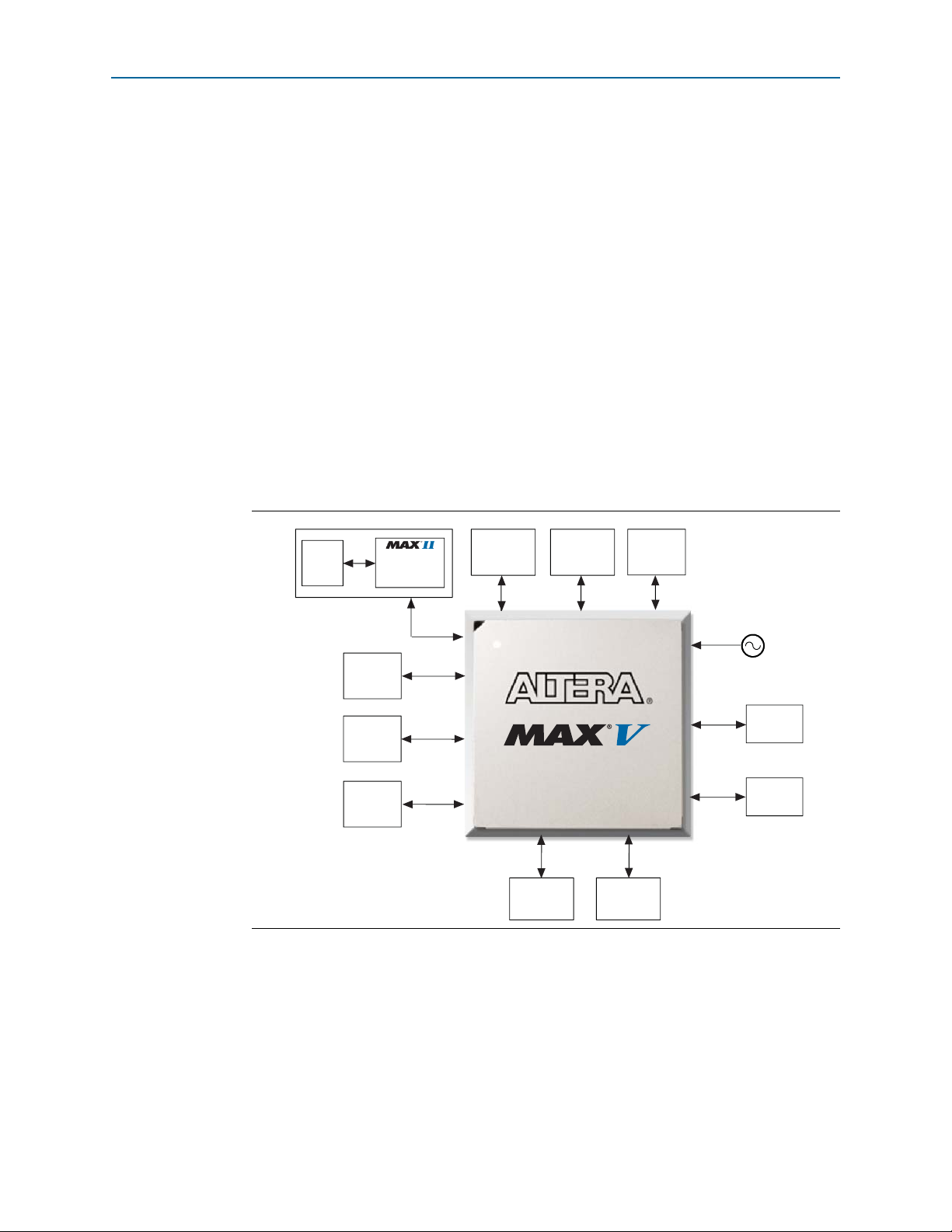
1. Overview
Board Component Blocks
The board features the following major component blocks:
■ MAX V CPLD 5M570ZF256C5N in a 256-pin FineLine BGA (FBGA) package
■ 570 logic elements (LEs)
■ 440 equivalent macrocells
■ 8,192-bits user flash memory (UFM)
■ 4 global clocks
■ 159 user I/Os
■ 1.8-V core power
■ MAX II EPM240M100C4N CPLD in the 100-pin Micro FBGA (MBGA) package
■ On-Board configuration circuitry
■ Embedded USB-Blaster
■ On-Board connectors
■ Type-B USB connector (as power source and communication port)
■ Two general purpose I/O (GPIO) 2×20-pin 0.1-inch expansion headers
■ One 4-pin PC speaker header
TM
for use with the Quartus® II Programmer
■ Two 2×3-pin DC motor headers
■ On-Board clocking circuitry
■ 10-MHz single-ended external oscillator
January 2011 Altera Corporation MAX V CPLD Development Board Reference Manual
Page 6
1–2 Chapter 1: Overview
DC Motor
Header 1
EPM240M100
Embedded
USB-Blaster
USB
2.0
x1
x9
x2
JTAG Chain
GPIO
Header 2
EP5M570ZF256N
SPI x4
User LEDs
Push-Button
Switches
x2
x36
I2C x2
10 MHz Oscillator
GPIO
Header 1
x36
PC Speaker
Header
Capacitor
Sense
Push-Button
Switch
x8
x9
DC Motor
Header 2
EEPROM
EEPROM
Development Board Block Diagram
■ General user I/O
■ LEDs and display
■ Two CPLD user LEDs
■ One USB status LED
■ One power status LED
■ Push-Button switches
■ Two user-defined push-button switches
■ One capacitor sense push-button switch
■ Mechanical
■ 4.1” × 3.1” board
Development Board Block Diagram
Figure 1–1 shows the block diagram of the MAX V CPLD development board.
Figure 1–1. MAX V CPLD Development Board Block Diagram
Handling the Board
When handling the board, it is important to observe the following static discharge
precaution:
c Without proper anti-static handling, the board can be damaged. Therefore, use
anti-static handling precautions when touching the board.
MAX V CPLD Development Board Reference Manual January 2011 Altera Corporation
Page 7

Introduction
1 A complete set of schematics, a physical layout database, and GERBER files for the
f For information about powering up the board and installing the demonstration
2. Board Components
This chapter introduces the major components on the MAX V CPLD development
board. Figure 2–1 illustrates major component locations and Table 2–1 provides a brief
description of all component features of the board.
development board reside in the MAX V CPLD development kit documents directory.
software, refer to the MAX V CPLD Development Kit User Guide.
This chapter consists of the following sections:
■ “Board Overview”
■ “Featured Device: MAX V CPLD” on page 2–3
■ “Configuration, Status, and Setup Elements” on page 2–5
■ “Clock Circuitry” on page 2–7
■ “Connectors” on page 2–8
■ “General User Input/Output” on page 2–13
■ “Off-Chip EEPROM” on page 2–14
■ “Power Supply” on page 2–16
■ “Statement of China-RoHS Compliance” on page 2–16
January 2011 Altera Corporation MAX V CPLD Development Board Reference Manual
Page 8
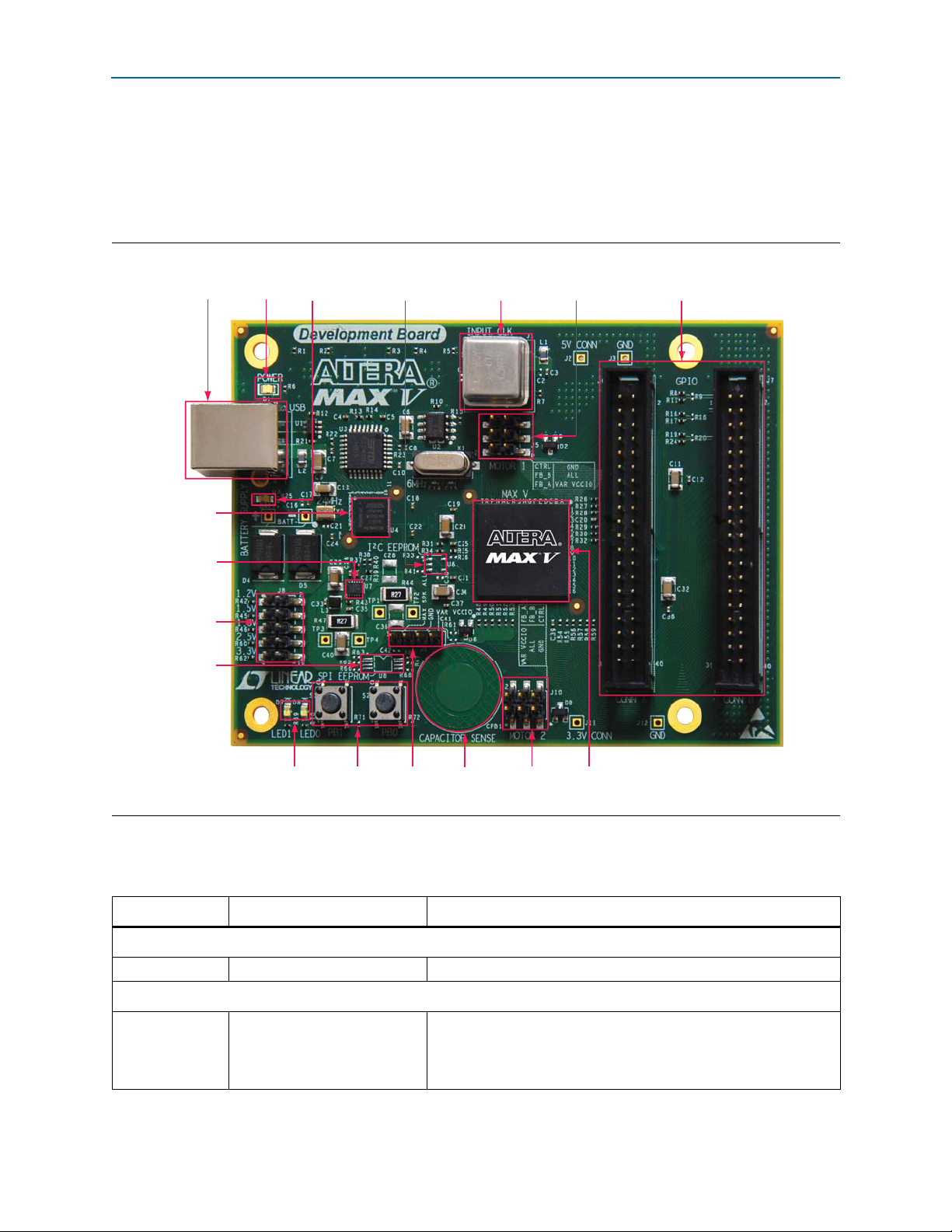
2–2 Chapter 2: Board Components
MAX V
CPLD
(U5)
10-MHz Single-Ended
External Oscillator
(J1)
User
LEDs
(D7, D8)
GPIO Headers
(J6, J7)
USB Type-B
Connector (J4)
Motor Control
Header 1
(J5)
Power LED
(D1)
User
Push-Button
Switches (S1, S2)
MAX II CPLD
EPM240M100C4N
(For embedded
USB-Blaster) (U4)
Motor Control
Header 2
(J10)
Speaker
Header
(J9)
Footprint for
I
2
C EEPROM
(U6)
Footprint for
SPI EEPROM
(U8)
Powe r
Regulator
(U7)
USB LED
(D3)
Capacitor
Sense Button
(CPB1)
VAR_VCCIO
Voltage Output
Selection Jumper
(U7)
Board Overview
Board Overview
This section provides an overview of the MAX V CPLD development board,
including an annotated board image and component descriptions. Figure 2–1
provides an overview of the development board features.
Figure 2–1. Overview of the MAX V CPLD Development Board Features
Tab le 2– 1 describes the components and lists their corresponding board references.
Table 2–1. MAX V CPLD Development Board Components (Part 1 of 2)
Board Reference Type Description
Featured Device
U5 CPLD MAX V 5M570ZF256C5N, 256-pin FBGA.
Configuration, Status, and Setup Elements
Connects the USB cable to the computer to enable embedded
J4 USB Type-B connector
USB-Blaster JTAG. The connector also supplies power to the board
through a USB cable when the cable is connected to a PC USB slot at
the other end.
MAX V CPLD Development Board Reference Manual January 2011 Altera Corporation
Page 9

Chapter 2: Board Components 2–3
Featured Device: MAX V CPLD
Table 2–1. MAX V CPLD Development Board Components (Part 2 of 2)
Board Reference Type Description
U3 USB 2.0 PHY
U4 CPLD MAX II CPLD EPM240M100.
J13, J14 JTAG header
D1 Power LED Illuminates when 5-V USB power is present.
D3 USB LED Illuminates to indicate USB-JTAG activity.
Clock Circuitry
J1 10-MHz oscillator 10-MHz single-ended input clock for the MAX V CPLD.
X1 6-MHz oscillator 6-MHz input clock for the FTDI USB 2.0 PHY device.
Y1 24-MHz oscillator 24-MHz input clock for the MAX II CPLD EPM240M100.
Connectors
J6, J7 GPIO headers Two general-purpose 2x40-pin 0.1-inch expansion headers.
J9 PC speaker header
J5, J10 DC motor headers Two motor headers which connects to the MAX V CPLD I/O bank 2.
A FTDI USB 2.0 PHY device to configure the CPLD over embedded
USB-Blaster.
Footprint (at the bottom of the board) to mount a JTAG header. The
header allows direct-access to devices in the JTAG connection.
A 4-pin PC speaker header which connects to the MAX V CPLD I/O
bank 2.
General User Input/Output
D7, D8 User LEDs Two user LEDs. Illuminates when driven low.
S1, S2 User push-button switches Two user push-button switches. Driven low when pressed.
CPB1 Capacitor sense button One capacitive touch-sense user-defined button.
Off-Chip EEPROM
U6 I
U8 SPI EEPROM Footprint to install a SPI EEPROM.
2
C EEPROM Footprint to install an I2C serial EEPROM
Featured Device: MAX V CPLD
The MAX V CPLD development board features the MAX V CPLD 5M570ZF256C5N
device (U5) in a 256-pin FBGA package.
Tab le 2– 2 describes the features of the MAX V CPLD 5M570ZF256C5N device.
Table 2–2. MAX V CPLD 5M570ZF256C5N Device Features
Equivalent LEs User Flash Memory (bits) User I/Os Global Clocks Package Type
570 8192 159 4 256-pin FBGA
f For more information about MAX V CPLD device family, refer to the MAX V Device
Handbook.
January 2011 Altera Corporation MAX V CPLD Development Board Reference Manual
Page 10

2–4 Chapter 2: Board Components
Featured Device: MAX V CPLD
Tab le 2– 3 lists the MAX V CPLD device component reference and manufacturing
information.
Table 2–3. MAX V CPLD Device Component Reference and Manufacturing Information
Board Reference Description Manufacturer
U5
MAX V CPLD, 256-pin FBGA
package, 570 LEs, lead-free.
Altera
Corporation 5M570ZF256C5N www.altera.com
I/O Resources
The 5M570ZF256C5N device support two I/O banks and each of these banks support
all t he LVT T L, LVC MO S, LVD S , a nd RS DS st a ndard s .
Figure 2–2 illustrates the bank organization for the 5M570ZF256C5N device in a
256-pin FBGA package.
Figure 2–2. 5M570ZF256C5N Device I/O Bank Diagram (Note 1)
I/O Bank 1
5M570ZF256C5N
Manufacturing
Part Number
Manufacturer
Website
I/O Bank 2
Note to Figure 2–2:
(1) This figure is a top view of the silicon die and is a graphical representation only. Refer to the pin list and the Quartus II
software for exact pin locations.
Tab le 2– 4 lists the MAX V CPLD device pin count and usage by function on the
development board.
Table 2–4. MAX V CPLD Device I/O Pin Count and Usage (Part 1 of 2)
Function I/O Standard I/O Count Special Pins
40-pin GPIO Header A 3.3-V CMOS 36 —
40-pin GPIO Header B
PC Speaker Header 8 —
1.2-V to 3.3-V
36 —
DC Motor Headers 18 —
MAX V CPLD Development Board Reference Manual January 2011 Altera Corporation
Page 11

Chapter 2: Board Components 2–5
Configuration, Status, and Setup Elements
Table 2–4. MAX V CPLD Device I/O Pin Count and Usage (Part 2 of 2)
Function I/O Standard I/O Count Special Pins
Push-Buttons
User LEDs 2 —
2
I
C EEPROM 2 —
SPI EEPROM 4 —
Clock 1 —
3.3-V CMOS
2 Push-button 2:
Dev_CLRn
Device I/O Total:
109/159
Configuration, Status, and Setup Elements
This section describes the board's configuration, status, and setup elements.
Configuration
The MAX V CPLD development board supports the following device configuration
methods:
■ Embedded USB-Blaster is the default method for configuring the CPLD at any
time using the Quartus II Programmer in JTAG mode with the supplied USB cable.
■ External USB-Blaster for configuring the CPLD using a JTAG connector. To use this
optional method to configure the CPLD, you have to mount the JTAG connector or
header to the back of the board.
CPLD Configuration over Embedded USB-Blaster
The USB-Blaster is implemented using a USB Type-B connector (J4), a FTDI USB 2.0
PHY device (U3), and an Altera MAX II CPLD EPM240M100 (U4). This allows the
configuration of the MAX V CPLD using a USB cable which connects between the
USB port on the board (J4) and a USB port of a PC running the Quartus II software.
The JTAG chain is normally mastered by the embedded USB-Blaster found in the
MAX
II CPLD EPM240M100.
January 2011 Altera Corporation MAX V CPLD Development Board Reference Manual
Page 12

2–6 Chapter 2: Board Components
Configuration, Status, and Setup Elements
Figure 2–3 illustrates an exmaple of the JTAG chain connection.
Figure 2–3. JTAG Chain
(Connector not mounted)
JTAG
2 x 5 Header
TDI
TDO
TMS
Embedded USB-Blaster
TCK
USB
PHY
MAX II
EPM240M100
GPIO (TCK)
GPIO (TMS)
GPIO (TDO)
GPIO (TDI)
TDI
TDO
TMS
TCK
TDI
TDO
TMS
TCK
JTAG
2 x 5 Header
(Connector not mounted)
MAX V CPLD
5M570ZF256C5N
TMS
TCK
TDI
TDO
The primary configuration mode for the MAX V CPLD is via JTAG using the MAX II
configuration controller design (embedded USB-Blaster). The board also includes a
JTAG connector which interfaces directly to the MAX V CPLD as the alternate source
for configuration.
CPLD Configuration using External USB-Blaster
The JTAG programming header (J13) provides another method for configuring the
CPLD using an external USB-Blaster device with the Quartus II Programmer running
on a PC. The external USB-Blaster connects to the board through the JTAG connector.
Figure 2–3 illustrates the JTAG chain.
Status Elements
This section describes the status elements. The development board includes two
status LEDs which connects to the MAX V CPLD.
Tab le 2– 5 lists the LED board references, names, and functional descriptions.
Table 2–5. Board-Specific LEDs
Board Reference LED Name Description
D1 Power Blue LED. Illuminates when power is active.
D3 USB
MAX V CPLD Development Board Reference Manual January 2011 Altera Corporation
Green LED. Illuminates when the embedded USB-Blaster is in use. Driven by the
MAX II CPLD EPM240M100.
Page 13

Chapter 2: Board Components 2–7
5M570ZF256C5N
Single-Ended
Clock
10 MHz
Clock Circuitry
Tab le 2– 6 lists the board-specific LEDs component references and manufacturing
information.
Table 2–6. Board-Specific LEDs Component References and Manufacturing Information
Board Reference Description Manufacturer Manufacturer Part Number Manufacturer Website
D1 Blue LED Lite-On LTST-C170TBKT www.liteon.com
D3 Green LEDs Lumex Inc. SML-LXT0805GW-TR www.lumex.com
Setup Elements
The development board does not have any setup elements.
1 To power-up the board, ensure that the
plugging the USB cable into the USB Type-B connector (J4).
Clock Circuitry
The development board includes a single-ended clock input on a 4-pin through-hole
socket. To replace the clock input with a different frequency oscillator, unplug the
current oscillator from the board and plug the desired oscillator into the 4-pin socket.
Figure 2–4 shows the MAX V CPLD development board clock input.
Figure 2–4. MAX V CPLD Development Board Clock Input
The development board also includes a 6-MHz crystal oscillator which provides the
input clock for the USB 2.0 PHY device.
VAR_VCCIO
jumper is set to 3.3 V before
Tab le 2– 16 lists the oscillator component reference and the manufacturing
information.
Table 2–7. Oscillator Component Reference and Manufacturing Information
Board
Reference
10-MHz oscillator, 3.3 V,
J1
X1
Y1
January 2011 Altera Corporation MAX V CPLD Development Board Reference Manual
CMOS, 12.7 mm × 12.7 mm,
1/2-SZ, ±30 ppm.
6-MHz crystal oscillator, 20pF
SMD.
24-MHz oscillator, 3.3 V,
CMOS SMD 3.2 mm × 2.5 mm,
±50 ppm.
Description Manufacturer
Abracon Corporation ACHL-10.000MHZ-EK www.abracon.com
CTS Corporation ATS060SM-T www.ctscorp.com
Abracon Corporation ASE-24.000MHZ-ET www.abracon.com
Manufacturer
Part Number
Manufacturer Website
Page 14

2–8 Chapter 2: Board Components
Connectors
Connectors
This section describes the connectors available on the development board.
GPIO Headers
There are two general-purpose 2×20-pin 0.1-inch expansion headers to allow the
addition of daughtercards for supplementary board features and functions.
Tab le 2– 15 lists the GPIO header A schematic signal names and their corresponding
MAX V CPLD device pin numbers.
Table 2–8. GPIO Header A Schematic Signal Names and Functions
Board Reference Description
J6.1 GPIO connector A pin
J6.2 GPIO connector A pin
J6.3 GPIO connector A pin
J6.4 GPIO connector A pin
J6.5 GPIO connector A pin
J6.6 GPIO connector A pin
J6.7 GPIO connector A pin
J6.8 GPIO connector A pin
J6.9 GPIO connector A pin
J6.10 GPIO connector A pin
J6.11 Power
J6.12 Ground
J6.13 GPIO connector A pin
J6.14 GPIO connector A pin
J6.15 GPIO connector A pin
J6.16 GPIO connector A pin
J6.17 GPIO connector A pin
J6.18 GPIO connector A pin
J6.19 GPIO connector A pin
J6.20 GPIO connector A pin
J6.21 GPIO connector A pin
J6.22 GPIO connector A pin
J6.23 GPIO connector A pin
J6.24 GPIO connector A pin
J6.25 GPIO connector A pin
J6.26 GPIO connector A pin
J6.27 GPIO connector A pin
J6.28 GPIO connector A pin
J6.29 Power
J6.30 Ground
Schematic Signal
Name
AGPIO_1
AGPIO_2
AGPIO_3
AGPIO_4
AGPIO_5
AGPIO_6
AGPIO_7
AGPIO_8
AGPIO_9
AGPIO_10
5VIN_CONN
GND
AGPIO_11
AGPIO_12
AGPIO_13
AGPIO_14
AGPIO_15
AGPIO_16
AGPIO_17
AGPIO_18
AGPIO_19
AGPIO_20
AGPIO_21
AGPIO_22
AGPIO_23
AGPIO_24
AGPIO_25
AGPIO_26
3.3VIN_CONN
GND
I/O Standard
3.3-V
5-V —
——
3.3-V
——
MAX V CPLD Device
Pin Number
P2
M4
L4
N3
N2
N1
M3
M2
M1
L3
L1
L2
K2
K3
J3
K1
J1
J2
H2
H3
G3
H1
G1
G2
F2
F3
—
MAX V CPLD Development Board Reference Manual January 2011 Altera Corporation
Page 15

Chapter 2: Board Components 2–9
Connectors
Table 2–8. GPIO Header A Schematic Signal Names and Functions
Board Reference Description
J6.31 GPIO connector A pin
J6.32 GPIO connector A pin
J6.33 GPIO connector A pin
J6.34 GPIO connector A pin
J6.35 GPIO connector A pin
J6.36 GPIO connector A pin
J6.37 GPIO connector A pin
J6.38 GPIO connector A pin
J6.39 GPIO connector A pin
J6.40 GPIO connector A pin
Schematic Signal
AGPIO_27
AGPIO_28
AGPIO_29
AGPIO_30
AGPIO_31
AGPIO_32
AGPIO_33
AGPIO_34
AGPIO_35
AGPIO_36
Tab le 2– 15 lists the GPIO header B schematic signal names and their corresponding
MAX V CPLD device pin numbers.
Table 2–9. GPIO Header B Schematic Signal Names and Functions
Board Reference Description
J7.1 GPIO connector B pin
J7.2 GPIO connector B pin
J7.3 GPIO connector B pin
J7.4 GPIO connector B pin
J7.5 GPIO connector B pin
J7.6 GPIO connector B pin
Schematic Signal
BGPIO_P_1_R
BGPIO_N_1_R
BGPIO_P_2_R
BGPIO_N_2_R
BGPIO_P_3_R
BGPIO_N_3_R
J7.7 GPIO connector B pin
J7.8 GPIO connector B pin
J7.9 GPIO connector B pin
J7.10 GPIO connector B pin
J7.11 Power
BGPIO_10
5VIN_CONN
J7.12 Ground
J7.13 GPIO connector B pin
J7.14 GPIO connector B pin
J7.15 GPIO connector B pin
J7.16 GPIO connector B pin
J7.17 GPIO connector B pin
J7.18 GPIO connector B pin
J7.19 GPIO connector B pin
J7.20 GPIO connector B pin
J7.21 GPIO connector B pin
J7.22 GPIO connector B pin
J7.23 GPIO connector B pin
BGPIO_11
BGPIO_12
BGPIO_13
BGPIO_14
BGPIO_15
BGPIO_16
BGPIO_17
BGPIO_18
BGPIO_19
BGPIO_20
BGPIO_21
Name
Name
BGPIO_7
BGPIO_8
BGPIO_9
GND
I/O Standard
3.3-V
I/O Standard
Variable VCCIO
voltage
(1.2-V to 3.3-V)
MAX V CPLD Device
Pin Number
E3
F1
E1
E2
D2
D3
C3
D1
E4
C2
MAX V CPLD Device
Pin Number
D15
C14
D16
C15
E15
D13
B14
C12
E16
E14
—
—
F13
F16
F15
F14
G16
G15
G14
H16
H15
H14
J16
January 2011 Altera Corporation MAX V CPLD Development Board Reference Manual
Page 16

2–10 Chapter 2: Board Components
Table 2–9. GPIO Header B Schematic Signal Names and Functions
Connectors
Board Reference Description
J7.24 GPIO connector B pin
J7.25 GPIO connector B pin
J7.26 GPIO connector B pin
J7.27 GPIO connector B pin
J7.28 GPIO connector B pin
J7.29 Power
J7.30 Ground
J7.31 GPIO connector B pin
J7.32 GPIO connector B pin
J7.33 GPIO connector B pin
J7.34 GPIO connector B pin
J7.35 GPIO connector B pin
J7.36 GPIO connector B pin
J7.37 GPIO connector B pin
J7.38 GPIO connector B pin
J7.39 GPIO connector B pin
J7.40 GPIO connector B pin
Schematic Signal
Name
BGPIO_22
BGPIO_23
BGPIO_24
BGPIO_25
BGPIO_26
3.3VIN_CONN
GND
BGPIO_27
BGPIO_28
BGPIO_29
BGPIO_30
BGPIO_31
BGPIO_32
BGPIO_33
BGPIO_34
BGPIO_35
BGPIO_36
I/O Standard
Variable VCCIO
voltage
(1.2-V to 3.3-V)
3.3-V —
——
Variable VCCIO
voltage
(1.2-V to 3.3-V)
MAX V CPLD Device
Pin Number
J15
J14
K16
K15
K14
L16
L15
L14
M16
M15
M14
L13
M13
N14
N13
Tab le 2– 16 lists the GPIO headers component reference and the manufacturing
information.
Table 2–10. GPIO Headers Component Reference and Manufacturing Information
Board Reference Description Manufacturer
J6, J7 GPIO headers JMSCONN Technology 217040SE www.jmsconn.com
Manufacturer
Part Number
Manufacturer Website
PC Speaker Header
The development board includes one PC speaker header which connects to the MAX
V CPLD I/O bank 2. The speaker header also supports a compatible standard
four-pin motherboard speaker.
MAX V CPLD Development Board Reference Manual January 2011 Altera Corporation
Page 17

Chapter 2: Board Components 2–11
Connectors
Tab le 2– 15 lists the speaker header schematic signal names and their corresponding
MAX V CPLD device pin numbers.
Table 2–11. Speaker Header Schematic Signal Names and Functions
Board Reference Description
Speaker header I/O pin
Speaker header I/O pin
Speaker header I/O pin
J9.1
Speaker header I/O pin
Speaker header I/O pin
Speaker header I/O pin
Speaker header I/O pin
Speaker header I/O pin
J9.4 Power
J9.3 Ground
Schematic Signal
Name
MAX_SPK_0
MAX_SPK_1
MAX_SPK_2
MAX_SPK_3
MAX_SPK_4
MAX_SPK_5
MAX_SPK_6
MAX_SPK_7
VAR_VCCIO
GND
I/O Standard
Variable VCCIO
voltage
(1.2-V to 3.3-V)
——
MAX V CPLD Device
Pin Number
N15
N16
P15
P14
H12
J12
A8
A7
—
Tab le 2– 16 lists the speaker header component reference and the manufacturing
information.
Table 2–12. Speaker Header Component Reference and Manufacturing Information
Board Reference Description Manufacturer
J9
—
Note to Table 2–12:
(1) This component is a compatible unit which can be used on the development board. The MAX V CPLD development kit does not include this
component.
0.025 inches (0.64 mm) square
post header
4-pin, 2-wire motherboard
speaker (1)
Samtec TSW-104-07-G-S www.samtec.com
Pc Parts
Collection
Manufacturer
Part Number
Manufacturer Website
20503 www.pcpartscollection.com
DC Motor Headers
The development board includes two DC motor headers which are driven by six
open-drain I/Os from the MAX V CPLD. The headers can directly drive micro DC
motor and also provides two channels for DC motor encoder to measure the motor’s
rotation speed.
January 2011 Altera Corporation MAX V CPLD Development Board Reference Manual
Page 18

2–12 Chapter 2: Board Components
Connectors
Tab le 2– 15 lists the motor headers schematic signal names and their corresponding
MAX V CPLD device pin numbers.
Table 2–13. Motor Headers Schematic Signal Names and Functions
Board Reference Description
Motor header 1 I/O pin
Motor header 1 I/O pin
J5.3
Motor header 1 I/O pin
Motor header 1 I/O pin
Motor header 1 I/O pin
Motor header 1 I/O pin
J5.2 Motor header 1 feedback signal A
J5.4 Motor header 1 feedback signal B
J5.6 Motor header 1 control signal
J5.1 Power
J5.5 Ground
Motor header 2 I/O pin
Motor header 2 I/O pin
J10.3
Motor header 2 I/O pin
Motor header 2 I/O pin
Motor header 2 I/O pin
Motor header 2 I/O pin
J10.2 Motor header 2 feedback signal A
J10.4 Motor header 2 feedback signal B
J10.6 Motor header 2 control signal
J10.1 Power
J10.5 Ground
Schematic Signal
Name
MAX_MOTOR_1_0
MAX_MOTOR_1_1
MAX_MOTOR_1_2
MAX_MOTOR_1_3
MAX_MOTOR_1_4
MAX_MOTOR_1_5
MOTOR_1_FB_A
MOTOR_1_FB_B
MOTOR_1_FB_CTRL
VAR_VCCIO
GND
MAX_MOTOR_2_0
MAX_MOTOR_2_1
MAX_MOTOR_2_2
MAX_MOTOR_2_3
MAX_MOTOR_2_4
MAX_MOTOR_2_5
MOTOR_2_FB_A
MOTOR_2_FB_B
MOTOR_2_FB_CTRL
VA_VCCIO
GND
I/O Standard
Variable VCCIO
voltage
(1.2-V to 3.3-V)
Variable VCCIO
voltage
(1.2-V to 3.3-V)
MAX V CPLD Device
Pin Number
B1
B3
A2
A6
A4
A5
C7
C6
C5
—
—
A10
A15
A11
A13
A12
B16
D12
B12
E13
—
—
Tab le 2– 16 lists the motor headers component reference and the manufacturing
information.
Table 2–14. Motor Headers Component Reference and Manufacturing Information
Board Reference Description Manufacturer
Manufacturer
Part Number
Manufacturer Website
J10 Surface mount terminal strip Samtec TSM-103-01-L-DV-TR www.samtec.com
—
—
Note to Table 2–14:
(1) This component is a compatible unit which can be used on the development board. The MAX V CPLD development kit does not include this
component.
MAX V CPLD Development Board Reference Manual January 2011 Altera Corporation
DC motor (30:1 Micro Metal
Gearmotor) (1)
DC motor encoder (encoder for
Pololu wheel 42×19 mm) (1)
Cytron
Technologies
MO-SPG-10-30K www.cytron.com.my
Pololu SN-EN-PW4219 www.cytron.com.my
Page 19

Chapter 2: Board Components 2–13
General User Input/Output
General User Input/Output
This section describes the user I/O interface to the CPLD, including the push-buttons
and status LEDs.
User-Defined Push-Button Switches
The development board includes two user-defined push-button switches. Board
references S1 (
interact with the MAX V CPLD device. There is no board-specific function for these
user-defined push-button switches.
Tab le 2– 15 lists the user-defined push-button switch schematic signal names and their
corresponding MAX V CPLD device pin numbers.
Table 2–15. User-Defined Push-Button Switch Schematic Signal Names and Functions
USER_PB1
) and S2 (
USER_PB0
) are push-button switches that allow you to
Board Reference Description
S2 User-defined push-button switch.
When the switch is pressed and held
S1
down, the device pin is set to logic 0;
when the switch is released, the
device pin is set to logic 1.
Schematic Signal
Name
USER_PB0
USER_PB1
I/O Standard
3.3-V
MAX V CPLD Device
Tab le 2– 16 lists the user-defined push-button switch component reference and the
manufacturing information.
Table 2–16. User-Defined Push-Button Switch Component Reference and Manufacturing Information
Board Reference Description Manufacturer
S1, S2 Push-button switches Dawning Precision Co., Ltd. TS-A02SA-2-S100 www.dawning2.com.tw
Manufacturer
Part Number
Manufacturer Website
User-Defined LEDs
The development board includes two general purpose LEDs. Board references D7
(
USER_LED1
debugging signals to be driven to the LEDs from the CPLD designs loaded into the
MAX V CPLD device. There is no board-specific function for these LEDs.
Tab le 2– 17 lists the user-defined LED schematic signal names and their corresponding
MAX V CPLD pin numbers.
) and D8 (
USER_LED0
) are user-defined LEDs which allow status and
Pin Number
M9
R3
Table 2–17. User-Defined LED Schematic Signal Names and Functions
Board Reference Description
D8 User-defined LEDs.
Driving a logic 0 on the I/O port
D7
January 2011 Altera Corporation MAX V CPLD Development Board Reference Manual
illuminates the LED. Driving a logic 1
on the I/O port turns off the LED.
Schematic
Signal Name
USER_LED0
USER_LED1
I/O Standard
3.3-V
MAX V CPLD Device
Pin Number
P4
R1
Page 20

2–14 Chapter 2: Board Components
Off-Chip EEPROM
Tab le 2– 18 lists the user-defined LED component reference and the manufacturing
information.
Table 2–18. User-Defined LED Component Reference and Manufacturing Information
Board Reference Device Description Manufacturer Manufacturer Part Number Manufacturer Website
D7, D8 Green LEDs Lumex, Inc. SML-LX1206GC-TR www.lumex.com
Off-Chip EEPROM
This section describes the board's EEPROM interface support and also their signal
names, types, and connectivity relative to the MAX V CPLD device. The board
include footprints for you to mount the following EEPROM device:
2
■ I
C EEPROM
■ SPI EEPROM
1 The MAX V CPLD development board only provide the EEPROM device footprints.
However, the board test system EEPROM function is developed based on the
EEPROM components described in this section.
I2C EEPROM
Board reference U6 is a footprint to mount an I2C EEPROM device onto the
development board.
Tab le 2– 19 lists the I
The signal names and types are relative to the MAX V CPLD device in terms of I/O
setting and direction.
Table 2–19. I2C EEPROM Pin Assignments, Schematic Signal Names, and Functions
Board
Reference
U6.1
Clock to synchronize the data transfer to and
from the device.
Description Schematic Signal
Bidirectional serial data pin to transfer
U6.2
addresses and data into and out of the
device.
Write-protect pin.
U6.5
■ Tied to V
write to the entire memory of 000-3FF).
■ Tied to V
: Normal operation (read or
ss
: Write operation disabled (the
cc
entire memory is write-protected). Read
operation is not affected.
2
C EEPROM device pin assignments, signal names, and functions.
Name
I2C_PROM_SCL
I2C_PROM_SDA
I2C_PROM_WP
I/O Standard
3.3-V
MAX V CPLD Device
Pin Number
T13
R13
—
MAX V CPLD Development Board Reference Manual January 2011 Altera Corporation
Page 21

Chapter 2: Board Components 2–15
Off-Chip EEPROM
Tab le 2– 20 lists the I2C EEPROM component reference and manufacturing
information.
Table 2–20. I2C EEPROM Component Reference and Manufacturing Information
Board
Reference
U6
Note to Table 2–20:
(1) This component is a compatible unit which can be used on the development board. The MAX V CPLD development kit does not include this
component.
8-Kbit EEPROM, 256 × 8-bit
memory (1)
Description Manufacturer
Microchip 24LC08BT-I/OT www.microchip.com
Manufacturing
Part Number
Manufacturer
Website
SPI EEPROM
Board reference U8 is a footprint to mount a SPI EEPROM device onto the
development board.
Tab le 2– 21 lists the SPI EEPROM pin assignments, signal names, and functions. The
signal names and types are relative to the MAX V CPLD device in terms of I/O setting
and direction.
Table 2–21. SPI EEPROM Pin Assignments, Schematic Signal Names, and Functions
Board Reference Description
U8.1 SPI chip select signal
U8.2 SPI data in signal (master-in-slave-out)
U8.5 SPI data out signal (master-out-slave-in)
U8.6 SPI clock signal
Schematic Signal
Name
SPI_CSn
SPI_MISO
SPI_MOSI
SPI_SCK
I/O Standard
3.3-V
MAX V CPLD Device
Pin Number
R14
T15
P13
R16
Tab le 2– 22 lists the SPI EEPROM component reference and manufacturing
information.
Table 2–22. SPI EEPROM Component Reference and Manufacturing Information
Board Reference Description Manufacturer
Manufacturing
Part Number
Manufacturer
Website
U8 256-Kbit serial EEPROM (1) Microchip 25LC256-I/ST www.microchip.com
Note to Table 2–22:
(1) This component is a compatible unit which can be used on the development board. The MAX V CPLD development kit does not include this
component.
January 2011 Altera Corporation MAX V CPLD Development Board Reference Manual
Page 22

2–16 Chapter 2: Board Components
Power Supply
Power Supply
The development board is powered up through a USB cable. The blue LED
illuminates when the board is powered up. Alternatively, you can also power-up the
board by connecting three 1.5-V batteries in series (to obtain 4.5 V) through connectors
BATT+
and
BATT-
.
1 Once you plug the USB cable into the board’s USB connector and connect the other
end of the cable to a PC USB slot, the board disconnects the battery supply and switch
over to obtain power supply from the USB cable.
Tab le 2– 23 lists the power rails.
Table 2–23. Power Rails
Rail Schematic Signal Name Voltage (V) Device Pin Description
1
2
3
4
1.8_VCCINT
VAR_VCCIO
3.3V
5V
1.8 VCCINT CPLD core voltage
1.2 – 3.3 VCCIO CPLD I/O bank 2 variable voltage
3.3 VCCIO Power for I/O bank 1 and EEPROM
5.0 5V_USB Power-up USB peripheral
Tab le 2– 24 lists the power rail component reference and manufacturing information.
Table 2–24. Power Supply Rail Component Reference and Manufacturing Information
Board Reference Description Manufacturer
U7
400 mA, 2.25 MHz synchronous
step-down DC/DC converter
Linear Technology LTC3670 www.linear.com
Manufacturing
Part Number
Manufacturer
Website
Statement of China-RoHS Compliance
Tab le 2– 25 lists hazardous substances included with the kit.
Table 2–25. Table of Hazardous Substances’ Name and Concentration Notes (1), (2)
Part Name
MAX V CPLD development board X* 0 0 0 0 0
Type A-B USB cable 0 0 0 0 0 0
Notes to Table 2–25:
(1) 0 indicates that the concentration of the hazardous substance in all homogeneous materials in the parts is below the relevant threshold of the
SJ/T11363-2006 standard.
(2) X* indicates that the concentration of the hazardous substance of at least one of all homogeneous materials in the parts is above the relevant
threshold of the SJ/T11363-2006 standard, but it is exempted by EU RoHS.
Lead
(Pb)
Cadmium
(Cd)
Hexavalent
Chromium
(Cr6+)
Mercury
(Hg)
Polybrominated
biphenyls (PBB)
Polybrominated
diphenyl Ethers
(PBDE)
MAX V CPLD Development Board Reference Manual January 2011 Altera Corporation
Page 23

This chapter provides additional information about the document and Altera.
Document Revision History
The following table shows the revision history for this document.
Date Version Changes
January 2011 1.0 Initial release.
How to Contact Altera
To locate the most up-to-date information about Altera products, refer to the
following table.
Additional Information
Contact (1) Contact Method Address
Technical support Website www.altera.com/support
Technical training
Product literature Website www.altera.com/literature
Non-technical support (General) Email nacomp@altera.com
(Software Licensing) Email authorization@altera.com
Note to Table:
(1) You can also contact your local Altera sales office or sales representative.
Website www.altera.com/training
Email custrain@altera.com
January 2011 Altera Corporation MAX V CPLD Development Board Reference Manual
Page 24

Info–2 Additional InformationAdditional Information
Typographic Conventions
Typographic Conventions
The following table shows the typographic conventions this document uses.
Visual Cue Meaning
Bold Type with Initial Capital
Letters
bold type
Italic Type with Initial Capital Letters Indicate document titles. For example, Stratix IV Design Guidelines.
italic type
Initial Capital Letters
“Subheading Title”
Courier type
r An angled arrow instructs you to press the Enter key.
1., 2., 3., and
a., b., c., and so on
■ ■ ■ Bullets indicate a list of items when the sequence of the items is not important.
1 The hand points to information that requires special attention.
A question mark directs you to a software help system with related information.
f The feet direct you to another document or website with related information.
c
w
Indicate command names, dialog box titles, dialog box options, and other GUI
labels. For example, Save As dialog box. For GUI elements, capitalization matches
the GUI.
Indicates directory names, project names, disk drive names, file names, file name
extensions, software utility names, and GUI labels. For example, \qdesigns
directory, D: drive, and chiptrip.gdf file.
Indicates variables. For example, n + 1.
Variable names are enclosed in angle brackets (< >). For example, <file name> and
<project name>.pof file.
Indicate keyboard keys and menu names. For example, the Delete key and the
Options menu.
Quotation marks indicate references to sections within a document and titles of
Quartus II Help topics. For example, “Typographic Conventions.”
Indicates signal, port, register, bit, block, and primitive names. For example,
tdi
, and
input
. The suffix n denotes an active-low signal. For example,
Indicates command line commands and anything that must be typed exactly as it
appears. For example,
Also indicates sections of an actual file, such as a Report File, references to parts of
files (for example, the AHDL keyword
TRI
example,
Numbered steps indicate a list of items when the sequence of the items is important,
such as the steps listed in a procedure.
A caution calls attention to a condition or possible situation that can damage or
destroy the product or your work.
A warning calls attention to a condition or possible situation that can cause you
injury.
The envelope links to the Email Subscription Management Center page of the Altera
website, where you can sign up to receive update notifications for Altera documents.
).
c:\qdesigns\tutorial\chiptrip.gdf
SUBDESIGN
), and logic function names (for
.
data1
resetn
.
,
MAX V CPLD Development Board Reference Manual January 2011 Altera Corporation
 Loading...